JP2017161765A - Optical element and light generating device - Google Patents
Optical element and light generating device Download PDFInfo
- Publication number
- JP2017161765A JP2017161765A JP2016047084A JP2016047084A JP2017161765A JP 2017161765 A JP2017161765 A JP 2017161765A JP 2016047084 A JP2016047084 A JP 2016047084A JP 2016047084 A JP2016047084 A JP 2016047084A JP 2017161765 A JP2017161765 A JP 2017161765A
- Authority
- JP
- Japan
- Prior art keywords
- optical waveguide
- wavelength
- light
- diffraction gratings
- reflected light
- Prior art date
- Legal status (The legal status is an assumption and is not a legal conclusion. Google has not performed a legal analysis and makes no representation as to the accuracy of the status listed.)
- Pending
Links
Images


Classifications
-
- H—ELECTRICITY
- H01—ELECTRIC ELEMENTS
- H01S—DEVICES USING THE PROCESS OF LIGHT AMPLIFICATION BY STIMULATED EMISSION OF RADIATION [LASER] TO AMPLIFY OR GENERATE LIGHT; DEVICES USING STIMULATED EMISSION OF ELECTROMAGNETIC RADIATION IN WAVE RANGES OTHER THAN OPTICAL
- H01S5/00—Semiconductor lasers
- H01S5/10—Construction or shape of the optical resonator, e.g. extended or external cavity, coupled cavities, bent-guide, varying width, thickness or composition of the active region
- H01S5/1028—Coupling to elements in the cavity, e.g. coupling to waveguides adjacent the active region, e.g. forward coupled [DFC] structures
- H01S5/1032—Coupling to elements comprising an optical axis that is not aligned with the optical axis of the active region
-
- H—ELECTRICITY
- H01—ELECTRIC ELEMENTS
- H01S—DEVICES USING THE PROCESS OF LIGHT AMPLIFICATION BY STIMULATED EMISSION OF RADIATION [LASER] TO AMPLIFY OR GENERATE LIGHT; DEVICES USING STIMULATED EMISSION OF ELECTROMAGNETIC RADIATION IN WAVE RANGES OTHER THAN OPTICAL
- H01S5/00—Semiconductor lasers
- H01S5/10—Construction or shape of the optical resonator, e.g. extended or external cavity, coupled cavities, bent-guide, varying width, thickness or composition of the active region
- H01S5/14—External cavity lasers
- H01S5/141—External cavity lasers using a wavelength selective device, e.g. a grating or etalon
- H01S5/142—External cavity lasers using a wavelength selective device, e.g. a grating or etalon which comprises an additional resonator
Abstract
Description
本発明は、光素子及び光生成装置に関する。 The present invention relates to an optical element and a light generation apparatus.
従来、半導体レーザ等を有する光生成装置が通信において用いられている。インターネット等の普及に伴う通信量の増加に対応して、光生成装置を用いた光通信又は光伝送における通信速度の高速化及び通信容量の増大が図られている。 Conventionally, a light generation apparatus having a semiconductor laser or the like is used in communication. Corresponding to the increase in the amount of communication accompanying the spread of the Internet and the like, an increase in communication speed and an increase in communication capacity in optical communication or optical transmission using a light generation device have been attempted.
例えば、長距離の大容量光伝送システムとして市場規模が拡大しているディジタル・コヒーレント通信に対応するべく、広い波長範囲で波長が可変であり、且つスペクトル幅が100kHz以下の波長可変レーザ装置の開発が精力的に行なわれている。 For example, the development of a wavelength tunable laser device with a variable wavelength in a wide wavelength range and a spectral width of 100 kHz or less to support digital coherent communication whose market scale is expanding as a long-distance large-capacity optical transmission system Has been done energetically.
この波長可変レーザ装置の例として、シリコン系材料で形成された波長フィルタ機能を有するシリコンプラットフォームと化合物半導体で形成された利得素子(例えば、半導体光増幅素子:SOA)を備える波長可変レーザ装置がある。 As an example of the wavelength tunable laser device, there is a wavelength tunable laser device including a silicon platform having a wavelength filter function formed of a silicon-based material and a gain element (for example, a semiconductor optical amplification element: SOA) formed of a compound semiconductor. .
波長可変レーザ装置は、所定の間隔で規定された発振波長(グリッド波長)で光を発振するために、発振した光の波長を検出して目標とする波長になるように光の波長を制御する。 In order to oscillate light at an oscillation wavelength (grid wavelength) defined at a predetermined interval, the tunable laser device detects the wavelength of the oscillated light and controls the wavelength of the light so that it becomes a target wavelength. .
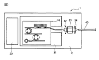
図1は、従来例の波長可変レーザ装置を示す図である。 FIG. 1 is a diagram showing a conventional tunable laser device.
波長可変レーザ装置101は、生成したレーザを光ファイバ140に向かって出力する光素子110と、コリメートレンズ132と、ビームスプリッタ135と、集光レンズ134と、エタロン136と、受光部118aを備える。
The wavelength
光素子110が生成した光の一部は、ビームスプリッタ135で分岐されて、エタロン136を介して、受光部118aにおいて受光される。また、ビームスプリッタ135を透過した光は、集光レンズ134により光ファイバ140に集光される。
Part of the light generated by the
また、波長可変レーザ装置101が生成したレーザの一部は、光ファイバ140とは反対側に出力されて、コリメートレンズ132を介して、受光部118bにおいて受光される。受光部118bで受光された光の強度は、光素子110におけるレーザの出力の制御に用いられる。
In addition, a part of the laser generated by the wavelength
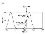
図2に示すように、エタロン136の光の透過率は、波長に対して周期的に変化する。従って、光素子110が生成した光の発振波長によって、エタロン136を透過する光の強度が変化する。受光部118aにより光の強度が検出されて、光素子110が発振しているレーザの発振波長が検出される。
As shown in FIG. 2, the light transmittance of the
通常、目標とする波長(グリッド波長)は、エタロン136の波長に対する透過率の変化率が大きい(スロープの傾きが大きい)波長の位置に設定される。
Normally, the target wavelength (grid wavelength) is set at a wavelength position where the transmittance change rate with respect to the wavelength of the
光素子110の発振波長が目標とする波長よりも長波長側にずれると、光のエタロン136の透過率が上昇して、受光部118aで検出される光の強度が増加するので、光素子110の発振波長を、短波長側に短くするように制御される。
When the oscillation wavelength of the
一方、光素子110の発振波長が目標とする波長よりも短波長側にずれると、光のエタロン136の透過率が下降して、受光部118aで検出される光の強度が減少するので、光素子110の発振波長は、長波長側に長くするように制御される。
On the other hand, when the oscillation wavelength of the
このようにして、波長可変レーザ装置101が発振するレーザの発振波長が検出されて、グリッド波長と一致した波長でレーザが出力されるように動的に制御される。
In this way, the oscillation wavelength of the laser oscillated by the wavelength
図1に示す例では、エタロンを用いた発振波長を検出するための光学素子を、光素子110の光路方向の横に並列して配置している。また、発振波長を検出するための光学素子は、光素子110の光路方向と直列する位置(受光部118b側の位置)に配置してもよい。
In the example shown in FIG. 1, an optical element for detecting an oscillation wavelength using an etalon is arranged in parallel along the optical path direction of the
図1に示すように、エタロンを用いて光素子の発振波長を検出することは、ビームスプリッタ又はエタロン等の光学素子を光路方向に並列又は直列して配置するので、波長可変レーザ装置の寸法を増加する要因となる。 As shown in FIG. 1, detecting the oscillation wavelength of an optical element using an etalon arranges optical elements such as a beam splitter or an etalon in parallel or in series in the optical path direction. It becomes an increase factor.
一方、近年、波長可変レーザ装置等の光モジュールの寸法(フォームファクタ)を低減することが求められている。そのため、波長可変レーザ装置においてもCFP2又はCFP4等に対応するべく装置の小型化が図られており、上述したように光学素子を光路に並列又は直列して配置することは困難になってきている。 On the other hand, in recent years, it has been required to reduce the size (form factor) of an optical module such as a wavelength tunable laser device. For this reason, in the wavelength tunable laser device, the size of the device is reduced so as to correspond to CFP2 or CFP4, and it has become difficult to arrange the optical elements in parallel or in series in the optical path as described above. .
また、シリコンプラットフォーム上に、入力光の波長に対して周期的な透過特性を有するリング共振器又は非対称マッハツェンダ型干渉フィルタ等の半導体素子を集積してエタロンと同様の機能を実現することも提案されている。しかし、これらの半導体素子は、エタロンを形成する石英等の誘電体材料を用いた光学素子と比べて屈折率の波長分散が大きい。そのため、エタロンと同様の周期的な光透過特性を有するリング共振器等を形成しても、光の透過特性のピークの間隔(Free Spectral Range:FSR)が不等間隔となる。従って、これらの半導体素子を用いると、等間隔なグリッド波長(実際は周波数グリッド)が得られないので、発振波長の制御が複雑になる。 It has also been proposed to integrate a semiconductor device such as a ring resonator or an asymmetric Mach-Zehnder interference filter having a periodic transmission characteristic with respect to the wavelength of the input light on a silicon platform to realize the same function as an etalon. ing. However, these semiconductor elements have a larger wavelength dispersion of the refractive index than an optical element using a dielectric material such as quartz forming an etalon. For this reason, even if a ring resonator or the like having a periodic light transmission characteristic similar to that of an etalon is formed, the peak interval (Free Spectral Range: FSR) of the light transmission characteristic becomes unequal. Therefore, using these semiconductor elements makes it difficult to control the oscillation wavelength because an equally spaced grid wavelength (actually a frequency grid) cannot be obtained.
本発明は、光素子を小型化することを課題とする。 An object of the present invention is to downsize an optical element.
また、本発明は、光生成装置を小型化することを課題とする。 Another object of the present invention is to reduce the size of the light generation device.
1つの態様では、光素子は、光導波路と、前記光導波路に沿って配置される複数の回折格子であって、前記回折格子それぞれは、前記光導波路を伝搬する光の一部を、前記光導波路の延びる向きと交差する方向に反射し、各前記回折格子が反射する光の反射光スペクトルの最大値の波長が異なっている複数の回折格子と、を備える。 In one aspect, the optical element is an optical waveguide and a plurality of diffraction gratings arranged along the optical waveguide, and each of the diffraction gratings transmits a part of light propagating through the optical waveguide to the optical waveguide. A plurality of diffraction gratings that are reflected in a direction intersecting with the extending direction of the waveguide and that have different maximum wavelengths of reflected light spectra of light reflected by the diffraction gratings.
また、1つの態様では、光生成装置は、光導波路と、前記光導波路に沿って配置される複数の回折格子であって、前記回折格子それぞれは、前記光導波路を伝搬する光の一部を、前記光導波路の延びる向きと交差する方向に反射し、各前記回折格子が反射する光の反射光スペクトルの最大値の波長が異なっている複数の回折格子と、を有する光素子と、生成した光を前記光導波路に伝搬させる光生成部と、前記光導波路内で発振する光の波長を選択する波長選択部と、前記光導波路内で、前記波長選択部により選択された波長の光を発振させる発振部と、を備える。 In one aspect, the light generation device includes an optical waveguide and a plurality of diffraction gratings arranged along the optical waveguide, wherein each of the diffraction gratings transmits a part of light propagating through the optical waveguide. An optical element having a plurality of diffraction gratings that are reflected in a direction intersecting with an extending direction of the optical waveguide and that have different maximum wavelengths of reflected light spectra of light reflected by the diffraction gratings. A light generation unit that propagates light to the optical waveguide, a wavelength selection unit that selects a wavelength of light that oscillates in the optical waveguide, and a light having a wavelength that is selected by the wavelength selection unit in the optical waveguide An oscillating unit to be provided.
1つの側面として、光素子を小型化することができる。 As one aspect, the optical element can be reduced in size.
また、1つの側面として、異なる波長の光を生成する光生成装置を小型化できる。 Further, as one aspect, a light generation device that generates light of different wavelengths can be downsized.
本発明の目的及び効果は、特に請求項において指摘される構成要素及び組み合わせを用いることによって認識され且つ得られるだろう。 The objects and advantages of the invention will be realized and obtained by means of the elements and combinations particularly pointed out in the appended claims.
前述の一般的な説明及び後述の詳細な説明の両方は、例示的及び説明的なものであり、特許請求の範囲に記載されている本発明を制限するものではない。 Both the foregoing general description and the following detailed description are exemplary and explanatory and are not restrictive of the invention as claimed.
以下、本明細書で開示する波長可変レーザ装置の好ましい第1実施形態を、図面を参照して説明する。但し、本発明の技術範囲はそれらの実施形態に限定されず、特許請求の範囲に記載された発明とその均等物に及ぶものである。 Hereinafter, a preferred first embodiment of a wavelength tunable laser device disclosed in this specification will be described with reference to the drawings. However, the technical scope of the present invention is not limited to these embodiments, but extends to the invention described in the claims and equivalents thereof.
図3は、本明細書に開示する第1実施形態の波長可変レーザ装置を示す図である。図4は、第1実施形態の波長可変レーザ装置の要部である光素子を示す図である。図5は、図4のX1−X1線拡大断面図である。図6は、図4のX2−X2線拡大断面図である。 FIG. 3 is a diagram illustrating the wavelength tunable laser device according to the first embodiment disclosed in this specification. FIG. 4 is a diagram illustrating an optical element that is a main part of the wavelength tunable laser device according to the first embodiment. FIG. 5 is an enlarged sectional view taken along line X1-X1 of FIG. 6 is an enlarged sectional view taken along line X2-X2 of FIG.
本実施形態の波長可変レーザ装置1(以下、単に装置1ともいう)は、発振するレーザの波長を変化させてレーザを生成する。そのため、装置1は、発振しているレーザの波長を検出して、目標とする波長と一致していない場合には、目標とする波長と一致するように発振波長の制御が行われる。
The wavelength
装置1は、所定の波長でレーザを発振して出力する光素子10と、光素子10の温度を制御する温度調整部31と、光素子10及び温度調整部31の動作を制御する制御部30を備える。
The
また、装置1は、光素子10から出力された光を平行光に変換するコリメートレンズ32と、平行光を光ファイバ40に集光する集光レンズ34と、戻り光が光素子10へ入射することを阻止するアイソレータ33を備える。集光レンズ34から出力された光は、光ファイバ40を伝搬して外部へ出力される。光素子10と、温度調整部31と、制御部30と、アイソレータ33等の光学素子は、基板2上に配置される。
The
図4に示すように、光素子10は、3つの光導波路12a〜12cと、2つのリング共振器13a、13bと、光生成部20と、ループミラー14等の光学素子を有する。3つの光導波路12a〜12cは、直線状に延びており、間隔をあけて並べて配置される。各光学素子は、光生成部20を除いて、シリコンプラットフォーム技術を用いて、一枚のシリコンの基板11a上に集積される。3つの光導波路12a〜12c及び2つのリング共振器13a、13bとして、例えばシリコン細線光導波路を用いることができる。
As illustrated in FIG. 4, the
リング共振器13aは、光導波路12aと光導波路12bとの間に配置される。光導波路12a及び光導波路12bは、リング共振器13aと光学的に結合する。また、リング共振器13bは、光導波路12bと光導波路12cとの間に配置される。光導波路12b及び光導波路12cは、リング共振器13bと光学的に結合する。
The
リング共振器13aは、リング共振器13aを透過する光の透過率が、波長と共に周期的に変化する。同様に、リング共振器13bも、リング共振器13bを透過する光の透過率が、波長と共に周期的に変化する。リング共振器13a及びリング共振器13bを透過する光の透過特性は、その曲率半径及び屈折率等に基づいて決定される。リング共振器13aの曲率半径は、リング共振器13bとは異なっていることが、バーニア効果を用いて、発振する波長を精度良く制御する観点から好ましい。例えば、リング共振器13aの曲率半径を700μmとし、リング共振器13bの曲率半径を650μmとすることができる。なお、ループミラー14の曲率半径は、300μmとすることができる。
In the
リング共振器13aの上には、リング共振器13aの温度を変化させて屈折率を変えることにより、光の透過特性を変化させるヒータ16aが配置される。同様に、リング共振器13bの上にも、リング共振器13bの温度を変化させて屈折率を変えることにより、光の透過特性を制御するヒータ16bが配置される。
A
また、光導波路12cにおける長手方向のループミラー14側の部分の上には、光導波路12cの温度を変化させて屈折率を変えることにより、伝搬する光の位相を制御するヒータ16cが配置される。
A
ヒータ16a〜16cは、アルミニウムあるいはチタン等の電流を流すことにより発熱する金属層を用いて形成され得る。ヒータ16a〜16cの動作は、制御部30により制御される。
The
図6に示すように、光素子10では、シリコンの基板11a上にクラッド層11bが配置され、3つの光導波路12a〜12c及び2つのリング共振器13a、13bは、クラッド層11b内に埋め込まれている。クラッド層11b上には、上クラッド層11cが配置される。クラッド層11b及び上クラッド層11cは、例えば、酸化シリコンを用いて形成され得る。
As shown in FIG. 6, in the
3つの光導波路12a〜12c及び2つのリング共振器13a、13bの厚さは、例えば250nmとすることができ、幅は、例えば500nmとすることができる。光導波路12aとリング共振器13aとの距離は、例えば180nmとすることができる。
The thickness of the three
光生成部20は、光を生成し、生成した光を光導波路12aに伝搬させる。光生成部20は、電流が注入されて光子を生成する利得部を有する光導波路21を有する。光生成部20としては、例えば、化合物半導体を有する半導体光増幅素子を用いることができる。利得部としては、量子井戸活性層、量子ドット活性層、バルク型の活性層等を用いることができる。光導波路21は、光生成部20の第2端面20b側において、光導波路12aと光学的に結合する。光導波路21は、第2端面20bに対して、その法線から所定の角度(例えば7度)だけ傾斜して延びている。光導波路12aも、第2端面20bに対して、その法線から所定の角度(例えば15度)だけ傾斜して延びている。
The
光素子10を伝搬する光の経路は、光生成部20の光導波路21と、光導波路12a〜12cと、リング共振器13a、13bにより形成される。この光の経路を伝搬する光は、光生成部20の第1端面20aと、光導波路12cの一方の端部に光学的に結合されるループミラー14との間で反射するようになされている。即ち、装置1は、発振部(共振部)として、光生成部20の第1端面20a及びループミラー14を備える。光生成部20の第1端面20aは、光導波路21を第1端面20aに向かって伝搬して来た光の一部を第2端面20b側に向かって反射する。また、光生成部20の第1端面20aは、光導波路21を第1端面20aに向かって伝搬して来た光の他の部分を外部へ透過して、レーザとして出力する。光生成部20の第1端面20aは、例えば、劈開面を用いることができる。ループミラー14は、光導波路12cをループミラー14に向かって伝搬して来た光を反対側に向かって反射する。
The path of light propagating through the
光導波路12a〜12c及び光導波路21を含む光路長は、発振するレーザに対して求められるスペクトル幅に応じて、適宜決定され得る。一般に、光路長を長くする程、狭いスペクトル幅を得ることができる。
The optical path length including the
次に、光素子10において、発振波長を検出する仕組みを以下に説明する。
Next, a mechanism for detecting the oscillation wavelength in the
光素子10は、光導波路12aに沿って配置される複数の回折格子DBR1〜DBR11を有する。本実施形態では、光素子10は、11個の回折格子DBR1〜DBR11を有する。それぞれの回折格子は、光導波路12aを伝搬する光の一部を、光導波路12aの延びる向きと交差する方向に反射する。本実施形態では、回折格子DBR1〜DBR11それぞれは、光導波路12aを伝搬する光の一部を、光導波路12aの延びる向きと直交する同じ方向(図4の上方)に向かって反射する。
The
図5に示すように、複数の回折格子DBR1〜DBR11は、光導波路12aに沿って直列に並べて配置される。複数の回折格子DBR1〜DBR11は、クラッド層11bが上方から加工されて形成され得る。光導波路12aを伝搬する光に対する、回折格子の反射率及び反射光ピーク幅(帯域幅)は、回折格子の結合定数に基づいて決定され得る。回折格子の結合定数は、溝の深さ及び光導波路12aとの距離等に基づいて決定され得る。複数の回折格子DBR1〜DBR11が形成されるクラッド層11b上には、回折格子の溝を埋め込むように、上クラッド層11cが配置される。複数の回折格子DBR1〜DBR11は、シリコンプラットフォーム技術を用いて、他の光学素子と共にシリコンの基板上に配置することができる。
As shown in FIG. 5, the plurality of diffraction gratings DBR1 to DBR11 are arranged in series along the
上クラッド層11c上には、ヒータ15が配置される。ヒータ15は、各回折格子DBR1〜DBR11の上方に配置される。各回折格子DBR1〜DBR11の反射光のピーク波長は、回折格子の溝の周期に基づいて決定されるが、製造工程等の影響により回折格子の寸法に誤差が生じ得る。この回折格子の寸法の誤差に基づく反射光のピーク波長のずれを、ヒータ15による加熱を用いて、各回折格子を含む部分の屈折率を変化させることにより調整する。ヒータ15の動作は、制御部30により制御される。
A
図7に示すように、各回折格子DBR1〜DBR11は、光導波路12aの延びる向きと交差する方向に延びる、周期的に形成された複数の溝を有する。
As shown in FIG. 7, each of the diffraction gratings DBR1 to DBR11 has a plurality of periodically formed grooves extending in a direction intersecting with the extending direction of the
具体的には、各回折格子DBR1〜DBR11には、光導波路12aの光が伝搬する光軸方向に対して45度傾斜した向きを有する複数の溝が所定の周期で形成される。各回折格子DBR1〜DBR11は、光導波路12aを伝搬する光の一部を、光軸方向と直交する向きに反射して、光導波路17に導波する。光導波路17を伝搬する光は、受光部18により受光される。受光部18は、受光した光の強度を電気信号に変換して制御部30に出力する。各回折格子DBR1〜DBR11と対応させて配置される11個の受光部18は、受光部のアレイ18Aを形成する。受光部18は、例えば、Ge又はSiGe等を用いて形成される。
Specifically, each of the diffraction gratings DBR1 to DBR11 is formed with a plurality of grooves having a direction inclined by 45 degrees with respect to the optical axis direction in which the light of the
光導波路17及び受光部18の各組は、各回折格子DBR1〜DBR11に対して配置される。回折格子それぞれで反射された反射光は、各回折格子に接続された光導波路17を伝搬して、各受光部18において受光される。隣接する回折格子が反射した反射光は、隣接して配置される異なる受光部18により受光される。
Each set of the
回折格子DBR1〜DBR11の長さは、例えば50μmとすることができる。隣接する回折格子同士の間の距離は、例えば5μmとすることができる。回折格子DBR1〜DBR11と、受光部18とを接続する光導波路17の幅は、例えば回折格子の長さと同じ50μmとすることができる。
The length of the diffraction gratings DBR1 to DBR11 can be set to, for example, 50 μm. The distance between adjacent diffraction gratings can be set to 5 μm, for example. The width of the
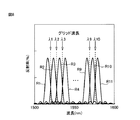
図8は、複数の回折格子の反射光スペクトルを示す図である。 FIG. 8 is a diagram showing reflected light spectra of a plurality of diffraction gratings.
各回折格子DBR1〜DBR11は、異なる周期の溝を有しており、反射する光の反射光スペクトルの最大値の波長が異なっている。即ち、一の回折格子の溝の周期及び反射光スペクトルの最大値の波長は、他の回折格子とは異なっている。 Each of the diffraction gratings DBR1 to DBR11 has grooves with different periods, and the maximum wavelength of the reflected light spectrum of the reflected light is different. That is, the groove period of one diffraction grating and the maximum wavelength of the reflected light spectrum are different from those of other diffraction gratings.
反射光スペクトルの最大値は、回折格子の結合定数に基づいて決定され得る。回折格子の結合定数が増加するのと共に、反射光スペクトルの最大値も増大する。反射光スペクトルの最大値が増大すると、受光部18における受光量が増加するので、発振波長の検出精度が向上し得る。
The maximum value of the reflected light spectrum can be determined based on the coupling constant of the diffraction grating. As the coupling constant of the diffraction grating increases, the maximum value of the reflected light spectrum also increases. When the maximum value of the reflected light spectrum increases, the amount of light received by the
一方、反射光スペクトルの最大値が増大するのと共に、光導波路12aを伝搬する光量が減少するので、光素子10から出力されるレーザの強度が低減する。回折格子の結合定数を大きくすると、光導波路を伝搬する光の量を減少し、結合定数を小さくすると、反射する反射光量を低減するので、発振波長の検出精度に影響を与え得る。
On the other hand, the maximum value of the reflected light spectrum increases and the amount of light propagating through the
従って、回折格子の結合定数は、上述した観点を考慮して適宜決定され得る。例えば、回折格子の溝における山谷の比を1:1とし、結合係数は150cm−1として、反射光スペクトルの最大値を40%としてもよい。 Therefore, the coupling constant of the diffraction grating can be appropriately determined in consideration of the above-described viewpoint. For example, the ratio of peaks and valleys in the grooves of the diffraction grating may be 1: 1, the coupling coefficient may be 150 cm −1 , and the maximum value of the reflected light spectrum may be 40%.
一の回折格子の反射光スペクトルの包絡線R1〜R11は、該反射光スペクトルの最大値の1/10以上、好ましくは3/10以上の大きさのスペクトル成分を有する波長の位置で、他の回折格子の反射光スペクトルの包絡線と交差している。 Envelopes R1 to R11 of the reflected light spectrum of one diffraction grating are positions of wavelengths having spectral components having a magnitude of 1/10 or more, preferably 3/10 or more of the maximum value of the reflected light spectrum. It intersects with the envelope of the reflected light spectrum of the diffraction grating.
具体的には、一の回折格子DBR1の反射光スペクトルの包絡線R1は、該反射光スペクトルの最大値の1/10以上、好ましくは3/10以上の大きさのスペクトル成分を有する波長の位置で、隣接する他の回折格子DBR2の反射光スペクトルの包絡線R2と交差している。この説明は、他の隣接する回折格子同士に対しても適用される。本実施形態では、隣接する回折格子の反射光スペクトルの包絡線R1〜R11同士が交差する位置は、反射光スペクトルの最大値の1/2の大きさのスペクトル成分を有する波長の位置に設定される。 Specifically, the envelope R1 of the reflected light spectrum of one diffraction grating DBR1 is a wavelength position having a spectral component having a magnitude of 1/10 or more, preferably 3/10 or more of the maximum value of the reflected light spectrum. And intersects with the envelope R2 of the reflected light spectrum of another adjacent diffraction grating DBR2. This description also applies to other adjacent diffraction gratings. In the present embodiment, the position where the envelopes R1 to R11 of the reflected light spectrum of adjacent diffraction gratings intersect is set to the position of the wavelength having a spectral component that is 1/2 the maximum value of the reflected light spectrum. The
また、一の回折格子の反射光スペクトルの包絡線R1〜R11が、一の回折格子に隣接する他の回折格子の反射光スペクトルの包絡線と交差する波長の位置は等間隔である。本実施形態では、隣接する回折格子の反射光スペクトルの包絡線R1〜R11同士が、反射光スペクトルの最大値の1/10以上のスペクトル成分を有する波長において交差する位置は、4.5nm(周波数50GHz)の間隔で配置される。
Further, the positions of the wavelengths at which the envelopes R1 to R11 of the reflected light spectrum of one diffraction grating intersect with the envelopes of the reflected light spectrum of other diffraction gratings adjacent to the one diffraction grating are equally spaced. In the present embodiment, the position where the envelopes R1 to R11 of the reflected light spectrum of adjacent diffraction gratings intersect at a wavelength having a spectral component of 1/10 or more of the maximum value of the reflected light spectrum is 4.5 nm (
なお、一の回折格子DBR1の反射光スペクトルの包絡線と、該反射光スペクトルの最大値の1/10以上の大きさのスペクトル成分を有する波長の位置で交差する反射光スペクトルの包絡線を有する回折格子は、隣接する回折格子でなくてもよい。また、一の回折格子の反射光スペクトルの包絡線R1〜R11が、一の回折格子に隣接する他の回折格子の反射光スペクトルの包絡線と交差する波長の位置は、不等間隔であってもよい。 In addition, the envelope of the reflected light spectrum of one diffraction grating DBR1 and the envelope of the reflected light spectrum intersect at a wavelength position having a spectral component having a magnitude of 1/10 or more of the maximum value of the reflected light spectrum. The diffraction grating may not be an adjacent diffraction grating. The positions of the wavelengths at which the envelopes R1 to R11 of the reflected light spectrum of one diffraction grating intersect the envelopes of the reflected light spectrum of other diffraction gratings adjacent to the one diffraction grating are unequal intervals. Also good.
図8に示すように、これらの隣接する回折格子の反射光スペクトルの包絡線R1〜R11同士が交差する波長の位置は、装置1が発振するレーザの目標とする波長(グリッド波長)λ1〜λ10と一致するように決定され得る。
As shown in FIG. 8, the positions of the wavelengths where the envelopes R1 to R11 of the reflected light spectra of these adjacent diffraction gratings intersect with each other are the target wavelengths (grid wavelengths) λ1 to λ10 of the laser oscillated by the
次に、本実施形態の11個の回折格子DBR1〜DBR11の寸法の例について、以下に説明する。 Next, examples of dimensions of the eleven diffraction gratings DBR1 to DBR11 of the present embodiment will be described below.
回折格子DBR1〜DBR11は、回折格子の周期が、410.060nmから420.923nmの範囲にある。これらの回折格子DBR1〜DBR11により反射される反射光スペクトルの中心波長は、4.5nmの間隔で、1528.084nmから1568.563nmの範囲にある。 The diffraction gratings DBR1 to DBR11 have a diffraction grating period in the range of 410.060 nm to 420.923 nm. The center wavelength of the reflected light spectrum reflected by these diffraction gratings DBR1 to DBR11 is in the range of 1528.084 nm to 1568.563 nm at an interval of 4.5 nm.
回折格子DBR1及び隣接する回折格子DBR2の反射光スペクトルの包絡線R1,R2の交点の波長の位置は、1530.334nm(周波数195.9THz)であり、グリッド波長λ1となる。同様にして、回折格子DBR2及び隣接する回折格子DBR3の反射光スペクトルの包絡線R2,R3の交点の波長の位置は、グリッド波長λ2となる。以下同様にして、回折格子DBR10及び隣接する回折格子DBR11の反射光スペクトルの包絡線R10,R11の交点の波長の位置は、グリッド波長λ10となる。 The position of the wavelength of the intersection of the envelopes R1 and R2 of the reflected light spectrum of the diffraction grating DBR1 and the adjacent diffraction grating DBR2 is 1530.334 nm (frequency 195.9 THz), which is the grid wavelength λ1. Similarly, the position of the wavelength at the intersection of the envelopes R2 and R3 of the reflected light spectrum of the diffraction grating DBR2 and the adjacent diffraction grating DBR3 is the grid wavelength λ2. Similarly, the position of the wavelength of the intersection of the envelopes R10 and R11 of the reflected light spectrum of the diffraction grating DBR10 and the adjacent diffraction grating DBR11 is the grid wavelength λ10.
例えば、光素子10が、グリッド波長λ1で発振している時には、光導波路12aを伝搬する光の波長は、回折格子DBR1及び隣接する回折格子DBR2の反射光スペクトルの包絡線R1,R2の交点の波長の付近に位置する。そのため、光導波路12aを伝搬する光の一部は、隣接する2つの回折格子DBR1、DBR2により反射されて、反射した光それぞれは、光導波路17を介して隣接する2つの受光部18により受光される。
For example, when the
この場合、グリッド波長λ1の波長は、回折格子DBR3〜DBR11の反射光スペクトルの包絡線R3〜R11の波長とは実質的に重ならないので(図8参照)、回折格子DBR3〜DBR11は、光導波路12aを伝搬する光を反射しない。従って、回折格子DBR3〜DBR11は、光導波路12aを伝搬するグリッド波長λ1付近の光に対して、回折格子DBR3〜DBR11は実質的に透明となる。
In this case, since the wavelength of the grid wavelength λ1 does not substantially overlap with the wavelengths of the envelopes R3 to R11 of the reflected light spectrum of the diffraction gratings DBR3 to DBR11 (see FIG. 8), the diffraction gratings DBR3 to DBR11 are optical waveguides. The light propagating through 12a is not reflected. Accordingly, the diffraction gratings DBR3 to DBR11 are substantially transparent with respect to light in the vicinity of the grid wavelength λ1 propagating through the
本明細書において、光導波路12aを伝搬する光の波長が、回折格子の反射光スペクトルの包絡線の波長とは実質的に重ならないことは、光導波路12aを伝搬する光の波長が、反射光スペクトルの最大値の1/10以上の波長の領域で重ならないことを意味する。
In this specification, the fact that the wavelength of light propagating through the
また、一の回折格子DBR1、DBR2の反射光スペクトルの包絡線R1、R2は、該反射光スペクトルの最大値の1/10以上、好ましくは1/30の大きさのスペクトル成分を有する波長の領域では、一の回折格子DBR1、DBR2とは隣接しない他の回折格子DBR3〜DBR11の反射光スペクトルの包絡線とは交差しない。上述した説明は、他の隣接する回折格子にも適宜適用される。 The envelopes R1 and R2 of the reflected light spectrum of one diffraction grating DBR1 and DBR2 are wavelength regions having a spectral component having a magnitude of 1/10 or more, preferably 1/30 of the maximum value of the reflected light spectrum. Then, it does not intersect with the envelope of the reflected light spectrum of the other diffraction gratings DBR3 to DBR11 that are not adjacent to one diffraction grating DBR1 and DBR2. The above description is also applied as appropriate to other adjacent diffraction gratings.
また、グリッド波長λ1の光を発振している場合、光は、光生成部20の第1端面20aとループミラー14との間で反射しているが、回折格子DBR1、DBR2により反射される光は、光導波路17に向かって反射される。そのため、回折格子DBR1、DBR2により反射される光が、光導波路12aを含む光経路の発振に与える影響は実質的にはないと考えられる。
When the light having the grid wavelength λ1 is oscillated, the light is reflected between the
各回折格子DBR1〜DBR11は、反射光スペクトルの包絡線R1〜R11の交差する位置に対応するグリッド波長λ1〜λ10の光を受光部18に向かって反射する機能を有するが、グリッド波長λ1〜λ10の光の発振には実質的には影響を与えない。
Each of the diffraction gratings DBR1 to DBR11 has a function of reflecting the light of the grid wavelengths λ1 to λ10 corresponding to the positions where the envelopes R1 to R11 of the reflected light spectrum intersect toward the
次に、グリッド波長λ1〜λ11の光を発振するための制御について、以下に説明する。 Next, control for oscillating light of grid wavelengths λ1 to λ11 will be described below.
まず、グリッド波長λ1を目標として光を発振する場合を考える。 First, consider a case where light is oscillated with the grid wavelength λ1 as a target.
制御部30は、グリッド波長λ1の光を発振するために、リング共振器13a、13b及び光導波路12cの屈折率を、予め設定されている値となるように、各ヒータ16a〜16cを制御する。その結果、光導波路12aには、グリッド波長λ1に近い波長λrを有する光が生成される。
The
波長λrは、回折格子DBR1、DBR2の反射光スペクトルの波長領域とで重なるので、回折格子DBR1及び回折格子DBR2は、光導波路12aを伝搬する光の一部を反射する。反射光は、光導波路17を介して、隣接する2つの受光部18で受光される。各受光部18は、受光強度を電気信号に変換して制御部30へ出力する。
Since the wavelength λr overlaps with the wavelength region of the reflected light spectrum of the diffraction gratings DBR1 and DBR2, the diffraction grating DBR1 and the diffraction grating DBR2 reflect a part of the light propagating through the
図9(A)に示すように、光導波路12aを伝搬する光の波長λrが、グリッド波長λ1と一致する場合には、回折格子DBR1により反射される反射光の強度S1と、回折格子DBR2により反射される反射光の強度S2とが等しくなる。波長λrが、グリッド波長λ1と一致することには、受光部18により受光される光の強度に対して許容される誤差を設けてもよい。
As shown in FIG. 9A, when the wavelength λr of the light propagating through the
次に、図9(B)に示すように、光導波路12aを伝搬する光の波長λrが、グリッド波長λ1よりも大きい場合には、回折格子DBR1により反射される反射光の強度S1は、回折格子DBR2により反射される反射光の強度S2よりも小さくなる。
Next, as shown in FIG. 9B, when the wavelength λr of the light propagating through the
この場合には、制御部30は、ヒータ16a〜16cを制御し、リング共振器13a、13b又は光導波路12cの屈折率を調整して、回折格子DBR1により反射される反射光の強度S1と、回折格子DBR2により反射される反射光の強度S2とを一致させる。
In this case, the
また、図9(C)に示すように、光導波路12aを伝搬する光の波長λrが、グリッド波長λ1よりも小さい場合には、回折格子DBR1により反射される反射光の強度S1は、回折格子DBR2により反射される反射光の強度S2よりも大きくなる。
As shown in FIG. 9C, when the wavelength λr of the light propagating through the
この場合には、制御部30は、ヒータ16a〜16cを制御し、リング共振器13a、13b又は光導波路12cの屈折率を調整して、回折格子DBR1により反射される反射光の強度S1と、回折格子DBR2により反射される反射光の強度S2とを一致させる。
In this case, the
このようにして、光導波路12aを伝搬する光の波長λrを検出して、グリッド波長λ1〜λ10と一致するように波長λrが制御される。また、波長λrを制御した結果、発振される光の強度が変化した場合には、光生成部20に注入する電流も制御され得る。
In this way, the wavelength λr of the light propagating through the
光導波路12aを伝搬する光の波長λrを検出する感度を高める観点からは、反射光スペクトルの包絡線の傾きの大きい位置で、隣接する反射光スペクトルの包絡線を交差させることが好ましい。
From the viewpoint of increasing the sensitivity for detecting the wavelength λr of light propagating through the
同様にして、他のグリッド波長λ2〜λ10において発振する光の波長が制御される。 Similarly, the wavelengths of light oscillated at other grid wavelengths λ2 to λ10 are controlled.
上述した本実施形態の装置1によれば、異なる波長で発振する光の波長を、複数の回折格子を用いて検出する。複数の回折格子は、シリコンプラットフォーム技術を用いて、他の光学素子と共にシリコンの基板上に配置することができるので、光素子を小型化することができる。そのため、小型化した波長可変レーザ装置を実現できる。
According to the
また、上述した本実施形態では、一の回折格子の反射光スペクトルの包絡線R1〜R11が、一の回折格子に隣接する他の回折格子の反射光スペクトルの包絡線と交差する波長の位置は等間隔であった。装置1では、隣接する回折格子同士の反射光スペクトルの包絡線が交差する波長の位置は、回折格子の溝の周期の設計により変更可能であり、不等間隔にすることもできる。このようにグリッド波長が不等間隔であっても、2つの受光部により受光される光強度を一致させるようにして、発振波長を容易に制御できる。
In the above-described embodiment, the position of the wavelength where the envelopes R1 to R11 of the reflected light spectrum of one diffraction grating intersect the envelope of the reflected light spectrum of another diffraction grating adjacent to the one diffraction grating is It was equally spaced. In the
次に、上述した第1実施形態の波長可変レーザ装置の変形例1及び変形例2を、図面を参照しながら、以下に説明する。
Next,
図10は、第1実施形態の変形例1の光素子を示す図である。
FIG. 10 is a diagram illustrating an optical element according to
本変型例の光素子10では、各回折格子DBR1〜DBR11に対して、光導波路12aの両側の位置に、光導波路17及び受光部18が配置されて、光導波路12aの両側に受光部のアレイ18A及び受光部のアレイ18Bが配置される。
In the
上述した第1実施形態では、図7に示すように、各回折格子DBR1〜DBR11は、光導波路12aを左側から右側に向かって伝搬する光を上方に反射して、反射光が受光部18で受光される。一方、光導波路12aを右側から左側に向かって伝搬する光は、各回折格子DBR1〜DBR11において反射されるが、光導波路及び受光部が配置されていないので、反射光が検出されることはない。
In the first embodiment described above, as shown in FIG. 7, each of the diffraction gratings DBR <b> 1 to DBR <b> 11 reflects light propagating through the
そこで、本変型例の光素子10では、光導波路12aを右側から左側に向かって伝搬する光も下方に反射して、受光して検出することにより、発振している波長の検出精度を向上できるようになされている。
Therefore, in the
図11は、第1実施形態の変形例2の光素子を示す図である。図12は、図11の要部を示す図である。
FIG. 11 is a diagram illustrating an optical element according to
本変型例の光素子10では、回折格子DBR1〜DBR11と受光部18との間に光導波路が配置されない点が、上述した変形例1とは異なっている。
The
図12に示すように、各回折格子DBR1〜DBR11が配置される光導波路12aの領域に対して間隔をあけて受光部18が両側に配置される。受光部18は、クラッド層11b内に埋め込まれている。光導波路12aと受光部18との間の距離を、光導波路12aを伝搬する光のエンベロープが十分に低減した距離に設定することが、光導波路12aを伝搬する光の強度を低減し過ぎない観点から好ましい。
As shown in FIG. 12, the
本変型例によれば、回折格子DBR1〜DBR11と受光部18との間に光導波路が配置されないことにより、光素子10の寸法を低減すると共に、受光部18に受光される反射光の強度を高めることができる。
According to this modified example, since the optical waveguide is not disposed between the diffraction gratings DBR1 to DBR11 and the
次に、上述した光生成装置の第2実施形態を、図13〜図18を参照しながら以下に説明する。第2実施形態について特に説明しない点については、上述の第1実施形態に関して詳述した説明が適宜適用される。また、同一の構成要素には同一の符号を付してある。 Next, a second embodiment of the light generation apparatus described above will be described below with reference to FIGS. For points that are not particularly described in the second embodiment, the description in detail regarding the first embodiment is applied as appropriate. Moreover, the same code | symbol is attached | subjected to the same component.
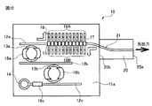
図13は、本明細書に開示する第2実施形態の波長可変レーザ装置を示す図である。図14は、第2実施形態の波長可変レーザ装置の要部である光素子を示す図である。図15は、図14のY1−Y1線拡大断面図である。図16は、図14のY2−Y2線拡大断面図である。 FIG. 13 is a diagram illustrating a wavelength tunable laser device according to a second embodiment disclosed in this specification. FIG. 14 is a diagram illustrating an optical element that is a main part of the wavelength tunable laser device according to the second embodiment. FIG. 15 is an enlarged sectional view taken along line Y1-Y1 of FIG. 16 is an enlarged sectional view taken along line Y2-Y2 of FIG.
本実施形態の光素子10は、複数の回折格子の配置と、回折格子の反射光を受光部に伝搬する光導波路と、受光部の構成が、上述した第1実施形態とは異なっている。
The
図15及び図17に示すように、光素子10は、光導波路12aに沿って直列に並べて配置される所定数の回折格子DBR1〜DBR4を有する第1グループG1を有する。また、光素子10は、光導波路12aに沿って並べて配置され、第1グループG1と同じ所定数の回折格子DBR5〜DBR8を有する第2グループG2を有する。第1グループG1と第2グループG2は、光素子12a沿って直列に配置される。本実施形態では、第1グループG1及び第2グループG2は、4つの回折格子を有する。
As shown in FIGS. 15 and 17, the
図17に示すように、第1グループG1の回折格子DBR1〜DBR4及び第2グループG1の回折格子DBR5〜DBR8は、光導波路12aの延びる向きと交差する方向に延びる、周期的に形成された複数の溝を有する。各グループG1,G2において、各回折格子は、間隔をあけずに配置される。
As shown in FIG. 17, the diffraction gratings DBR1 to DBR4 of the first group G1 and the diffraction gratings DBR5 to DBR8 of the second group G1 extend in a direction intersecting with the extending direction of the
各回折格子DBR1〜DBR8は、異なる周期の溝を有しており、反射する光の反射光スペクトルの最大値の波長が異なっている。即ち、一の回折格子の溝の周期及び反射光スペクトルの最大値の波長は、他の回折格子の溝の周期とは異なっている。 Each of the diffraction gratings DBR1 to DBR8 has grooves with different periods, and the maximum wavelength of the reflected light spectrum of the reflected light is different. That is, the groove period of one diffraction grating and the maximum wavelength of the reflected light spectrum are different from the groove period of the other diffraction grating.
図14及び図15に示すように、第1グループG1の回折格子DBR1〜DBR4の上方には、ヒータ15aが配置される。同様に、第2グループG2の回折格子DBR5〜DBR8の上方には、ヒータ15bが配置される。回折格子の寸法の誤差に基づく反射光のピーク波長のずれを、ヒータ15a、15bによる加熱を用いて、各グループの回折格子の部分の屈折率を変化させることにより調整する。ヒータ15a、15bの動作は、制御部30により制御される。
As shown in FIGS. 14 and 15, a
第1グループG1の回折格子DBR1〜DBR4それぞれは、光導波路12aを伝搬する光の一部を、光導波路12aの延びる向きと直交又は交差する向きに反射して、光導波路19aに導波する。光導波路19aを伝搬する光は、受光部18aにより受光される。受光部18aは、受光した反射光の強度を電気信号に変換して制御部30に出力する。
Each of the diffraction gratings DBR1 to DBR4 of the first group G1 reflects a part of light propagating through the
同様に、第2グループG2の各回折格子DBR5〜DBR8は、光導波路12aを伝搬する光の一部を、光軸方向と直交又は交差する向きに反射して、光導波路19bに導波する。光導波路19bを伝搬する光は、受光部18bにより受光される。受光部18bは、受光した反射光の強度を電気信号に変換して制御部30に出力する。
Similarly, each of the diffraction gratings DBR5 to DBR8 of the second group G2 reflects a part of the light propagating through the
光導波路19aは、第1グループG1の回折格子DBR1〜DBR4と接続する部分の幅は広く、受光部18aと接続する部分の幅は狭くなっており、全体としてテーパ形状を有する。光導波路19bも、光導波路19aと同様の形状を有する。
In the
各グループG1,G2の回折格子それぞれの長さは、例えば80μmとすることができる。第1グループG1と第2グループG2との間の距離は、例えば5μmとすることができる。 The length of each diffraction grating of each group G1, G2 can be set to 80 μm, for example. The distance between the first group G1 and the second group G2 can be set to 5 μm, for example.
例えば、回折格子DBR1〜DBR8の溝における山谷の比を1:1とし、結合係数は180cm−1として、反射光スペクトルの最大値を80%としてもよい。 For example, the ratio of peaks and valleys in the grooves of the diffraction gratings DBR1 to DBR8 may be 1: 1, the coupling coefficient may be 180 cm −1 , and the maximum value of the reflected light spectrum may be 80%.
図18は、第1グループ及び第2グループの回折格子の反射光スペクトルを示す図である。 FIG. 18 is a diagram illustrating reflected light spectra of the diffraction gratings of the first group and the second group.
第1グループG1の回折格子DBR1は、第2グループG2の回折格子DBR5と対になっている。同様に、第1グループG1の回折格子DBR2は第2グループG2の回折格子DBR6と、第1グループG1の回折格子DBR3は第2グループG2の回折格子DBR7と、第1グループG1の回折格子DBR4は第2グループG2の回折格子DBR8と、対になっている。 The diffraction grating DBR1 of the first group G1 is paired with the diffraction grating DBR5 of the second group G2. Similarly, the diffraction grating DBR2 of the first group G1 is the diffraction grating DBR6 of the second group G2, the diffraction grating DBR3 of the first group G1 is the diffraction grating DBR7 of the second group G2, and the diffraction grating DBR4 of the first group G1 is It is paired with the diffraction grating DBR8 of the second group G2.
第1グループG1の回折格子DBR1の反射光スペクトルの包絡線R1は、該反射光スペクトルの最大値の1/10以上の大きさのスペクトル成分を有する波長の位置で、対となる第2グループG2の回折格子DBR5の反射光スペクトルの包絡線R2と交差している。他の対となる回折格子の反射光スペクトルの包絡線同士も同様の関係を有する。 The envelope R1 of the reflected light spectrum of the diffraction grating DBR1 of the first group G1 is a position of a wavelength having a spectral component having a magnitude of 1/10 or more of the maximum value of the reflected light spectrum. This crosses the envelope R2 of the reflected light spectrum of the diffraction grating DBR5. The envelopes of the reflected light spectra of other pairs of diffraction gratings have the same relationship.
具体的には、第1グループG1の回折格子DBR1の反射光スペクトルの包絡線R1は、該反射光スペクトルの最大値の1/10以上、好ましくは3/10以上の大きさのスペクトル成分を有する波長の位置で、対となる第2グループG2の回折格子DBR5の反射光スペクトルの包絡線R5と交差している。この説明は、他の対となる回折格子の反射光スペクトルの包絡線に対しても適用される。本実施形態では、対となる回折格子の反射光スペクトルの包絡線同士が交差する位置は、反射光スペクトルの最大値の1/2の大きさのスペクトル成分を有する波長の位置に設定される。 Specifically, the envelope R1 of the reflected light spectrum of the diffraction grating DBR1 of the first group G1 has a spectral component having a magnitude of 1/10 or more, preferably 3/10 or more of the maximum value of the reflected light spectrum. At the position of the wavelength, it intersects with the envelope R5 of the reflected light spectrum of the diffraction grating DBR5 of the second group G2 as a pair. This explanation also applies to the envelope of the reflected light spectrum of another pair of diffraction gratings. In the present embodiment, the position where the envelopes of the reflected light spectrum of the diffraction gratings that are paired with each other is set to the position of the wavelength having a spectral component that is 1/2 the maximum value of the reflected light spectrum.
第1グループG1の一の回折格子DBR1〜DBR4の反射光スペクトルの包絡線R1〜R4が、対となる第2グループG2の回折格子DBR5〜DBR8の反射光スペクトルの包絡線R5〜R8と交差する波長の位置は等間隔である。本実施形態では、対となる反射光スペクトルの包絡線が交差する波長の間隔は、約20nmである。 The envelopes R1 to R4 of the reflected light spectra of the first diffraction gratings DBR1 to DBR4 of the first group G1 intersect the envelopes R5 to R8 of the reflected light spectra of the diffraction gratings DBR5 to DBR8 of the second group G2. The positions of the wavelengths are equally spaced. In the present embodiment, the interval between the wavelengths at which the envelopes of the reflected light spectrum forming a pair intersect is about 20 nm.
第1グループG1の回折格子DBR1の反射光スペクトルの包絡線R1は、該反射光スペクトルの最大値の1/10以上、好ましくは1/30以上の大きさのスペクトル成分を有する波長の領域では、対となる第2グループG2の回折格子DBR5以外の第1グループG1及び第2グループG2の他の回折格子DBR2〜DBR4、DBR6〜DBR8の反射光スペクトルの包絡線R2〜R4、R6〜R8とは交差しない。この説明は、他の回折格子に対しても適用される。 The envelope R1 of the reflected light spectrum of the diffraction grating DBR1 of the first group G1 is 1/10 or more, preferably 1/30 or more of the maximum value of the reflected light spectrum. What are the envelopes R2 to R4 and R6 to R8 of the reflected light spectra of the other diffraction gratings DBR2 to DBR4 and DBR6 to DBR8 of the first group G1 and the second group G2 other than the diffraction grating DBR5 of the second group G2 to be paired? Do not cross. This explanation also applies to other diffraction gratings.
図18に示すように、対となる第1グループG1及び第2グループG2の回折格子の反射光スペクトルの包絡線同士が交差する波長の位置は、装置1が発振するレーザの目標とする波長(グリッド波長)λ1〜λ4と一致するように決定され得る。 As shown in FIG. 18, the position of the wavelength where the envelopes of the reflected light spectra of the diffraction gratings of the first group G1 and the second group G2 that form a pair intersect each other is the target wavelength of the laser oscillated by the apparatus 1 ( (Grid wavelength) can be determined to coincide with λ1 to λ4.
次に、本実施形態の第1グループG1の回折格子DBR1〜DBR4及び第2グループG2の回折格子DBR5〜DBR8の寸法の例について、以下に説明する。 Next, examples of dimensions of the diffraction gratings DBR1 to DBR4 of the first group G1 and the diffraction gratings DBR5 to DBR8 of the second group G2 according to this embodiment will be described below.
第1グループG1の回折格子DBR1〜DBR4は、回折格子の周期が、410.06nmから431.33nmの範囲にある。回折格子DBR1により反射される反射光スペクトルの中心波長は、1528.084nmであり、回折格子DBR2〜DBR4により反射される反射光スペクトルの中心波長は、約20nmずつ増加する。 The diffraction gratings DBR1 to DBR4 of the first group G1 have a diffraction grating period in the range of 410.06 nm to 431.33 nm. The center wavelength of the reflected light spectrum reflected by the diffraction grating DBR1 is 1528.084 nm, and the center wavelength of the reflected light spectrum reflected by the diffraction gratings DBR2 to DBR4 increases by about 20 nm.
第2グループG2の回折格子DBR5〜DBR8は、回折格子の周期が、411.83nmから433.10nmの範囲にある。第2グループG2の回折格子DBR5〜DBR8それぞれにより反射される反射光スペクトルの中心波長は、対となる第1グループG1の回折格子DBR1〜DBR4により反射される反射光スペクトルの中心波長よりも約6.5nm大きい。 The diffraction gratings DBR5 to DBR8 of the second group G2 have a diffraction grating period in the range of 411.83 nm to 433.10 nm. The center wavelength of the reflected light spectrum reflected by each of the diffraction gratings DBR5 to DBR8 of the second group G2 is about 6 than the center wavelength of the reflected light spectrum reflected by the paired diffraction gratings DBR1 to DBR4 of the first group G1. .5 nm larger.
第1グループG1の回折格子DBR1及び対となる第2グループG2の回折格子DBR5の反射光スペクトルの包絡線R1,R5の交点の波長の位置は、約1530nmであり、グリッド波長λ1となる。同様にして、回折格子DBR2及び対となる回折格子DBR6の反射光スペクトルの包絡線R2,R6の交点の波長の位置は、グリッド波長λ2となる。以下同様にして、回折格子DBR3及び対となる回折格子DBR7の反射光スペクトルの包絡線R3,R7の交点の波長の位置は、グリッド波長λ3となり、回折格子DBR4及び対となる回折格子DBR8の反射光スペクトルの包絡線R4,R8の交点の波長の位置は、グリッド波長λ4となる。グリッド波長λ1〜λ4は、約20nmずつ波長が異なっており、CWDMの分割波長の周波数間隔と対応している。 The position of the wavelength of the intersection point of the envelopes R1, R5 of the reflected light spectrum of the diffraction grating DBR1 of the first group G1 and the diffraction grating DBR5 of the second group G2 to be paired is about 1530 nm, which is the grid wavelength λ1. Similarly, the position of the wavelength at the intersection of the envelopes R2 and R6 of the reflected light spectrum of the diffraction grating DBR2 and the paired diffraction grating DBR6 is the grid wavelength λ2. Similarly, the position of the wavelength at the intersection of the envelopes R3 and R7 of the reflected light spectrum of the diffraction grating DBR3 and the paired diffraction grating DBR7 is the grid wavelength λ3, and the reflection of the diffraction grating DBR4 and the paired diffraction grating DBR8. The position of the wavelength at the intersection of the envelopes R4 and R8 of the optical spectrum is the grid wavelength λ4. The grid wavelengths λ1 to λ4 have different wavelengths by about 20 nm, and correspond to the frequency intervals of the CWDM division wavelengths.
次に、グリッド波長λ1〜λ4の光を発振するための制御について、以下に説明する。 Next, control for oscillating light of grid wavelengths λ1 to λ4 will be described below.
まず、グリッド波長λ1を目標として光を発振する場合を考える。 First, consider a case where light is oscillated with the grid wavelength λ1 as a target.
制御部30は、グリッド波長λ1の光を発振するために、リング共振器13a、13b及び光導波路12cの屈折率を、予め設定されている値となるように、各ヒータ16a〜16cを制御する。その結果、光導波路12aには、グリッド波長λ1に近い波長λrを有する光が生成される。波長λrは、回折格子DBR1、DBR2の反射光スペクトルの波長領域と重なる。
The
第1グループG1の回折格子DBR1は、光導波路12aを伝搬する光の一部を反射して、光導波路19aを介して、反射された光が受光部18aで受光される。また、対となる第2グループG2の回折格子DBR5は、光導波路12aを伝搬する光の一部を反射して、光導波路19bを介して、反射された光が受光部18aで受光される。各受光部18a、18bは、受光強度を電気信号に変換して制御部30へ出力する。
The diffraction grating DBR1 of the first group G1 reflects a part of the light propagating through the
受光部18aの受光強度が、受光部18bの受光強度と一致する場合には、目標とする波長で発振されていることになる。
When the light receiving intensity of the
一方、受光部18aの受光強度が、受光部18bの受光強度と一致しない場合には、制御部30は、ヒータ16a〜16cを制御して、リング共振器13a、13b又は光導波路12cの屈折率を調整して、受光部18aの受光強度と受光部18bの受光強度とを一致させる。
On the other hand, when the light receiving intensity of the
上述した本実施形態によれば、回折格子が反射した反射光を伝搬する光導波路及び受光素子の構成を、第1実施形態よりも簡易化されるので、製造が容易となる。また、上述した第1実施形態と同様の効果が奏される。 According to the above-described embodiment, the configuration of the optical waveguide and the light receiving element that propagates the reflected light reflected by the diffraction grating is simplified as compared with the first embodiment, so that the manufacture is facilitated. Moreover, the same effect as 1st Embodiment mentioned above is show | played.
次に、上述した第2実施形態の波長可変レーザ装置の変形例1及び変形例2を、図面を参照しながら、以下に説明する。
Next,
図19は、第1実施形態の変形例1の光素子を示す図である。
FIG. 19 is a diagram illustrating an optical element according to
本変型例の光素子10では、第1グループG1及び第2グループG2の回折格子DBR1〜DBR8に対して、光導波路12aの両側の位置に、光導波路19a〜19c及び受光部18a〜18dが配置される。
In the
上述した第2実施形態では、図17に示すように、各回折格子DBR1〜DBR8は、光導波路12aを左側から右側に向かって伝搬する光を上方に反射して、反射光が受光部18a、18bで受光される。一方、光導波路12aを右側から左側に向かって伝搬する光は、各回折格子DBR1〜DBR8において反射されるが、光導波路及び受光部が配置されていないので、反射光が検出されることはない。
In the second embodiment described above, as shown in FIG. 17, each of the diffraction gratings DBR1 to DBR8 reflects light propagating through the
そこで、本変型例の光素子10では、光導波路12aを右側から左側に向かって伝搬する光も下方に反射して、受光して検出することにより、発振している波長の検出精度を向上できるようにしている。
Therefore, in the
図20は、第1実施形態の変形例2の光素子を示す図である。図21は、図20の要部を示す図である。
FIG. 20 is a diagram illustrating an optical element according to
本変型例の光素子10では、第1グループG1及び第2グループG2の回折格子DBR1〜DBR8と受光部18a〜18dとの間に光導波路が配置されない点が、上述した変形例1とは異なっている。
The
図21に示すように、第1グループG1の回折格子DBR1〜DBR4が配置される光導波路12aの領域に対して間隔をあけて受光部18a、18cが両側に配置される。同様に、第2グループG2の回折格子DBR5〜DBR8が配置される光導波路12aの領域に対して間隔をあけて受光部18b、18dが両側に配置される。
As shown in FIG. 21, the
本変型例によれば、第1グループG1及び第2グループG2の回折格子DBR1〜DBR8と受光部18a〜18dとの間に光導波路を配置しないことにより、光素子10の寸法を低減し、且つ受光部18a〜18dに受光される反射光の強度を高められる。
According to this modification, the
本発明では、上述した実施形態の光素子及び光生成装置は、本発明の趣旨を逸脱しない限り適宜変更が可能である。また、一の実施形態が有する構成要件は、他の実施形態にも適宜適用することができる。 In the present invention, the optical element and the light generation apparatus of the above-described embodiments can be appropriately changed without departing from the gist of the present invention. In addition, the configuration requirements of one embodiment can be applied to other embodiments as appropriate.
例えば、上述した各実施形態では、光生成部20の第1端面20aを利用して、発振部を形成していたが、光生成部20の光導波路21に分布反射鏡を配置して発振部を形成してもよい。
For example, in each of the above-described embodiments, the oscillating unit is formed using the
また、上述した各実施形態では、各回折格子の結合係数(溝の深さ)は同じであったが、波長分散に起因する結合係数の変動等による反射率の変動を補正するために、回折格子毎に結合係数を異ならせてもよい。 In each of the above-described embodiments, the coupling coefficient (groove depth) of each diffraction grating is the same. However, in order to correct the reflectance variation due to the coupling coefficient variation caused by wavelength dispersion, the diffraction grating is used. The coupling coefficient may be different for each lattice.
また、上述した各実施形態では、光素子がシリコンプラットフォーム技術を用いて形成されていたが、光素子は、石英系のPLC導波路技術、又はGaInAsP系等のIII−V族化合物半導体技術、又はポリマー系の導波路技術を用いて形成してもよい。 In each of the above-described embodiments, the optical element is formed using the silicon platform technology. However, the optical element may be a silica-based PLC waveguide technology, a III-V group compound semiconductor technology such as a GaInAsP system, or the like. It may be formed using polymer-based waveguide technology.
また、上述した各実施形態では、受光部は、Ge又はSiGe等を用いて形成されていたが、光素子がGaInAsP系等のIII−V族化合物半導体技術を用いて形成される場合には、同様の化合物半導体を用いて形成してもよい。更に、回折格子の反射光を、光導波路を用いてシリコンの基板の側縁まで伝搬させて、基板とは別体の受光素子を用いて反射光を受光するようにしてもよい。 In each of the above-described embodiments, the light receiving unit is formed using Ge or SiGe. However, when the optical element is formed using a III-V group compound semiconductor technology such as a GaInAsP system, You may form using the same compound semiconductor. Further, the reflected light of the diffraction grating may be propagated to the side edge of the silicon substrate using an optical waveguide, and the reflected light may be received using a light receiving element separate from the substrate.
また、上述した各実施形態では、発振する光の波長を1.55μm帯としていたが、他の波長帯の光を発振するようにしてもよい。 Further, in each of the above-described embodiments, the wavelength of the oscillating light is set to the 1.55 μm band.
また、上述した各実施形態では、グリッド波長を、50GHz又は20nmの間隔で設けていたが、グリッド波長はこれに限定されるものではない。 Moreover, in each embodiment mentioned above, although the grid wavelength was provided in the space | interval of 50 GHz or 20 nm, a grid wavelength is not limited to this.
また、上述した各実施形態では、回折格子の上方にヒータを配置していたが、グリッド波長の微調整をしない場合には、ヒータを配置しなくてもよい。 In each of the above-described embodiments, the heater is disposed above the diffraction grating. However, when fine adjustment of the grid wavelength is not performed, the heater may not be disposed.
また、複数の回折格子の数は、上述した実施形態の例に限定されるものではない。発振するグリッド波長の数に対応させて、適宜増減可能である。 Further, the number of the plurality of diffraction gratings is not limited to the example of the embodiment described above. The number can be appropriately increased or decreased according to the number of grid wavelengths to be oscillated.
更に、回折格子により反射される反射光の反射光スペクトル又は反射光スペクトルの包絡線は、適宜設計変更することができる。 Furthermore, the reflected light spectrum of the reflected light reflected by the diffraction grating or the envelope of the reflected light spectrum can be appropriately changed in design.
ここで述べられた全ての例及び条件付きの言葉は、読者が、発明者によって寄与された発明及び概念を技術を深めて理解することを助けるための教育的な目的を意図する。ここで述べられた全ての例及び条件付きの言葉は、そのような具体的に述べられた例及び条件に限定されることなく解釈されるべきである。また、明細書のそのような例示の機構は、本発明の優越性及び劣等性を示すこととは関係しない。本発明の実施形態は詳細に説明されているが、その様々な変更、置き換え又は修正が本発明の精神及び範囲を逸脱しない限り行われ得ることが理解されるべきである。 All examples and conditional words mentioned herein are intended for educational purposes to help the reader deepen and understand the inventions and concepts contributed by the inventor. All examples and conditional words mentioned herein are to be construed without limitation to such specifically stated examples and conditions. Also, such exemplary mechanisms in the specification are not related to showing the superiority and inferiority of the present invention. While embodiments of the present invention have been described in detail, it should be understood that various changes, substitutions or modifications can be made without departing from the spirit and scope of the invention.
以上の上述した各実施形態に関し、更に以下の付記を開示する。 Regarding the above-described embodiments, the following additional notes are disclosed.
(付記1)
光導波路と、
前記光導波路に沿って配置される複数の回折格子であって、前記回折格子それぞれは、前記光導波路を伝搬する光の一部を、前記光導波路の延びる向きと交差する方向に反射し、各前記回折格子が反射する光の反射光スペクトルの最大値の波長が異なっている複数の回折格子と、
を備える光素子。
(Appendix 1)
An optical waveguide;
A plurality of diffraction gratings arranged along the optical waveguide, wherein each of the diffraction gratings reflects a part of light propagating through the optical waveguide in a direction intersecting with an extending direction of the optical waveguide; A plurality of diffraction gratings having different maximum wavelengths of reflected light spectrum of light reflected by the diffraction grating; and
An optical element comprising:
(付記2)
一の前記回折格子の反射光スペクトルの包絡線は、該反射光スペクトルの最大値の1/10以上の大きさのスペクトル成分を有する波長の位置で、他の前記回折格子の反射光スペクトルの包絡線と交差している付記1に記載の光素子。
(Appendix 2)
The envelope of the reflected light spectrum of one of the diffraction gratings is an envelope of the reflected light spectrum of the other diffraction grating at the position of the wavelength having a spectral component having a magnitude of 1/10 or more of the maximum value of the reflected light spectrum. The optical element according to
(付記3)
各前記回折格子は、前記光導波路の延びる向きと交差する方向に延びる、周期的に形成された複数の溝を有する付記1又は2に記載の光素子。
(Appendix 3)
The optical element according to
(付記4)
複数の前記回折格子は、前記光導波路に沿って並べて配置されており、
一の前記回折格子の反射光スペクトルの包絡線は、該反射光スペクトルの最大値の1/10以上の大きさのスペクトル成分を有する波長の位置で、隣接する他の前記回折格子の反射光スペクトルの包絡線と交差している付記1〜3の何れか一項に記載の光素子。
(Appendix 4)
The plurality of diffraction gratings are arranged side by side along the optical waveguide,
The envelope of the reflected light spectrum of one of the diffraction gratings is a reflected light spectrum of another adjacent diffraction grating at a wavelength position having a spectral component having a magnitude of 1/10 or more of the maximum value of the reflected light spectrum. The optical element according to any one of
(付記5)
一の前記回折格子の反射光スペクトルの包絡線が、一の前記回折格子に隣接する他の前記回折格子の反射光スペクトルの包絡線と交差する波長の位置は等間隔である付記4に記載の光素子。
(Appendix 5)
The wavelength positions at which the envelope of the reflected light spectrum of one diffraction grating intersects the envelope of the reflected light spectrum of another diffraction grating adjacent to the one diffraction grating are equally spaced. Optical element.
(付記6)
一の前記回折格子の反射光スペクトルの包絡線は、該反射光スペクトルの最大値の1/10以上の大きさのスペクトル成分を有する波長の領域では、一の前記回折格子とは隣接しない他の前記回折格子の反射光スペクトルの包絡線とは交差しない付記5に記載の光素子。
(Appendix 6)
The envelope of the reflected light spectrum of one of the diffraction gratings is not adjacent to the one of the diffraction gratings in a wavelength region having a spectral component having a magnitude of 1/10 or more of the maximum value of the reflected light spectrum. The optical element according to appendix 5, which does not intersect with the envelope of the reflected light spectrum of the diffraction grating.
(付記7)
一の前記回折格子が反射した反射光を受光して、受光強度を電気信号に変換して出力する第1受光部と、一の前記回折格子に隣接する他の前記回折格子が反射した反射光を受光して、受光強度を電気信号に変換して出力する第2受光部とを備える付記4〜6の何れか一項に記載の光素子。
(Appendix 7)
A first light receiving unit that receives reflected light reflected by one diffraction grating, converts the received light intensity into an electrical signal, and outputs the reflected light, and reflected light reflected by another diffraction grating adjacent to the one diffraction grating The optical element according to any one of appendices 4 to 6, further comprising: a second light receiving unit that receives the light and converts the received light intensity into an electric signal and outputs the electric signal.
(付記8)
前記光導波路に沿って並べて配置される所定数の前記回折格子を有する第1グループと、
前記光導波路に沿って並べて配置される前記所定数の前記回折格子を有する第2グループと、
を有し、
前記第1グループの一の前記回折格子は、前記第2グループの他の前記回折格子と対になっており、
前記第1グループの一の前記回折格子の反射光スペクトルの包絡線は、該反射光スペクトルの最大値の1/10以上の大きさのスペクトル成分を有する波長の位置で、対となる前記第2グループの他の前記回折格子の反射光スペクトルの包絡線と交差している付記1〜3の何れか一項に記載の光素子。
(Appendix 8)
A first group having a predetermined number of the diffraction gratings arranged side by side along the optical waveguide;
A second group having the predetermined number of the diffraction gratings arranged side by side along the optical waveguide;
Have
The diffraction gratings of the first group are paired with the other diffraction gratings of the second group;
The envelope of the reflected light spectrum of the diffraction grating in the first group has a wavelength position having a spectral component having a magnitude of 1/10 or more of the maximum value of the reflected light spectrum. The optical element according to any one of
(付記9)
前記第1グループの一の前記回折格子の反射光スペクトルの包絡線が、対となる前記第2グループの他の前記回折格子の反射光スペクトルの包絡線と交差する波長の位置は等間隔である付記8に記載の光素子。
(Appendix 9)
The positions of the wavelengths at which the envelopes of the reflected light spectra of the diffraction gratings of the first group intersect the envelopes of the reflected light spectra of the other diffraction gratings of the second group as a pair are equally spaced. The optical element according to
(付記10)
前記第1グループの一の前記回折格子の反射光スペクトルの包絡線は、該反射光スペクトルの最大値の1/10以上の大きさのスペクトル成分を有する波長の領域では、対となる前記第2グループの他の前記回折格子以外の前記第1グループ及び前記第2グループのその他の前記回折格子の反射光スペクトルの包絡線とは交差しない付記9に記載の光素子。
(Appendix 10)
The envelope of the reflected light spectrum of the diffraction grating of the first group has the second pair in the wavelength region having a spectral component having a magnitude of 1/10 or more of the maximum value of the reflected light spectrum. The optical element according to appendix 9, which does not intersect with envelopes of reflected light spectra of the other diffraction gratings of the first group and the second group other than the diffraction gratings of the group.
(付記11)
前記第1グループの一の前記回折格子が反射した反射光を受光して、受光強度を電気信号に変換して出力する第1受光部と、対となる前記第2グループの他の前記回折格子が反射した反射光を受光して、受光強度を電気信号に変換して出力する第2受光部とを備える付記9又は10に記載の光素子。
(Appendix 11)
A first light-receiving unit that receives reflected light reflected by one of the diffraction gratings of the first group, converts the received light intensity into an electrical signal, and outputs the first light-receiving unit; and the other diffraction gratings of the second group that form a pair The optical element according to
(付記12)
光導波路と、
前記光導波路に沿って配置される複数の回折格子であって、前記回折格子それぞれは、前記光導波路を伝搬する光の一部を、前記光導波路の延びる向きと交差する方向に反射し、各前記回折格子が反射する光の反射光スペクトルの最大値の波長が異なっている複数の回折格子と、
を有する光素子と、
生成した光を光導波路に伝搬させる光生成部と、
前記光導波路内で発振する光の波長を選択する波長選択部と、
前記光導波路内で、前記波長選択部により選択された波長の光を発振させる発振部と、
を備える光生成装置。
(Appendix 12)
An optical waveguide;
A plurality of diffraction gratings arranged along the optical waveguide, wherein each of the diffraction gratings reflects a part of light propagating through the optical waveguide in a direction intersecting with an extending direction of the optical waveguide; A plurality of diffraction gratings having different maximum wavelengths of reflected light spectrum of light reflected by the diffraction grating; and
An optical element having
A light generation unit that propagates the generated light to the optical waveguide;
A wavelength selection unit for selecting a wavelength of light oscillated in the optical waveguide;
An oscillation unit that oscillates light of a wavelength selected by the wavelength selection unit in the optical waveguide;
A light generation apparatus comprising:
(付記13)
一の前記回折格子の反射光スペクトルの包絡線は、該反射光スペクトルの最大値の1/10以上の大きさのスペクトル成分を有する波長の位置で、他の前記回折格子の反射光スペクトルの包絡線と交差しており、
一の前記回折格子が反射した反射光を受光して、受光強度を電気信号に変換して出力する第1受光部と、他の前記回折格子が反射した反射光を受光して、受光強度を電気信号に変換して出力する第2受光部とを備え、
前記第1受光部が出力する電気信号と、前記第2受光部が出力する電気信号とを入力して、前記第1受光部の受光強度と、前記第2受光部の受光強度とを一致させるように、前記波長選択部を制御する制御部を備える付記12に記載の光生成装置。
(Appendix 13)
The envelope of the reflected light spectrum of one of the diffraction gratings is an envelope of the reflected light spectrum of the other diffraction grating at the position of the wavelength having a spectral component having a magnitude of 1/10 or more of the maximum value of the reflected light spectrum. Intersects the line,
Receiving the reflected light reflected by one of the diffraction gratings, receiving the reflected light reflected by the other diffraction gratings, and receiving the reflected light reflected by the first light receiving unit that converts the received light intensity into an electrical signal and outputs it; A second light receiving unit that converts the electric signal into an electric signal and outputs the electric signal;
The electric signal output from the first light receiving unit and the electric signal output from the second light receiving unit are input to match the light receiving intensity of the first light receiving unit with the light receiving intensity of the second light receiving unit. As described above, the light generation device according to
(付記14)
前記発振部は、前記光導波路を含む光経路の第1端部に配置され、前記第1端部に向かって伝搬する光を反射する第1ミラー部と、前記光経路の第2端部に配置され、前記第2端部に向かって伝搬する光を反射する第2ミラー部とを備える付記12又は13に記載の光生成装置。
(Appendix 14)
The oscillating unit is disposed at a first end of an optical path including the optical waveguide, and includes a first mirror unit that reflects light propagating toward the first end, and a second end of the optical path. The light generation device according to
1 波長可変レーザ装置(光生成装置)
2 基板
10 光素子
11a 基板
11b クラッド層
11c 上クラッド層
12a、12b、12c 光導波路
13a、13b リング共振器
14 ループミラー
15、15a、15b ヒータ
16a、16b、16c ヒータ
17 光導波路
18、18a、18b、18c、18d 光受光部
18A、18B 光受光部アレイ
19a、19b 光導波路
DBR1〜DBR11 回折格子
R1〜R11 反射光スペクトルの包絡線
20 光生成部
20a 第1端面
20b 第2端面
21 光導波路
30 制御部
31 温度調整部
32 コリメートレンズ
33 アイソレータ
34 集光レンズ
40 光ファイバ
101 波長可変レーザ装置
110 光素子
118a、118b 光受光部
132 コリメートレンズ
133 アイソレータ
134 集光レンズ
135 ビームスプリッタ
136 エタロン
140 光ファイバ
1 Tunable laser device (light generator)
2
Claims (6)
前記光導波路に沿って配置される複数の回折格子であって、前記回折格子それぞれは、前記光導波路を伝搬する光の一部を、前記光導波路の延びる向きと交差する方向に反射し、各前記回折格子が反射する光の反射光スペクトルの最大値の波長が異なっている複数の回折格子と、
を備える光素子。 An optical waveguide;
A plurality of diffraction gratings arranged along the optical waveguide, wherein each of the diffraction gratings reflects a part of light propagating through the optical waveguide in a direction intersecting with an extending direction of the optical waveguide; A plurality of diffraction gratings having different maximum wavelengths of reflected light spectrum of light reflected by the diffraction grating; and
An optical element comprising:
一の前記回折格子の反射光スペクトルの包絡線は、該反射光スペクトルの最大値の1/10以上の大きさのスペクトル成分を有する波長の位置で、隣接する他の前記回折格子の反射光スペクトルの包絡線と交差している請求項1〜3の何れか一項に記載の光素子。 The plurality of diffraction gratings are arranged side by side along the optical waveguide,
The envelope of the reflected light spectrum of one of the diffraction gratings is a reflected light spectrum of another adjacent diffraction grating at a wavelength position having a spectral component having a magnitude of 1/10 or more of the maximum value of the reflected light spectrum. The optical element as described in any one of Claims 1-3 which cross | intersects.
前記光導波路に沿って並べて配置される前記所定数の前記回折格子を有する第2グループと、
を有し、
前記第1グループの一の前記回折格子は、前記第2グループの他の前記回折格子と対になっており、
前記第1グループの一の前記回折格子の反射光スペクトルの包絡線は、該反射光スペクトルの最大値の1/10以上の大きさのスペクトル成分を有する波長の位置で、対となる前記第2グループの他の前記回折格子の反射光スペクトルの包絡線と交差している請求項1〜3の何れか一項に記載の光素子。 A first group having a predetermined number of the diffraction gratings arranged side by side along the optical waveguide;
A second group having the predetermined number of the diffraction gratings arranged side by side along the optical waveguide;
Have
The diffraction gratings of the first group are paired with the other diffraction gratings of the second group;
The envelope of the reflected light spectrum of the diffraction grating in the first group has a wavelength position having a spectral component having a magnitude of 1/10 or more of the maximum value of the reflected light spectrum. The optical element as described in any one of Claims 1-3 which cross | intersects the envelope of the reflected light spectrum of the said other diffraction grating of a group.
前記光導波路に沿って配置される複数の回折格子であって、前記回折格子それぞれは、前記光導波路を伝搬する光の一部を、前記光導波路の延びる向きと交差する方向に反射し、各前記回折格子が反射する光の反射光スペクトルの最大値の波長が異なっている複数の回折格子と、
を有する光素子と、
生成した光を前記光導波路に伝搬させる光生成部と、
前記光導波路内で発振する光の波長を選択する波長選択部と、
前記光導波路内で、前記波長選択部により選択された波長の光を発振させる発振部と、
を備える光生成装置。 An optical waveguide;
A plurality of diffraction gratings arranged along the optical waveguide, wherein each of the diffraction gratings reflects a part of light propagating through the optical waveguide in a direction intersecting with an extending direction of the optical waveguide; A plurality of diffraction gratings having different maximum wavelengths of reflected light spectrum of light reflected by the diffraction grating; and
An optical element having
A light generation unit for propagating the generated light to the optical waveguide;
A wavelength selection unit for selecting a wavelength of light oscillated in the optical waveguide;
An oscillation unit that oscillates light of a wavelength selected by the wavelength selection unit in the optical waveguide;
A light generation apparatus comprising:
Priority Applications (1)
| Application Number | Priority Date | Filing Date | Title |
|---|---|---|---|
| JP2016047084A JP2017161765A (en) | 2016-03-10 | 2016-03-10 | Optical element and light generating device |
Applications Claiming Priority (1)
| Application Number | Priority Date | Filing Date | Title |
|---|---|---|---|
| JP2016047084A JP2017161765A (en) | 2016-03-10 | 2016-03-10 | Optical element and light generating device |
Publications (1)
| Publication Number | Publication Date |
|---|---|
| JP2017161765A true JP2017161765A (en) | 2017-09-14 |
Family
ID=59853018
Family Applications (1)
| Application Number | Title | Priority Date | Filing Date |
|---|---|---|---|
| JP2016047084A Pending JP2017161765A (en) | 2016-03-10 | 2016-03-10 | Optical element and light generating device |
Country Status (1)
| Country | Link |
|---|---|
| JP (1) | JP2017161765A (en) |
Cited By (1)
| Publication number | Priority date | Publication date | Assignee | Title |
|---|---|---|---|---|
| JP2021089966A (en) * | 2019-12-04 | 2021-06-10 | 浜松ホトニクス株式会社 | Semiconductor light-emitting element |
Citations (10)
| Publication number | Priority date | Publication date | Assignee | Title |
|---|---|---|---|---|
| JPS6074687A (en) * | 1983-09-30 | 1985-04-26 | Meisei Electric Co Ltd | Wavelength stabilizing systen for semiconductor laser and device therefor |
| JPS63119284A (en) * | 1986-11-06 | 1988-05-23 | Matsushita Electric Ind Co Ltd | Semiconductor laser device |
| JPS6411207A (en) * | 1987-07-03 | 1989-01-13 | Ricoh Kk | Optical demultiplexer |
| JPH09502838A (en) * | 1993-09-14 | 1997-03-18 | アキュウエーブ コーポレイション | Wavelength stabilized laser source using feedback from volume hologram |
| JPH09297231A (en) * | 1996-04-30 | 1997-11-18 | Nec Corp | Waveguide type optical demultiplxer and its manufacture |
| US20030007733A1 (en) * | 2001-07-03 | 2003-01-09 | Daniel Levner | Method and apparatus for processing optical signals with supergratings |
| JP2003232943A (en) * | 2002-02-07 | 2003-08-22 | Hitachi Cable Ltd | Wavelength multiplex communication signal demultiplexer, and optical transmission and reception module using the same |
| JP2004045779A (en) * | 2002-07-12 | 2004-02-12 | Nec Corp | Optical element |
| JP2009081321A (en) * | 2007-09-27 | 2009-04-16 | Anritsu Corp | Wavelength stabilized laser apparatus, method for the same, and raman amplifier equipped with wavelength stabilized laser apparatus |
| JP2013089961A (en) * | 2011-10-13 | 2013-05-13 | Sumitomo Electric Ind Ltd | Wavelength monitor, wavelength-fixed laser and adjustment method for outgoing light wavelength of wavelength-fixed laser |
-
2016
- 2016-03-10 JP JP2016047084A patent/JP2017161765A/en active Pending
Patent Citations (10)
| Publication number | Priority date | Publication date | Assignee | Title |
|---|---|---|---|---|
| JPS6074687A (en) * | 1983-09-30 | 1985-04-26 | Meisei Electric Co Ltd | Wavelength stabilizing systen for semiconductor laser and device therefor |
| JPS63119284A (en) * | 1986-11-06 | 1988-05-23 | Matsushita Electric Ind Co Ltd | Semiconductor laser device |
| JPS6411207A (en) * | 1987-07-03 | 1989-01-13 | Ricoh Kk | Optical demultiplexer |
| JPH09502838A (en) * | 1993-09-14 | 1997-03-18 | アキュウエーブ コーポレイション | Wavelength stabilized laser source using feedback from volume hologram |
| JPH09297231A (en) * | 1996-04-30 | 1997-11-18 | Nec Corp | Waveguide type optical demultiplxer and its manufacture |
| US20030007733A1 (en) * | 2001-07-03 | 2003-01-09 | Daniel Levner | Method and apparatus for processing optical signals with supergratings |
| JP2003232943A (en) * | 2002-02-07 | 2003-08-22 | Hitachi Cable Ltd | Wavelength multiplex communication signal demultiplexer, and optical transmission and reception module using the same |
| JP2004045779A (en) * | 2002-07-12 | 2004-02-12 | Nec Corp | Optical element |
| JP2009081321A (en) * | 2007-09-27 | 2009-04-16 | Anritsu Corp | Wavelength stabilized laser apparatus, method for the same, and raman amplifier equipped with wavelength stabilized laser apparatus |
| JP2013089961A (en) * | 2011-10-13 | 2013-05-13 | Sumitomo Electric Ind Ltd | Wavelength monitor, wavelength-fixed laser and adjustment method for outgoing light wavelength of wavelength-fixed laser |
Cited By (2)
| Publication number | Priority date | Publication date | Assignee | Title |
|---|---|---|---|---|
| JP2021089966A (en) * | 2019-12-04 | 2021-06-10 | 浜松ホトニクス株式会社 | Semiconductor light-emitting element |
| JP7314037B2 (en) | 2019-12-04 | 2023-07-25 | 浜松ホトニクス株式会社 | semiconductor light emitting device |
Similar Documents
| Publication | Publication Date | Title |
|---|---|---|
| JP5772989B2 (en) | Laser element | |
| JP6589273B2 (en) | Tunable laser and tunable laser module | |
| JP5764875B2 (en) | Semiconductor optical device | |
| TWI330434B (en) | Tunable laser | |
| JP2017216384A (en) | Tunable laser | |
| US9917417B2 (en) | Method and system for widely tunable laser | |
| JP2007201425A (en) | Laser device, laser module, semiconductor laser, and manufacturing method of same | |
| JP6308456B2 (en) | Control method of wavelength tunable laser | |
| JP2017223738A (en) | Optical device, wavelength variable light source, and light transmitter using the same | |
| JP2019087572A (en) | Wavelength variable light source, and optical semiconductor device | |
| JP2009049083A (en) | Semiconductor laser device and semiconductor light source device | |
| CN111146687B (en) | Optical filter, and laser source and optical transceiver using the same | |
| US8681826B2 (en) | Method for tuning semiconductor laser | |
| JP6319721B2 (en) | Control method of wavelength tunable laser | |
| JP5998651B2 (en) | Optical transmitter | |
| JP2015126195A (en) | Wavelength-variable laser control method | |
| JP5648391B2 (en) | Semiconductor optical device | |
| JP2017161765A (en) | Optical element and light generating device | |
| JP6256745B2 (en) | Control method of wavelength tunable laser | |
| JP2017168545A (en) | Optical module | |
| JP2015088626A (en) | Method for testing wavelength variable laser device and wavelength variable laser device | |
| KR101679660B1 (en) | External cavity tunable laser module for to-can packaging | |
| JP6241931B2 (en) | Control method of wavelength tunable laser | |
| JP6816051B2 (en) | Tunable laser device and wavelength control method for tunable laser device | |
| JP2009252905A (en) | Semiconductor light-emitting element and semiconductor light source |
Legal Events
| Date | Code | Title | Description |
|---|---|---|---|
| A621 | Written request for application examination |
Free format text: JAPANESE INTERMEDIATE CODE: A621 Effective date: 20181210 |
|
| A977 | Report on retrieval |
Free format text: JAPANESE INTERMEDIATE CODE: A971007 Effective date: 20190925 |
|
| A131 | Notification of reasons for refusal |
Free format text: JAPANESE INTERMEDIATE CODE: A131 Effective date: 20191001 |
|
| A02 | Decision of refusal |
Free format text: JAPANESE INTERMEDIATE CODE: A02 Effective date: 20200519 |