JP2017158366A - Actuator - Google Patents
Actuator Download PDFInfo
- Publication number
- JP2017158366A JP2017158366A JP2016041241A JP2016041241A JP2017158366A JP 2017158366 A JP2017158366 A JP 2017158366A JP 2016041241 A JP2016041241 A JP 2016041241A JP 2016041241 A JP2016041241 A JP 2016041241A JP 2017158366 A JP2017158366 A JP 2017158366A
- Authority
- JP
- Japan
- Prior art keywords
- electrode
- actuator
- adjacent
- electrodes
- portions
- Prior art date
- Legal status (The legal status is an assumption and is not a legal conclusion. Google has not performed a legal analysis and makes no representation as to the accuracy of the status listed.)
- Pending
Links
Images
Landscapes
- General Electrical Machinery Utilizing Piezoelectricity, Electrostriction Or Magnetostriction (AREA)
Abstract
【課題】電極面を有効に利用することができるアクチュエータを提供する。【解決手段】アクチュエータ1は、正電極3と、負電極2と、これらの電極間に挟まれる電気応答性樹脂層4とを複数積層してなる。負電極2は、一枚の電極部材20Aを積層方向に沿ってS字状に折り畳むことにより形成されている。積層方向に隣接する負電極2同士の間には、正電極3がその上下両側に設けられた電気応答性樹脂層4を介して挟持されている。電極部材20Aは、所定の間隔で配列される複数の電極部22と、隣接する電極部22同士を連結する連結耳部21とを有する。【選択図】図1An actuator capable of effectively utilizing an electrode surface is provided. An actuator includes a plurality of positive electrodes, a negative electrode, and a plurality of electrically responsive resin layers sandwiched between the electrodes. The negative electrode 2 is formed by folding one electrode member 20A into an S shape along the stacking direction. Between the negative electrodes 2 adjacent to each other in the stacking direction, the positive electrode 3 is sandwiched via the electrically responsive resin layers 4 provided on both upper and lower sides. The electrode member 20 </ b> A includes a plurality of electrode portions 22 arranged at a predetermined interval and a connecting ear portion 21 that connects the adjacent electrode portions 22 to each other. [Selection] Figure 1
Description
本発明は、正電極と、負電極と、これらの電極間に挟まれる電気応答性樹脂層とを複数積層してなるアクチュエータに関する。 The present invention relates to an actuator formed by laminating a plurality of positive electrodes, negative electrodes, and electrically responsive resin layers sandwiched between these electrodes.
従来、正電極と負電極の間に電気応答性樹脂層を挟んでなる素子に電圧を印加することで、電気応答性樹脂層が変形する性質を利用したアクチュエータが知られている。この種のアクチュエータでは、変形量を増加させるために上述の素子が複数積層されて用いられている。一例として、例えば特許文献1に記載のアクチュエータでは、正電極と負電極の間に電気応答性樹脂層を挟み、同一極性の電極同士が重なるようにS字状に折り畳まれて積層されている。
2. Description of the Related Art Conventionally, there is known an actuator that utilizes a property that an electric responsive resin layer is deformed by applying a voltage to an element having an electric responsive resin layer sandwiched between a positive electrode and a negative electrode. In this type of actuator, a plurality of the above-described elements are stacked in order to increase the amount of deformation. As an example, in the actuator described in
しかし、上述の特許文献1に記載のアクチュエータでは、電極同士が折り畳まれた部分に同一極性の電極同士が直接接触しており、該電極の片面にしか電気応答性樹脂層が積層されていない。このため、電極面が有効に利用できていない問題が生じている。
However, in the actuator described in
本発明は、このような技術課題を解決するためになされたものであって、電極面を有効に利用できるアクチュエータを提供することを目的とする。 The present invention has been made to solve such a technical problem, and an object of the present invention is to provide an actuator that can effectively use an electrode surface.
本発明に係るアクチュエータは、正電極と、負電極と、これらの電極間に挟まれる電気応答性樹脂層とを複数積層してなるアクチュエータであって、前記正電極及び前記負電極のうち、少なくとも一方の電極は、一枚の電極部材を積層方向に沿ってS字状に折り畳むことにより形成され、積層方向に隣接する前記一方の電極同士の間には、他方の電極がその両側に設けられた前記電気応答性樹脂層を介して挟持されていることを特徴とする。 The actuator according to the present invention is an actuator formed by laminating a plurality of positive electrodes, negative electrodes, and electrically responsive resin layers sandwiched between these electrodes, and at least of the positive electrodes and the negative electrodes. One electrode is formed by folding one electrode member in an S shape along the stacking direction, and the other electrode is provided on both sides between the one electrode adjacent in the stacking direction. Further, it is sandwiched via the electrically responsive resin layer.
本発明に係るアクチュエータでは、正電極及び負電極のうち、少なくとも一方の電極が一枚の電極部材を積層方向に沿ってS字状に折り畳むことにより形成され、積層方向に隣接する一方の電極同士の間に他方の電極がその両側に設けられた電気応答性樹脂層を介して挟持されているので、各電極の両面を全て電極として利用することが可能になる。このため、各電極の電極面を有効に利用することができる。 In the actuator according to the present invention, at least one of the positive electrode and the negative electrode is formed by folding one electrode member in an S shape along the stacking direction, and one electrode adjacent in the stacking direction is Since the other electrode is sandwiched between the two via the electrically responsive resin layers provided on both sides thereof, both surfaces of each electrode can be used as electrodes. For this reason, the electrode surface of each electrode can be used effectively.
また、本発明に係るアクチュエータにおいて、前記電極部材は、所定の間隔で配列される複数の電極部と、隣接する前記電極部同士を連結する連結耳部とを有し、隣接する前記電極部同士は、これらを連結する前記連結耳部の折り曲げによって互いに折り畳まれ、各電極部において、該電極部に連結される前記連結耳部と、隣接する前記電極部に連結される前記連結耳部の連結耳部同士がなす角度は、180°以外であることが好適である。このようにすれば、連結耳部の折り曲げにより嵩張ることを抑制しつつ、隣接する連結耳部同士の干渉を防止することができる。 Further, in the actuator according to the present invention, the electrode member has a plurality of electrode portions arranged at a predetermined interval and a connecting ear portion that connects the adjacent electrode portions, and the adjacent electrode portions Are connected to each other by bending of the connection ears connecting them, and in each electrode part, the connection ears connected to the electrode parts and the connection ears connected to the adjacent electrode parts The angle formed by the ears is preferably other than 180 °. If it does in this way, interference between adjacent connection ear parts can be prevented, suppressing being bulky by bending of a connection ear part.
本発明によれば、電極面を有効に利用することができる。 According to the present invention, the electrode surface can be used effectively.
以下、図面を参照して本発明に係るアクチュエータの実施形態を説明する。図面の説明において同一の要素には同一符号を付し、重複説明は省略する。 Hereinafter, an embodiment of an actuator according to the present invention will be described with reference to the drawings. In the description of the drawings, the same elements are denoted by the same reference numerals, and redundant description is omitted.
<第1実施形態>
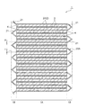
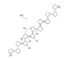
図1は第1実施形態に係るアクチュエータを示す概略断面図である。本実施形態に係るアクチュエータ1は、板状の負電極2と、メッシュ状の正電極3と、負電極2及び正電極3の間に挟まれた電気応答性樹脂層4とを、複数積層することにより形成されている。
<First Embodiment>
FIG. 1 is a schematic sectional view showing the actuator according to the first embodiment. The
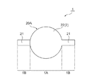
図2はアクチュエータ1の平面図である。平面視において、アクチュエータ1は、円形状の中央部1Aと、該中央部1Aの左右両側に延びる矩形状の縁部1Bとで形成されている。中央部1Aは、負電極2と正電極3と電気応答性樹脂層4とを積層する領域であり、縁部1Bは後述する電極部材20Aの連結耳部21を収める領域である。
FIG. 2 is a plan view of the
図1に示すように、負電極2は、一枚のシート状の電極部材20Aを積層方向に沿ってS字状に折り畳むことにより形成されている。電極部材20Aは、ステンレス材料からなり、積層方向に等間隔で配列された複数の電極部22と、隣接する電極部22同士を連結する連結耳部21とを有する。電極部22は、円形状に形成され、負電極2を構成する部分である。連結耳部21は、矩形状に形成され、隣接する電極部22同士の間に配置され、これらの電極部22を連結している。
As shown in FIG. 1, the
積層方向に隣接する電極部22同士は、これらを連結する連結耳部21の折り曲げによって互いに折り畳まれている。具体的には、連結耳部21は、その長さの略半分の場所で折り返されている。これによって、積層方向に隣接する電極部22同士を、位置ずれなく、向かい合わせている。
The
また、各電極部22において、電極部22に連結される連結耳部21は2箇所ずつあり、すなわち、上側の電極部22と連結するための連結耳部21、下側の電極部22と連結するための連結耳部21である。平面視で、2箇所に配置された連結耳部21は、電極部22の径方向に沿って電極部22から左右両側に延出しており、両者がなす角度は180°である(図2参照)。
Further, in each
積層方向に隣接する電極部22同士の間には、正電極3がその両側に設けられた電気応答性樹脂層4を介して挟持されている。正電極3は、ステンレス材料からなり、電極部22と同じ形状及び同じ大きさに形成されている。本実施形態において、負電極2及び正電極3には、ともにステンレス材料が用いられているが、ステンレスに代えて、導電性ゴムや導電性高分子組成物、銅等の金属材料が用いられてもよい。
Between the
電気応答性樹脂層4は、キャスト法、ディップコーティング法、スピンコート法、溶融コーティング法等で負電極2又は正電極3に直接形成されてもよく、又は別体として個別に作製されてもよい。ここで、電気応答性樹脂とは、電気に応答して変形挙動が起こる樹脂材料のことを意味し、例えば誘電エラストマーなどが挙げられる。そして、動作不良を防止するために、電気応答性樹脂層4の厚さは2mm以下が好ましい。これは、電気応答性樹脂層4の厚さが2mmを超えると、作動電圧が高くなり、短絡などによる動作不良が起こる可能性があるからである。
The electrically
以下、図3及び図4を参照しアクチュエータ1の製造方法を説明する。図3は、電極部材20Aを折り畳む前の状態、すなわち電極部材20Aの展開状態を示すものである。図3に示すように、負電極2の形成に用いられる電極部材20Aは、等間隔で直線状に配列された複数の電極部22と、電極部22の径方向に延びて隣接する電極部22同士を連結する複数の連結耳部21を有するように一体的に形成されている。
Hereinafter, the manufacturing method of the
そして、電極部22の最も幅広い部分の幅(すなわち、電極部22の直径)をL1、連結耳部21の幅をL2としたときに、電極部22の直径及び連結耳部21の幅は、L2≦L1/3の関係を満たすように設定されている。また、電極部材20Aの厚さをT、正電極3の厚さをtとしたときに、両者の厚さはT≦t/3の関係を満たすように設定されている。なお、本実施形態では、電極部22の直径L1が30mm、連結耳部21の幅L2が5mm、電極部材20Aの厚さTが10μm、正電極3の厚さtが50μmである。
When the width of the widest part of the electrode part 22 (that is, the diameter of the electrode part 22) is L1, and the width of the
このように電極部材20Aの厚さ、電極部22及び連結耳部21の幅を設定することで、電極部材20Aを折り畳む際に、連結耳部21の折り曲げにより生じる反発力の影響を抑制することができる。すなわち、外力を付与し連結耳部21を折り曲げると、連結耳部21が外力付与方向に弾性変形する。しかし、外力が解除されると、連結耳部21は反発変形(すなわち、スプリングバック)し、外力付与方向とは反対の方向に反発力が生じる。これによって、積層により電極部22と密着された電気応答性樹脂層4を、電極部22から引き離す力が働く。そして、上述の反発力が大きくなると、電極部22と電気応答性樹脂層4との間には、密着しない部分が発生して、アクチュエータ1の正常作動に悪影響を及ぼしてしまう。
In this way, by setting the thickness of the
上述の反発力を低減するために、連結耳部21の折り曲げで形成された角部にカーブを大きく付ける(例えば、曲げRを大きく取る)方法が考えられるが、カーブを大きく付けると、隣接する連結耳部21同士が接触し干渉するだけではなく、連結耳部21を収める空間が大きくなるので、アクチュエータのコンパクト化を実現し難くなる問題が新たに発生してしまう。これに対し、本実施形態では、上述のように電極部材20Aの厚さ、電極部22及び連結耳部21の幅を設定することで、スプリングバックによる反発力を低減することができると共に、アクチュエータ1のコンパクト化を実現し易くなる。なお、反発力を低減するために、許容できる範囲において、例えば連結耳部21の折り曲げ位置をできるだけ電極部22から遠い場所にしたり、又は連結耳部21を電極部22より薄くしたりすることも考えられる。
In order to reduce the above-described repulsive force, a method of enlarging a curve at a corner portion formed by bending the connecting ear portion 21 (for example, increasing the bending R) is conceivable. Not only does the connecting
図4はアクチュエータ1の製造方法を示す模式図である。アクチュエータ1を製造する際に、例えばまず、正電極3を個別に用意し、ディップコーティングを施すことで該正電極3の表裏両面に電気応答性樹脂層4を形成し、電極中間体5を複数作製する。ディップコーティングに用いるコーティング液は、電気応答性樹脂を溶媒に溶解したものである。
FIG. 4 is a schematic view showing a method for manufacturing the
次に、電極部材20Aを用意し、各連結耳部21の長さの半分の場所で該電極部材20Aを折り曲げて、隣接する電極部22同士の間に電極中間体5を順次に配置させる。隣接する電極部22同士の間に電極中間体5を全て配置させた後に、これらを積層することでアクチュエータ1を作製する。なお、上述の製造方法において、正電極3に代えて電極部材20Aにディップコーティングを施すことにより、該電極部材20Aの表裏両面に電気応答性樹脂層4を形成してもよい。
Next, an
本実施形態のアクチュエータ1では、負電極2は一枚の電極部材20Aを積層方向に沿ってS字状に折り畳むことにより形成され、積層方向に隣接する負電極2同士の間に、正電極3がその上下両側に設けられた電気応答性樹脂層4を介して挟持されている。従って、負電極2の両面を全て電極として利用することが可能にある。その結果、負電極2の電極面を有効に利用することができる。
In the
加えて、電極部材20Aにおいて、電極部22の直径L1と連結耳部21の幅L2とがL2≦L1/3の関係を満たし、電極部材20Aの厚さTと正電極3の厚さtとがT≦t/3の関係を満たすので、連結耳部21の折り曲げによる反発力を低減することができる。これによって、電極部22と電気応答性樹脂層4との間に密着しない部分の発生を確実に防止し、アクチュエータ1の正常作動を確保することができる。
In addition, in the
<第2実施形態>
図5は第2実施形態に係るアクチュエータを示す平面図である。本実施形態に係るアクチュエータ6と第1実施形態との相違点は、電極部22に連結される連結耳部23と、隣接する電極部22に連結される連結耳部23の連結耳部同士がなす角度が90°である点である。その他の構成は第1実施形態と同様のため、重複説明は省略する。
Second Embodiment
FIG. 5 is a plan view showing an actuator according to the second embodiment. The difference between the actuator 6 according to the present embodiment and the first embodiment is that the
図6は、負電極2の形成に用いられる電極部材20Bの展開状態を示す図である。電極部材20Bは、上述した電極部材20Aのように直線状に形成されておらず、一定の規則に沿って凹凸状に形成されている。具体的には、この電極部材20Bは、等間隔で配列された複数の電極部22と、電極部22の径方向に延びて隣接する電極部22同士を連結する複数の連結耳部23とを有するように一体的に形成されている。電極部材20Bは、これらの電極部22及び連結耳部23で、互いに平行する上下2段構成になっている。上段と下段では、それぞれ3つの電極部22が直線状に並設されている。また、上段と下段との距離は、連結耳部23の1本分の長さである。
FIG. 6 is a diagram illustrating a developed state of the electrode member 20 </ b> B used for forming the
このような構成を有する電極部材20Bを積層方向に沿ってS字状に折り畳むと、図5に示すように、連結耳部23は電極部22の円周に3箇所に分けて順次に配置されることになる。そして、各電極部22において、該電極部22に連結される連結耳部23と、隣接する電極部22に連結される連結耳部23の連結耳部同士がなす角度は90°である。このため、平面視で、3箇所に配置された連結耳部23は、90°の間隔で配置されている。
When the
図7はアクチュエータ6の製造方法を示す模式図である。アクチュエータ6を製造する際に、例えばまず、電気応答性樹脂層4を2層と正電極3を一枚それぞれ用意し、2層の電気応答性樹脂層4の間に正電極3を挟むようにこれらを積層して電極積層体7を複数作製する。次に、電極部材20Bを用意し、各連結耳部23の長さの半分の場所で連結耳部23を順次に折り曲げる。次に、隣接する電極部22同士の間に、電極積層体7を順次に配置させる。隣接する電極部22同士の間に電極積層体7を全て配置させた後に、これらを積層することでアクチュエータ6を作製する。
FIG. 7 is a schematic view showing a method for manufacturing the actuator 6. When manufacturing the actuator 6, for example, first, two electric
本実施形態のアクチュエータ6は、上述の第1実施形態と同様な作用効果を得られるほか、連結耳部23が電極部22の円周に沿って3箇所に分けて配置されるので、隣接する連結耳部23の折り曲げにより嵩張ることを抑制しつつ、隣接する連結耳部23同士の干渉を防止することができる。
The actuator 6 of the present embodiment can obtain the same effects as those of the first embodiment described above, and the
<第3実施形態>
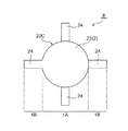
図8は第3実施形態に係るアクチュエータを示す平面図である。本実施形態に係るアクチュエータ8と第2実施形態との相違点は、連結耳部24が電極部22の円周に沿って4箇所に分けて配置されることである。
<Third Embodiment>
FIG. 8 is a plan view showing an actuator according to the third embodiment. The difference between the
図9は、負電極2の形成に用いられる電極部材20Cの展開状態を示す図である。電極部材20Cは、一定の規則に沿って階段状に形成されている。具体的には、この電極部材20Cは、等間隔で配列された複数の電極部22と、電極部22の径方向に延びて隣接する電極部22同士を連結する複数の連結耳部24とを有するように一体的に形成されている。各階段において、踏面にあたる部分と蹴上にあたる部分は、それぞれ2つの電極部22とこれらの電極部22を連結する連結耳部24によって構成されている。なお、踏面にあたる部分と蹴上にあたる部分は、互いに垂直になっている。
FIG. 9 is a diagram illustrating a developed state of the electrode member 20 </ b> C used for forming the
このような構成を有する電極部材20Cを積層方向に沿ってS字状に折り畳むと、図8に示すように、連結耳部24は、電極部22の円周に沿って90°の間隔で螺旋状に配置される。そして、各電極部22において、該電極部22に連結される連結耳部24と、隣接する電極部22に連結される連結耳部24の連結耳部同士がなす角度は90°である。本実施形態のアクチュエータ8は、第2実施形態のアクチュエータ6と同様な方法で製造することができる。ここでは、その説明を省略する。
When the
本実施形態のアクチュエータ8は、上述の第2実施形態と同様な作用効果を得られるほか、連結耳部24が電極部22の円周に沿って4箇所に分けて配置されるので、隣接する連結耳部24の折り曲げにより嵩張ることをより効果的に抑制することができ、隣接する連結耳部24同士の干渉を確実に防止することができる。
The
上述の第1〜第3実施形態において、負電極2のみに電極部材20A,20B,20Cを用いて形成する場合を説明したが、本発明はこれに限定されない。本発明は、正電極3のみに電極部材20A,20B,20Cを用いて形成する場合、負電極2及び正電極3双方にそれぞれ電極部材20A,20B,20Cを用いて形成する場合、負電極2と正電極3のいずれか一方の電極のみに複数の電極部材20A,20B,20Cを用いて形成する場合にも適用される。
In the first to third embodiments described above, the case where the
例えば、負電極2及び正電極3双方にそれぞれ電極部材20A,20B,20Cを用いて形成する場合には、電極部材20A,20B,20Cを2枚用意し、一枚を負電極2、他の一枚を正電極3とする。そして、負電極2としての電極部材20A,20B,20Cのみにディップコーティングを施し、該電極部材20A,20B,20Cの表裏両面に電気応答性樹脂層4を形成する。その後、正電極3としての電極部材20A,20B,20Cにおける隣接する電極部22同士の間に、負電極2としての電極部材20A,20B,20Cにおける電極部22を挟むように、これらの電極部材20A,20B,20Cを順次に折り畳んで積層することで、アクチュエータを作製することができる。
For example, when the
また、負電極2と正電極3のいずれか一方の電極(例えば、負電極2)のみに複数(ここでは、2枚)の電極部材20A,20B,20Cを用いて形成する場合には、まず、負電極2としての電極部材20A,20B,20Cを2枚用意する。次に、これらの2枚に対して、キャスト法で片面だけに電気応答性樹脂層4をそれぞれ形成させる。キャスト法に用いられる液は、例えば電気応答性樹脂を溶媒に溶解したものである。次に、電気応答性樹脂層4が形成されていない面同士を合わせるように、2枚の電極部材20A,20B,20Cを重ね合わせて、一体化させる。その後、一体化された電極部材20A,20B,20Cを順次に折り畳み、電気応答性樹脂層4が形成された面同士の間に、別体に用意された正電極3を挟み込んで積層することで、アクチュエータを作製することができる。
In addition, when forming a plurality of (here, two)
以上、本発明の実施形態について詳述したが、本発明は、上述の実施形態に限定されるものではなく、特許請求の範囲に記載された本発明の精神を逸脱しない範囲で、種々の設計変更を行うことができるものである。例えば、電極部22に連結される連結耳部21,23,24同士がなす角度は上述した内容に限らず、積層方向に隣接する連結耳部21,23,24同士の干渉を低減できる構造であれば、なす角度を変えてもよい。また、各電極の大きさ・電気応答性樹脂の大きさは必ずしも同一である必要はなく、例えば負電極と正電極の大きさが違ってもよいし、電気応答性樹脂の大きさが電極のそれよりも大きくても小さくてもよい。
Although the embodiments of the present invention have been described in detail above, the present invention is not limited to the above-described embodiments, and various designs can be made without departing from the spirit of the present invention described in the claims. It can be changed. For example, the angle formed between the
また、上記の実施形態では、負電極2(すなわち、電極部22)及び正電極3について円形状に形成される例を挙げて説明したが、これらの電極の形状を楕円形、他角形等としてもよい。更に、電極部材20A,20B,20Cについて、電極部22と連結耳部21,23,24共にステンレス材料により形成される例を説明したが、例えば電極部に銅、連結耳部にステンレスのように、部位によって材料を使い分けてもよい。
In the above embodiment, the negative electrode 2 (that is, the electrode portion 22) and the
また、負電極2及び正電極3の表面に機械的又は化学的加工を施してもよい。例えば、必要に応じて、負電極2及び正電極3の表面に梨地加工、掘り込み(メッシュ形状を含む)・溝切り加工を施してもよい。更に、電気応答性樹脂層4と負電極2、正電極3との密着性を高めるために、積層方向に圧縮効果をもたらす構造(例えば、ばね)を更にアクチュエータ1,6,8に取り付けてもよい。
Further, the surface of the
また、1つのアクチュエータ1,6,8において、上述の電極部材20A,20B,20Cを複数用いて直列又は並列に配置してもよい。直列に配置する場合、変形量の増大を期待できる。一方、並列に配置する場合、力の増加を期待できる。
Further, one
1,6,8 アクチュエータ
1A 中央部
1B 縁部
2 負電極
3 正電極
4 電気応答性樹脂層
5 電極中間体
7 電極積層体
20A,20B,20C 電極部材
21,23,24 連結耳部
22 電極部
1,6,8
Claims (2)
前記正電極及び前記負電極のうち、少なくとも一方の電極は、一枚の電極部材を積層方向に沿ってS字状に折り畳むことにより形成され、
積層方向に隣接する前記一方の電極同士の間には、他方の電極がその両側に設けられた前記電気応答性樹脂層を介して挟持されていることを特徴とするアクチュエータ。 An actuator formed by laminating a plurality of positive electrodes, negative electrodes, and electrically responsive resin layers sandwiched between these electrodes,
At least one of the positive electrode and the negative electrode is formed by folding one electrode member into an S shape along the stacking direction,
An actuator, wherein the other electrode is sandwiched between the one electrode adjacent in the stacking direction via the electrically responsive resin layer provided on both sides thereof.
隣接する前記電極部同士は、これらを連結する前記連結耳部の折り曲げによって互いに折り畳まれ、
各電極部において、該電極部に連結される前記連結耳部と、隣接する前記電極部に連結される前記連結耳部の連結耳部同士がなす角度は、180°以外であることを特徴とする請求項1に記載のアクチュエータ。 The electrode member has a plurality of electrode portions arranged at a predetermined interval, and a connecting ear portion that connects the adjacent electrode portions,
The adjacent electrode parts are folded together by bending of the connecting ear part connecting them,
In each electrode part, the angle formed by the connection ears of the connection ear part connected to the electrode part and the connection ear part connected to the adjacent electrode part is other than 180 °, The actuator according to claim 1.
Priority Applications (1)
| Application Number | Priority Date | Filing Date | Title |
|---|---|---|---|
| JP2016041241A JP2017158366A (en) | 2016-03-03 | 2016-03-03 | Actuator |
Applications Claiming Priority (1)
| Application Number | Priority Date | Filing Date | Title |
|---|---|---|---|
| JP2016041241A JP2017158366A (en) | 2016-03-03 | 2016-03-03 | Actuator |
Publications (1)
| Publication Number | Publication Date |
|---|---|
| JP2017158366A true JP2017158366A (en) | 2017-09-07 |
Family
ID=59810460
Family Applications (1)
| Application Number | Title | Priority Date | Filing Date |
|---|---|---|---|
| JP2016041241A Pending JP2017158366A (en) | 2016-03-03 | 2016-03-03 | Actuator |
Country Status (1)
| Country | Link |
|---|---|
| JP (1) | JP2017158366A (en) |
Cited By (1)
| Publication number | Priority date | Publication date | Assignee | Title |
|---|---|---|---|---|
| WO2020255977A1 (en) * | 2019-06-18 | 2020-12-24 | ストローブ株式会社 | Electrostatic actuator |
Citations (6)
| Publication number | Priority date | Publication date | Assignee | Title |
|---|---|---|---|---|
| JPS6388875A (en) * | 1986-10-01 | 1988-04-19 | Fuji Elelctrochem Co Ltd | Manufacture of laminated piezoelectric element |
| JPH07283455A (en) * | 1994-04-08 | 1995-10-27 | Oki Electric Ind Co Ltd | Method for manufacturing laminated piezoelectric element and electrode plate used for the same |
| JP2001268948A (en) * | 2000-03-21 | 2001-09-28 | Keiji Saneyoshi | Electrostatic actuator and operation mechanism using the same |
| JP2008211922A (en) * | 2007-02-27 | 2008-09-11 | Yamaha Corp | Polymer electrostatic actuator |
| JP2010057321A (en) * | 2008-08-29 | 2010-03-11 | Tokyo Institute Of Technology | Static actuator and manufacturing method therefor |
| JP2011103713A (en) * | 2009-11-10 | 2011-05-26 | Seiko Epson Corp | Actuator |
-
2016
- 2016-03-03 JP JP2016041241A patent/JP2017158366A/en active Pending
Patent Citations (6)
| Publication number | Priority date | Publication date | Assignee | Title |
|---|---|---|---|---|
| JPS6388875A (en) * | 1986-10-01 | 1988-04-19 | Fuji Elelctrochem Co Ltd | Manufacture of laminated piezoelectric element |
| JPH07283455A (en) * | 1994-04-08 | 1995-10-27 | Oki Electric Ind Co Ltd | Method for manufacturing laminated piezoelectric element and electrode plate used for the same |
| JP2001268948A (en) * | 2000-03-21 | 2001-09-28 | Keiji Saneyoshi | Electrostatic actuator and operation mechanism using the same |
| JP2008211922A (en) * | 2007-02-27 | 2008-09-11 | Yamaha Corp | Polymer electrostatic actuator |
| JP2010057321A (en) * | 2008-08-29 | 2010-03-11 | Tokyo Institute Of Technology | Static actuator and manufacturing method therefor |
| JP2011103713A (en) * | 2009-11-10 | 2011-05-26 | Seiko Epson Corp | Actuator |
Cited By (2)
| Publication number | Priority date | Publication date | Assignee | Title |
|---|---|---|---|---|
| WO2020255977A1 (en) * | 2019-06-18 | 2020-12-24 | ストローブ株式会社 | Electrostatic actuator |
| US11848625B2 (en) | 2019-06-18 | 2023-12-19 | Strawb Inc. | Electrostatic actuator |
Similar Documents
| Publication | Publication Date | Title |
|---|---|---|
| JP6557346B2 (en) | Secondary battery electrode assembly and manufacturing method thereof | |
| US9172109B2 (en) | Electrode assembly and secondary battery using the same | |
| JP5625899B2 (en) | battery | |
| JP6879492B2 (en) | Electrode assembly and its manufacturing method | |
| JP2015513196A (en) | Electrode assembly having a step including a step unit cell | |
| JP5267363B2 (en) | Multilayer electronic components | |
| US11393972B2 (en) | Multi-layer piezoelectric ceramic component and piezoelectric device | |
| JP5929279B2 (en) | Multilayer capacitor | |
| JPWO2017068709A1 (en) | Assembled battery | |
| JP2015159086A (en) | power storage device | |
| JP2013187104A (en) | Battery module, and flat battery cell | |
| JP2008211922A (en) | Polymer electrostatic actuator | |
| JP2017158366A (en) | Actuator | |
| JP2011108785A (en) | Stacked capacitor | |
| JP6274011B2 (en) | Power storage device | |
| JP4747574B2 (en) | Assembled battery | |
| JP7045587B2 (en) | Secondary battery | |
| JP5499620B2 (en) | Actuator and method of manufacturing actuator | |
| CN111490216B (en) | Battery module | |
| JP6119385B2 (en) | Battery module | |
| JP7601167B2 (en) | Battery module manufacturing method | |
| JP7038957B2 (en) | Manufacturing method of battery cell and electrode lead | |
| JP2011172404A (en) | Static actuator, and manufacturing method therefor | |
| WO2017038137A1 (en) | Capacitor element | |
| JP4977356B2 (en) | Electrical device assembly |
Legal Events
| Date | Code | Title | Description |
|---|---|---|---|
| A621 | Written request for application examination |
Free format text: JAPANESE INTERMEDIATE CODE: A621 Effective date: 20180417 |
|
| A977 | Report on retrieval |
Free format text: JAPANESE INTERMEDIATE CODE: A971007 Effective date: 20190125 |
|
| A131 | Notification of reasons for refusal |
Free format text: JAPANESE INTERMEDIATE CODE: A131 Effective date: 20190205 |
|
| A521 | Request for written amendment filed |
Free format text: JAPANESE INTERMEDIATE CODE: A523 Effective date: 20190327 |
|
| A02 | Decision of refusal |
Free format text: JAPANESE INTERMEDIATE CODE: A02 Effective date: 20190827 |