JP2017123209A - Thin plate wiring board and manufacturing method of the same - Google Patents
Thin plate wiring board and manufacturing method of the same Download PDFInfo
- Publication number
- JP2017123209A JP2017123209A JP2016002021A JP2016002021A JP2017123209A JP 2017123209 A JP2017123209 A JP 2017123209A JP 2016002021 A JP2016002021 A JP 2016002021A JP 2016002021 A JP2016002021 A JP 2016002021A JP 2017123209 A JP2017123209 A JP 2017123209A
- Authority
- JP
- Japan
- Prior art keywords
- terminal
- layer
- modification
- insulating layer
- solder
- Prior art date
- Legal status (The legal status is an assumption and is not a legal conclusion. Google has not performed a legal analysis and makes no representation as to the accuracy of the status listed.)
- Granted
Links
- 238000004519 manufacturing process Methods 0.000 title description 9
- 230000004888 barrier function Effects 0.000 claims abstract description 158
- 229910000679 solder Inorganic materials 0.000 claims abstract description 137
- 239000002184 metal Substances 0.000 claims abstract description 59
- 229910052751 metal Inorganic materials 0.000 claims abstract description 59
- 239000000758 substrate Substances 0.000 claims abstract description 27
- 239000000463 material Substances 0.000 claims abstract description 24
- 238000009413 insulation Methods 0.000 abstract description 11
- 230000001629 suppression Effects 0.000 abstract 1
- 239000010410 layer Substances 0.000 description 368
- 230000004048 modification Effects 0.000 description 186
- 238000012986 modification Methods 0.000 description 186
- RYGMFSIKBFXOCR-UHFFFAOYSA-N Copper Chemical compound [Cu] RYGMFSIKBFXOCR-UHFFFAOYSA-N 0.000 description 39
- 229910052802 copper Inorganic materials 0.000 description 39
- 239000010949 copper Substances 0.000 description 39
- 238000005530 etching Methods 0.000 description 30
- 230000000694 effects Effects 0.000 description 24
- 238000000034 method Methods 0.000 description 17
- 238000007747 plating Methods 0.000 description 16
- 239000000725 suspension Substances 0.000 description 16
- PCHJSUWPFVWCPO-UHFFFAOYSA-N gold Chemical compound [Au] PCHJSUWPFVWCPO-UHFFFAOYSA-N 0.000 description 13
- 239000010931 gold Substances 0.000 description 13
- 229910052737 gold Inorganic materials 0.000 description 13
- 239000000654 additive Substances 0.000 description 11
- 239000002355 dual-layer Substances 0.000 description 9
- 238000005304 joining Methods 0.000 description 8
- 238000013532 laser treatment Methods 0.000 description 6
- PXHVJJICTQNCMI-UHFFFAOYSA-N Nickel Chemical compound [Ni] PXHVJJICTQNCMI-UHFFFAOYSA-N 0.000 description 4
- 230000015572 biosynthetic process Effects 0.000 description 4
- 230000008569 process Effects 0.000 description 4
- 239000004642 Polyimide Substances 0.000 description 3
- 230000009471 action Effects 0.000 description 3
- 238000005452 bending Methods 0.000 description 3
- 239000011810 insulating material Substances 0.000 description 3
- 229920001721 polyimide Polymers 0.000 description 3
- 229910001220 stainless steel Inorganic materials 0.000 description 3
- 239000010935 stainless steel Substances 0.000 description 3
- 230000008878 coupling Effects 0.000 description 2
- 238000010168 coupling process Methods 0.000 description 2
- 238000005859 coupling reaction Methods 0.000 description 2
- 238000010586 diagram Methods 0.000 description 2
- 238000010329 laser etching Methods 0.000 description 2
- 230000000873 masking effect Effects 0.000 description 2
- 229910052759 nickel Inorganic materials 0.000 description 2
- 230000001105 regulatory effect Effects 0.000 description 2
- 229910000963 austenitic stainless steel Inorganic materials 0.000 description 1
- 239000004020 conductor Substances 0.000 description 1
- 230000007423 decrease Effects 0.000 description 1
- 239000012777 electrically insulating material Substances 0.000 description 1
- 230000008030 elimination Effects 0.000 description 1
- 238000003379 elimination reaction Methods 0.000 description 1
- 230000010365 information processing Effects 0.000 description 1
- 239000004033 plastic Substances 0.000 description 1
- 230000009467 reduction Effects 0.000 description 1
- 239000002356 single layer Substances 0.000 description 1
- 239000010409 thin film Substances 0.000 description 1
- 238000003466 welding Methods 0.000 description 1
Images


Classifications
-
- H—ELECTRICITY
- H05—ELECTRIC TECHNIQUES NOT OTHERWISE PROVIDED FOR
- H05K—PRINTED CIRCUITS; CASINGS OR CONSTRUCTIONAL DETAILS OF ELECTRIC APPARATUS; MANUFACTURE OF ASSEMBLAGES OF ELECTRICAL COMPONENTS
- H05K3/00—Apparatus or processes for manufacturing printed circuits
- H05K3/36—Assembling printed circuits with other printed circuits
- H05K3/361—Assembling flexible printed circuits with other printed circuits
- H05K3/363—Assembling flexible printed circuits with other printed circuits by soldering
-
- H—ELECTRICITY
- H05—ELECTRIC TECHNIQUES NOT OTHERWISE PROVIDED FOR
- H05K—PRINTED CIRCUITS; CASINGS OR CONSTRUCTIONAL DETAILS OF ELECTRIC APPARATUS; MANUFACTURE OF ASSEMBLAGES OF ELECTRICAL COMPONENTS
- H05K1/00—Printed circuits
- H05K1/02—Details
- H05K1/03—Use of materials for the substrate
- H05K1/05—Insulated conductive substrates, e.g. insulated metal substrate
-
- H—ELECTRICITY
- H05—ELECTRIC TECHNIQUES NOT OTHERWISE PROVIDED FOR
- H05K—PRINTED CIRCUITS; CASINGS OR CONSTRUCTIONAL DETAILS OF ELECTRIC APPARATUS; MANUFACTURE OF ASSEMBLAGES OF ELECTRICAL COMPONENTS
- H05K1/00—Printed circuits
- H05K1/02—Details
- H05K1/03—Use of materials for the substrate
- H05K1/0393—Flexible materials
-
- H—ELECTRICITY
- H05—ELECTRIC TECHNIQUES NOT OTHERWISE PROVIDED FOR
- H05K—PRINTED CIRCUITS; CASINGS OR CONSTRUCTIONAL DETAILS OF ELECTRIC APPARATUS; MANUFACTURE OF ASSEMBLAGES OF ELECTRICAL COMPONENTS
- H05K1/00—Printed circuits
- H05K1/02—Details
- H05K1/03—Use of materials for the substrate
- H05K1/05—Insulated conductive substrates, e.g. insulated metal substrate
- H05K1/056—Insulated conductive substrates, e.g. insulated metal substrate the metal substrate being covered by an organic insulating layer
-
- H—ELECTRICITY
- H05—ELECTRIC TECHNIQUES NOT OTHERWISE PROVIDED FOR
- H05K—PRINTED CIRCUITS; CASINGS OR CONSTRUCTIONAL DETAILS OF ELECTRIC APPARATUS; MANUFACTURE OF ASSEMBLAGES OF ELECTRICAL COMPONENTS
- H05K2201/00—Indexing scheme relating to printed circuits covered by H05K1/00
- H05K2201/05—Flexible printed circuits [FPCs]
- H05K2201/058—Direct connection between two or more FPCs or between flexible parts of rigid PCBs
-
- H—ELECTRICITY
- H05—ELECTRIC TECHNIQUES NOT OTHERWISE PROVIDED FOR
- H05K—PRINTED CIRCUITS; CASINGS OR CONSTRUCTIONAL DETAILS OF ELECTRIC APPARATUS; MANUFACTURE OF ASSEMBLAGES OF ELECTRICAL COMPONENTS
- H05K2201/00—Indexing scheme relating to printed circuits covered by H05K1/00
- H05K2201/09—Shape and layout
- H05K2201/09818—Shape or layout details not covered by a single group of H05K2201/09009 - H05K2201/09809
- H05K2201/09909—Special local insulating pattern, e.g. as dam around component
Landscapes
- Engineering & Computer Science (AREA)
- Microelectronics & Electronic Packaging (AREA)
- Manufacturing & Machinery (AREA)
- Supporting Of Heads In Record-Carrier Devices (AREA)
- Adjustment Of The Magnetic Head Position Track Following On Tapes (AREA)
Abstract
Description
本発明は、ヘッドサスペンションのフレキシャー等に適用され薄板配線基板及びその製造方法に関する。 The present invention relates to a thin wiring board applied to a flexure or the like of a head suspension and a manufacturing method thereof.
パーソナルコンピュータ等の情報処理装置に、ハードディスクドライブ(HDD)が使用されている。ハードディスクドライブは、スピンドルを中心に回転する磁気ディスクと、ピボット軸を中心に旋回するキャリッジなどを含んでいる。キャリッジのアームに、ディスク装置用ヘッドサスペンション(以下、単に「ヘッドサスペンション」と称する。)が設けられている。 A hard disk drive (HDD) is used in an information processing apparatus such as a personal computer. The hard disk drive includes a magnetic disk that rotates about a spindle and a carriage that rotates about a pivot shaft. A disk device head suspension (hereinafter simply referred to as “head suspension”) is provided on the arm of the carriage.
特許文献1の記載のように、ヘッドサスペンションは、ロードビーム(load beam)と、ロードビームに重ねて配置されるフレキシャー (flexure)などを有している。フレキシャーの先端付近に形成されたジンバル部にスライダーを含む磁気ヘッドが取付けられている。磁気ヘッドには、データの読取りあるいは書込み等のアクセスを行なうための素子が設けられている。これらヘッドサスペンション及びフレキシャーなどによってヘッドジンバルアセンブリが構成されている。 As described in Patent Document 1, the head suspension includes a load beam, a flexure disposed so as to overlap the load beam, and the like. A magnetic head including a slider is attached to a gimbal portion formed near the tip of the flexure. The magnetic head is provided with an element for performing access such as data reading or writing. A head gimbal assembly is constituted by the head suspension and the flexure.
フレキシャーは、要求される仕様に応じて様々な形態のものが実用化されている。その一例として、薄板配線基板としての配線付フレキシャー (flexure with conductors)(以下の説明においては、「配線付フレキシャー」を「フレキシャー」という。)が知られている。フレキシャーは、薄いステンレス鋼板からなる金属支持層と、この金属支持層上に形成されたポリイミド等の電気絶縁材料からなるベース絶縁層と、このベース絶縁層の表面に複数本の配線として配索された配線層などを含んでいる。フレキシャーは、ロードビームに重なる本体部と、ベースプレートの後方に延出するテール部とを含んでいる。 Various types of flexures have been put to practical use according to required specifications. As one example, flexure with conductors (in the following description, “flexure with wiring” is known as “flexure”) as a thin wiring board is known. The flexure is routed as a metal support layer made of a thin stainless steel plate, a base insulation layer made of an electrically insulating material such as polyimide formed on the metal support layer, and a plurality of wires on the surface of the base insulation layer. Wiring layer etc. are included. The flexure includes a main body that overlaps the load beam and a tail that extends rearward of the base plate.
複数本の配線の一部は書込用であり、配線の他の一部は読取用であるのが基本的な構成である。これら配線の一端は、磁気ヘッドに設けられた素子、例えばMR(Magneto Resistive)素子に接続されている。配線の他端は、フレキシャーのテールパッド部に形成された複数のテール端子部に接続されている。これらテール端子部は、FPC(Flexible Printed Circuit board)等の回路基板の複数の基板端子部に対応して電気的に接合される。回路基板にはプリアンプ等の信号処理回路が実装されている。 The basic configuration is that a part of the plurality of wirings is for writing and the other part of the wirings is for reading. One end of these wirings is connected to an element provided in the magnetic head, for example, an MR (Magneto Resistive) element. The other end of the wiring is connected to a plurality of tail terminal portions formed on the tail pad portion of the flexure. These tail terminal portions are electrically joined to correspond to a plurality of substrate terminal portions of a circuit board such as an FPC (Flexible Printed Circuit board). A signal processing circuit such as a preamplifier is mounted on the circuit board.
そして、特許文献1のテール端子部の複数の端子部は、回路基板の複数の端子部に重ねられ、超音波接合等のボンディング手段によって接合されている。 And the several terminal part of the tail terminal part of patent document 1 is piled up on the several terminal part of a circuit board, and is joined by bonding means, such as ultrasonic bonding.
これに対し、接続信頼性を考慮し、超音波接合等に代えてはんだ接合を用いるものがある。この場合、複数のテール端子部を、マイクロはんだボールを介して基板の複数の基板端子部に重ね、リフローで両端止部をはんだ接合する。 On the other hand, in consideration of connection reliability, some solder joints are used instead of ultrasonic joining or the like. In this case, the plurality of tail terminal portions are overlapped with the plurality of substrate terminal portions of the substrate via the micro solder balls, and both end stoppers are soldered by reflow.
しかし、この構造では、所謂はんだブリッジ(=短絡発生)が問題となる。 However, in this structure, a so-called solder bridge (= short circuit occurrence) becomes a problem.
さらに述べると、ヘッドサスペンションの多機能化による多配線化に伴い、他部品である回路基板との接続に用いる端子部の数も増加している。加えてハードディスクドライブの小型化も進み、テールパッド部でのテール端子部全体が占めるスペースにも限界が有り、おのずと端子部間距離が減少する。この端子部間距離の減少は、はんだブリッジを多発させる原因となり、その対策が求められている。 More specifically, the number of terminal portions used for connection to circuit boards, which are other components, has increased with the increase in the number of wirings due to the multifunctional head suspension. In addition, miniaturization of hard disk drives has progressed, and there is a limit to the space occupied by the entire tail terminal part in the tail pad part, which naturally reduces the distance between the terminal parts. This reduction in the distance between the terminal portions causes frequent occurrence of solder bridges, and countermeasures are required.
この場合、マイクロはんだボールの径をより小さくすることではんだブリッジを抑制できるが、はんだフィレットが十分な大きさにならないという問題を招く。 In this case, the solder bridge can be suppressed by making the diameter of the micro solder ball smaller, but this causes a problem that the solder fillet is not sufficiently large.
解決しようとする問題点は、ヘッドサスペンションの多機能化、或いはハードディスクドライブの小型化などに伴い、端子間距離が減少し、はんだブリッジを多発させる原因となるのに対し、マイクロはんだボールの径を小さくすることではんだブリッジを抑制できるが、はんだフィレットが十分な大きさにならない点である。 The problem to be solved is that the distance between the terminals decreases as the head suspension becomes more multifunctional or the hard disk drive becomes smaller. Although solder bridges can be suppressed by reducing the size, the solder fillet is not sufficiently large.
本発明は、端子間距離が減少しても、はんだブリッジの発生を抑制しつつ十分な大きさのはんだフィレットを得ることを可能とするため、基板をなす金属性の金属支持層と、前記金属支持層の表面に備えられた絶縁性のベース絶縁層と、前記ベース絶縁層の表面に複数本の配線として配索された配線層と、前記配線を被覆する絶縁性のカバー絶縁層と、前記複数の配線に備えられ連続的に隣接配置された複数の端子部とを備え、前記複数の端子部が対応する複数の外部端子にそれぞれはんだ材によりはんだ接合される薄板配線基板であって、前記端子部が、前記はんだ材に対する障壁部を少なくとも前記端子部間に備えたことを薄板配線基板の特徴とする。 The present invention makes it possible to obtain a sufficiently large solder fillet while suppressing the occurrence of solder bridges even when the distance between terminals is reduced. An insulating base insulating layer provided on the surface of the support layer; a wiring layer arranged as a plurality of wires on the surface of the base insulating layer; an insulating cover insulating layer covering the wiring; A plurality of terminal portions that are provided in a plurality of wirings and continuously adjacent to each other, wherein the plurality of terminal portions are respectively solder-bonded to a plurality of corresponding external terminals by a solder material, A feature of the thin wiring board is that the terminal portion includes at least a barrier portion for the solder material between the terminal portions.
本発明の薄板配線基板は、上記構成であるから、はんだ接合時にリフローされたはんだ材の流れを障壁部が規制するので、はんだ材が端子部間を短絡するはんだブリッジを抑制できる。 Since the thin wiring board of the present invention has the above-described configuration, the barrier portion regulates the flow of the solder material reflowed at the time of solder joining, so that it is possible to suppress a solder bridge in which the solder material short-circuits between the terminal portions.
また、障壁部間の凹部がはんだ溜まりとなり、十分な大きさのはんだフィレットを形成することができる。 Moreover, the recessed part between barrier parts becomes a solder pool, and a sufficiently large solder fillet can be formed.
端子間距離が減少しても、はんだブリッジの発生を抑制しつつ十分な大きさのはんだフィレットを得ることを可能にするという目的を、本発明に係る薄板配線基板は、はんだ材に対する障壁部を連続的に隣接配置された複数の端子部の少なくとも端子部間に備えたことで実現した。 The purpose of the present invention is to provide a sufficiently large solder fillet while suppressing the occurrence of solder bridges even when the distance between terminals is reduced. This is realized by providing at least between terminal portions of a plurality of terminal portions arranged adjacent to each other.
前記障壁部は、前記端子部の中央部を周回状に囲んではんだ溜まり凹部を形成してもよい。 The barrier portion may surround the central portion of the terminal portion in a circular shape to form a solder pool recess.
前記障壁部は、前記ベース絶縁層と前記配線層とに薄層部又は孔を選択的に備えることによって設けてもよい。 The barrier portion may be provided by selectively providing a thin layer portion or a hole in the base insulating layer and the wiring layer.
前記障壁部を、前記ベース絶縁層と前記配線層とに渡って形成され前記金属支持層に接地されたグランドに設けてもよい。 The barrier portion may be provided on a ground formed across the base insulating layer and the wiring layer and grounded to the metal support layer.
図1〜5は、本発明の実施例を理解するための第1参考例、図6〜10は、同第2参考例である。本発明の薄板配線基板である実施例のフレキシャーの構造、機能の理解の前提として、第1、第2参考例によりハードディスクドライブ及びフレキシャーを取り付けたヘッドサスペンションとの関連を先に説明する。 1 to 5 are a first reference example for understanding an embodiment of the present invention, and FIGS. 6 to 10 are a second reference example. As a premise for understanding the structure and function of the flexure of the embodiment which is the thin wiring board of the present invention, the relationship between the hard disk drive and the head suspension attached with the flexure according to the first and second reference examples will be described first.
[第1参考例]
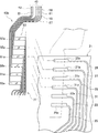
図1は、ハードディスクドライブの概略斜視図である。図1のハードディスクドライブ1は、ケース3と、スピンドル5を中心に回転するディスク7と、ピボット軸9を中心に旋回可能なキャリッジ11と、キャリッジ11を駆動するためのポジショニング用モータ13などを有している。ケース3は、蓋(図示せず)によって密閉される。
[First Reference Example]
FIG. 1 is a schematic perspective view of a hard disk drive. The hard disk drive 1 shown in FIG. 1 has a
図2は、ハードディスクドライブの一部を示す概略断面図である。この図2のように、キャリッジ11にアーム15が設けられている。アーム15の先端部に、ヘッドサスペンション17が取付けられている。ヘッドサスペンション17の先端に、磁気ヘッドとして機能するスライダー19が設けられている。ディスク7が高速で回転すると、ディスク7とスライダー19との間にエアベアリングが形成される。
FIG. 2 is a schematic sectional view showing a part of the hard disk drive. As shown in FIG. 2, an
ポジショニング用モータ13によってキャリッジ11が旋回すると、ヘッドサスペンション17がディスク7の径方向に移動することにより、スライダー19がディスク7の所望トラックまで移動する。スライダー19には、ディスク7にデータを記録するための磁気コイルと、ディスク7に記録されたデータを読取るためのMR素子と、ヒーターとなどが設けられている。MR素子は磁気信号と電気信号とを変換するための読取り手段として機能する。
When the
図3は、フレキシャーを取り付けたヘッドサスペンションと回路基板との概略平面図である。 FIG. 3 is a schematic plan view of the head suspension to which the flexure is attached and the circuit board.
図3のように、回路基板21の一例はFPCである。回路基板21に、書込用の配線23,25と、読取用の配線27、29と、ヒーター用の配線31と、グランド用の配線33とが設けられている。これら配線23、25、27、29、31、33の基板端子部23a、25a、27a、29a、31a、33aは、回路基板21の表面に露出している。
As shown in FIG. 3, an example of the
回路基板21には、信号処理回路の一部をなすプリアンプ35(図1に示す)が実装されている。プリアンプ35は、書込用の配線23,25と読取用の配線27、29に接続されている。プリアンプ35から出力される書込用の電流は、書込用の配線23,25を介してスライダー19の磁気コイルに供給される。スライダー19に設けられたMR素子から出力される電気信号は、読取用の配線27、29を介してプリアンプ35に入力される。書込用の配線23,25には、読取用の配線27、29よりも大きな電流が流れる。
A preamplifier 35 (shown in FIG. 1) forming a part of the signal processing circuit is mounted on the
ヘッドサスペンション17は、ベースプレート37と、ロードビーム39と、ヒンジ部材41と、フレキシャー 43などを備えている。ベースプレート37のボス部37aは、キャリッジ11のアーム15(図1、図2参照)に固定されている。フレキシャー43の先端付近にタング45(図3に示す)が形成されている。タング45にスライダー19が取付けられている。
The
フレキシャー43は、ロードビーム39に沿う本体部43aと、本体部43aからベースプレート37の後方に延びるテール部43bとを含んでいる。なお、ベースプレート37の後方とは、図3において矢印Rで示す方向、すなわち回路基板21に近付く方向である。フレキシャー43の本体部43aは、レーザー溶接等の固定手段によってロードビーム39に固定されている。
The
図4は、回路基板とフレキシャーのテールパッド部と回路基板とを接合した状態の要部拡大平面図、図5は、フレキシャーのテールパッド部と回路基板とを接合前の分離した状態で示す要部拡大平面図である。 FIG. 4 is an enlarged plan view of a main part in a state where the circuit board, the tail pad portion of the flexure and the circuit board are joined, and FIG. 5 is a diagram showing a state where the tail pad portion of the flexure and the circuit board are separated before joining. FIG.
フレキシャー43は、例えばオーステナイト系ステンレス鋼の板からなるメタルベースとなる金属支持層47と、金属支持層47に沿って形成された配線部49とを含んでいる。金属支持層47は曲げ加工等の塑性加工が可能であり、かつ、ばね性を有している。金属支持層47の厚さはロードビーム39の厚さよりも小さい。ロードビーム39の厚さは例えば30〜62μm、金属支持層47の厚さは例えば18μm(12〜25μm)である。
The
配線部49は、金属支持層47上に形成されたベース絶縁層と、ベース絶縁層の表面に配索された書込用の配線51、53と、読取用の配線55、57と、ヒーター用の配線59と、グランド用の配線61と、これらの配線51、53、55、57、59、61を覆うカバー絶縁層とを含んでいる。
The
図4と図5に示されるように、テール部43bにテールパッド部63が形成されている。テールパッド部63に、書込用のテール端子部51a、53aと、読取用のテール端子部55、57aと、ヒーター用のテール端子部59aと、グランド用のテール端子部61aが配置されている。
As shown in FIGS. 4 and 5, a
テール端子部51a、53a、55a、57a、59a、61aは、テールパッド部63において、互いに略平行となるように隣接配置されている。テール端子部51a、53a、55a、57a、59a、61aが回路基板21の基板端子部23a、25a、27a、29a、31a、33aに重ねられ、超音波接合等のボンディング手段によって接合されている。
The
テールパッド部63の金属支持層47には、開口65を有する枠部67が形成されている。開口65はテール部43bの長手方向(図4に矢印Z1で示す)に延びている。金属支持層47の開口65は、エッチングによって形成されている。ベース絶縁層とカバー絶縁層にも同様の開口65が形成されている。テール端子部51a、53a、55a、57a、59a、61aはそれぞれ開口65を横断し、開口65の内側において露出している。
A
開口65は、テール部43bの長手方向(図4に矢印Z1で示す)に延びる縦枠69、71と、テール部43bの幅方向(図4に矢印Z2で示す)に延びる横枠73、75とからなる。すなわち縦枠69、71と横枠73、75とによって枠部67が構成されている。縦枠69、71と横枠73、75とは、いずれも金属支持層47の一部である。
The
なお、第1参考例では、テスト用パッド部が切離された後に残るスタブ77が示されている。
In the first reference example, a
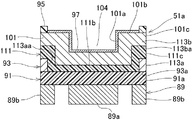
[第2参考例]
図6〜図10は、上記テールパッド部に代えて、ヘッドサスペンション17の多機能化による多配線化に伴い、回路基板との接続に用いるテール端子部の数もさらに増加したテールパッド部を示す。図6は、フレキシャーのテール端子部を示す要部拡大平面図である。図7は、フレキシャーのテール端子部を示す要部拡大裏面図である。図8は、フレキシャーのテール端子部の一部を示す要部拡大平面図である。図9は、図8のA−A線矢視において基板端子部との結合関係で示す要部拡大断面図である。図10は、図8のB−B線矢視において基板端子部との結合関係で示す要部拡大断面図である。なお、説明には上記第1参考例と同一の符号を用い、重複説明は省略する。図6〜図10の説明において存在しない符号は、第1参考例を参照する。
[Second Reference Example]
6 to 10 show a tail pad portion in which the number of tail terminal portions used for connection to the circuit board is further increased in accordance with the increase in the number of wirings due to the multifunction of the
図6、図7のように、第2参考例のテール端子部51a、53a、55a、57a、59a、61a、79a、81a、83a、85aは、図3の第1参考例のテール端子部51a、53a、55a、57a、59a、61aよりも端子数を増加させ、多機能に応じた構造となっている。
As shown in FIGS. 6 and 7, the
第2参考例のテール端子部51a、53a、55a、57a、59a、61a、79a、81a、83a、85aも複数の配線に備えられている。テール端子部51a、・・・は、テールパッド部63において、開口65を横断するように互いに略平行となるように連続的に隣接配置されている。連続的な隣接配置は、等間隔で行なわれているが、一部などを異なる間隔で隣接配置させることもできる。開口65の形状は、テール部43bの長手方向の両端等において図4の第1参考例と多少異なるが、開口の機能としては異なることは無い。
The
第2参考例のテール端子部51a、53a、55a、57a、59a、61a、79a、81a、83a、85aが開口65において形成する隣接方向(テールパッド部63の長手方向)の間隔は、端子数の増加により第1参考例に比較しても明らかなように、益々小さくなっている。
In the second reference example, the
ここで、テール端子部51a、53a、55a、57a、59a、61a、79a、81a、83a、85aは、配線部49の端末部を構成するものであり、その積層構造は、第1参考例の配線部49に対応している。
Here, the
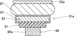
図8、図9、図10で示すテール端子部51aについて説明する。他のテール端子部53a、55a、57a、59a、61a、79a、81a、83a、85aも略同様な積層構造である。なお、グランドとなる例えばテール端子部85aは、グランドのための構造をさらに備える。
The
テール端子部51aは、端子部金属支持層89の表面に備えられた端子部ベース絶縁層91と、端子部ベース絶縁層91の表面に形成された端子層93と、端子部カバー絶縁層95と、端子層93を覆う金メッキ97とからなっている。金メッキ97は、下地にニッケルメッキを施す場合もある。
The
端子部金属支持層89は、基板をなす金属性の金属支持層である。この端子部金属支持層89は、1参考例の金属支持層47(図4、図5参照。)に形成されて金属支持層47に含まれ、材質、厚みは、第1参考例の金属支持層47の材質、厚みと同様である。テール端子部51aでの端子部金属支持層89は、中央に島状部89aを備えている。
図9をA−A線断面、図10をB−B線断面と称すると、A−A線断面では、端子面がフラットである。B−B線断面では、端子部カバー絶縁層95及び金メッキ97の厚み設定によりテール端子部51aの中央部の端子面が両側の端子部カバー絶縁層95に対して若干凹んだ形態となる。
The terminal
When FIG. 9 is referred to as an AA line cross section and FIG. 10 is referred to as a BB line cross section, the terminal surface is flat in the AA line cross section. In the cross section taken along the line BB, the terminal surface at the center of the
図10で示すB−B線断面では、島状部89aの幅が、図9で示すA−A線断面よりも大きく、且つ両側に離間した側壁部89bを備えている。これら島状部89a及び側壁部89bは、テール端子部51aの補強のために形成されている。島状部89a及び側壁部89bは、配線部49の金属支持層47に含まれ、側壁部89bは、金属支持層47(図4参照。)に一体となっている。
In the cross section taken along line BB shown in FIG. 10, the width of the island-shaped
端子部ベース絶縁層91及び端子部カバー絶縁層95は、第1参考例の配線部49(図4参照。)のものと同様であり、ポリイミド等の絶縁性の電気絶縁性材で形成され、端子部ベース絶縁層91の厚みは、例えば10μm(5〜20μm)に設定されている。端子部カバー絶縁層95の厚みは、例えば5μm(2〜10μm)に設定されている。
The terminal portion
端子層93は、配線51(図4、図5参照。)に含まれて配線51の端末をなす。配線51は、他の配線と共に複数本の配線として配索された配線層99(図6参照。)を構成している。端子層93は、銅メッキにより形成され、その厚みは、例えば10μm(4〜15μm)に設定されている。この端子層93は、B−B線断面において端子面の両側が前記端子部カバー絶縁層95により被覆されている。
金メッキ97は、表面薄膜層として形成され、金メッキ97の厚みは、例えば0.5μm(0.1〜5.0μm)に設定されている。
The
The
第2参考例では、図9、図10で示すテール端子部51aと基板端子部23aとの接合に示すように、テール端子部51a、53a、55a、57a、59a、61a、79a、81a、83a、85aと外部端子である回路基板の基板端子部23a、・・・とが対応して重ねられ、接合される。なお、回路基板の基板端子部23a、・・・は、第1、第2参考例よりも増加し、実施例1のテール端子部51a、・・・に対応した数を備えている。
In the second reference example, the
この接合は、第1参考例の超音波接合等のボンディング手段に代え、マイクロはんだボールを使用したリフローにより、はんだフィレット87を形成してはんだ接合し、接続信頼性を向上させている。
In this joining, instead of the bonding means such as the ultrasonic joining of the first reference example,
一方、特にテール端子部51a、53a、55a、57a、59a、61a、79a、81a、83a、85aが連続して隣接する図9のA−A線断面では、端子面がフラットであり、且つ端子間距離が第1、第2参考例に比較して狭くなっている。
このため、同じような大きさのマイクロはんだボールを用い、テール端子部51a、・・・と基板端子部23a、・・・とを規定間隔に押し付けてリフローさせると、溶融したはんだ材が大きく流れ出し、テール端子部51a、・・・の何れかの間、或いは全ての間で、はんだブリッジの発生を招く恐れがある。
On the other hand, in particular, in the cross-section taken along the line AA in FIG. The distance between them is narrower than in the first and second reference examples.
For this reason, when micro solder balls of the same size are used and the
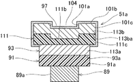
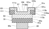
[障壁部]
図11、図12は、障壁部を備えた実施例1に係るものである。図11は、図9同様に図8のA−A線矢視に対応し基板端子部との結合関係で示す要部拡大断面図である。図12は、図10同様に図8のB−B線矢視に対応し基板端子部との結合関係で示す要部拡大断面図である。なお、基本的な構成については参考例1、2を参照し、対応する構成部分は、同符号を用いて説明する。
[Barrier section]
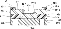
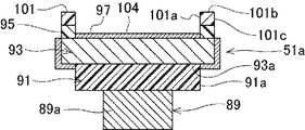
11 and 12 relate to the first embodiment provided with a barrier portion. FIG. 11 is an enlarged cross-sectional view of a main part corresponding to the AA line arrow of FIG. FIG. 12 is an enlarged cross-sectional view of a main part corresponding to the view taken along the line B-B in FIG. The basic configuration will be described with reference to Reference Examples 1 and 2, and the corresponding components will be described using the same reference numerals.
図11、図12では、テール端子部51aについて主に説明する。他のテール端子部53a、55a、57a、59a、61a、79a、81a、83a、85aも同一の構造である。なお、グランドとなる例えばテール端子部85aは、グランドのための構造をさらに備える。
11 and 12, the
本実施例1は、例えば、セミアディティブ法により製造したフレキシャーへの適用例である。 The first embodiment is an application example to a flexure manufactured by a semi-additive method, for example.
テール端子部51aは、障壁部101を備えている。この障壁部101は、リフローしたはんだ材に対する障壁となり、例えばはんだ材の流れ止めを行うものである。障壁部101は、他のテール端子部53a、55a、57a、59a、61a、79a、81a、83a、85aにも同様に設けられ、少なくとも端子部間であるテール端子部51a、53a、55a、57a、59a、61a、79a、81a、83a、85aの各間に備えられた構成となっている。
The
障壁部101を形成するために、本実施例1では、テール端子部51aにおいて端子部ベース絶縁層91の中央部を薄く形成して薄層部103を選択的に備えた。薄層部103は、均一な層厚に形成されている。但し、薄層部103の一部を厚くし、さらに薄くすることもできる。
In order to form the
この薄層部103を含む端子部ベース絶縁層91に倣って端子層93を形成している。障壁部101は、端子層93の中央部周囲を囲む形態で端子面上を凹状とし、はんだ溜まり凹部104を形成している。
A
障壁部101は、図11で示すA−A線断面の方向が図12で示すB−B線断面の方向に対し相対的に短く形成され、平面から見て長方形状の枠を構成している。
The
端子部ベース絶縁層91の中央部は、端子部金属支持層89の島状部89aにより補強されている。
The central portion of the terminal portion
障壁部101は、断面において周回状の内面101a、上面101b、ほぼ周回状の外面101cを備えている。外面101cをほぼ周回状としたのは、図12で示すB−B線断面の一方側、例えば図中左側において、端子部金属支持層89、端子部ベース絶縁層91、端子層93、端子部カバー絶縁層95が図4のように配線部49として連続し、完全な周回状ではないためである。
The
図11で示すA−A線断面では、障壁部101は、テール端子部51a、・・・が隣接配置された方向の両側にテール端子部51aの端子面を挟むように備えられている。但し、障壁部101は、はんだリフロー時にはんだ材の流れを規制できればよく、テール端子部51aの片側に形成され、或いはテール端子部51a、・・・の一つ置きに両側に備える形態にすることもできる。
11, the
障壁部101の下方で端子層93の下面93a側に端子部ベース絶縁層91の外縁部91aが位置し、障壁部101を支持する。金メッキ97は、端子層93の中央部の端子面から障壁部101の内面101a、上面101b、外面101c、及び端子層93の下面93aに渡って形成されている。
The
図12で示すB−B線断面では、障壁部101は、テール端子部51aが隣接配置された方向に交差する両側にテール端子部51aの端子面を挟むように備えられている。端子層93の下面93aに端子部ベース絶縁層91の外縁部91aが位置してこれを支持し、端子部ベース絶縁層91の外縁部91aを端子部金属支持層89の側壁部89bが支持している。
In the cross section taken along line B-B shown in FIG. 12, the
[製造方法]
フレキシャー43の製造方法を、テール端子部51aを中心に説明する。
[Production method]
A method of manufacturing the
(第1工程)
第1工程では、金属支持層47を形成するためのステンレス基材(SST基材)を準備する。
(First step)
In the first step, a stainless steel substrate (SST substrate) for forming the
(第2工程)
第2工程において、ステンレス基材上に感光性ポリイミドを全体的に塗布する。次いで、金属支持層47、端子部金属支持層89となる部分に、露光により端子部ベース絶縁層91を含めてベース絶縁層を形成すると共に、端子部ベース絶縁層91の中央部を薄く形成して薄層部103とする。薄層部103は、端子部ベース絶縁層91のエッチング、レーザー処理によっても形成することができる。
(Second step)
In the second step, the photosensitive polyimide is entirely applied on the stainless steel substrate. Next, a base insulating layer including the terminal portion
(第3工程)
第3工程において、端子部ベース絶縁層91上を含めてベース絶縁層上にレジストを所定パターンで形成して銅メッキにより端子層93を含めて配線層99(図6参照。)を形成し、レジストを剥離する。
(Third step)
In the third step, a resist is formed in a predetermined pattern on the base insulating layer including the terminal portion
(第4工程)
第4工程において、端子層93等に、配線層99上を被覆するように端子部カバー絶縁層95を含めて配線部49のカバー絶縁層を形成する。
(4th process)
In the fourth step, a cover insulating layer of the
ここで、図11のように端子部ベース絶縁層91が端子層93の配線幅より狭い場合、SST基材側から端子部ベース絶縁層91をエッチングする必要があり、本工程の次に行われる。
Here, when the terminal
つまり、本工程の次に、SST基材の部分的なエッチングを行い、ベース絶縁層のエッチングにより図11のような端子部ベース絶縁層91を形成する。
That is, following this step, the SST base material is partially etched, and the terminal insulating
(第5工程)
第5工程において、端子層93に金メッキ97を形成する。
(5th process)
In the fifth step, a
(第6工程)
SST基材をエッチングして金属支持層47と一体に端子部金属支持層89を形成し、フレキシャーの連鎖品を形成する。この場合、エッチングにより他の箇所の所定形状と共に島状部89a及び側壁部89bが形成される。
(Sixth step)
The SST base material is etched to form a terminal
その後、単体のフレキシャー43が切り離される。
Thereafter, the
[はんだ接合]
図11、図12で示すテール端子部51aと基板端子部23aとの接合に示すように、テール端子部51a、53a、55a、57a、59a、61a、79a、81a、83a、85aと、外部端子である回路基板の基板端子部23a、・・・(図4参照。)とが対応して重ねられる。マイクロはんだボールを使用したリフローによりテール端子部51a、・・・、基板端子部23a、・・・間にはんだ材のフィレット87を形成してはんだ接合し、接続信頼性を向上させている。
[Solder bonding]
As shown in the joining of the
特にテール端子部51a、53a、55a、57a、59a、61a、79a、81a、83a、85aが連続して隣接する図11で示すA−A線断面では、障壁部101が、テール端子部51a、53a、55a、57a、59a、61a、79a、81a、83a、85aの隣接方向間に存在する。
In particular, the
しかも、図12で示すB−B線断面でも、テール端子部51a、53a、55a、57a、59a、61a、79a、81a、83a、85aに障壁部101が存在する。
Moreover, the
このため、障壁部101により各テール端子部51a、・・・に、はんだ溜まり凹部104が形成される。
For this reason, the solder reservoir recessed
障壁部101によりはんだ材の流れを規制し、はんだ溜まり凹部104によりはんだ材を溜め、はんだフィレット87を形成する。
The flow of the solder material is regulated by the
[実施例1の効果]
本発明実施例のフレキシャー43は、基板をなす端子部金属支持層89を含む金属性の金属支持層47、金属支持層47の表面に備えられた端子部ベース絶縁層91を含む絶縁性のベース絶縁層と、ベース絶縁層の表面に複数本の配線として配索された端子層93を含む配線層99と、配線を被覆する絶縁性の端子部カバー絶縁層95を含むカバー絶縁層と、複数の配線に備えられ連続的に隣接配置された複数のテール端子部51a、53a、55a、57a、59a、61a、79a、81a、83a、85aとを備え、複数のテール端子部51a、・・・が対応する複数の基板端子部23a、25a、27a、29a、31a、33a、・・・にそれぞれはんだ材によりはんだ接合されるフレキシャー43であって、はんだ材に対する障壁部101をテール端子部51a、・・・に備えた。
[Effect of Example 1]
The
このため、はんだリフロー時に障壁部101及びはんだ溜まり凹部104の働きではんだ材の流れ止めが行なわれ、はんだブリッジの発生を確実に抑制できる。
For this reason, at the time of solder reflow, the flow of the solder material is performed by the action of the
特に、障壁部101の存在により障壁部101の先端縁部と基板端子部23a、・・・との間隔が端子層93の端子表面に比較して狭くなり、はんだ溜まり凹部104にはんだ材を収容しながら障壁部101の縁部と基板端子部23a、・・・との間で表面張力を有効に働かせることができる。
In particular, due to the presence of the
このため、障壁部101での障壁の作用及び障壁部101と基板端子部23a、・・・との間隔での表面張力の作用によりリフローされたはんだ材が障壁部101と基板端子部23a、・・・との間から流れ難くなる。
For this reason, the solder material reflowed by the action of the barrier in the
しかも、端子層93の端子表面と基板端子部23a、・・・との間隔を従来に比較して拡げたはんだ溜まり凹部104にすることもできるため、はんだ溜まり凹部104に十分なはんだ材を確保し、大きさの十分なはんだフィレット87を作ることができる。
In addition, since the distance between the terminal surface of the
なお、障壁部101の形成は、端子部ベース絶縁層91の露光等により形成するだけであり、製造が容易である。端子部ベース絶縁層91の厚みは薄くなるが、局部的であり、影響はない。端子層93は、従来と同様の厚みを確保することができる。
The
[実施例1の変形例1]
図13、図14は、障壁部を備えた実施例1の変形例1を示す。図13は、図8のA−A線矢視に対応する要部拡大断面図である。図14は、図8のB−B線矢視に対応する要部拡大断面図である。なお、基本的な構成については参考例1、2、実施例1を参照し、対応する構成部分は、同符号を用い、実施例1との相違について説明する。重複した説明は、省略する。
[Modification 1 of Example 1]
13 and 14 show a first modification of the first embodiment that includes a barrier portion. FIG. 13 is an enlarged cross-sectional view of a main part corresponding to the line AA in FIG. FIG. 14 is an enlarged cross-sectional view of a main part corresponding to the arrow BB in FIG. Reference examples 1 and 2 and Example 1 are referred to for the basic configuration, and the corresponding components are denoted by the same reference numerals, and differences from Example 1 will be described. A duplicate description is omitted.
本実施例1の変形例1は、例えば、セミアディティブ法により製造したフレキシャーへの適用例である。 Modification 1 of the first embodiment is an application example to a flexure manufactured by a semi-additive method, for example.
本実施例1の変形例1でも、図13、図14で示すテール端子部51aについて主に説明することは上記同様である。
In the first modification of the first embodiment, the
図11、図12の実施例1では、端子部ベース絶縁層91のテール端子部51a、・・・隣接方向での幅が図11のように端子層93の幅よりも小さく形成されているのに対し、図13、図14の本実施例1の変形例1では、端子部ベース絶縁層91の外縁部91aを伸ばし、端子部ベース絶縁層91のテール端子部51a、・・・隣接方向での幅を端子層93の幅よりも大きくした。
11 and 12, the
従って、本実施例1の変形例1では、端子部ベース絶縁層91の外縁部91aにより端子層93の下面93aを十分に支持することができる。
Therefore, in the first modification of the first embodiment, the
また、本実施例1の変形例1でも、障壁部101及びはんだ溜まり凹部104により、上記実施例1と同様な作用効果を得ることができる。
Also in the first modification of the first embodiment, the same effect as that of the first embodiment can be obtained by the
[実施例1の変形例2]
図15、図16は、障壁部を備えた実施例1の変形例2を示す。図15は、図8のA−A線矢視に対応する要部拡大断面図である。図16は、図8のB−B線矢視に対応する要部拡大断面図である。なお、基本的な構成については参考例1、2、実施例1を参照し、対応する構成部分は、同符号を用い、実施例1との相違について説明する。重複した説明は、省略する。
[Modification 2 of Embodiment 1]
15 and 16 show a second modification of the first embodiment provided with a barrier portion. FIG. 15 is an enlarged cross-sectional view of a main part corresponding to the line AA in FIG. FIG. 16 is an enlarged cross-sectional view of a main part corresponding to the arrow BB in FIG. Reference examples 1 and 2 and Example 1 are referred to for the basic configuration, and the corresponding components are denoted by the same reference numerals, and differences from Example 1 will be described. A duplicate description is omitted.
本実施例1の変形例2は、例えば、セミアディティブ法により製造したフレキシャーへの適用例である。 Modification 2 of the first embodiment is an application example to a flexure manufactured by a semi-additive method, for example.
本実施例1の変形例2でも、図15、図16で示すテール端子部51aについて主に説明することは上記同様である。
In the second modification of the first embodiment, the
図11、図12の実施例1では、端子部ベース絶縁層91及び島状部89aのテール端子部51a、・・・隣接方向での幅が図11のように端子層93の幅よりも小さく形成されているのに対し、図15、図16の本実施例1の変形例2では、端子部ベース絶縁層91の外縁部91a及び島状部89aを伸ばし、端子部ベース絶縁層91のテール端子部51a、・・・隣接方向での幅を端子層93の幅よりも大きくした。
11 and 12, the terminal
従って、本実施例1の変形例2では、端子部ベース絶縁層91の外縁部91a及び端子部金属支持層89の島状部89aにより端子層93の下面93aを十分に支持することができる。
Therefore, in the second modification of the first embodiment, the
また、本実施例1の変形例2でも、障壁部101及びはんだ溜まり凹部104により、上記実施例1と同様な作用効果を得ることができる。
In the second modification of the first embodiment, the same effect as that of the first embodiment can be obtained by the
[実施例1の変形例3]
図17、図18は、障壁部を備えた実施例1の変形例3を示す。図17は、図8のA−A線矢視に対応する要部拡大断面図である。図18は、図8のB−B線矢視に対応する要部拡大断面図である。なお、基本的な構成については参考例1、2、実施例1を参照し、対応する構成部分は、同符号を用い、実施例1との相違について説明する。重複した説明は、省略する。
[
17 and 18 show a third modification of the first embodiment provided with a barrier portion. FIG. 17 is an enlarged cross-sectional view of a main part corresponding to the line AA in FIG. 18 is an enlarged cross-sectional view of a main part corresponding to the view taken along line B-B in FIG. 8. Reference examples 1 and 2 and Example 1 are referred to for the basic configuration, and the corresponding components are denoted by the same reference numerals, and differences from Example 1 will be described. A duplicate description is omitted.
本実施例1の変形例3は、例えば、セミアディティブ法により製造したフレキシャーへの適用例である。
本実施例1の変形例3でも、図17、図18で示すテール端子部51aについて主に説明することは上記同様である。
Also in the third modification of the first embodiment, the
図11、図12の実施例1では、端子部金属支持層89の島状部89aを有しているのに対し、図17、図18の本実施例1の変形例3では、端子部金属支持層89の島状部89aを省いた。
11 and 12 includes the island-shaped
従って、本実施例1の変形例3では、テール端子部51a、・・・の可撓性を向上させ、軽量化を図ることもできる。
Therefore, in the third modification of the first embodiment, the flexibility of the
また、本実施例1の変形例3でも、障壁部101及びはんだ溜まり凹部104により、上記実施例1と同様な作用効果を得ることができる。
In the third modification of the first embodiment, the same effect as that of the first embodiment can be obtained by the
[実施例1の変形例4]
図19、図20は、障壁部を備えた実施例1の変形例4を示す。図19は、図8のA−A線矢視に対応する要部拡大断面図である。図20は、図8のB−B線矢視に対応する要部拡大断面図である。なお、基本的な構成については参考例1、2、実施例1を参照し、対応する構成部分は、同符号を用い、実施例1との相違について説明する。重複した説明は、省略する。
[Modification 4 of Example 1]
19 and 20 show a fourth modification of the first embodiment provided with a barrier portion. FIG. 19 is an enlarged cross-sectional view of a main part corresponding to the line AA in FIG. 20 is an enlarged cross-sectional view of a main part corresponding to the view taken along the line B-B in FIG. 8. Reference examples 1 and 2 and Example 1 are referred to for the basic configuration, and the corresponding components are denoted by the same reference numerals, and differences from Example 1 will be described. A duplicate description is omitted.
本実施例1の変形例4は、例えば、サブトラクティブ法により製造したフレキシャーへの適用例である。 Modification 4 of the first embodiment is an application example to a flexure manufactured by a subtractive method, for example.
本実施例1の変形例4でも、図19、図20で示すテール端子部51aについて主に説明することは上記同様である。
In the fourth modification of the first embodiment, the
図11、図12の実施例1では、端子部ベース絶縁層91の中央部を薄く形成して薄層部103とし、障壁部101及びはんだ溜まり凹部104を設けたのに対し、図19、図20の本実施例1の変形例4では、端子部ベース絶縁層91は薄く形成せず、端子層93の中央部を薄く形成して薄層部105を選択的に形成して備え、障壁部101及びはんだ溜まり凹部104を設けた。
11 and 12, the central portion of the terminal
図19で示すA−A線断面での端子層93の中央部の幅は、図20で示すB−B線断面での端子層93の中央部の幅よりも狭く平面から見て長方形の枠となる障壁部101を形成した。障壁部101の内側は、はんだ溜まり凹部104となる。
The width of the central portion of the
端子層93の中央部の薄層部105は、銅のパーシャルエッチングで行うことができる。
The
従って、本実施例1の変形例4でも、障壁部101及びはんだ溜まり凹部104により、上記実施例1と同様な作用効果を得ることができる。
Therefore, also in the fourth modification of the first embodiment, the same effect as that of the first embodiment can be obtained by the
また、本実施例1の変形例4では、障壁部101の形成は、端子層93のパーシャルエッチングによる薄層部105の形成によるだけであり、製造が容易である。
In the fourth modification of the first embodiment, the formation of the
端子層93は、従来と同様な厚みの端子部ベース絶縁層91により支持させることができる。
The
[実施例1の変形例5]
図21、図22は、障壁部を備えた実施例1の変形例5を示す。図21は、図8のA−A線矢視に対応する要部拡大断面図である。図22は、図8のB−B線矢視に対応する要部拡大断面図である。なお、基本的な構成については参考例1、2、実施例1を参照し、対応する構成部分は、同符号を用い、実施例1との相違について説明する。
[
21 and 22 show a fifth modification example of the first embodiment including a barrier portion. FIG. 21 is an enlarged cross-sectional view of a main part corresponding to the line AA in FIG. 22 is an enlarged cross-sectional view of a main part corresponding to the view taken along line B-B in FIG. 8. Reference examples 1 and 2 and Example 1 are referred to for the basic configuration, and the corresponding components are denoted by the same reference numerals, and differences from Example 1 will be described.
本実施例1の変形例5は、例えば、セミアディティブ法により製造したフレキシャーへの適用例である。 The fifth modification of the first embodiment is an application example to a flexure manufactured by a semi-additive method, for example.
本実施例1の変形例5では、図21、図22で示すグランド端子であるテール端子部85aについての適用を説明するが、他のテール端子部51a、53a、55a、57a、59a、61a、79a、81a、83aは、前記テール端子部51aと同様に構成されている。
In the fifth modification of the first embodiment, the application to the
図11、図12の実施例1では、端子部ベース絶縁層91の中央部を薄く形成して薄層部103とし、障壁部101及びはんだ溜まり凹部104を設けたのに対し、図21、図22の変形例5では、グランド端子としてのテール端子部85aの端子部ベース絶縁層91は薄く形成せず、孔として接地部のビアホール(Via hole)107a、107bを選択的に形成して備え、障壁部101及びはんだ溜まり凹部104を設けた。
11 and 12, the central portion of the terminal
図21で示すA−A線断面では、図22で示すB−B線断面で示されるビアホール107a、107bの一方のビアホール107aを示し、ビアホール107a内に渡って端子層93が形成されている。ビアホール107a内で端子層93は、端子部金属支持層89の島状部89aに接地している。端子層93の中央部に、はんだ溜まり凹部104が段付き状に形成され、その両側に障壁部101を形成している。障壁部101は、A−A線断面で幅が拡大されている。
The cross section taken along line AA shown in FIG. 21 shows one via
図21で示すA−A線断面では現れないビアホール107bについても、同様の断面構成となっている。
The via
図22で示すB−B線断面では、端子部ベース絶縁層91のビアホール107a、107bが中央の低壁91bを挟んで一対備えられ、端子層93の中央部周囲を薄く形成している。端子層93の中央に凸部93bが形成され、凸部93bを挟んではんだ溜まり凹部104を段付き状に形成している。障壁部101の内面101aも段付き状となっている。
22, a pair of via
ビアホール107a、107bは、端子部ベース絶縁層91の露光、エッチング、レーザー処理等により形成することができる。セミアディティブ法の工程では、フォトマスクを使用したベース絶縁層形成と同時に、ビアホール107a、107bを形成することもできる。他の例のセミアディティブ法により製造したフレキシャーのビアホールについても同様である。
The via holes 107a and 107b can be formed by exposing the terminal
端子層93の薄層部105は、銅のパーシャルエッチングで行うことができる。
The
従って、本実施例1の変形例5でも、障壁部101及びはんだ溜まり凹部104により、上記実施例1と同様な作用効果を得ることができる。
Therefore, also in the fifth modification of the first embodiment, the same effect as that of the first embodiment can be obtained by the
また本実施例1の変形例5では、はんだ溜まり凹部104を段付き状に深くすることができ、障壁部101の機能を増幅させることができる。
In the fifth modification of the first embodiment, the
[実施例1の変形例6]
図23、図24は、障壁部を備えた実施例1の変形例6を示す。図23は、図8のA−A線矢視に対応する要部拡大断面図である。図24は、図8のB−B線矢視に対応する要の部拡大断面図である。なお、基本的な構成については参考例1、2、実施例1を参照し、対応する構成部分は、同符号を用い、実施例1との相違について説明する。
[Modification 6 of Example 1]
23 and 24 show a sixth modified example of the first embodiment provided with a barrier portion. FIG. 23 is an enlarged cross-sectional view of the main part corresponding to the arrow AA in FIG. 24 is an essential part enlarged cross-sectional view corresponding to the view taken along line B-B in FIG. 8. Reference examples 1 and 2 and Example 1 are referred to for the basic configuration, and the corresponding components are denoted by the same reference numerals, and differences from Example 1 will be described.
本実施例1の変形例6は、例えば、セミアディティブ法により製造したフレキシャーへの適用例である。 The sixth modification of the first embodiment is an application example to a flexure manufactured by a semi-additive method, for example.
本実施例1の変形例6では、図23、図24で示すグランド端子であるテール端子部85aについての適用を説明することは変形例5と同様である。
In the sixth modification of the first embodiment, the application of the
図11、図12の実施例1では、端子部ベース絶縁層91の中央部を薄く形成して薄層部103とし、障壁部101及びはんだ溜まり凹部104を設けたのに対し、図23、図24の変形例6では、グランド端子としてのテール端子部85aの端子部ベース絶縁層91は薄く形成せず、孔として接地部のビアホール107を形成することで障壁部101及びはんだ溜まり凹部104を設けた。
11 and 12, the central portion of the terminal
本変形例6のビアホール107は、変形例5の一対のビアホール107a、107bに対して図24のB−B線断面方向の長穴状の形態とした。
The via
図23で示すA−A線断面では、ビアホール107内に渡って端子層93が形成され、中央にはんだ溜まり凹部104が形成され、幅が拡大された障壁部101を形成している。
In the cross section taken along line AA shown in FIG. 23, a
図24で示すB−B線断面では、ビアホール107の幅が図23で示すA−A線断面よりも大きく形成され、且つ端子層93の中央部両側を薄く形成して薄層部105としている。はんだ溜まり凹部104は、端子層93の中央から両側に段付き状に形成されている。
24, the width of the via
ビアホール107は、レーザー処理等により加工することができる。端子層93の薄層部105は、銅のパーシャルエッチングで行うことができる。
The via
従って、本実施例1の変形例6でも、障壁部101及びはんだ溜まり凹部104により、上記実施例1と同様な作用効果を得ることができる。
Therefore, also in the sixth modification of the first embodiment, the same effect as that of the first embodiment can be obtained by the
また本実施例1の変形例6でも、同変形例5と同様な作用効果を得ることができる。 In the sixth modification of the first embodiment, the same operational effects as in the fifth modification can be obtained.
[実施例1の変形例7]
図25、図26は、障壁部を備えた実施例1の変形例7を示す。図25は、図8のA−A線矢視に対応する要部拡大断面図である。図26は、図8のB−B線矢視に対応する要部拡大断面図である。なお、基本的な構成については参考例1、2、実施例1、変形例6を参照し、対応する構成部分は、同符号を用い、実施例1、変形例6との相違について説明する。重複した説明は、省略する。
[
25 and 26 show a seventh modification of the first embodiment provided with a barrier portion. FIG. 25 is an enlarged cross-sectional view of a main part corresponding to the arrow AA in FIG. FIG. 26 is an enlarged cross-sectional view of a main part corresponding to the view taken along line B-B in FIG. 8. Reference examples 1 and 2, Example 1, and Modification 6 are referred to for the basic configuration, and the corresponding components are denoted by the same reference numerals, and differences from Example 1 and Modification 6 will be described. A duplicate description is omitted.
本実施例1の変形例7は、例えば、セミアディティブ法により製造したフレキシャーへの適用例である。
本実施例1の変形例7でも、図25、図26で示すグランド端子であるテール端子部85aについて主に説明することは上記同様である。
In the seventh modification of the first embodiment, the
図23、図24の実施例1の変形例6では、図24のように端子層93の中央部両側を銅のパーシャルエッチングにより薄く形成して薄層部105としたのに対し、図25、図26の本実施例1の変形例7では、変形例6の薄層部105を設けず、端子層93の中央部両側を中央部と略同一厚みとした。
In the sixth modification of the first embodiment shown in FIGS. 23 and 24, both sides of the central portion of the
従って、本実施例1の変形例7では、パーシャルエッチングを省略することができる。 Therefore, in the seventh modification of the first embodiment, partial etching can be omitted.
また、本実施例1の変形例7では、端子部ベース絶縁層91の外縁部91a及び端子部金属支持層89の島状部89aにより端子層93の下面93aを十分に支持することができる。
Further, in the seventh modification of the first embodiment, the
また、本実施例1の変形例7でも、障壁部101及びはんだ溜まり凹部104により、上記実施例1と同様な作用効果を得ることができる。
In the seventh modification of the first embodiment, the same effect as that of the first embodiment can be obtained by the
[実施例1の変形例8]
図27、図28は、障壁部を備えた実施例1の変形例8を示す。図27は、図8のA−A線矢視に対応する要部拡大断面図である。図28は、図8のB−B線矢視に対応する要部拡大断面図である。なお、基本的な構成については参考例1、2、実施例1、変形例6を参照し、対応する構成部分は、同符号を用い、実施例1、変形例6との相違について説明する。重複した説明は、省略する。
[Modification 8 of Example 1]
27 and 28 show a modification 8 of the embodiment 1 including a barrier portion. FIG. 27 is an enlarged cross-sectional view of a main part corresponding to the line AA in FIG. FIG. 28 is an enlarged cross-sectional view of a main part corresponding to the arrow BB in FIG. Reference examples 1 and 2, Example 1, and Modification 6 are referred to for the basic configuration, and the corresponding components are denoted by the same reference numerals, and differences from Example 1 and Modification 6 will be described. A duplicate description is omitted.
本実施例1の変形例8は、例えば、セミアディティブ法により製造したフレキシャーへの適用例である。 The eighth modification of the first embodiment is an application example to a flexure manufactured by a semi-additive method, for example.
本実施例1の変形例8でも、図27、図28で示すグランド端子であるテール端子部85aについて主に説明することは上記同様である。
In the modification 8 of the first embodiment, the
図23、図24の実施例1の変形例6では、端子部金属支持層89の島状部89aを有しているのに対し、図27、図28の本実施例1の変形例8では、端子部金属支持層89の島状部89aを省いた。
In the sixth modification of the first embodiment shown in FIGS. 23 and 24, the island-shaped
従って、本実施例1の変形例8では、テール端子部85aの可撓性を向上させ、軽量化を図ることもできる。
Therefore, in the eighth modification of the first embodiment, the flexibility of the
また、本実施例1の変形例8でも、障壁部101及びはんだ溜まり凹部104により、上記実施例1と同様な作用効果を得ることができる。
In the eighth modification of the first embodiment, the same effect as that of the first embodiment can be obtained by the
[実施例1の変形例9]
図29、図30は、障壁部を備えた実施例1の変形例9を示す。図29は、図8のA−A線矢視に対応する要部拡大断面図である。図30は、図8のB−B線矢視に対応する要部拡大断面図である。なお、基本的な構成については参考例1、2、実施例1を参照し、対応する構成部分は、同符号を用い、実施例1との相違について説明する。
[
29 and 30 show a ninth modification of the first embodiment provided with a barrier portion. FIG. 29 is an enlarged cross-sectional view of a main part corresponding to the line AA in FIG. 30 is an enlarged cross-sectional view of a main part corresponding to the view taken along the line B-B in FIG. 8. Reference examples 1 and 2 and Example 1 are referred to for the basic configuration, and the corresponding components are denoted by the same reference numerals, and differences from Example 1 will be described.
本実施例1の変形例9は、例えば、サブトラクティブ法により製造したフレキシャーへの適用例である。
本実施例1の変形例9では、図29、図30で示すグランド端子であるテール端子部85aについての適用を説明することは上記同様である。
In the ninth modification of the first embodiment, the application of the
図11、図12の実施例1では、端子部ベース絶縁層91の中央部を薄く形成して薄層部103とし、障壁部101及びはんだ溜まり凹部104を設けたのに対し、図29、図30の本変形例9では、テール端子部85aの端子部ベース絶縁層91は薄く形成せず、孔として接地部のビアホール(107a、108a)、(107b、108b)を選択的に形成して備え、このビアホール(107a、108a)、(107b、108b)にニッケルメッキのグランド109a、109bを形成して障壁部101及びはんだ溜まり凹部104を設けた。
11 and 12, the central portion of the terminal
つまり、障壁部101を、ベース絶縁層の端子部ベース絶縁層91と配線層99の端子層93とに渡って形成され金属支持層である端子部金属支持層89に接地されたグランド109a、109bに設けている。
That is, the
図29で示すA−A線断面では、一方のグランド109aを示し、ビアホール(107a、108a)にグランド109aが形成され、グランド109aは、端子部金属支持層89の島状部89aに接地している。グランド109aの中央にはんだ溜まり凹部104が形成され、周囲に障壁部101を構成している。
29 shows one
図29で示すA−A線断面では現れないビアホール(107b、108b)についても同様である。 The same applies to the via holes (107b and 108b) that do not appear in the cross section along the line AA shown in FIG.
図30で示すB−B線断面では、ビアホール(107a、108a)、(107b、108b)が中央の低壁91bを挟んで一対備えられ、ビアホール(107a、108a)、(107b、108b)にグランド109a、109bが各別に形成されている。
In the cross section taken along the line B-B shown in FIG. 30, a pair of via holes (107a, 108a), (107b, 108b) are provided with a central
ビアホール(107a、108a)、(107b、108b)は、端子層93及び端子部ベース絶縁層91のレーザー処理等による加工で形成できる。また、端子層93の銅をエッチングにより除去してから端子部ベース絶縁層91をレーザー処理やエッチングして形成することもできる。グランド109a、109bは、フォトマスクでマスキングして形成することができる。
The via holes (107a, 108a) and (107b, 108b) can be formed by processing the
従って、本実施例1の変形例9でも、障壁部101及びはんだ溜まり凹部104により、上記実施例1と同様な作用効果を得ることができる。
Therefore, also in the ninth modification of the first embodiment, the same effect as the first embodiment can be obtained by the
また本実施例1の変形例9では、障壁部101及びはんだ溜まり凹部104をグランド109a、109bのニッケルメッキを利用して形成することができ、工程の増加がなく、容易に製造することができる。
Further, in the ninth modification of the first embodiment, the
[実施例1の変形例10]
図31、図32は、障壁部を備えた実施例1の変形例10を示す。図31は、図8のA−A線矢視に対応する要部拡大断面図である。図32は、図8のB−B線矢視に対応する要部拡大断面図である。なお、基本的な構成については参考例1、2、実施例1を参照し、対応する構成部分は、同符号を用い、実施例1、変形例9との相違について説明する。
[Modification 10 of Example 1]
31 and 32 show a tenth modification of the first embodiment provided with a barrier portion. FIG. 31 is an enlarged cross-sectional view of a main part corresponding to the line AA in FIG. FIG. 32 is an enlarged cross-sectional view of a main part corresponding to the arrow BB in FIG. Reference examples 1 and 2 and Example 1 are referred to for the basic configuration, and the corresponding components are denoted by the same reference numerals, and differences from Example 1 and
本実施例1の変形例10は、例えば、サブトラクティブ法により製造したフレキシャーへの適用例である。 The tenth modification of the first embodiment is an application example to a flexure manufactured by a subtractive method, for example.
本実施例1の変形例10では、図31、図32で示すグランド端子であるテール端子部85aについての適用を説明することは上記同様である。
In the tenth modification of the first embodiment, the application of the
図11、図12の実施例1では、端子部ベース絶縁層91の中央部を薄く形成して薄層部103とし、障壁部101及びはんだ溜まり凹部104を設けたのに対し、図31、図32の変形例10では、テール端子部85aの端子部ベース絶縁層91は薄く形成せず、孔として接地部のビアホール107、108を形成し、このビアホール107、108にニッケルメッキのグランド109を形成して障壁部101及びはんだ溜まり凹部104を設けた。
11 and 12, the central portion of the terminal portion
つまり、障壁部101を、ベース絶縁層の端子部ベース絶縁層91と配線層99の端子層93とに渡って形成されたグランド109に設けている。
That is, the
本変形例10のビアホール107、108は、単一の長穴として形成され、変形例9の一対のビアホール(107a、108a)、(107b、108b)に対し、単一のビアホール107、108であることに相違がある。その他は、変形例9と同様である。
The via holes 107 and 108 of the present modification 10 are formed as a single elongated hole, and are a single via
従って、本実施例1の変形例10でも、障壁部101及びはんだ溜まり凹部104により、上記実施例1、変形例9と同様な作用効果を得ることができる。
Therefore, also in the tenth modification of the first embodiment, the same effect as the first embodiment and the ninth modification can be obtained by the
[実施例1の変形例11]
図33、図34は、障壁部を備えた実施例1の変形例11を示す。図33は、図8のA−A線矢視に対応する要部拡大断面図である。図34は、図8のB−B線矢視に対応する要部拡大断面図である。なお、基本的な構成については参考例1、2、実施例1を参照し、対応する構成部分は、同符号を用いて説明する。
[
33 and 34 show a
本実施例1の変形例11は、例えば、セミアディティブ法により製造したフレキシャーへの適用例である。
本実施例1の変形例11では、図33、図34で示すグランド端子であるテール端子部85aについての適用を説明することは上記同様である。
In the eleventh modification of the first embodiment, the application of the
図11、図12の実施例1では、端子部ベース絶縁層91の中央部を薄く形成して薄層部103とし、障壁部101及びはんだ溜まり凹部104を設けたのに対し、図32、図33の本実施例1の変形例11では、テール端子部85aの端子部ベース絶縁層91は薄く形成せず、端子部ベース絶縁層91に孔である接地部のビアホール107を形成し、このビアホール107内に渡って端子層93を形成し障壁部101及びはんだ溜まり凹部104を設けた。ビアホール107は、単一の穴として形成されている。
11 and 12, the central portion of the terminal portion
図33で示すA−A線断面及び図34で示すB−B線断面のように、ビアホール107に形成された端子層93は、端子部金属支持層89の島状部89aに接地している。端子層93の中央にビアホール108が形成され、はんだ溜まり凹部104が段付き状に形成され、周囲に障壁部101を形成している。金メッキ97は、端子層93のビアホール108に渡って形成され、端子層93及び金メッキ97は、端子部金属支持層89の島状部89aに接地している。
The
ビアホール107は、端子部ベース絶縁層91をレーザー処理やエッチングにより加工することで形成できる。ビアホール108は、端子層93の銅をエッチングにより除去し、或いはレーザー処理により加工することで形成できる。
The via
従って、本実施例1の変形例11でも、障壁部101及びはんだ溜まり凹部104により、上記実施例1と同様な作用効果を得ることができる。
Therefore, also in the eleventh modification of the first embodiment, the same effect as the first embodiment can be obtained by the
また本実施例1の変形例11では、上記各実施例に比較してより深いはんだ溜まり凹部104を形成することができ、障壁部101の機能をより増幅させることができる。
In the eleventh modification of the first embodiment, the deeper
図35、図36は、実施例2を示す。図35は、図8のA−A線矢視に対応する要部拡大断面図である。図36は、図8のB−B線矢視に対応する要部拡大断面図である。なお、基本的な構成については参考例1、2、実施例1を参照し、対応する構成部分は、同符号を用い、実施例1との相違について説明する。 35 and 36 show the second embodiment. FIG. 35 is an enlarged cross-sectional view of a main part corresponding to the line AA in FIG. FIG. 36 is an enlarged cross-sectional view of a main part corresponding to the view taken along line B-B in FIG. 8. Reference examples 1 and 2 and Example 1 are referred to for the basic configuration, and the corresponding components are denoted by the same reference numerals, and differences from Example 1 will be described.
本実施例2でも、図35、図36で示すテール端子部51aについて主に説明することは実施例1と同様である。
In the second embodiment, the
図11、図12の実施例1では、端子部ベース絶縁層91の中央部を薄く形成して薄層部103とし、障壁部101及びはんだ溜まり凹部104を設けたのに対し、図35、図36の実施例2では、端子層93の中央部周囲を凸状に形成して障壁部101及びはんだ溜まり凹部104を設けた。
11 and 12, the central portion of the terminal portion
図35、図36のように、凸部としての障壁部101は、端子層93上に中央部を囲むように凸状に形成されている。端子層93上には、障壁部101で囲まれたはんだ溜まり凹部104が形成される。金メッキ97は、障壁部101をも覆うように形成されている。
As shown in FIGS. 35 and 36, the
障壁部101は、実施例1の変形例9、10のように、ニッケルのグランドをフォトマスクでマスキングして形成するときに同時に形成することができる。
The
本実施例の障壁部101の場合は、グランド端子とするテール端子部85aのように、端子部ベース絶縁層91や端子層93に孔がないのでニッケルメッキのグランドと同時形成したとき端子層93上で嵩高となる。
In the case of the
従って、本実施例2でも、障壁部101及びはんだ溜まり凹部104により、上記実施例1と同様な作用効果を得ることができる。
Therefore, also in the second embodiment, the same effect as the first embodiment can be obtained by the
また本実施例2では、端子層93上に突出する障壁部101により基板端子部23a、・・・との間隔をより狭くすることができ、障壁部101及びはんだ溜まり凹部104の機能をより向上させることができる。
In the second embodiment, the distance between the
障壁部101は、ニッケルメッキのグランドと同時形成することができ、容易に製造することができる。
The
[実施例2の変形例1]
図37、図38は、障壁部を備えた実施例2の変形例1を示す。図37は、図8のA−A線矢視に対応する要部拡大断面図である。図38は、図8のB−B線矢視に対応する要部拡大断面図である。なお、基本的な構成については参考例1、2、実施例1を参照し、対応する構成部分は、同符号を用い、実施例1との相違について説明する。
[Modification 1 of Embodiment 2]
37 and 38 show a first modification of the second embodiment that includes a barrier portion. FIG. 37 is an enlarged cross-sectional view of a main part corresponding to the line AA in FIG. 38 is an enlarged cross-sectional view of a main part corresponding to the view taken along the line B-B in FIG. 8. Reference examples 1 and 2 and Example 1 are referred to for the basic configuration, and the corresponding components are denoted by the same reference numerals, and differences from Example 1 will be described.
本実施例2の変形例1でも、図37、図38で示すテール端子部51aについて主に説明することは上記同様である。
Also in the first modification of the second embodiment, the
図11、図12の実施例1では、端子部ベース絶縁層91の中央部を薄く形成して薄層部103とし、障壁部101及びはんだ溜まり凹部104を設けたのに対し、図37、図38の実施例2の変形例1では、端子部カバー絶縁層95に障壁部101を一体に形成し、はんだ溜まり凹部104を設けた。
11 and 12, the central portion of the terminal portion
図37、図38のように、障壁部101は、端子層93の中央部の端子面を囲むように形成されている。
As shown in FIGS. 37 and 38, the
障壁部101は、端子層93において端子部カバー絶縁層95に同じ絶縁材で一体に突出形成されている。
In the
この障壁部101は、端子部カバー絶縁層95の部分で障壁部101を含む高さに絶縁材を塗り、露光やエッチング、レーザー処理等の加工で端子層93を露出させることで形成することができる。
The
従って、本実施例2の変形例1でも、障壁部101及びはんだ溜まり凹部104により、上記実施例1と同様な作用効果を得ることができる。
Therefore, also in the first modification of the second embodiment, the same effect as the first embodiment can be obtained by the
また本実施例2の変形例1では、障壁部101及びはんだ溜まり凹部104を、端子部カバー絶縁層95のエッチング等により形成することができる。
In the first modification of the second embodiment, the
[実施例2の変形例2]
図39、図40は、障壁部を備えた実施例2の変形例2係り、図39は、図8のA−A線矢視に対応する要部拡大断面図である。図40は、図8のB−B線矢視に対応する要部拡大断面図である。なお、基本的な構成については参考例1、2、実施例1を参照し、対応する構成部分は、同符号を用い、実施例1との相違について説明する。
[Modification 2 of Embodiment 2]
39 and 40 relate to the second modification of the second embodiment including the barrier portion, and FIG. 39 is an enlarged cross-sectional view of the main part corresponding to the arrow AA in FIG. 8. 40 is an enlarged cross-sectional view of a main part corresponding to the view taken along the line B-B in FIG. 8. Reference examples 1 and 2 and Example 1 are referred to for the basic configuration, and the corresponding components are denoted by the same reference numerals, and differences from Example 1 will be described.
本実施例2の変形例2でも、図39、図40で示すテール端子部51aについて主に説明することは上記同様である。
In the second modification of the second embodiment, the
図11、図12の実施例1では、端子部ベース絶縁層91の中央部を薄く形成して薄層部103とし、障壁部101及びはんだ溜まり凹部104を設けたのに対し、図39、図40の実施例2の変形例2では、実施例2の変形例1同様に端子部カバー絶縁層95により障壁部101及びはんだ溜まり凹部104を設けた。
11 and 12, the central portion of the terminal
本実施例2の変形例2の障壁部101は、二層に形成され、実施例2の変形例1が単一層であることに対して相違がある。その他は、実施例2の変形例2と同様である。
The
二層の障壁部101は、端子部カバー絶縁層95に対応した部分で絶縁層を重ねて形成し、露光や、エッチング、レーザー処理等の加工で端子層93を露出させることで形成することができる。
The two-
従って、本実施例2の変形例2でも、障壁部101及びはんだ溜まり凹部104により、上記実施例1と同様な作用効果を得ることができる。
Accordingly, also in the second modification of the second embodiment, the same effect as that of the first embodiment can be obtained by the
また本実施例2の変形例2では、障壁部101を構成する絶縁層を端子部カバー絶縁層95にのみ配置することができる。
In the second modification of the second embodiment, the insulating layer constituting the
[実施例2の変形例3]
図41、図42は、障壁部を備えた実施例2の変形例3係り、図41は、図8のA−A線矢視に対応する要部拡大断面図である。図42は、図8のB−B線矢視に対応する要部拡大断面図である。なお、基本的な構成については参考例1、2、実施例1、2を参照し、対応する構成部分は、同符号を用い、実施例1との相違について説明する。
[
41 and 42 relate to the third modification of the second embodiment provided with the barrier portion, and FIG. 41 is an enlarged cross-sectional view of the main part corresponding to the arrow AA in FIG. 42 is an enlarged cross-sectional view of a main part corresponding to the view taken along the line B-B in FIG. 8. Reference examples 1 and 2 and Examples 1 and 2 are referred to for the basic configuration, and the corresponding components are denoted by the same reference numerals, and differences from Example 1 will be described.
本実施例2の変形例3でも、図41、図42で示すテール端子部51aについて主に説明することは上記同様である。
Also in the third modification of the second embodiment, the
図11、図12の実施例1では、端子部ベース絶縁層91の中央部を薄く形成することに基づいて障壁部101及びはんだ溜まり凹部104を設けたのに対し、図41、図42の実施例2の変形例3では、端子部金属支持層89により障壁部101及びはんだ溜まり凹部104を設けた。
11 and 12, the
図41で示すA−A線断面では、端子部金属支持層89の幅が大きく、両側を薄く形成して折り曲げにより立ち上げ、障壁部101及びはんだ溜まり凹部104を形成した。障壁部101の高さは、端子層93の側部中間に達する程度であり、端子層93の側部に対し離間している。凹部104は、図42で示すB−B線断面の方向で両側が開放形態となっている。なお、障壁部101をB−B線断面の方向で両側に伸ばし、側壁部89bに近接させることもできる。
In the cross section taken along line AA shown in FIG. 41, the width of the terminal portion
図42で示すB−B線断面は、参考例2の図10と異なるところはない。 The cross section taken along line B-B shown in FIG. 42 is not different from that of FIG.
従って、本実施例2の変形例3でも、障壁部101及びはんだ溜まり凹部104により、上記実施例1と同様な作用効果を得ることができる。
Therefore, also in the third modification of the second embodiment, the same effect as that of the first embodiment can be obtained by the
また本実施例2の変形例3では、障壁部101を端子部金属支持層89の折り曲げにより形成し、テール端子部51a、・・・の剛性を向上させることができる。
Moreover, in the
図43、図44は、実施例3を示す。図43は、図8のA−A線矢視に対応する要部拡大断面図である。図44は、図8のB−B線矢視に対応する要部拡大断面図である。なお、基本的な構成については参考例1、2、実施例1を参照し、対応する構成部分は、同符号を用い、実施例1との相違について説明する。 43 and 44 show a third embodiment. 43 is an enlarged cross-sectional view of a main part corresponding to the line AA in FIG. 44 is an enlarged cross-sectional view of a main part corresponding to the view taken along the line B-B in FIG. 8. Reference examples 1 and 2 and Example 1 are referred to for the basic configuration, and the corresponding components are denoted by the same reference numerals, and differences from Example 1 will be described.
本実施例3は、デュアルレイヤー配線のフレキシャーへの適用例である。なお、デュアルレイヤー配線は、スペース的な理由或いは電気的な特性向上のために採用される。 The third embodiment is an application example of a dual layer wiring to a flexure. The dual layer wiring is employed for space reasons or for improving electrical characteristics.
本実施例3でも、図43、図44で示すテール端子部51aについて主に説明することは上記同様である。
Also in the third embodiment, the
図11、図12の実施例1では、端子部ベース絶縁層91の中央部を薄く形成して薄層部103とし、障壁部101及びはんだ溜まり凹部104を設けたのに対し、図43、図44の実施例3では、デュアルレイヤー配線に対し端子部ベース絶縁層91の中央部を薄く形成して薄層部103とし、中間絶縁層111に孔111aを形成して障壁部101及びはんだ溜まり凹部104を設けた。
11 and 12, the central portion of the terminal
図43で示すA−A線断面、図44で示すB−B線断面のように、テール端子部51aは、端子部金属支持層89の表面に備えられた端子部ベース絶縁層91と、端子部ベース絶縁層91の表面に形成された端子層93と、端子部カバー絶縁層95と、端子層93を覆う金メッキ97と、中間絶縁層111とからなっている。中間絶縁層111は、配線部の中間絶縁層に含まれる。金メッキ97は、下地にニッケルメッキを施す場合もある。端子層93は、ボトム銅層113aとトップ銅層113bとからなっている。
As shown in the AA line cross section shown in FIG. 43 and the BB line cross section shown in FIG. 44, the
図43で示すA−A線断面では、端子部ベース絶縁層91の薄層部103上に端子層93が形成され、トップ銅層113bの中央部を障壁部101が囲んではんだ溜まり凹部104を形成している。
43, the
つまり、端子部ベース絶縁層91の薄層部103に倣って端子層93が形成されている。トップ銅層113bは、中間絶縁層111の孔111a内に渡って形成され、ボトム銅層113aに接続されている。障壁部101は、トップ銅層113bの中央部のはんだ溜まり凹部104周囲を囲む形態で形成されている。
That is, the
図44で示すB−B線断面では、はんだ溜まり凹部104が、トップ銅層113bの中央部から両側に段付き状となっている。
In the cross section taken along line B-B shown in FIG. 44, the
図43、図44のように、障壁部101は、中間絶縁層111で支持されている。障壁部101の下方でトップ銅層113bの下面113baに中間絶縁層111の外縁部111cが位置する。中間絶縁層111の外縁部111cの下側に位置するボトム銅層113aの下面93aに端子部ベース絶縁層91の外縁部91aが位置する。端子部ベース絶縁層91の外縁部91aを端子部金属支持層89の側壁部89bが支持する。
As shown in FIGS. 43 and 44, the
端子部ベース絶縁層91の薄層部103は、露光、エッチング、レーザー処理等で形成することができる。
The
中間絶縁層111の孔111aは、露光、エッチング、レーザー処理等で形成することができる。
The
従って、本実施例3でも、障壁部101及びはんだ溜まり凹部104により、上記実施例1と同様な作用効果を得ることができる。
Therefore, also in the third embodiment, the same effect as that of the first embodiment can be obtained by the
また本実施例3では、実施例1の変形例6等と同様に、より深いはんだ溜まり凹部104にすることができる。
In the third embodiment, a deeper
障壁部101の形成は、端子部ベース絶縁層91、中間絶縁層111の露光、エッチング等により形成するだけであり、製造が容易である。トップ銅層113bは、従来と同様の厚みを確保することができる。
The
[実施例3の変形例1]
図45、図46は、障壁部を備えた実施例3の変形例1を示す。図45は、図8のA−A線矢視に対応する要部拡大断面図である。図46は、図8のB−B線矢視に対応する要部拡大断面図である。なお、基本的な構成については参考例1、2、実施例1、3を参照し、対応する構成部分は、同符号を用い、図43、図44の実施例3との相違について説明する。
[Modification 1 of Example 3]
45 and 46 show a first modification example of the third embodiment including a barrier portion. FIG. 45 is an enlarged cross-sectional view of a main part corresponding to the line AA in FIG. 46 is an essential part enlarged cross-sectional view corresponding to the view taken along line B-B in FIG. 8. Reference examples 1 and 2 and Examples 1 and 3 are referred to for the basic configuration, and the corresponding components are denoted by the same reference numerals, and differences from Example 3 in FIGS. 43 and 44 will be described.
本実施例3の変形例1は、デュアルレイヤー配線のフレキシャーへの適用例である。 Modification 1 of the third embodiment is an application example of a dual layer wiring to a flexure.
本実施例3の変形例1でも、図45、図46で示すテール端子部51aについて主に説明することは上記同様である。
In the first modification of the third embodiment, the
図43、図44の実施例3では、端子部ベース絶縁層91の中央部を薄く形成して薄層部103とし、障壁部101及びはんだ溜まり凹部104を設けたのに対し、図45、図46の本実施例3の変形例1では、端子部ベース絶縁層91は薄く形成せず、端子層93のボトム銅層113aの中央部を薄く形成して薄層部105とし、中間絶縁層111に孔111aを形成して障壁部101及びはんだ溜まり凹部104を設けた。その他は、図43、図44の実施例3と同様である。
43 and 44, the central portion of the terminal
ボトム銅層113aの薄層部105は、銅のパーシャルエッチングで形成することができる。
The
従って、本実施例3の変形例1でも、障壁部101及びはんだ溜まり凹部104により、上記実施例1、3と同様な作用効果を得ることができる。
Therefore, also in the first modification of the third embodiment, the same effect as the first and third embodiments can be obtained by the
また、本実施例3の変形例1では、障壁部101の形成は、ボトム銅層113aのパーシャルエッチングにより形成するだけであり、製造が容易である。
In the first modification of the third embodiment, the
端子層93は、従来と同様な厚みの端子部ベース絶縁層91により支持させることができる。
The
[実施例3の変形例2]
図47、図48は、障壁部を備えた実施例3の変形例2を示す。図47は、図8のA−A線矢視に対応する要部拡大断面図である。図48は、図8のB−B線矢視に対応する要部拡大断面図である。なお、基本的な構成については参考例1、2、実施例1、3を参照し、対応する構成部分は、同符号を用い、実施例3との相違について説明する。
[Modification 2 of Example 3]
47 and 48 show a second modification of the third embodiment provided with a barrier portion. 47 is an enlarged cross-sectional view of a main part corresponding to the line AA in FIG. 48 is an enlarged cross-sectional view of a main part corresponding to the view taken along the line B-B in FIG. 8. Reference examples 1 and 2 and Examples 1 and 3 are referred to for the basic configuration, and the corresponding components are denoted by the same reference numerals, and differences from Example 3 will be described.
本実施例3の変形例2は、デュアルレイヤー配線のフレキシャーへの適用例である。 Modification 2 of the third embodiment is an application example of a dual layer wiring to a flexure.
本実施例3の変形例2でも、図47、図48で示すテール端子部51aについて主に説明することは上記同様である。
In the second modification of the third embodiment, the
図43、図44の実施例3では、端子部ベース絶縁層91の中央部を薄く形成して薄層部103とし、且つ孔111aを形成して障壁部101及びはんだ溜まり凹部104を設けたのに対し、図47、図48の本実施例3の変形例2では、中間絶縁層111に孔を形成せず、中間絶縁層111の中央部を薄く形成して薄層部111bとし、障壁部101及びはんだ溜まり凹部104を設けた。その他は、図43、図44の実施例3と同様である。
43 and 44, the central portion of the terminal
中間絶縁層111の薄層部111bは、露光、エッチング、レーザー処理等で形成することができる。
The
従って、本実施例3の変形例2でも、障壁部101及びはんだ溜まり凹部104により、上記実施例1、3と同様な作用効果を得ることができる。
Therefore, also in the second modification of the third embodiment, the same effect as the first and third embodiments can be obtained by the
[実施例3の変形例3]
図49、図50は、障壁部を備えた実施例3の変形例3を示す。図49は、図8のA−A線矢視に対応する要部拡大断面図である。図50は、図8のB−B線矢視に対応する要部拡大断面図である。なお、基本的な構成については参考例1、2、実施例1、3を参照し、対応する構成部分は、同符号を用い、実施例3との相違について説明する。
[
49 and 50 show a third modification of the third embodiment provided with a barrier portion. 49 is an enlarged cross-sectional view of a main part corresponding to the line AA in FIG. 50 is an enlarged cross-sectional view of a main part corresponding to the view taken along the line B-B in FIG. 8. Reference examples 1 and 2 and Examples 1 and 3 are referred to for the basic configuration, and the corresponding components are denoted by the same reference numerals, and differences from Example 3 will be described.
本実施例3の変形例3は、デュアルレイヤー配線のフレキシャーへの適用例である。 The third modification of the third embodiment is an application example of a dual layer wiring to a flexure.
本実施例3の変形例3でも、図49、図50で示すテール端子部51aについて主に説明することは上記同様である。
In the third modification of the third embodiment, the
図43、図44の実施例3では、端子部ベース絶縁層91の中央部を薄く形成して薄層部103とし、且つ孔111aを形成して障壁部101及びはんだ溜まり凹部104を設けたのに対し、図49、図50の本実施例3の変形例3では、中間絶縁層111に孔を形成せず、中間絶縁層111の中央部を薄く形成して薄層部111bとし、端子層93のボトム銅層113aに孔113aaを形成し、障壁部101及びはんだ溜まり凹部104を設けた。その他は、図43、図44の実施例3と同様である。
43 and 44, the central portion of the terminal
中間絶縁層111の薄層部111bは、露光、エッチング、レーザー処理等で形成することができる。ボトム銅層113aの孔113aaは、エッチング、レーザー処理等で形成することができる。
The
従って、本実施例3の変形例3でも、障壁部101及びはんだ溜まり凹部104により、上記実施例1、3と同様な作用効果を得ることができる。
Therefore, also in the third modification of the third embodiment, the same effect as the first and third embodiments can be obtained by the
[実施例3の変形例4]
図51、図52は、障壁部を備えた実施例3の変形例4を示す。図51は、図8のA−A線矢視に対応する要部拡大断面図である。図52は、図8のB−B線矢視に対応する要部拡大断面図である。なお、基本的な構成については参考例1、2、実施例1、3を参照し、対応する構成部分は、同符号を用い、実施例3との相違について説明する。
[Modification 4 of Example 3]
51 and 52 show a fourth modification of the third embodiment including a barrier portion. FIG. 51 is an enlarged cross-sectional view of a main part corresponding to the line AA in FIG. 52 is an enlarged cross-sectional view of a main part corresponding to the view taken along the line B-B in FIG. 8. Reference examples 1 and 2 and Examples 1 and 3 are referred to for the basic configuration, and the corresponding components are denoted by the same reference numerals, and differences from Example 3 will be described.
本実施例3の変形例4は、デュアルレイヤー配線のフレキシャーへの適用例である。 Modification 4 of the third embodiment is an application example of a dual layer wiring to a flexure.
本実施例3の変形例4でも、図51、図52で示すテール端子部51aについて主に説明することは上記同様である。
In the fourth modification of the third embodiment, the
図43、図44の実施例3では、端子部ベース絶縁層91の中央部を薄く形成して薄層部103とし、且つ孔111aを形成して障壁部101及びはんだ溜まり凹部104を設けたのに対し、図51、図52の本実施例3の変形例4では、トップ銅層113bの中央部を薄く形成して薄層部113bbとし、且つ中間絶縁層111に孔111aを形成して障壁部101及びはんだ溜まり凹部104を設けた。その他は、図43、図44の実施例3と同様である。
43 and 44, the central portion of the terminal
トップ銅層113bの薄層部113bbは、銅のパーシャルエッチング等で形成することができる。
The thin layer portion 113bb of the
中間絶縁層111に孔111aは、エッチング、レーザー処理等で形成することができる。
The
従って、本実施例3の変形例4でも、障壁部101及びはんだ溜まり凹部104により、上記実施例1、3と同様な作用効果を得ることができる。
Therefore, also in the fourth modification of the third embodiment, the same effect as the first and third embodiments can be obtained by the
[実施例3の変形例5]
図53、図54は、障壁部を備えた実施例3の変形例5係り、図53は、図8のA−A線矢視に対応する要部拡大断面図である。図54は、図8のB−B線矢視に対応する要部拡大断面図である。なお、基本的な構成については参考例1、2、実施例1、3を参照し、対応する構成部分は、同符号を用い、実施例3との相違について説明する。
[
53 and 54 relate to the fifth modification of the third embodiment provided with a barrier portion, and FIG. 53 is an enlarged cross-sectional view of a main part corresponding to the arrow AA in FIG. FIG. 54 is an enlarged cross-sectional view of a main part corresponding to the arrow view BB in FIG. Reference examples 1 and 2 and Examples 1 and 3 are referred to for the basic configuration, and the corresponding components are denoted by the same reference numerals, and differences from Example 3 will be described.
本実施例3の変形例5は、デュアルレイヤー配線のフレキシャーへの適用例である。 The fifth modification of the third embodiment is an application example of a dual layer wiring to a flexure.
本実施例3の変形例5でも、図53、図54で示すテール端子部51aについて主に説明することは上記同様である。
In the fifth modification of the third embodiment, the
図43、図44の実施例3では、端子部ベース絶縁層91の中央部を薄く形成して薄層部103とし、且つ孔111aを形成して障壁部101及びはんだ溜まり凹部104を設けたのに対し、図53、図54の本実施例3の変形例5では、トップ銅層113bを薄く形成して薄層部113bbとし、且つ中間絶縁層111及びボトム銅層113aに孔111a、113aaを形成して障壁部101及びはんだ溜まり凹部104を設けた。その他は、図43、図44の実施例3と同様である。
43 and 44, the central portion of the terminal
トップ銅層113bの薄層部113bbは、銅のパーシャルエッチング等で形成することができる。
The thin layer portion 113bb of the
中間絶縁層111及びボトム銅層113aの孔111a、113aaは、エッチング、レーザー処理等で形成することができる。
The
従って、本実施例3の変形例5でも、障壁部101及びはんだ溜まり凹部104により、上記実施例1、3と同様な作用効果を得ることができる。
Therefore, also in the fifth modification of the third embodiment, the same effect as the first and third embodiments can be obtained by the
[実施例3の変形例6]
図55、図56は、障壁部を備えた実施例3の変形例6を示す。図55は、図8のA−A線矢視に対応する要部拡大断面図である。図56は、図8のB−B線矢視に対応する要部拡大断面図である。なお、基本的な構成については参考例1、2、実施例1、3を参照し、対応する構成部分は、同符号を用い、実施例3との相違について説明する。
[Modification 6 of Embodiment 3]
55 and 56 show a sixth modification of the third embodiment provided with a barrier portion. FIG. 55 is an enlarged cross-sectional view of a main part corresponding to the line AA in FIG. 56 is an enlarged cross-sectional view of a main part corresponding to the view taken along the line B-B in FIG. 8. Reference examples 1 and 2 and Examples 1 and 3 are referred to for the basic configuration, and the corresponding components are denoted by the same reference numerals, and differences from Example 3 will be described.
本実施例3の変形例6は、デュアルレイヤー配線のフレキシャーへの適用例である。 The sixth modification of the third embodiment is an application example of a dual layer wiring to a flexure.
本実施例3の変形例6でも、図55、図56で示すテール端子部51aについて主に説明することは上記同様である。
In the sixth modification of the third embodiment, the
図43、図44の実施例3では、端子部ベース絶縁層91の中央部を薄く形成して薄層部103とし、且つ孔111aを形成して障壁部101及びはんだ溜まり凹部104を設けたのに対し、図55、図56の本実施例3の変形例6では、端子部ベース絶縁層91を薄く形成して薄層部103とし、且つ中間絶縁層111に孔111aを形成し、端子層93においてトップ銅層113bの中央部を無くして障壁部101及びはんだ溜まり凹部104を設けた。
43 and 44, the central portion of the terminal
図55で示すA−A線断面及び図56で示すB−B線断面のように、はんだ溜まり凹部104において端子層93の中央部でトップ銅層113bを無くし、金メッキ97がボトム銅層113aに至っている。その他は、図43、図44の実施例3と同様である。
As shown in the AA line cross section shown in FIG. 55 and the BB line cross section shown in FIG. 56, the
はんだ溜まり凹部104において端子層93の中央部でトップ銅層113bを無くすことは、銅のエッチング、レーザー処理等で行うことができる。
The elimination of the
従って、本実施例3の変形例6でも、障壁部101及びはんだ溜まり凹部104により、上記実施例1、3と同様な作用効果を得ることができる。
Therefore, also in the sixth modification of the third embodiment, the same effect as the first and third embodiments can be obtained by the
また、端子層93においてトップ銅層113bの中央部を無くすことではんだ溜まり凹部104をより深く形成することができる。
Further, by eliminating the central portion of the
本実施例3の変形例6での障壁部101の形成は、実施例3に対しトップ銅層113bのエッチングやレーザー処理による加工を追加するだけであり、製造が容易である。
The formation of the
なお、実施例3及び変形例の層構造は、これら以外にも種々の組み合わせが考えられる。
[その他]
なお、障壁部101及びはんだ溜まり凹部104は、端子層93の中央部を凹状或いは中央部周囲を凸状に形成することで設ける形態のみならず、端子層93の中央部を凹状に形成すると共に中央部周囲を凸状に形成する双方の組み合わせにより障壁部101及びはんだ溜まり凹部104を設けることも可能である。例えば、図11、図12の実施例1に図25、図26の実施例2を組み合わせることもできる。その他、凹状、凸状の種々の組み合わせの形態が考えられる。
In addition, the layer structure of Example 3 and a modification can consider various combinations besides these.
[Others]
The
本願発明は、リフローされたはんだ材の流れを障壁部101により規制できればよく、上記各パーシャルエッチングは、障壁部101が機能を満たす限りなくてもよい。
In the present invention, it is only necessary that the flow of the reflowed solder material can be regulated by the
島状部89aは、端子部の剛性、電気特性などを考慮して形成され、その形状や有無等は、適宜決めることができる。
The island-shaped
43 フレキシャー(薄板配線基板)
47 金属支持層
51、53、55、57、59、61、・・・ 配線
51a、53a、55a、57a、59a、61a、79a、81a、83a、85a テール端子部(端子部)
89 端子部金属支持層(金属支持層)
91 端子部ベース絶縁層(ベース絶縁層)
95 端子部カバー絶縁層(カバー絶縁層)
93 端子層
99 配線層
101 障壁部
103、105、111b、113ba 薄層部
93c、107、107a、107b ビアホール(孔)
111a、113aa 孔
43 flexure (thin board)
47
89 Terminal metal support layer (metal support layer)
91 Terminal insulation base layer (base insulation layer)
95 Terminal cover insulation layer (cover insulation layer)
93
111a, 113aa hole
Claims (4)
前記はんだ材に対する障壁部を少なくとも前記端子部間に備えた、
ことを特徴とする薄板配線基板。 A metallic metal supporting layer forming a substrate, an insulating base insulating layer provided on a surface of the metal supporting layer, a wiring layer arranged as a plurality of wirings on the surface of the base insulating layer, and An insulating cover insulating layer covering the wiring, and a plurality of terminal portions that are continuously provided adjacent to the plurality of wirings, and each of the plurality of external terminals corresponding to the plurality of terminal portions is solder material A thin wiring board to be soldered by
A barrier portion for the solder material is provided at least between the terminal portions,
A thin wiring board characterized by the above.
前記障壁部は、前記端子部の中央部を周回状に囲んではんだ溜まり凹部を形成する、
ことを特徴とする薄板配線基板。 The thin wiring board according to claim 1,
The barrier portion surrounds the central portion of the terminal portion in a circular shape to form a solder pool recess,
A thin wiring board characterized by the above.
前記障壁部は、前記ベース絶縁層と前記配線層とに薄層部又は孔を選択的に備えることによって設けた、
ことを特徴とする薄板配線基板。 The thin wiring board according to claim 1 or 2,
The barrier portion is provided by selectively providing a thin layer portion or a hole in the base insulating layer and the wiring layer.
A thin wiring board characterized by the above.
前記障壁部を、前記ベース絶縁層と前記配線層とに渡って形成され前記金属支持層に接地されたグランドに設けた、
ことを特徴とする薄板配線基板。 The thin wiring board according to any one of claims 1 to 3,
The barrier portion is provided on a ground formed across the base insulating layer and the wiring layer and grounded to the metal support layer,
A thin wiring board characterized by the above.
Priority Applications (2)
| Application Number | Priority Date | Filing Date | Title |
|---|---|---|---|
| JP2016002021A JP6660185B2 (en) | 2016-01-07 | 2016-01-07 | Thin wiring board |
| US15/401,242 US10021781B2 (en) | 2016-01-07 | 2017-01-09 | Thin circuit board having wall for solder material |
Applications Claiming Priority (1)
| Application Number | Priority Date | Filing Date | Title |
|---|---|---|---|
| JP2016002021A JP6660185B2 (en) | 2016-01-07 | 2016-01-07 | Thin wiring board |
Publications (2)
| Publication Number | Publication Date |
|---|---|
| JP2017123209A true JP2017123209A (en) | 2017-07-13 |
| JP6660185B2 JP6660185B2 (en) | 2020-03-11 |
Family
ID=59276207
Family Applications (1)
| Application Number | Title | Priority Date | Filing Date |
|---|---|---|---|
| JP2016002021A Active JP6660185B2 (en) | 2016-01-07 | 2016-01-07 | Thin wiring board |
Country Status (2)
| Country | Link |
|---|---|
| US (1) | US10021781B2 (en) |
| JP (1) | JP6660185B2 (en) |
Families Citing this family (2)
| Publication number | Priority date | Publication date | Assignee | Title |
|---|---|---|---|---|
| JP2018163714A (en) * | 2017-03-24 | 2018-10-18 | 株式会社東芝 | Suspension assembly, head suspension assembly, and disk device with the same |
| US10706880B1 (en) | 2019-04-02 | 2020-07-07 | Seagate Technology Llc | Electrically conductive solder non-wettable bond pads in head gimbal assemblies |
Citations (4)
| Publication number | Priority date | Publication date | Assignee | Title |
|---|---|---|---|---|
| JP2009016699A (en) * | 2007-07-09 | 2009-01-22 | Nitto Denko Corp | Wiring circuit board and its manufacturing method |
| JP2010272178A (en) * | 2009-05-22 | 2010-12-02 | Toshiba Corp | Head gimbal assembly, and disk drive provided with the same |
| JP2013232261A (en) * | 2012-04-27 | 2013-11-14 | Nitto Denko Corp | Wiring circuit board and manufacturing method of the same |
| JP2014175027A (en) * | 2013-03-07 | 2014-09-22 | Dainippon Printing Co Ltd | Substrate for suspension, suspension, suspension with element, hard disk drive, and method for manufacturing substrate for suspension |
Family Cites Families (6)
| Publication number | Priority date | Publication date | Assignee | Title |
|---|---|---|---|---|
| JPS63283051A (en) * | 1987-05-14 | 1988-11-18 | Nec Corp | Substrate for hybrid integrated circuit device |
| JPH11295021A (en) * | 1998-04-10 | 1999-10-29 | Matsushita Electric Ind Co Ltd | Electronic part |
| JP2003309217A (en) * | 2002-02-18 | 2003-10-31 | Seiko Epson Corp | Semiconductor device and its manufacturing method, circuit board, and electronic equipment |
| US7781679B1 (en) * | 2005-09-09 | 2010-08-24 | Magnecomp Corporation | Disk drive suspension via formation using a tie layer and product |
| JP5772002B2 (en) * | 2011-01-18 | 2015-09-02 | 大日本印刷株式会社 | Suspension substrate, suspension, suspension with element, hard disk drive, and method for manufacturing suspension substrate |
| JP6106068B2 (en) | 2013-11-15 | 2017-03-29 | 日本発條株式会社 | Flexure for disk unit |
-
2016
- 2016-01-07 JP JP2016002021A patent/JP6660185B2/en active Active
-
2017
- 2017-01-09 US US15/401,242 patent/US10021781B2/en active Active
Patent Citations (4)
| Publication number | Priority date | Publication date | Assignee | Title |
|---|---|---|---|---|
| JP2009016699A (en) * | 2007-07-09 | 2009-01-22 | Nitto Denko Corp | Wiring circuit board and its manufacturing method |
| JP2010272178A (en) * | 2009-05-22 | 2010-12-02 | Toshiba Corp | Head gimbal assembly, and disk drive provided with the same |
| JP2013232261A (en) * | 2012-04-27 | 2013-11-14 | Nitto Denko Corp | Wiring circuit board and manufacturing method of the same |
| JP2014175027A (en) * | 2013-03-07 | 2014-09-22 | Dainippon Printing Co Ltd | Substrate for suspension, suspension, suspension with element, hard disk drive, and method for manufacturing substrate for suspension |
Also Published As
| Publication number | Publication date |
|---|---|
| JP6660185B2 (en) | 2020-03-11 |
| US10021781B2 (en) | 2018-07-10 |
| US20170202082A1 (en) | 2017-07-13 |
Similar Documents
| Publication | Publication Date | Title |
|---|---|---|
| JP4547035B2 (en) | Wiring circuit board and manufacturing method thereof | |
| US5857257A (en) | Method of manufacturing magnetic head suspension having circuit wiring pattern | |
| JP2995164B2 (en) | Magnetic head slider support mechanism and method of manufacturing the same | |
| JP5604850B2 (en) | Suspension board, suspension, suspension with head and hard disk drive | |
| JP5484176B2 (en) | Wiring circuit board and manufacturing method thereof | |
| JP5711947B2 (en) | Flexure for disk unit | |
| JP5136311B2 (en) | Suspension board | |
| JP5562619B2 (en) | Connection structure between electronic component and printed circuit board, wired circuit board assembly, and electronic component inspection method | |
| JP2009206281A (en) | Wiring circuit board | |
| JP2002197822A (en) | Multilayer suspension, head gimbals assembly and method of manufacturing this assembly | |
| JP2010114366A (en) | Wiring circuit board and method of manufacturing the same | |
| JP3329953B2 (en) | Head actuator | |
| JP6335697B2 (en) | Flexure of suspension for disk unit | |
| JP6588328B2 (en) | Method for manufacturing printed circuit board | |
| JP2011198402A (en) | Flexure substrate for suspension, suspension, suspension with head, and hard disk drive | |
| US7009816B2 (en) | Head support mechanism and magnetic disk device | |
| JP6660185B2 (en) | Thin wiring board | |
| CN108962287A (en) | The circuit block of disk drive suspension | |
| US9496625B2 (en) | Terminal connection structure with elevated terminals | |
| JP6024225B2 (en) | Flexure substrate for suspension | |
| JP6715368B2 (en) | Wiring circuit board | |
| JP3803035B2 (en) | Manufacturing method of magnetic head suspension | |
| US20050117255A1 (en) | FPC design and HGA assembly process | |
| JP6037216B2 (en) | Flexure substrate for suspension | |
| JP5640600B2 (en) | Flexure substrate for suspension, suspension, suspension with head, hard disk drive, and method for manufacturing suspension flexure substrate |
Legal Events
| Date | Code | Title | Description |
|---|---|---|---|
| A621 | Written request for application examination |
Free format text: JAPANESE INTERMEDIATE CODE: A621 Effective date: 20180802 |
|
| A977 | Report on retrieval |
Free format text: JAPANESE INTERMEDIATE CODE: A971007 Effective date: 20190311 |
|
| A131 | Notification of reasons for refusal |
Free format text: JAPANESE INTERMEDIATE CODE: A131 Effective date: 20190326 |
|
| A521 | Request for written amendment filed |
Free format text: JAPANESE INTERMEDIATE CODE: A523 Effective date: 20190522 |
|
| A131 | Notification of reasons for refusal |
Free format text: JAPANESE INTERMEDIATE CODE: A131 Effective date: 20190716 |
|
| A02 | Decision of refusal |
Free format text: JAPANESE INTERMEDIATE CODE: A02 Effective date: 20190924 |
|
| A521 | Request for written amendment filed |
Free format text: JAPANESE INTERMEDIATE CODE: A523 Effective date: 20191203 |
|
| A911 | Transfer to examiner for re-examination before appeal (zenchi) |
Free format text: JAPANESE INTERMEDIATE CODE: A911 Effective date: 20191211 |
|
| TRDD | Decision of grant or rejection written | ||
| A01 | Written decision to grant a patent or to grant a registration (utility model) |
Free format text: JAPANESE INTERMEDIATE CODE: A01 Effective date: 20200204 |
|
| A61 | First payment of annual fees (during grant procedure) |
Free format text: JAPANESE INTERMEDIATE CODE: A61 Effective date: 20200207 |
|
| R150 | Certificate of patent or registration of utility model |
Ref document number: 6660185 Country of ref document: JP Free format text: JAPANESE INTERMEDIATE CODE: R150 |
|
| R250 | Receipt of annual fees |
Free format text: JAPANESE INTERMEDIATE CODE: R250 |
|
| R250 | Receipt of annual fees |
Free format text: JAPANESE INTERMEDIATE CODE: R250 |
|
| R250 | Receipt of annual fees |
Free format text: JAPANESE INTERMEDIATE CODE: R250 |