JP2017103752A - イメージセンサおよび撮像装置 - Google Patents
イメージセンサおよび撮像装置 Download PDFInfo
- Publication number
- JP2017103752A JP2017103752A JP2016175882A JP2016175882A JP2017103752A JP 2017103752 A JP2017103752 A JP 2017103752A JP 2016175882 A JP2016175882 A JP 2016175882A JP 2016175882 A JP2016175882 A JP 2016175882A JP 2017103752 A JP2017103752 A JP 2017103752A
- Authority
- JP
- Japan
- Prior art keywords
- image
- image sensor
- unit
- image data
- input
- Prior art date
- Legal status (The legal status is an assumption and is not a legal conclusion. Google has not performed a legal analysis and makes no representation as to the accuracy of the status listed.)
- Granted
Links
- 238000003384 imaging method Methods 0.000 title claims abstract description 82
- 238000012545 processing Methods 0.000 claims abstract description 253
- 238000006243 chemical reaction Methods 0.000 claims abstract description 34
- 238000000034 method Methods 0.000 claims description 43
- 239000000758 substrate Substances 0.000 claims description 34
- 238000011161 development Methods 0.000 claims description 32
- 238000004458 analytical method Methods 0.000 claims description 14
- 230000003321 amplification Effects 0.000 description 29
- 238000012937 correction Methods 0.000 description 29
- 238000003199 nucleic acid amplification method Methods 0.000 description 29
- 238000010586 diagram Methods 0.000 description 16
- 230000003287 optical effect Effects 0.000 description 15
- 230000007547 defect Effects 0.000 description 14
- 238000009825 accumulation Methods 0.000 description 12
- 230000007274 generation of a signal involved in cell-cell signaling Effects 0.000 description 12
- 239000000203 mixture Substances 0.000 description 11
- 230000035945 sensitivity Effects 0.000 description 11
- 230000006870 function Effects 0.000 description 8
- 238000003702 image correction Methods 0.000 description 5
- 238000003705 background correction Methods 0.000 description 4
- 230000015572 biosynthetic process Effects 0.000 description 4
- 239000002131 composite material Substances 0.000 description 4
- 230000005611 electricity Effects 0.000 description 4
- 238000003786 synthesis reaction Methods 0.000 description 4
- 230000005540 biological transmission Effects 0.000 description 2
- 238000007306 functionalization reaction Methods 0.000 description 2
- 238000012546 transfer Methods 0.000 description 2
- 230000006835 compression Effects 0.000 description 1
- 238000007906 compression Methods 0.000 description 1
- 230000003111 delayed effect Effects 0.000 description 1
- 238000001514 detection method Methods 0.000 description 1
- 230000000694 effects Effects 0.000 description 1
- 239000011159 matrix material Substances 0.000 description 1
- 238000005259 measurement Methods 0.000 description 1
- 230000000149 penetrating effect Effects 0.000 description 1
- 238000001454 recorded image Methods 0.000 description 1
- 239000004065 semiconductor Substances 0.000 description 1
- 229910052710 silicon Inorganic materials 0.000 description 1
- 239000010703 silicon Substances 0.000 description 1
- 230000002194 synthesizing effect Effects 0.000 description 1
Images


Classifications
-
- H—ELECTRICITY
- H04—ELECTRIC COMMUNICATION TECHNIQUE
- H04N—PICTORIAL COMMUNICATION, e.g. TELEVISION
- H04N25/00—Circuitry of solid-state image sensors [SSIS]; Control thereof
- H04N25/50—Control of the SSIS exposure
- H04N25/53—Control of the integration time
-
- H—ELECTRICITY
- H04—ELECTRIC COMMUNICATION TECHNIQUE
- H04N—PICTORIAL COMMUNICATION, e.g. TELEVISION
- H04N25/00—Circuitry of solid-state image sensors [SSIS]; Control thereof
-
- H—ELECTRICITY
- H01—ELECTRIC ELEMENTS
- H01L—SEMICONDUCTOR DEVICES NOT COVERED BY CLASS H10
- H01L27/00—Devices consisting of a plurality of semiconductor or other solid-state components formed in or on a common substrate
- H01L27/14—Devices consisting of a plurality of semiconductor or other solid-state components formed in or on a common substrate including semiconductor components sensitive to infrared radiation, light, electromagnetic radiation of shorter wavelength or corpuscular radiation and specially adapted either for the conversion of the energy of such radiation into electrical energy or for the control of electrical energy by such radiation
- H01L27/144—Devices controlled by radiation
- H01L27/146—Imager structures
- H01L27/14601—Structural or functional details thereof
-
- H—ELECTRICITY
- H04—ELECTRIC COMMUNICATION TECHNIQUE
- H04N—PICTORIAL COMMUNICATION, e.g. TELEVISION
- H04N25/00—Circuitry of solid-state image sensors [SSIS]; Control thereof
- H04N25/70—SSIS architectures; Circuits associated therewith
- H04N25/71—Charge-coupled device [CCD] sensors; Charge-transfer registers specially adapted for CCD sensors
- H04N25/75—Circuitry for providing, modifying or processing image signals from the pixel array
-
- H—ELECTRICITY
- H04—ELECTRIC COMMUNICATION TECHNIQUE
- H04N—PICTORIAL COMMUNICATION, e.g. TELEVISION
- H04N25/00—Circuitry of solid-state image sensors [SSIS]; Control thereof
- H04N25/70—SSIS architectures; Circuits associated therewith
- H04N25/76—Addressed sensors, e.g. MOS or CMOS sensors
- H04N25/77—Pixel circuitry, e.g. memories, A/D converters, pixel amplifiers, shared circuits or shared components
- H04N25/772—Pixel circuitry, e.g. memories, A/D converters, pixel amplifiers, shared circuits or shared components comprising A/D, V/T, V/F, I/T or I/F converters
-
- H—ELECTRICITY
- H04—ELECTRIC COMMUNICATION TECHNIQUE
- H04N—PICTORIAL COMMUNICATION, e.g. TELEVISION
- H04N5/00—Details of television systems
- H04N5/222—Studio circuitry; Studio devices; Studio equipment
- H04N5/262—Studio circuits, e.g. for mixing, switching-over, change of character of image, other special effects ; Cameras specially adapted for the electronic generation of special effects
- H04N5/265—Mixing
-
- H—ELECTRICITY
- H04—ELECTRIC COMMUNICATION TECHNIQUE
- H04N—PICTORIAL COMMUNICATION, e.g. TELEVISION
- H04N9/00—Details of colour television systems
- H04N9/64—Circuits for processing colour signals
Landscapes
- Engineering & Computer Science (AREA)
- Multimedia (AREA)
- Signal Processing (AREA)
- Physics & Mathematics (AREA)
- Power Engineering (AREA)
- General Physics & Mathematics (AREA)
- Condensed Matter Physics & Semiconductors (AREA)
- Electromagnetism (AREA)
- Computer Hardware Design (AREA)
- Microelectronics & Electronic Packaging (AREA)
- Studio Devices (AREA)
- Transforming Light Signals Into Electric Signals (AREA)
- Solid State Image Pick-Up Elements (AREA)
Abstract
Description
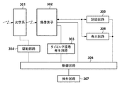
まず、本発明の第1の実施形態における撮像素子について説明する。第1の実施形態の撮像素子は、撮像素子の外部から画像信号を入力し、入力した画像信号に対して撮像素子内部で画像処理を施す機能を有する。
次に、本発明の第2の実施形態について説明する。図7は、第2の実施形態における撮像装置の概略構成を示すブロック図である。図7に示すように、第2の実施形態における撮像装置は、図3に示す撮像装置に、光学系801と第2の撮像素子802とを加えた構成を有する。それ以外の構成は、図3に示すものと同様であるため説明を省略するが、撮像素子302については、第2の撮像素子802と区別するために、第2の実施形態では、第1の撮像素子302と呼ぶ。
次に、本発明の第3の実施形態について説明する。第3の実施形態における撮像素子1400は第1および第2の実施形態における撮像素子302と異なる構成を有する。なお、第3の実施形態における撮像装置は、第1の実施形態で図3を参照して説明した撮像装置、または、第2の実施形態で図8を用いて説明した撮像装置において、撮像素子302が、後述する撮像素子1400に置き換わった構成を有する。それ以外は、第1および第2の実施形態で説明した構成と同様であるため、説明を省略する。
Claims (29)
- 複数の光電変換素子を有する撮像部を備えたイメージセンサであって、
前記イメージセンサの外部から画像データが入力される入力部と、
前記撮像部から得られた画像データおよび前記入力部から入力された画像データに画像処理を施す画像処理部と、
前記画像処理部により画像処理を施された画像データを、外部に出力するための出力部と
を備えることを特徴とするイメージセンサ。 - 前記撮像部、前記入力部、前記画像処理部、前記出力部が1つにパッケージされることを特徴とする請求項1に記載のイメージセンサ。
- 前記撮像部による撮像のタイミングと、前記入力部に前記イメージセンサの外部から画像データが入力されるタイミングが異なることを特徴とする請求項1に記載のイメージセンサ。
- 前記撮像部から得られた画像データを前記画像処理部に供給する供給部を前記入力部とは独立して備えることを特徴とする請求項1に記載のイメージセンサ。
- 前記入力部から入力される画像データは、少なくとも表示、記録、分析のいずれかに用いられることを特徴とする請求項1に記載のイメージセンサ。
- 前記画像処理部は、前記入力部に入力された画像データの現像処理を行うことを特徴とする請求項1に記載のイメージセンサ。
- 前記画像処理部は、前記撮像部から得られた画像データと、前記入力部から入力された画像データとを合成する合成処理を行うことを特徴とする請求項1に記載のイメージセンサ。
- 前記画像処理部は、前記撮像部から得られた画像データと、前記入力部から入力された画像データにそれぞれ異なるゲインをかけて合成することを特徴とする請求項7に記載のイメージセンサ。
- 前記画像処理部は、前記撮像部から得られた画像データと、前記入力部から入力された画像データを平均して合成することを特徴とする請求項7に記載のイメージセンサ。
- 前記画像処理部は、前記撮像部から得られた画像データから、前記入力部から入力された画像データを差分することを特徴とする請求項1に記載のイメージセンサ。
- 複数の光電変換素子毎に前記画像処理部を備えることを特徴とする請求項1に記載のイメージセンサ。
- 予め決められた数の光電変換素子毎に備えられた複数の接続部を有し、
前記画像処理部は、前記複数の接続部それぞれに対して備えられていることを特徴とする請求項11に記載のイメージセンサ。 - 前記入力部を構成する端子と、前記出力部を構成する端子とを、共通の端子により構成したことを特徴とする請求項1に記載のイメージセンサ。
- 前記撮像部と前記画像処理部は、積層された構造を有する互いに異なる基板上に構成され、電気的に接合されていることを特徴とする請求項1に記載のイメージセンサ。
- 請求項1に記載のイメージセンサと、
該イメージセンサから出力された画像データの表示処理部と、
記録処理部と、
を有する撮像装置。 - 複数の光電変換素子を有する撮像部を備えた第1のイメージセンサと、
複数の光電変換素子を有する撮像部を備えた第2のイメージセンサと、を有し、
前記第1のイメージセンサは、外部から画像データが入力される入力部と、前記入力部から入力された画像データに画像処理を施す画像処理部と、前記画像処理部により画像処理を施された画像データを外部に出力するための出力部とを備え、
前記第2のイメージセンサから前記第1のイメージセンサの前記入力部に入力された画像データに前記画像処理部が画像処理を施すことを特徴とする撮像装置。 - 前記第1のイメージセンサおよび前記第2のイメージセンサを制御する制御部をさらに有することを特徴とする請求項16に記載のイメージセンサ。
- 前記第1のイメージセンサは、前記撮像部、前記入力部、前記画像処理部、前記出力部が1つにパッケージされることを特徴とする請求項16に記載のイメージセンサ。
- 前記撮像部による撮像のタイミングと、前記入力部に前記イメージセンサの外部から画像データが入力されるタイミングが異なることを特徴とする請求項16に記載のイメージセンサ。
- 前記入力部から入力される画像データは、少なくとも表示、記録、分析のいずれかに用いられることを特徴とする請求項16に記載のイメージセンサ。
- 前記画像処理部は、前記入力部に入力された画像データの現像処理を行うことを特徴とする請求項16に記載のイメージセンサ。
- 前記画像処理部は、前記第1のイメージセンサから得られる画像データに画像処理を施すことを特徴とする請求項16に記載のイメージセンサ。
- 前記画像処理部は、前記撮像部から得られた画像データと、前記入力部から入力された画像データとを合成する合成処理を行うことを特徴とする請求項16に記載のイメージセンサ。
- 前記第1のイメージセンサにより静止画を撮影し、前記第2のイメージセンサにより動画を撮影することを特徴とする請求項16に記載のイメージセンサ。
- 前記第1のイメージセンサにより動画を撮影し、前記第2のイメージセンサにより静止画を撮影することを特徴とする請求項16に記載のイメージセンサ。
- 前記第1のイメージセンサと前記第2のイメージセンサは、予め決められた視差をもって、同じ被写体を撮影することを特徴とする請求項16に記載のイメージセンサ。
- 前記第1のイメージセンサおよび前記第2のイメージセンサにより、フレームの位相が互いに異なる動画を撮影することを特徴とする請求項16に記載のイメージセンサ。
- 前記第1のイメージセンサの前記撮像部と前記画像処理部は、積層された構造を有する互いに異なる基板上に構成され、電気的に接合されていることを特徴とする請求項16に記載のイメージセンサ。
- さらに前記画像データの表示処理部と、記録処理部とを有することを特徴とする請求項16に記載のイメージセンサ。
Priority Applications (4)
| Application Number | Priority Date | Filing Date | Title |
|---|---|---|---|
| EP16197490.2A EP3174286B1 (en) | 2015-11-25 | 2016-11-07 | Image sensor and image capturing apparatus |
| US15/353,103 US10356314B2 (en) | 2015-11-25 | 2016-11-16 | Image sensor and image capturing apparatus |
| KR1020160156148A KR20170061075A (ko) | 2015-11-25 | 2016-11-23 | 촬상 소자 및 촬상장치 |
| CN201611053766.1A CN107046625B (zh) | 2015-11-25 | 2016-11-25 | 图像传感器和摄像设备 |
Applications Claiming Priority (2)
| Application Number | Priority Date | Filing Date | Title |
|---|---|---|---|
| JP2015230028 | 2015-11-25 | ||
| JP2015230028 | 2015-11-25 |
Publications (3)
| Publication Number | Publication Date |
|---|---|
| JP2017103752A true JP2017103752A (ja) | 2017-06-08 |
| JP2017103752A5 JP2017103752A5 (ja) | 2019-10-17 |
| JP6808409B2 JP6808409B2 (ja) | 2021-01-06 |
Family
ID=59017129
Family Applications (1)
| Application Number | Title | Priority Date | Filing Date |
|---|---|---|---|
| JP2016175882A Active JP6808409B2 (ja) | 2015-11-25 | 2016-09-08 | イメージセンサおよび撮像装置 |
Country Status (3)
| Country | Link |
|---|---|
| JP (1) | JP6808409B2 (ja) |
| KR (1) | KR20170061075A (ja) |
| CN (1) | CN107046625B (ja) |
Cited By (3)
| Publication number | Priority date | Publication date | Assignee | Title |
|---|---|---|---|---|
| JP2018133794A (ja) * | 2017-02-16 | 2018-08-23 | ソニーセミコンダクタソリューションズ株式会社 | 撮像システムおよび撮像装置 |
| JP2019068271A (ja) * | 2017-09-29 | 2019-04-25 | キヤノン株式会社 | 撮像装置、撮像システム、移動体、回路チップ |
| JP2022003817A (ja) * | 2017-09-15 | 2022-01-11 | 株式会社ソニー・インタラクティブエンタテインメント | 撮像装置、画像生成方法およびコンピュータプログラム |
Families Citing this family (1)
| Publication number | Priority date | Publication date | Assignee | Title |
|---|---|---|---|---|
| CN112804467B (zh) * | 2021-04-15 | 2021-06-25 | 北京惠风智慧科技有限公司 | 一种基于多cmos传感器的图像编码方法及装置 |
Citations (8)
| Publication number | Priority date | Publication date | Assignee | Title |
|---|---|---|---|---|
| JPH11266463A (ja) * | 1998-03-18 | 1999-09-28 | Canon Inc | 撮像装置及び撮像システム |
| JP2008079335A (ja) * | 1994-08-22 | 2008-04-03 | Hitachi Ltd | カメラシステムおよびカメラ装置。 |
| JP2008153997A (ja) * | 2006-12-18 | 2008-07-03 | Matsushita Electric Ind Co Ltd | 固体撮像装置、カメラ、車両、監視装置及び固体撮像装置の駆動方法 |
| JP2010141791A (ja) * | 2008-12-15 | 2010-06-24 | Canon Inc | 撮像装置 |
| JP2012018621A (ja) * | 2010-07-09 | 2012-01-26 | Panasonic Corp | 画像処理装置、画像処理方法及びプログラム |
| JP2013183197A (ja) * | 2012-02-29 | 2013-09-12 | Canon Inc | 光電変換装置、および光電変換装置を用いた撮像システム |
| JP2015126043A (ja) * | 2013-12-26 | 2015-07-06 | ソニー株式会社 | 電子デバイス |
| JP2015201834A (ja) * | 2014-03-31 | 2015-11-12 | ソニー株式会社 | 固体撮像装置及びその駆動制御方法、画像処理方法、並びに、電子機器 |
Family Cites Families (5)
| Publication number | Priority date | Publication date | Assignee | Title |
|---|---|---|---|---|
| US6111604A (en) * | 1995-02-21 | 2000-08-29 | Ricoh Company, Ltd. | Digital camera which detects a connection to an external device |
| US20070177025A1 (en) * | 2006-02-01 | 2007-08-02 | Micron Technology, Inc. | Method and apparatus minimizing die area and module size for a dual-camera mobile device |
| US8988558B2 (en) * | 2011-04-26 | 2015-03-24 | Omnivision Technologies, Inc. | Image overlay in a mobile device |
| CN103561213A (zh) * | 2013-11-14 | 2014-02-05 | 深圳市视晶无线技术有限公司 | 一种带辅助摄像头的无线拍摄管理系统 |
| US20150319390A1 (en) * | 2014-04-30 | 2015-11-05 | Sandia Corporation | Stacked and tiled focal plane array |
-
2016
- 2016-09-08 JP JP2016175882A patent/JP6808409B2/ja active Active
- 2016-11-23 KR KR1020160156148A patent/KR20170061075A/ko not_active IP Right Cessation
- 2016-11-25 CN CN201611053766.1A patent/CN107046625B/zh active Active
Patent Citations (8)
| Publication number | Priority date | Publication date | Assignee | Title |
|---|---|---|---|---|
| JP2008079335A (ja) * | 1994-08-22 | 2008-04-03 | Hitachi Ltd | カメラシステムおよびカメラ装置。 |
| JPH11266463A (ja) * | 1998-03-18 | 1999-09-28 | Canon Inc | 撮像装置及び撮像システム |
| JP2008153997A (ja) * | 2006-12-18 | 2008-07-03 | Matsushita Electric Ind Co Ltd | 固体撮像装置、カメラ、車両、監視装置及び固体撮像装置の駆動方法 |
| JP2010141791A (ja) * | 2008-12-15 | 2010-06-24 | Canon Inc | 撮像装置 |
| JP2012018621A (ja) * | 2010-07-09 | 2012-01-26 | Panasonic Corp | 画像処理装置、画像処理方法及びプログラム |
| JP2013183197A (ja) * | 2012-02-29 | 2013-09-12 | Canon Inc | 光電変換装置、および光電変換装置を用いた撮像システム |
| JP2015126043A (ja) * | 2013-12-26 | 2015-07-06 | ソニー株式会社 | 電子デバイス |
| JP2015201834A (ja) * | 2014-03-31 | 2015-11-12 | ソニー株式会社 | 固体撮像装置及びその駆動制御方法、画像処理方法、並びに、電子機器 |
Cited By (4)
| Publication number | Priority date | Publication date | Assignee | Title |
|---|---|---|---|---|
| JP2018133794A (ja) * | 2017-02-16 | 2018-08-23 | ソニーセミコンダクタソリューションズ株式会社 | 撮像システムおよび撮像装置 |
| JP2022003817A (ja) * | 2017-09-15 | 2022-01-11 | 株式会社ソニー・インタラクティブエンタテインメント | 撮像装置、画像生成方法およびコンピュータプログラム |
| JP2019068271A (ja) * | 2017-09-29 | 2019-04-25 | キヤノン株式会社 | 撮像装置、撮像システム、移動体、回路チップ |
| JP7039237B2 (ja) | 2017-09-29 | 2022-03-22 | キヤノン株式会社 | 撮像装置、撮像システム、移動体、回路チップ |
Also Published As
| Publication number | Publication date |
|---|---|
| CN107046625A (zh) | 2017-08-15 |
| KR20170061075A (ko) | 2017-06-02 |
| CN107046625B (zh) | 2020-08-04 |
| JP6808409B2 (ja) | 2021-01-06 |
Similar Documents
| Publication | Publication Date | Title |
|---|---|---|
| US11206353B2 (en) | Electronic apparatus, method for controlling electronic apparatus, and control program for setting image-capture conditions of image sensor | |
| JP5317591B2 (ja) | 撮像装置 | |
| TWI617196B (zh) | 圖像感測器、成像裝置、行動終端及成像方法 | |
| WO2017101451A1 (zh) | 成像方法、成像装置及电子装置 | |
| JP6808409B2 (ja) | イメージセンサおよび撮像装置 | |
| EP3174286B1 (en) | Image sensor and image capturing apparatus | |
| US20240089402A1 (en) | Electronic apparatus, reproduction device, reproduction method, recording medium, and recording method | |
| JP2017098791A (ja) | 撮像素子および撮像装置 | |
| CN104041004A (zh) | 摄像设备及其控制方法和摄像系统 | |
| CN109474781A (zh) | 摄像装置、摄像装置的控制方法、记录介质 | |
| JP2010062639A (ja) | 撮像装置 | |
| KR102117858B1 (ko) | 고체 촬상 소자 및 촬상장치 | |
| TW201724846A (zh) | 圖像感測器及具有其的終端、成像方法 | |
| US20170318256A1 (en) | Electronic apparatus, reproduction device, reproduction method, recording medium, and recording method | |
| US10686987B2 (en) | Electronic apparatus with image capturing unit having first and second imaging regions that capture an image of a subject under differing imaging conditions | |
| US20170324911A1 (en) | Electronic apparatus, reproduction device, reproduction method, recording medium, and recording method | |
| JP2005303653A (ja) | 撮像装置 | |
| WO2020203799A1 (ja) | 撮像素子、及び、撮像装置 | |
| JP5726244B2 (ja) | 撮像装置及び撮像方法 | |
| CN117135480A (zh) | 影像感测装置 | |
| JP2023054229A (ja) | 電子機器 | |
| JP2020057877A (ja) | 電子機器および設定プログラム | |
| JP2015128256A (ja) | 画像処理装置、画像処理方法、撮像装置および撮像素子 | |
| JP2017055360A (ja) | 撮像装置、画像処理装置及びそれらの制御方法 | |
| JP2004297563A (ja) | 撮像素子の駆動方法 |
Legal Events
| Date | Code | Title | Description |
|---|---|---|---|
| A521 | Request for written amendment filed |
Free format text: JAPANESE INTERMEDIATE CODE: A523 Effective date: 20190905 |
|
| A621 | Written request for application examination |
Free format text: JAPANESE INTERMEDIATE CODE: A621 Effective date: 20190905 |
|
| A977 | Report on retrieval |
Free format text: JAPANESE INTERMEDIATE CODE: A971007 Effective date: 20200608 |
|
| A131 | Notification of reasons for refusal |
Free format text: JAPANESE INTERMEDIATE CODE: A131 Effective date: 20200622 |
|
| A521 | Request for written amendment filed |
Free format text: JAPANESE INTERMEDIATE CODE: A523 Effective date: 20200717 |
|
| A131 | Notification of reasons for refusal |
Free format text: JAPANESE INTERMEDIATE CODE: A131 Effective date: 20200811 |
|
| A521 | Request for written amendment filed |
Free format text: JAPANESE INTERMEDIATE CODE: A523 Effective date: 20201008 |
|
| TRDD | Decision of grant or rejection written | ||
| A01 | Written decision to grant a patent or to grant a registration (utility model) |
Free format text: JAPANESE INTERMEDIATE CODE: A01 Effective date: 20201109 |
|
| A61 | First payment of annual fees (during grant procedure) |
Free format text: JAPANESE INTERMEDIATE CODE: A61 Effective date: 20201209 |
|
| R151 | Written notification of patent or utility model registration |
Ref document number: 6808409 Country of ref document: JP Free format text: JAPANESE INTERMEDIATE CODE: R151 |