JP2017103366A - Electronic component module and manufacturing method therefor - Google Patents
Electronic component module and manufacturing method therefor Download PDFInfo
- Publication number
- JP2017103366A JP2017103366A JP2015235905A JP2015235905A JP2017103366A JP 2017103366 A JP2017103366 A JP 2017103366A JP 2015235905 A JP2015235905 A JP 2015235905A JP 2015235905 A JP2015235905 A JP 2015235905A JP 2017103366 A JP2017103366 A JP 2017103366A
- Authority
- JP
- Japan
- Prior art keywords
- substrate
- electronic component
- substrate portion
- component module
- fixed
- Prior art date
- Legal status (The legal status is an assumption and is not a legal conclusion. Google has not performed a legal analysis and makes no representation as to the accuracy of the status listed.)
- Pending
Links
Images


Classifications
-
- H—ELECTRICITY
- H01—ELECTRIC ELEMENTS
- H01L—SEMICONDUCTOR DEVICES NOT COVERED BY CLASS H10
- H01L23/00—Details of semiconductor or other solid state devices
- H01L23/52—Arrangements for conducting electric current within the device in operation from one component to another, i.e. interconnections, e.g. wires, lead frames
- H01L23/538—Arrangements for conducting electric current within the device in operation from one component to another, i.e. interconnections, e.g. wires, lead frames the interconnection structure between a plurality of semiconductor chips being formed on, or in, insulating substrates
- H01L23/5387—Flexible insulating substrates
-
- H—ELECTRICITY
- H01—ELECTRIC ELEMENTS
- H01L—SEMICONDUCTOR DEVICES NOT COVERED BY CLASS H10
- H01L23/00—Details of semiconductor or other solid state devices
- H01L23/34—Arrangements for cooling, heating, ventilating or temperature compensation ; Temperature sensing arrangements
- H01L23/36—Selection of materials, or shaping, to facilitate cooling or heating, e.g. heatsinks
- H01L23/367—Cooling facilitated by shape of device
-
- H—ELECTRICITY
- H01—ELECTRIC ELEMENTS
- H01L—SEMICONDUCTOR DEVICES NOT COVERED BY CLASS H10
- H01L23/00—Details of semiconductor or other solid state devices
- H01L23/12—Mountings, e.g. non-detachable insulating substrates
- H01L23/13—Mountings, e.g. non-detachable insulating substrates characterised by the shape
-
- H—ELECTRICITY
- H01—ELECTRIC ELEMENTS
- H01L—SEMICONDUCTOR DEVICES NOT COVERED BY CLASS H10
- H01L23/00—Details of semiconductor or other solid state devices
- H01L23/12—Mountings, e.g. non-detachable insulating substrates
- H01L23/14—Mountings, e.g. non-detachable insulating substrates characterised by the material or its electrical properties
-
- H—ELECTRICITY
- H01—ELECTRIC ELEMENTS
- H01L—SEMICONDUCTOR DEVICES NOT COVERED BY CLASS H10
- H01L23/00—Details of semiconductor or other solid state devices
- H01L23/34—Arrangements for cooling, heating, ventilating or temperature compensation ; Temperature sensing arrangements
- H01L23/36—Selection of materials, or shaping, to facilitate cooling or heating, e.g. heatsinks
-
- H—ELECTRICITY
- H01—ELECTRIC ELEMENTS
- H01L—SEMICONDUCTOR DEVICES NOT COVERED BY CLASS H10
- H01L23/00—Details of semiconductor or other solid state devices
- H01L23/34—Arrangements for cooling, heating, ventilating or temperature compensation ; Temperature sensing arrangements
- H01L23/40—Mountings or securing means for detachable cooling or heating arrangements ; fixed by friction, plugs or springs
-
- H—ELECTRICITY
- H01—ELECTRIC ELEMENTS
- H01L—SEMICONDUCTOR DEVICES NOT COVERED BY CLASS H10
- H01L23/00—Details of semiconductor or other solid state devices
- H01L23/52—Arrangements for conducting electric current within the device in operation from one component to another, i.e. interconnections, e.g. wires, lead frames
- H01L23/538—Arrangements for conducting electric current within the device in operation from one component to another, i.e. interconnections, e.g. wires, lead frames the interconnection structure between a plurality of semiconductor chips being formed on, or in, insulating substrates
- H01L23/5385—Assembly of a plurality of insulating substrates
-
- H—ELECTRICITY
- H01—ELECTRIC ELEMENTS
- H01L—SEMICONDUCTOR DEVICES NOT COVERED BY CLASS H10
- H01L25/00—Assemblies consisting of a plurality of individual semiconductor or other solid state devices ; Multistep manufacturing processes thereof
- H01L25/03—Assemblies consisting of a plurality of individual semiconductor or other solid state devices ; Multistep manufacturing processes thereof all the devices being of a type provided for in the same subgroup of groups H01L27/00 - H01L33/00, or in a single subclass of H10K, H10N, e.g. assemblies of rectifier diodes
- H01L25/04—Assemblies consisting of a plurality of individual semiconductor or other solid state devices ; Multistep manufacturing processes thereof all the devices being of a type provided for in the same subgroup of groups H01L27/00 - H01L33/00, or in a single subclass of H10K, H10N, e.g. assemblies of rectifier diodes the devices not having separate containers
- H01L25/065—Assemblies consisting of a plurality of individual semiconductor or other solid state devices ; Multistep manufacturing processes thereof all the devices being of a type provided for in the same subgroup of groups H01L27/00 - H01L33/00, or in a single subclass of H10K, H10N, e.g. assemblies of rectifier diodes the devices not having separate containers the devices being of a type provided for in group H01L27/00
- H01L25/0652—Assemblies consisting of a plurality of individual semiconductor or other solid state devices ; Multistep manufacturing processes thereof all the devices being of a type provided for in the same subgroup of groups H01L27/00 - H01L33/00, or in a single subclass of H10K, H10N, e.g. assemblies of rectifier diodes the devices not having separate containers the devices being of a type provided for in group H01L27/00 the devices being arranged next and on each other, i.e. mixed assemblies
-
- H—ELECTRICITY
- H01—ELECTRIC ELEMENTS
- H01L—SEMICONDUCTOR DEVICES NOT COVERED BY CLASS H10
- H01L25/00—Assemblies consisting of a plurality of individual semiconductor or other solid state devices ; Multistep manufacturing processes thereof
- H01L25/03—Assemblies consisting of a plurality of individual semiconductor or other solid state devices ; Multistep manufacturing processes thereof all the devices being of a type provided for in the same subgroup of groups H01L27/00 - H01L33/00, or in a single subclass of H10K, H10N, e.g. assemblies of rectifier diodes
- H01L25/04—Assemblies consisting of a plurality of individual semiconductor or other solid state devices ; Multistep manufacturing processes thereof all the devices being of a type provided for in the same subgroup of groups H01L27/00 - H01L33/00, or in a single subclass of H10K, H10N, e.g. assemblies of rectifier diodes the devices not having separate containers
- H01L25/07—Assemblies consisting of a plurality of individual semiconductor or other solid state devices ; Multistep manufacturing processes thereof all the devices being of a type provided for in the same subgroup of groups H01L27/00 - H01L33/00, or in a single subclass of H10K, H10N, e.g. assemblies of rectifier diodes the devices not having separate containers the devices being of a type provided for in group H01L29/00
-
- H—ELECTRICITY
- H01—ELECTRIC ELEMENTS
- H01L—SEMICONDUCTOR DEVICES NOT COVERED BY CLASS H10
- H01L25/00—Assemblies consisting of a plurality of individual semiconductor or other solid state devices ; Multistep manufacturing processes thereof
- H01L25/03—Assemblies consisting of a plurality of individual semiconductor or other solid state devices ; Multistep manufacturing processes thereof all the devices being of a type provided for in the same subgroup of groups H01L27/00 - H01L33/00, or in a single subclass of H10K, H10N, e.g. assemblies of rectifier diodes
- H01L25/10—Assemblies consisting of a plurality of individual semiconductor or other solid state devices ; Multistep manufacturing processes thereof all the devices being of a type provided for in the same subgroup of groups H01L27/00 - H01L33/00, or in a single subclass of H10K, H10N, e.g. assemblies of rectifier diodes the devices having separate containers
-
- H—ELECTRICITY
- H05—ELECTRIC TECHNIQUES NOT OTHERWISE PROVIDED FOR
- H05K—PRINTED CIRCUITS; CASINGS OR CONSTRUCTIONAL DETAILS OF ELECTRIC APPARATUS; MANUFACTURE OF ASSEMBLAGES OF ELECTRICAL COMPONENTS
- H05K1/00—Printed circuits
- H05K1/02—Details
- H05K1/0201—Thermal arrangements, e.g. for cooling, heating or preventing overheating
- H05K1/0203—Cooling of mounted components
-
- H—ELECTRICITY
- H05—ELECTRIC TECHNIQUES NOT OTHERWISE PROVIDED FOR
- H05K—PRINTED CIRCUITS; CASINGS OR CONSTRUCTIONAL DETAILS OF ELECTRIC APPARATUS; MANUFACTURE OF ASSEMBLAGES OF ELECTRICAL COMPONENTS
- H05K1/00—Printed circuits
- H05K1/02—Details
- H05K1/0266—Marks, test patterns or identification means
- H05K1/0268—Marks, test patterns or identification means for electrical inspection or testing
-
- H—ELECTRICITY
- H05—ELECTRIC TECHNIQUES NOT OTHERWISE PROVIDED FOR
- H05K—PRINTED CIRCUITS; CASINGS OR CONSTRUCTIONAL DETAILS OF ELECTRIC APPARATUS; MANUFACTURE OF ASSEMBLAGES OF ELECTRICAL COMPONENTS
- H05K3/00—Apparatus or processes for manufacturing printed circuits
- H05K3/46—Manufacturing multilayer circuits
- H05K3/4611—Manufacturing multilayer circuits by laminating two or more circuit boards
-
- H—ELECTRICITY
- H01—ELECTRIC ELEMENTS
- H01L—SEMICONDUCTOR DEVICES NOT COVERED BY CLASS H10
- H01L2224/00—Indexing scheme for arrangements for connecting or disconnecting semiconductor or solid-state bodies and methods related thereto as covered by H01L24/00
- H01L2224/01—Means for bonding being attached to, or being formed on, the surface to be connected, e.g. chip-to-package, die-attach, "first-level" interconnects; Manufacturing methods related thereto
- H01L2224/10—Bump connectors; Manufacturing methods related thereto
- H01L2224/15—Structure, shape, material or disposition of the bump connectors after the connecting process
- H01L2224/16—Structure, shape, material or disposition of the bump connectors after the connecting process of an individual bump connector
- H01L2224/161—Disposition
- H01L2224/16151—Disposition the bump connector connecting between a semiconductor or solid-state body and an item not being a semiconductor or solid-state body, e.g. chip-to-substrate, chip-to-passive
- H01L2224/16221—Disposition the bump connector connecting between a semiconductor or solid-state body and an item not being a semiconductor or solid-state body, e.g. chip-to-substrate, chip-to-passive the body and the item being stacked
- H01L2224/16225—Disposition the bump connector connecting between a semiconductor or solid-state body and an item not being a semiconductor or solid-state body, e.g. chip-to-substrate, chip-to-passive the body and the item being stacked the item being non-metallic, e.g. insulating substrate with or without metallisation
-
- H—ELECTRICITY
- H01—ELECTRIC ELEMENTS
- H01L—SEMICONDUCTOR DEVICES NOT COVERED BY CLASS H10
- H01L2225/00—Details relating to assemblies covered by the group H01L25/00 but not provided for in its subgroups
- H01L2225/03—All the devices being of a type provided for in the same subgroup of groups H01L27/00 - H01L33/648 and H10K99/00
- H01L2225/04—All the devices being of a type provided for in the same subgroup of groups H01L27/00 - H01L33/648 and H10K99/00 the devices not having separate containers
- H01L2225/065—All the devices being of a type provided for in the same subgroup of groups H01L27/00 - H01L33/648 and H10K99/00 the devices not having separate containers the devices being of a type provided for in group H01L27/00
- H01L2225/06503—Stacked arrangements of devices
- H01L2225/06579—TAB carriers; beam leads
-
- H—ELECTRICITY
- H01—ELECTRIC ELEMENTS
- H01L—SEMICONDUCTOR DEVICES NOT COVERED BY CLASS H10
- H01L2225/00—Details relating to assemblies covered by the group H01L25/00 but not provided for in its subgroups
- H01L2225/03—All the devices being of a type provided for in the same subgroup of groups H01L27/00 - H01L33/648 and H10K99/00
- H01L2225/04—All the devices being of a type provided for in the same subgroup of groups H01L27/00 - H01L33/648 and H10K99/00 the devices not having separate containers
- H01L2225/065—All the devices being of a type provided for in the same subgroup of groups H01L27/00 - H01L33/648 and H10K99/00 the devices not having separate containers the devices being of a type provided for in group H01L27/00
- H01L2225/06503—Stacked arrangements of devices
- H01L2225/06589—Thermal management, e.g. cooling
-
- H—ELECTRICITY
- H05—ELECTRIC TECHNIQUES NOT OTHERWISE PROVIDED FOR
- H05K—PRINTED CIRCUITS; CASINGS OR CONSTRUCTIONAL DETAILS OF ELECTRIC APPARATUS; MANUFACTURE OF ASSEMBLAGES OF ELECTRICAL COMPONENTS
- H05K2201/00—Indexing scheme relating to printed circuits covered by H05K1/00
- H05K2201/03—Conductive materials
- H05K2201/0332—Structure of the conductor
- H05K2201/0388—Other aspects of conductors
-
- H—ELECTRICITY
- H05—ELECTRIC TECHNIQUES NOT OTHERWISE PROVIDED FOR
- H05K—PRINTED CIRCUITS; CASINGS OR CONSTRUCTIONAL DETAILS OF ELECTRIC APPARATUS; MANUFACTURE OF ASSEMBLAGES OF ELECTRICAL COMPONENTS
- H05K2203/00—Indexing scheme relating to apparatus or processes for manufacturing printed circuits covered by H05K3/00
- H05K2203/06—Lamination
- H05K2203/063—Lamination of preperforated insulating layer
-
- H—ELECTRICITY
- H05—ELECTRIC TECHNIQUES NOT OTHERWISE PROVIDED FOR
- H05K—PRINTED CIRCUITS; CASINGS OR CONSTRUCTIONAL DETAILS OF ELECTRIC APPARATUS; MANUFACTURE OF ASSEMBLAGES OF ELECTRICAL COMPONENTS
- H05K2203/00—Indexing scheme relating to apparatus or processes for manufacturing printed circuits covered by H05K3/00
- H05K2203/30—Details of processes not otherwise provided for in H05K2203/01 - H05K2203/17
- H05K2203/302—Bending a rigid substrate; Breaking rigid substrates by bending
Abstract
Description
本発明は、複数の電子部品が一体化された電子部品モジュールおよびその製造方法に関するものである。 The present invention relates to an electronic component module in which a plurality of electronic components are integrated and a method for manufacturing the same.
特許文献1に、基板内に電子部品を内蔵した部品内蔵基板が開示されている。
また、部品内蔵基板の製造方法として、電子部品が表面実装された表面実装基板を製造した後に、表面実装基板を封止するための複数の封止用基板を順次積層する方法がある。 As a method for manufacturing a component-embedded substrate, there is a method in which a surface mounting substrate on which electronic components are surface mounted is manufactured, and then a plurality of sealing substrates for sealing the surface mounting substrate are sequentially stacked.
上記した部品内蔵基板の製造方法では、表面実装基板を製造する工程に加えて、複数の封止用基板を積層する工程が必要となる。このため、従来の表面実装基板を製造する際と比較して、製造時間が大幅に長くなってしまう。 The above-described method for manufacturing a component-embedded substrate requires a step of laminating a plurality of sealing substrates in addition to the step of manufacturing the surface mount substrate. For this reason, compared with the case of manufacturing the conventional surface mount substrate, the manufacturing time is significantly increased.
また、従来の部品内蔵基板においては、内蔵された電子部品の放熱性の向上が求められている。 Further, in the conventional component-embedded substrate, it is required to improve heat dissipation of the built-in electronic component.
本発明は上記点に鑑みて、従来の部品内蔵基板と比較して、製造時間の短縮化と放熱性の向上が可能な電子部品モジュールおよびその製造方法を提供することを目的とする。 The present invention has been made in view of the above points, and it is an object of the present invention to provide an electronic component module capable of shortening the manufacturing time and improving heat dissipation as compared with a conventional component-embedded substrate, and a method for manufacturing the same.
上記目的を達成するため、請求項1に記載の発明は、
複数の電子部品が一体化された電子部品モジュールであって、
基板(10)と、
基板の表面(11a、12a)に実装された複数の電子部品(21、22)と、
基板に固定され、金属で構成された放熱板(30)とを備え、
基板は、第1基板部(11)と、第2基板部(12)と、第3基板部(13)とを有し、
複数の電子部品は、第1基板部の一面(11a)に実装された1つ以上の第1部品(21)と、第2基板部の一面(12a)に実装された1つ以上の第2部品(22)とを有し、
第1基板部と第2基板部は、第1基板部の一面と第2基板部の一面とを向かい合わせにして配置されており、
第3基板部が第1基板部と第2基板部の間に配置されることにより、第1基板部と、第3基板部と、第2基板部とが連なっており、
放熱板は、第1基板部、第2基板部、第3基板部の少なくとも1つ以上に固定された固定部(31、32、33)と、第1基板部と第2基板部に挟まれた領域(R1)の側方に位置する側方部(34、35、36)とを有し、
側方部は、屈曲した形状の屈曲部を介して、固定部と連なっている。
In order to achieve the above object, the invention described in
An electronic component module in which a plurality of electronic components are integrated,
A substrate (10);
A plurality of electronic components (21, 22) mounted on the surface (11a, 12a) of the substrate;
A heat sink (30) made of metal and fixed to the substrate,
The substrate has a first substrate portion (11), a second substrate portion (12), and a third substrate portion (13),
The plurality of electronic components include one or more first components (21) mounted on one surface (11a) of the first substrate unit and one or more second components mounted on one surface (12a) of the second substrate unit. Parts (22),
The first substrate portion and the second substrate portion are arranged with one surface of the first substrate portion facing one surface of the second substrate portion,
By arranging the third substrate unit between the first substrate unit and the second substrate unit, the first substrate unit, the third substrate unit, and the second substrate unit are connected,
The heat sink is sandwiched between the first substrate unit, the second substrate unit, the fixed unit (31, 32, 33) fixed to at least one of the first substrate unit, the second substrate unit, and the third substrate unit. Side portions (34, 35, 36) located on the sides of the region (R1),
The side portion is connected to the fixed portion via a bent portion having a bent shape.
この電子部品モジュールは、第1基板部と第2基板部の表面に複数の電子部品を実装した後に、基板と放熱板を折り曲げることで、製造される。すなわち、この電子部品モジュールは、表面実装基板を製造した後に、表面実装基板を折り曲げることで、製造される。したがって、表面実装基板を製造した後に、複数の封止用基板を積層する場合と比較して、製造時間を短縮できる。 This electronic component module is manufactured by bending a substrate and a heat sink after mounting a plurality of electronic components on the surfaces of the first substrate portion and the second substrate portion. That is, the electronic component module is manufactured by bending the surface mounting substrate after manufacturing the surface mounting substrate. Therefore, the manufacturing time can be shortened as compared with the case where a plurality of sealing substrates are stacked after the surface mounting substrate is manufactured.
さらに、この電子部品モジュールは、第1基板部と第2基板部に挟まれた領域の側方に放熱板の一部が配置されている。このため、第1基板部と第2基板部に挟まれた領域の側方に放熱板が配置されていない場合と比較して、電子部品の放熱性を向上できる。 Further, in this electronic component module, a part of the heat radiating plate is disposed on the side of the region sandwiched between the first substrate portion and the second substrate portion. For this reason, compared with the case where the heat sink is not arrange | positioned at the side of the area | region pinched | interposed between the 1st board | substrate part and the 2nd board | substrate part, the heat dissipation of an electronic component can be improved.
また、請求項5に記載の発明は、
複数の電子部品が一体化された電子部品モジュールの製造方法であって、
放熱板(30)が固定された基板(10)を準備することと、
基板の表面(11a、12a)に複数の電子部品(21、22)を実装することと、
実装された基板および放熱板のそれぞれを折り曲げることとを備え、
準備される基板は、第1基板部(11)と、第2基板部(12)と、第1基板部と第2基板部の両方に連なる第3基板部(13)とを有し、
基板に固定された放熱板は、第1基板部、第2基板部、第3基板部の少なくとも1つ以上に重なって固定された固定部(31、32、33)と、固定部に連なっており、第1基板部、第2基板部、第3基板部のいずれとも重なっていない側方部(34、35、36)とを有し、
実装することは、第1基板部の一面(11a)に1つ以上の第1部品(21)を実装することと、第2基板部の一面(12a)に1つ以上の第2部品(22)を実装することとを含み、
折り曲げることは、基板を折り曲げて、第1基板部の一面と第2基板部の一面とを向かい合わせに配置するとともに、第1基板部と第2基板部の間を連ねる第3基板部を構成することと、側方部を折り曲げて、第1基板部と第2基板部に挟まれた領域(R1)の側方に側方部を位置させることとを含む。
The invention according to claim 5
A method of manufacturing an electronic component module in which a plurality of electronic components are integrated,
Preparing a substrate (10) to which a heat sink (30) is fixed;
Mounting a plurality of electronic components (21, 22) on the surface (11a, 12a) of the substrate;
Folding each of the mounted substrate and the heat sink,
The prepared substrate has a first substrate unit (11), a second substrate unit (12), and a third substrate unit (13) connected to both the first substrate unit and the second substrate unit,
The heat sink fixed to the substrate is connected to the fixed portion (31, 32, 33) fixed to overlap at least one of the first substrate portion, the second substrate portion, and the third substrate portion, and to the fixed portion. And side portions (34, 35, 36) that do not overlap any of the first substrate portion, the second substrate portion, and the third substrate portion,
The mounting includes mounting one or more first components (21) on one surface (11a) of the first substrate portion and one or more second components (22 on one surface (12a) of the second substrate portion. )
Bending means that the substrate is bent so that one surface of the first substrate portion and one surface of the second substrate portion face each other, and the third substrate portion that connects between the first substrate portion and the second substrate portion is formed. And bending the side portion to position the side portion on the side of the region (R1) sandwiched between the first substrate portion and the second substrate portion.
この電子部品モジュールの製造方法では、表面実装基板を製造した後に、表面実装基板の折り曲げを行う。このため、表面実装基板を製造した後に、複数の封止用基板を積層する場合と比較して、製造時間を短縮できる。 In this method of manufacturing an electronic component module, after the surface mount substrate is manufactured, the surface mount substrate is bent. For this reason, manufacturing time can be shortened compared with the case where a plurality of substrates for sealing are laminated after manufacturing a surface mount substrate.
さらに、この電子部品モジュールの製造方法によれば、放熱板を折り曲げることにより、第1基板部と第2基板部に挟まれた領域の側方に放熱板の一部を配置している。このため、第1基板部と第2基板部に挟まれた領域の側方に放熱板が配置されていない場合と比較して、電子部品の放熱性を向上できる。 Furthermore, according to this method for manufacturing an electronic component module, a part of the heat dissipation plate is disposed on the side of the region sandwiched between the first substrate portion and the second substrate portion by bending the heat dissipation plate. For this reason, compared with the case where the heat sink is not arrange | positioned at the side of the area | region pinched | interposed between the 1st board | substrate part and the 2nd board | substrate part, the heat dissipation of an electronic component can be improved.
なお、この欄および特許請求の範囲で記載した各手段の括弧内の符号は、後述する実施形態に記載の具体的手段との対応関係を示す一例である。 In addition, the code | symbol in the bracket | parenthesis of each means described in this column and the claim is an example which shows a corresponding relationship with the specific means as described in embodiment mentioned later.
以下、本発明の実施形態について図に基づいて説明する。なお、以下の各実施形態相互において、互いに同一もしくは均等である部分には、同一符号を付して説明を行う。 Hereinafter, embodiments of the present invention will be described with reference to the drawings. In the following embodiments, parts that are the same or equivalent to each other will be described with the same reference numerals.
(第1実施形態)
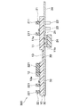
図1、2、3に示すように、本実施形態の電子部品モジュール1は、複数の電子部品が一体化した状態で、マザーボード2に搭載される。電子部品モジュール1は、複数の電子部品が擬似的に内蔵された部品内蔵基板を実現したものである。
(First embodiment)
As shown in FIGS. 1, 2, and 3, the
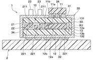
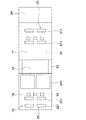
具体的には、図2に示すように、電子部品モジュール1は、1つのプリント配線基板10と、複数の電子部品21、22、23、24と、放熱板30とを備えている。
Specifically, as shown in FIG. 2, the
プリント配線基板10は、第1基板部11と、第2基板部12と、第3基板部13とを有している。
The printed
第1基板部11と第2基板部12は、平板状である。第3基板部13は、第1基板部11と第2基板部12の両方に連なっている。第3基板部13のうち第1基板部11側の一部131と第2基板部12側の一部132は、屈曲した形状の屈曲部となっている。本実施形態では、第3基板部13のうち第1基板部11側の一部131と第2基板部12側の一部132は、それぞれ、直角に屈曲している。第3基板部13のうち第1基板部11側の一部131と第2基板部12側の一部132の間の部分は、平板形状である。
The
第3基板部13は、第1基板部11および第2基板部12よりも薄くされている。これにより、第3基板部13は、第1基板部11および第2基板部12よりも柔軟性を有している。第1基板部11および第2基板部12は、第3基板部13よりも厚くされている。これにより、第1基板部11および第2基板部12は、第3基板部13よりも固くされている。
The
複数の電子部品は、第1基板部11の一面11aに実装された複数の第1部品21と、第2基板部12の一面12aに実装された複数の第2部品22とを有している。
The plurality of electronic components include a plurality of
第1基板部11と第2基板部12は、実装されている一面11aと一面12aとを向かい合わせにして配置されている。第1基板部11の平面形状と第2基板部12の平面形状は、同じ四角形である。
The
複数の第1部品21の中で背の高い部品211と、第2部品22の中で背の高い部品221とは、第1基板部11の一面11aに平行な方向で、互いに異なる位置に配置されている。
The
放熱板30は、第1基板部11、第2基板部12および第3基板部13に固定された固定部と、第1基板部11と第2基板部12に挟まれた領域R1の側方に位置する側方部とを有する。固定部は、第1基板部11、第2基板部12および第3基板部13に重なっている。側方部は、第1基板部11、第2基板部12および第3基板部13に重なっていない。なお、領域R1の側方とは、第1基板部11と第2基板部12の並び方向に対する側方のことである。すなわち、領域R1の側方とは、第1基板部11と第2基板部12の並び方向を上下方向としたときの横方向のことである。換言すると、領域R1の側方は、第1基板部11と第2基板部12の並び方向に対して交差する方向である。また、領域R1の側方に位置するとは、領域R1のうち第1基板部11および第2基板部12に囲まれていない領域R1の周囲に位置することと同じ意味である。
The
固定部は、第1固定部31と、第2固定部32と、第3固定部33とを有する。第1固定部31は、第1基板部11の一面11aとは反対側の他面11bに固定されている。第2固定部32は、第2基板部12の一面12aとは反対側の他面12bに固定されている。第3固定部33は、第3基板部13の一面13aとは反対側の他面13bに固定されている。第1固定部31、第2固定部32、第3固定部33のそれぞれの平面形状は、第1基板部11、第2基板部12、第3基板部13のそれぞれの平面形状と同じ四角形である。図1に示すように、第3固定部33は、第1固定部31の一辺に連なっている。
The fixing part includes a first fixing
図1に示すように、側方部は、第1固定部31の他の三辺のそれぞれに連なる第1側方部34と、第2側方部35と、第3側方部36とを有する。図2に示すように、第1側方部34は、第1固定部31側の一部が屈曲した形状の屈曲部となっている。第1側方部34は、屈曲部を除く部分が平板形状である。第2側方部35と第3側方部36も、第1側方部34と同様の形状である。
As shown in FIG. 1, the side portion includes a
図3に示すように、第3側方部36は、電子部品モジュール1の側面に位置している。第1側方部34と第2側方部35も、第3側方部36と同様に、電子部品モジュール1の側面に位置している。
As shown in FIG. 3, the
換言すると、図2に示すように、第1側方部34は、第1部品21および第2部品22が配置されている第1基板部11と第2基板部12の間の領域R1の側方および第2基板部12の側方に位置している。第1側方部34は、少なくとも領域R1の側方に位置していればよい。したがって、第1基板部11と第2基板部12が対向する方向(すなわち、図2では上下方向)での第1側方部34の長さは、第1基板部11と第2基板部12が対向する方向での第1基板部11と第2基板部12の間隔以上であればよい。第2側方部35と第3側方部36も、第1側方部34と同様に、領域R1の側方に位置している。
In other words, as shown in FIG. 2, the
放熱板30のうち第1固定部31と第2固定部32が、領域R1に対して、第1基板部と第2基板部の並び方向での両側に配置されている。放熱板30のうち第1側方部34、第2側方部35、第3側方部36および第3固定部33は、領域R1の周囲全域に配置されている。したがって、放熱板30は、領域R1を、六方向から囲んでいる。
The 1st fixing | fixed
放熱板30は、金属で構成されている。第1側方部34、第2側方部35および第3側方部36は、それぞれの全域において金属面が露出している。放熱板30は、プリント配線基板10の図示しないグランド電極と電気的に接続されている。これにより、放熱板30は、グランド電位とされる。
The
また、複数の電子部品は、第1基板部11の一面11aとは反対側の他面11bに実装された電子部品23、24を有している。
The plurality of electronic components have
次に、本実施形態の電子部品モジュール1の製造方法について説明する。
Next, the manufacturing method of the
図4に示すように、電子部品モジュール1の製造方法は、基板の準備工程と、基板に複数の電子部品を実装して実装基板を製造する実装工程と、実装基板を折り曲げる折り曲げ工程とを順に行う。
As shown in FIG. 4, the manufacturing method of the
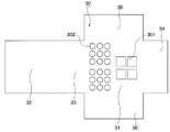
準備工程では、図5、6に示すように、放熱板30が固定されたプリント配線基板10を準備する。放熱板30が固定されたプリント配線基板10は、図7に示す平板状の1枚の放熱板30と、図8に示す平板状の1枚のプリント配線基板10とが固定されたものである。放熱板30は、プリント配線基板10よりも大きな形状である。放熱板30は、側方部34、35、36がプリント配線基板10と重なっていない状態で、プリント配線基板10に固定されている。放熱板30は、銅箔等の金属箔で構成されている。放熱板30は、後述する導体パターン102よりも厚くされている。
In the preparation step, as shown in FIGS. 5 and 6, the printed
図7に示すように、放熱板30には、電子部品23、24を実装するための開口部301、302が形成されている。
As shown in FIG. 7,
図8に示すように、プリント配線基板10は、第1基板部11と第2基板部12と第3基板部13とを有している。
As shown in FIG. 8, the printed
図9は、図8のプリント配線基板10の具体的な断面構造を示している。図9に示すように、プリント配線基板10は、複数のフィルム状の絶縁基材101が積層されている。絶縁基材101は、表面に1つ以上の導体パターン102が形成されている。導体パターン102は、銅箔等の金属箔で構成されている。絶縁基材101は、内部に1つ以上のビア103が形成されている。導体パターン102およびビア103が配線を構成している。絶縁基材101は、熱可塑性樹脂で構成されている。絶縁基材101は、熱可塑性樹脂以外の樹脂材料で構成されていてもよい。絶縁基材101は、樹脂材料のみで構成されている場合に限られず、樹脂材料以外の材料が含まれていてもよい。
FIG. 9 shows a specific cross-sectional structure of the printed
第3基板部13は、第1基板部11および第2基板部12よりも絶縁基材101の積層数が少なくされている。これにより、第3基板部13は、第1基板部11および第2基板部12よりも薄くされている。
The
図10に示すように、導体パターン102やビア103が形成された複数の絶縁基材101と放熱板30とを積層して積層体200を形成する。その後、積層体200を加熱加圧する。これにより、複数の絶縁基材101同士が接合されてプリント配線基板10が形成される。さらに、図5、6に示すように、放熱板30がプリント配線基板10の表面に接合される。
As shown in FIG. 10, a
実装工程では、図5、6に示すように、プリント配線基板10の表面11a、12a、11bに複数の電子部品21、22、23、24を実装する。これにより、プリント配線基板10の表面に複数の電子部品21、22、23、24が実装された表面実装基板300が製造される。
In the mounting process, as shown in FIGS. 5 and 6, a plurality of
折り曲げ工程では、図1〜3に示す形状となるように、図5、6に示す表面実装基板300を折り曲げる。具体的には、第3基板部13を第3固定部33とともに折り曲げる。その後、放熱板30の第1側方部34、第2側方部35、第3側方部36を折り曲げる。なお、各側方部34、35、36を折り曲げた後に、第3基板部13を折り曲げてもよい。放熱板30を折り曲げた後、第1側方部34、第2側方部35および第3側方部36を、第2基板部12の側面に接合する。
In the bending step, the
このようにして、本実施形態の電子部品モジュール1が製造される。その後、電子部品モジュール1は、図2、3に示すように、半田付けされて、マザーボード2に実装される。
In this way, the
次に、本実施形態の効果について説明する。 Next, the effect of this embodiment will be described.
(1)本実施形態の電子部品モジュール1は、第1基板部11と第2基板部12の表面11a、12aに複数の電子部品21、22を実装した後に、第3基板部13と側方部34、35、36を折り曲げることで、製造される。すなわち、この電子部品モジュール1は、表面実装基板300を製造した後に、表面実装基板300を折り曲げることで、製造される。したがって、表面実装基板を製造した後に、複数の封止用基板を積層する場合と比較して、製造時間を短縮できる。
(1) The
(2)本実施形態の電子部品モジュール1は、第1基板部11と第2基板部12に挟まれた領域R1の周囲に、放熱板30の一部が配置されている。これによれば、領域R1の周囲に放熱板が配置されていない場合と比較して、放熱性を向上させることができる。特に、本実施形態では、第1側方部34と第2側方部35と第3側方部36とが、領域R1の側方における第3基板部13を除く全域に配置されている。換言すると、第1側方部34と、第2側方部35と、第3側方部36と、第3固定部33とによって、放熱板30の一部が領域R1の周囲全域に配置されている。これにより、領域R1の周囲の一部のみに放熱板が配置されている場合と比較して、放熱性を向上させることができる。
(2) In the
(3)本実施形態の電子部品モジュール1と異なり、側方部34、35、36を、固定部31、32、33と別体で構成した場合、折り曲げられた表面実装基板300に対して、側方部34、35、36を貼り付ける工程が必要となる。この場合、側方部34、35、36を表面実装基板300に対する位置決めが必要となる。
(3) Unlike the
これに対して、本実施形態の電子部品モジュール1では、側方部34、35、36が固定部31、32、33に連なっている。側方部34、35、36は、折り曲げられることで、領域R1の周囲に配置される。このように、本実施形態の電子部品モジュール1の製造の際では、側方部34、35、36を貼り付ける工程が不要である。このため、側方部34、35、36を固定部31、32、33と別体で構成した場合と比較して、製造時間を短縮できる。
On the other hand, in the
(4)本実施形態の電子部品モジュール1では、放熱板30はグランド電位とされている。これにより、放熱板30を電磁波シールドとして機能させることができる。すなわち、第1固定部31、第2固定部32、第3固定部33、第1側方部34、第2側方部35、第3側方部36によって、外部から第1部品21および第2部品22に向かう電磁波を遮断することができる。
(4) In the
(5)本実施形態の電子部品モジュール1は、電子部品211、221同士が、第1基板部11の一面11aに平行な方向で、互いに異なる位置に配置されている。これにより、電子部品モジュール1の高さを低く抑えることができる。したがって、電子部品モジュール1の小型化が可能となる。
(5) In the
(6)本実施形態の電子部品モジュール1の製造方法によれば、実装工程後であって、折り曲げ工程の前に、実装された第1部品21、第2部品22の点検および修理が可能である。
(6) According to the manufacturing method of the
(第2実施形態)
図11に示すように、本実施形態の電子部品モジュール1は、放熱板30の第1側方部34が、放熱対象の電子部品である第2部品22に接触している点が、第1実施形態の電子部品モジュール1と異なる。電子部品モジュール1のその他の構成は、第1実施形態の電子部品モジュール1と同じである。
(Second Embodiment)
As shown in FIG. 11, the
第1側方部34の第2部品22との接触面は、金属で構成されている。第1側方部34は、第2部品22との接触面の周囲に塗布された金属ペースト等の接着剤によって固定されている。
The contact surface of the
本実施形態の電子部品モジュール1は、第1実施形態で説明した製造方法に対して、次のように変更することで製造される。実装工程での第2部品22の配置を変更する。折り曲げ工程で、第1側方部34を折り曲げた際に、第1側方部34を第2部品22に接触させる。その後、第1側方部34を第2部品22に接着する。
The
本実施形態の電子部品モジュール1は、第1側方部34が第2部品22に接触している。これにより、第1側方部34が第2部品22に接触していない場合よりも、第2部品22の放熱性を向上させることができる。
In the
なお、本実施形態では、第2部品22に対して、第1側方部34を接触させたが、これに限定されない。1つ以上の第1部品21と1つ以上の第2部品22のうちの少なくとも1つ以上の電子部品に対して、第1側方部34、第2側方部35、第3側方部36のいずれかの側方部を接触させればよい。
In the present embodiment, the
(第3実施形態)
図12に示すように、本実施形態の電子部品モジュール1は、放熱板30の第1側方部34の表面に複数の電子部品25、26が実装されている点が、第1実施形態の電子部品モジュール1と異なる。電子部品モジュール1のその他の構成は、第1実施形態の電子部品モジュール1と同じである。
(Third embodiment)
As shown in FIG. 12, the
このように、第1側方部34に、複数の電子部品25、26を実装することも可能である。なお、第1側方部34以外の側方部35、36に、複数の電子部品25、26を実装してもよい。
Thus, it is also possible to mount a plurality of
(第4実施形態)
図13、14に示すように、本実施形態の電子部品モジュール1は、放熱板30の第2側方部35と第3側方部36を有していない点が、第1実施形態の電子部品モジュール1と異なる。電子部品モジュール1のその他の構成は、第1実施形態の電子部品モジュール1と同じである。なお、図13では、複数の電子部品の図示を省略している。
(Fourth embodiment)
As shown in FIGS. 13 and 14, the
本実施形態では、第1側方部34のみが領域R1の側方に位置している。このように、領域R1の側方における第3基板部13を除く全域ではなく、一部のみに放熱板30の側方部が位置していてもよい。本実施形態においても、領域R1の側方に、放熱板30の側方部が配置されていない場合と比較して、側方部によって放熱性を向上させることができる。
In the present embodiment, only the
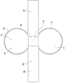
(第5実施形態)
図15、16に示すように、本実施形態の電子部品モジュール1は、平面形状が円形状である点が、第1実施形態の電子部品モジュール1と異なる。その他の構成は、第1実施形態の電子部品モジュール1と同じである。なお、図15、16では、複数の電子部品の図示を省略している。
(Fifth embodiment)
As shown in FIGS. 15 and 16, the
図16に示すように、プリント配線基板10の第1基板部11と第2基板部12の平面形状が円形状である。放熱板30の第1固定部31と第2固定部32の平面形状も円形状である。放熱板30は、側方部37、38を有している。
As shown in FIG. 16, the planar shape of the
図15、16に示すように、本実施形態の放熱板30は、第3固定部33と側方部37、38が折り曲げられて円柱形状とされる。第1基板部11と第2基板部12が、円柱の底面となる。側方部37、38が円柱の側面となる。本実施形態においても、側方部37、38が第1基板部11と第2基板部12の間の領域の周囲に位置する。このため、第1実施形態と同様の効果が得られる。
As shown in FIGS. 15 and 16, the
(他の実施形態)
本発明は上記した実施形態に限定されるものではなく、下記のように、特許請求の範囲に記載した範囲内において適宜変更が可能である。
(Other embodiments)
The present invention is not limited to the above-described embodiment, and can be appropriately modified within the scope described in the claims as follows.
(1)第1〜第3実施形態では、第1側方部34、第2側方部35および第3側方部36のそれぞれが、第1固定部31に連なっていたが、第1固定部31ではなく、第2固定部32に連なっていてもよい。また、第1側方部34、第2側方部35および第3側方部36のそれぞれが、第1固定部31と第2固定部32の一方のみに連なる場合に限定されない。第1側方部34、第2側方部35および第3側方部36のそれぞれが、第1固定部31と第2固定部32の両方に連なっていてもよい。この場合、例えば、第1側方部34は、第1固定部31に連なる部分と第2固定部32に連なる部分に分割される。
(1) In the first to third embodiments, each of the
(2)上記各実施形態では、放熱板30の側方部34、35、36は、側方部の全域において金属面が露出していたが、これに限定されない。側方部34、35、36は、絶縁が必要な箇所などの一部において、金属面が樹脂などの絶縁層で覆われていてもよい。
(2) In each of the embodiments described above, the metal surfaces of the
(3)上記各実施形態では、第3基板部13の一部131、132が屈曲した形状であったが、これに限定されない。第3基板部13の全部が屈曲した形状であってもよい。
(3) In the above embodiments, the
(4)上記各実施形態では、放熱板30は、プリント配線基板10の表面に固定されていたが、これに限定されない。放熱板30は、プリント配線基板10の内部に固定されていてもよい。すなわち、放熱板30は、プリント配線基板10を構成する絶縁基材101と絶縁基材101に挟まれた状態で、プリント配線基板10と接合されていてもよい。
(4) In each of the embodiments described above, the
(5)上記各実施形態は、互いに無関係なものではなく、組み合わせが明らかに不可な場合を除き、適宜組み合わせが可能である。また、上記各実施形態において、実施形態を構成する要素は、特に必須であると明示した場合および原理的に明らかに必須であると考えられる場合等を除き、必ずしも必須のものではないことは言うまでもない。
(まとめ)
上記各実施形態の一部または全部で示された第1の観点によれば、電子部品モジュールは、基板と、複数の電子部品と、放熱板とを備える。基板は、第1基板部と、第2基板部と、第3基板部とを有する。第1基板部と第2基板部は、第1基板部の一面と第2基板部の一面とを向かい合わせにして配置されている。第1基板部と第3基板部と第2基板部とが連なっている。放熱板は、第1基板部、第2基板部、第3基板部の少なくとも1つ以上に固定された固定部と、第1基板部と第2基板部に挟まれた領域の側方に位置する側方部とを有する。側方部は、屈曲した形状の屈曲部を介して、固定部と連なっている。
(5) The above-described embodiments are not irrelevant to each other, and can be appropriately combined unless the combination is clearly impossible. In each of the above-described embodiments, it is needless to say that elements constituting the embodiment are not necessarily essential unless explicitly stated as essential and clearly considered essential in principle. Yes.
(Summary)
According to the 1st viewpoint shown by one part or all part of said each embodiment, an electronic component module is provided with a board | substrate, a some electronic component, and a heat sink. The substrate includes a first substrate unit, a second substrate unit, and a third substrate unit. The first substrate portion and the second substrate portion are arranged with one surface of the first substrate portion facing one surface of the second substrate portion. The first substrate unit, the third substrate unit, and the second substrate unit are connected. The heat radiating plate is located on a side of a fixed portion fixed to at least one of the first substrate portion, the second substrate portion, and the third substrate portion, and a region sandwiched between the first substrate portion and the second substrate portion. Side portions to be The side portion is connected to the fixed portion via a bent portion having a bent shape.
また、第2の観点によれば、側方部は、第1部品と第2部品のうちの少なくとも1つ以上の電子部品に対して、接触している。これにより、電子部品の放熱性をより向上させることができる。 According to the second aspect, the side portion is in contact with at least one electronic component of the first component and the second component. Thereby, the heat dissipation of an electronic component can be improved more.
また、第3の観点によれば、放熱板は、グランド電位とされている。これにより、放熱板を電磁波シールドとして機能させることができる。すなわち、放熱板によって外部から複数の電子部品に向かう電磁波を遮断することができる。 Moreover, according to the 3rd viewpoint, the heat sink is made into ground potential. Thereby, a heat sink can be functioned as an electromagnetic wave shield. That is, it is possible to block electromagnetic waves traveling from the outside to the plurality of electronic components by the heat sink.
また、第4の観点によれば、固定部は、第1基板部、第2基板部および第3基板部のそれぞれに固定されている。側方部は、第1基板部と第2基板部に挟まれた領域の側方における第3基板部を除く全域に配置されている。これにより、放熱性をより向上させることができる。 Moreover, according to the 4th viewpoint, the fixing | fixed part is being fixed to each of a 1st board | substrate part, a 2nd board | substrate part, and a 3rd board | substrate part. The side portion is disposed in the entire area excluding the third substrate portion on the side of the region sandwiched between the first substrate portion and the second substrate portion. Thereby, heat dissipation can be improved more.
また、第5の観点によれば、電子部品モジュールの製造方法は、放熱板が固定された基板を準備することと、基板の表面に複数の電子部品を実装することと、実装された基板および放熱板のそれぞれを折り曲げることとを備える。折り曲げることは、基板を折り曲げて、第1基板部の一面と第2基板部の一面とを向かい合わせに配置するとともに、第1基板部と第2基板部の間を連ねる第3基板部を構成することを含む。折り曲げることは、さらに、側方部を折り曲げて、第1基板部と第2基板部に挟まれた領域の側方に側方部を位置させることとを含む。 According to a fifth aspect, the electronic component module manufacturing method includes preparing a substrate on which the heat sink is fixed, mounting a plurality of electronic components on the surface of the substrate, Folding each of the heat sinks. Bending means that the substrate is bent so that one surface of the first substrate portion and one surface of the second substrate portion face each other, and the third substrate portion that connects between the first substrate portion and the second substrate portion is formed. Including doing. Bending further includes bending the side portion and positioning the side portion to the side of the region sandwiched between the first substrate portion and the second substrate portion.
また、第6の観点によれば、領域の側方に側方部を位置させることでは、第1部品と第2部品のうちの少なくとも1つ以上の電子部品に対して、側方部を接触させる。これにより、電子部品の放熱性をより向上させることができる。 Further, according to the sixth aspect, by positioning the side portion on the side of the region, the side portion is brought into contact with at least one electronic component of the first component and the second component. Let Thereby, the heat dissipation of an electronic component can be improved more.
また、第7の観点によれば、放熱板が固定された基板を準備することでは、放熱板が基板のグランド電極と電気的に接続されたものを準備する。これにより、外部から複数の電子部品に向かう電磁波を遮断することができる。すなわち、放熱板を電磁波シールドとして機能させることができる。 According to the seventh aspect, by preparing a substrate to which the heat sink is fixed, a substrate in which the heat sink is electrically connected to the ground electrode of the substrate is prepared. Thereby, the electromagnetic wave which goes to a some electronic component from the outside can be interrupted | blocked. That is, the heat sink can function as an electromagnetic wave shield.
また、第8の観点によれば、放熱板が固定された基板を準備することでは、固定部が第1基板部、第2基板部、第3基板部のそれぞれに重なって固定されたものを準備する。領域の側方に側方部を位置させることでは、側方部を、領域の側方における第3基板部を除く全域に位置させる。これにより、電子部品の放熱性をより向上させることができる。 Further, according to the eighth aspect, in preparing the substrate on which the heat sink is fixed, the fixing portion is overlapped and fixed on each of the first substrate portion, the second substrate portion, and the third substrate portion. prepare. By positioning the side portion on the side of the region, the side portion is positioned on the entire region excluding the third substrate portion on the side of the region. Thereby, the heat dissipation of an electronic component can be improved more.
10 プリント配線基板
11 第1基板部
12 第2基板部
13 第3基板部
30 放熱板
31 第1固定部
32 第2固定部
33 第3固定部
34 第1側方部
35 第2側方部
36 第3側方部
DESCRIPTION OF
Claims (8)
基板(10)と、
前記基板の表面(11a、12a)に実装された複数の電子部品(21、22)と、
前記基板に固定され、金属で構成された放熱板(30)とを備え、
前記基板は、第1基板部(11)と、第2基板部(12)と、第3基板部(13)とを有し、
前記複数の電子部品は、前記第1基板部の一面(11a)に実装された1つ以上の第1部品(21)と、前記第2基板部の一面(12a)に実装された1つ以上の第2部品(22)とを有し、
前記第1基板部と前記第2基板部は、前記第1基板部の前記一面と前記第2基板部の前記一面とを向かい合わせにして配置されており、
前記第3基板部が前記第1基板部と前記第2基板部の間に配置されることにより、前記第1基板部と、前記第3基板部と、前記第2基板部とが連なっており、
前記放熱板は、前記第1基板部、前記第2基板部、前記第3基板部の少なくとも1つ以上に固定された固定部(31、32、33)と、前記第1基板部と前記第2基板部に挟まれた領域(R1)の側方に位置する側方部(34、35、36)とを有し、
前記側方部は、屈曲した形状の屈曲部を介して、前記固定部と連なっている電子部品モジュール。 An electronic component module in which a plurality of electronic components are integrated,
A substrate (10);
A plurality of electronic components (21, 22) mounted on the surface (11a, 12a) of the substrate;
A heat sink (30) fixed to the substrate and made of metal,
The substrate has a first substrate portion (11), a second substrate portion (12), and a third substrate portion (13),
The plurality of electronic components include one or more first components (21) mounted on one surface (11a) of the first substrate unit and one or more mounted on one surface (12a) of the second substrate unit. A second part (22) of
The first substrate portion and the second substrate portion are arranged with the one surface of the first substrate portion facing the one surface of the second substrate portion,
Since the third substrate unit is disposed between the first substrate unit and the second substrate unit, the first substrate unit, the third substrate unit, and the second substrate unit are connected. ,
The heat sink includes a fixed portion (31, 32, 33) fixed to at least one of the first substrate portion, the second substrate portion, and the third substrate portion, the first substrate portion, and the first substrate portion. 2 side portions (34, 35, 36) located on the sides of the region (R1) sandwiched between the two substrate portions,
The side part is an electronic component module connected to the fixed part via a bent part having a bent shape.
前記側方部は、前記領域の側方における前記第3基板部を除く全域に配置されている請求項1ないし3のいずれか1つに記載の電子部品モジュール。 The fixing portion is fixed to each of the first substrate portion, the second substrate portion, and the third substrate portion,
4. The electronic component module according to claim 1, wherein the side portion is disposed in an entire region excluding the third substrate portion on a side of the region. 5.
放熱板(30)が固定された基板(10)を準備することと、
前記基板の表面(11a、12a)に複数の電子部品(21、22)を実装することと、
実装された前記基板および前記放熱板のそれぞれを折り曲げることとを備え、
準備される前記基板は、第1基板部(11)と、第2基板部(12)と、前記第1基板部と前記第2基板部の両方に連なる第3基板部(13)とを有し、
前記基板に固定された前記放熱板は、前記第1基板部、前記第2基板部、前記第3基板部の少なくとも1つ以上に重なって固定された固定部(31、32、33)と、前記固定部に連なっており、前記第1基板部、前記第2基板部、前記第3基板部のいずれとも重なっていない側方部(34、35、36)とを有し、
前記実装することは、前記第1基板部の一面(11a)に1つ以上の第1部品(21)を実装することと、前記第2基板部の一面(12a)に1つ以上の第2部品(22)を実装することとを含み、
前記折り曲げることは、前記基板を折り曲げて、前記第1基板部の前記一面と前記第2基板部の前記一面とを向かい合わせに配置するとともに、前記第1基板部と前記第2基板部の間を連ねる前記第3基板部を構成することと、前記側方部を折り曲げて、前記第1基板部と前記第2基板部に挟まれた領域(R1)の側方に前記側方部を位置させることとを含む電子部品モジュールの製造方法。 A method of manufacturing an electronic component module in which a plurality of electronic components are integrated,
Preparing a substrate (10) to which a heat sink (30) is fixed;
Mounting a plurality of electronic components (21, 22) on the surface (11a, 12a) of the substrate;
Bending each of the mounted substrate and the heat sink,
The prepared substrate includes a first substrate unit (11), a second substrate unit (12), and a third substrate unit (13) connected to both the first substrate unit and the second substrate unit. And
The heat radiating plate fixed to the substrate includes fixed portions (31, 32, 33) fixed to overlap at least one of the first substrate portion, the second substrate portion, and the third substrate portion, A side portion (34, 35, 36) that is connected to the fixed portion and does not overlap any of the first substrate portion, the second substrate portion, and the third substrate portion;
The mounting includes mounting one or more first components (21) on one surface (11a) of the first substrate portion and one or more second components on one surface (12a) of the second substrate portion. Mounting the component (22),
The bending includes bending the substrate to arrange the one surface of the first substrate portion and the one surface of the second substrate portion facing each other, and between the first substrate portion and the second substrate portion. And the side part is located on the side of the region (R1) sandwiched between the first and second substrate parts by bending the side part. Manufacturing the electronic component module.
前記領域の側方に前記側方部を位置させることでは、前記側方部を、前記領域の側方における前記第3基板部を除く全域に位置させる請求項5ないし7のいずれか1つに記載の電子部品モジュールの製造方法。 In preparing the substrate to which the heat sink is fixed, the fixing portion is prepared by overlapping and fixing each of the first substrate portion, the second substrate portion, and the third substrate portion,
The positioning of the side portion on a side of the region causes the side portion to be positioned on the entire region excluding the third substrate portion on the side of the region. The manufacturing method of the electronic component module of description.
Priority Applications (6)
| Application Number | Priority Date | Filing Date | Title |
|---|---|---|---|
| JP2015235905A JP2017103366A (en) | 2015-12-02 | 2015-12-02 | Electronic component module and manufacturing method therefor |
| US15/780,728 US20200258805A1 (en) | 2015-12-02 | 2016-12-01 | Electronic component module provided with substrate on which electronic components are mounted and heat sink and manufacturing method of the same |
| KR1020187016114A KR20180081767A (en) | 2015-12-02 | 2016-12-01 | Electronic component module having a substrate on which electronic components are mounted, a heat sink, and a manufacturing method thereof |
| CN201680071521.3A CN108370642A (en) | 2015-12-02 | 2016-12-01 | Have the electronic component module and its manufacturing method of the substrate and heat sink of installation electronic unit |
| PCT/JP2016/085719 WO2017094834A1 (en) | 2015-12-02 | 2016-12-01 | Electronic component module equipped with heat sink and substrate having electronic components mounted thereon, and method for producing same |
| TW105139926A TW201733414A (en) | 2015-12-02 | 2016-12-02 | Electronic component module equipped with heat sink and substrate having electronic components mounted thereon, and method for producing same |
Applications Claiming Priority (1)
| Application Number | Priority Date | Filing Date | Title |
|---|---|---|---|
| JP2015235905A JP2017103366A (en) | 2015-12-02 | 2015-12-02 | Electronic component module and manufacturing method therefor |
Publications (2)
| Publication Number | Publication Date |
|---|---|
| JP2017103366A true JP2017103366A (en) | 2017-06-08 |
| JP2017103366A5 JP2017103366A5 (en) | 2018-01-18 |
Family
ID=58796963
Family Applications (1)
| Application Number | Title | Priority Date | Filing Date |
|---|---|---|---|
| JP2015235905A Pending JP2017103366A (en) | 2015-12-02 | 2015-12-02 | Electronic component module and manufacturing method therefor |
Country Status (6)
| Country | Link |
|---|---|
| US (1) | US20200258805A1 (en) |
| JP (1) | JP2017103366A (en) |
| KR (1) | KR20180081767A (en) |
| CN (1) | CN108370642A (en) |
| TW (1) | TW201733414A (en) |
| WO (1) | WO2017094834A1 (en) |
Cited By (1)
| Publication number | Priority date | Publication date | Assignee | Title |
|---|---|---|---|---|
| WO2022195865A1 (en) * | 2021-03-19 | 2022-09-22 | サンケン電気株式会社 | Four-sided cooling power module |
Families Citing this family (1)
| Publication number | Priority date | Publication date | Assignee | Title |
|---|---|---|---|---|
| US11456231B2 (en) * | 2021-01-18 | 2022-09-27 | Fortinet, Inc. | Heatsink arrangement for integrated circuit assembly and method for assembling thereof |
Citations (4)
| Publication number | Priority date | Publication date | Assignee | Title |
|---|---|---|---|---|
| US5265322A (en) * | 1990-02-05 | 1993-11-30 | Motorola, Inc. | Electronic module assembly and method of forming same |
| US5925298A (en) * | 1995-06-26 | 1999-07-20 | Ford Motor Company | Method for reworking a multi-layer circuit board using a shape memory alloy material |
| JP2000183574A (en) * | 1998-12-15 | 2000-06-30 | Tdk Corp | Electronic apparatus |
| JP2013012508A (en) * | 2011-06-28 | 2013-01-17 | Ntt Electornics Corp | Electronic apparatus |
Family Cites Families (6)
| Publication number | Priority date | Publication date | Assignee | Title |
|---|---|---|---|---|
| JPS62118492U (en) * | 1986-01-20 | 1987-07-28 | ||
| JP2006100302A (en) * | 2004-09-28 | 2006-04-13 | Sharp Corp | Radio frequency module and manufacturing method therefor |
| JP4697037B2 (en) | 2006-05-09 | 2011-06-08 | 株式会社デンソー | Component built-in board and wiring defect inspection method thereof |
| DE102009060777A1 (en) * | 2009-12-22 | 2011-06-30 | Automotive Lighting Reutlingen GmbH, 72762 | Electronic control unit and method for producing a unit from a base body and a printed circuit board for use in such a control unit |
| CN201869439U (en) * | 2010-12-05 | 2011-06-15 | 新高电子材料(中山)有限公司 | Metal-based circuit board with high heat radiation |
| CN204560003U (en) * | 2015-02-09 | 2015-08-12 | 江阴通利光电科技有限公司 | A kind of flexible circuit board component |
-
2015
- 2015-12-02 JP JP2015235905A patent/JP2017103366A/en active Pending
-
2016
- 2016-12-01 WO PCT/JP2016/085719 patent/WO2017094834A1/en active Application Filing
- 2016-12-01 CN CN201680071521.3A patent/CN108370642A/en not_active Withdrawn
- 2016-12-01 US US15/780,728 patent/US20200258805A1/en not_active Abandoned
- 2016-12-01 KR KR1020187016114A patent/KR20180081767A/en active Search and Examination
- 2016-12-02 TW TW105139926A patent/TW201733414A/en unknown
Patent Citations (4)
| Publication number | Priority date | Publication date | Assignee | Title |
|---|---|---|---|---|
| US5265322A (en) * | 1990-02-05 | 1993-11-30 | Motorola, Inc. | Electronic module assembly and method of forming same |
| US5925298A (en) * | 1995-06-26 | 1999-07-20 | Ford Motor Company | Method for reworking a multi-layer circuit board using a shape memory alloy material |
| JP2000183574A (en) * | 1998-12-15 | 2000-06-30 | Tdk Corp | Electronic apparatus |
| JP2013012508A (en) * | 2011-06-28 | 2013-01-17 | Ntt Electornics Corp | Electronic apparatus |
Cited By (1)
| Publication number | Priority date | Publication date | Assignee | Title |
|---|---|---|---|---|
| WO2022195865A1 (en) * | 2021-03-19 | 2022-09-22 | サンケン電気株式会社 | Four-sided cooling power module |
Also Published As
| Publication number | Publication date |
|---|---|
| WO2017094834A1 (en) | 2017-06-08 |
| US20200258805A1 (en) | 2020-08-13 |
| TW201733414A (en) | 2017-09-16 |
| KR20180081767A (en) | 2018-07-17 |
| CN108370642A (en) | 2018-08-03 |
Similar Documents
| Publication | Publication Date | Title |
|---|---|---|
| JP2017201732A (en) | Circuit board and method of manufacturing the same | |
| JPWO2019167908A1 (en) | High frequency module | |
| JP2004128418A (en) | Semiconductor device and manufacturing method thereof | |
| WO2008059643A1 (en) | Three-dimensional electronic circuit apparatus | |
| US20080066953A1 (en) | Circuit board assembly and manufacturing method thereof, electronic part assembly and manufacturing method thereof, and electronic device | |
| JP6160308B2 (en) | Laminated board | |
| WO2017094834A1 (en) | Electronic component module equipped with heat sink and substrate having electronic components mounted thereon, and method for producing same | |
| JP6093093B2 (en) | Semiconductor module | |
| JP5692473B1 (en) | Component built-in board and communication module | |
| JP2015138925A (en) | Multilayer wiring board | |
| JP2014045042A (en) | Mounting structure and electronic apparatus | |
| JP2009239109A (en) | Electronic component wiring board, and component mounting module | |
| CN111052880A (en) | Circuit board and method for manufacturing the same | |
| KR101288211B1 (en) | Method for manufacturing electric device module | |
| JP2009117409A (en) | Circuit board | |
| KR20150079189A (en) | Electronic components embedded substrate | |
| JP2012146823A (en) | Shield method and electronic apparatus | |
| JP2006202870A (en) | Three-dimensional electronic circuit module, its manufacturing method, and electronic apparatus using them | |
| JPWO2015118951A1 (en) | Resin multilayer board and component module | |
| JP2007324246A (en) | Semiconductor device and manufacturing method thereof | |
| KR101485058B1 (en) | Loop antenna and manufacturing method of the same | |
| JP2014078578A (en) | Electronic component module | |
| JP2009123781A (en) | Circuit module | |
| JP2018137343A (en) | Printed circuit board and inverter | |
| JP2009231480A (en) | Semiconductor device |
Legal Events
| Date | Code | Title | Description |
|---|---|---|---|
| A521 | Request for written amendment filed |
Free format text: JAPANESE INTERMEDIATE CODE: A523 Effective date: 20171127 |
|
| A621 | Written request for application examination |
Free format text: JAPANESE INTERMEDIATE CODE: A621 Effective date: 20171127 |
|
| A131 | Notification of reasons for refusal |
Free format text: JAPANESE INTERMEDIATE CODE: A131 Effective date: 20190115 |
|
| A02 | Decision of refusal |
Free format text: JAPANESE INTERMEDIATE CODE: A02 Effective date: 20190709 |