JP2017069998A - Piezoelectric drive device, manufacturing method for the same, motor, robot and pump - Google Patents
Piezoelectric drive device, manufacturing method for the same, motor, robot and pump Download PDFInfo
- Publication number
- JP2017069998A JP2017069998A JP2015189395A JP2015189395A JP2017069998A JP 2017069998 A JP2017069998 A JP 2017069998A JP 2015189395 A JP2015189395 A JP 2015189395A JP 2015189395 A JP2015189395 A JP 2015189395A JP 2017069998 A JP2017069998 A JP 2017069998A
- Authority
- JP
- Japan
- Prior art keywords
- piezoelectric
- silicon substrate
- longitudinal direction
- electrode
- driving device
- Prior art date
- Legal status (The legal status is an assumption and is not a legal conclusion. Google has not performed a legal analysis and makes no representation as to the accuracy of the status listed.)
- Withdrawn
Links
Images


Abstract
Description
本発明は、圧電駆動装置およびその製造方法、モーター、ロボット、ならびにポンプに関する。 The present invention relates to a piezoelectric drive device and a manufacturing method thereof, a motor, a robot, and a pump.
圧電体を振動させて被駆動体を駆動する圧電アクチュエーター(圧電駆動装置)は、磁石やコイルが不要のため、様々な分野で利用されている(例えば特許文献1参照)。このような圧電駆動装置には、一般的に、バルク状の圧電体を備えた圧電素子(バルク圧電素子)が利用されている(例えば特許文献2参照)。 A piezoelectric actuator (piezoelectric drive device) that drives a driven body by vibrating a piezoelectric body is used in various fields because a magnet and a coil are not required (see, for example, Patent Document 1). In general, such a piezoelectric drive device uses a piezoelectric element (bulk piezoelectric element) including a bulk piezoelectric body (see, for example, Patent Document 2).
一方、圧電素子としては、薄膜状の圧電体を備えたもの(薄膜圧電素子)が知られている。薄膜圧電素子は、主に、インクジェットプリンターのヘッドにおいて、インクの射出を行うために利用されている。 On the other hand, as a piezoelectric element, a thin film piezoelectric element (thin film piezoelectric element) is known. Thin film piezoelectric elements are mainly used for ejecting ink in the heads of ink jet printers.
上記のような薄膜圧電素子を圧電駆動装置に用いれば、圧電駆動装置やこれによって駆動される機器を小型化することができる。しかしながら、このような薄膜圧電素子を用いた圧電駆動装置では、小型であるがために、出力が不足する場合がある。 If the thin film piezoelectric element as described above is used in a piezoelectric driving device, the piezoelectric driving device and the device driven by the piezoelectric driving device can be reduced in size. However, the piezoelectric drive device using such a thin film piezoelectric element is small in size, and therefore, the output may be insufficient.
本発明のいくつかの態様に係る目的の1つは、高出力化を図ることができる圧電駆動装置を提供することにある。また本発明のいくつかの態様に係る目的の1つは、高出力化を図ることができる圧電駆動装置の製造方法を提供することにある。また、本発明のいくつかの態様に係る目的の1つは、上記の圧電駆動装置を含むモーター、ロボット、およびポンプを提供することにある。 One of the objects according to some aspects of the present invention is to provide a piezoelectric driving device capable of achieving high output. Another object of some aspects of the present invention is to provide a method of manufacturing a piezoelectric driving device capable of achieving high output. Another object of some embodiments of the present invention is to provide a motor, a robot, and a pump including the above-described piezoelectric driving device.
本発明は上述の課題の少なくとも一部を解決するためになされたものであり、以下の態様又は適用例として実現することができる。 SUMMARY An advantage of some aspects of the invention is to solve at least a part of the problems described above, and the invention can be implemented as the following aspects or application examples.
[適用例1]
本発明に係る圧電駆動装置の一態様は、
長手方向と、前記長手方向と直交する短手方向と、を有するシリコン基板と、
前記シリコン基板上に設けられ、第1電極と、第2電極と、前記第1電極と前記第2電極との間に位置する圧電体と、を有する圧電素子と、
前記長手方向の先端部に設けられ、被駆動体に接触する突起部と、
を含み、
前記シリコン基板の前記短手方向のヤング率は、前記シリコン基板の前記長手方向のヤング率よりも小さい。
[Application Example 1]
One aspect of the piezoelectric drive device according to the present invention is:
A silicon substrate having a longitudinal direction and a transverse direction orthogonal to the longitudinal direction;
A piezoelectric element provided on the silicon substrate and having a first electrode, a second electrode, and a piezoelectric body positioned between the first electrode and the second electrode;
A protrusion provided at the distal end in the longitudinal direction and in contact with the driven body;
Including
The Young's modulus in the short direction of the silicon substrate is smaller than the Young's modulus in the longitudinal direction of the silicon substrate.
このような圧電駆動装置では、シリコン基板のヤング率が小さい方向を、長手方向ではなく短手方向にすることによって、シリコン基板の短手方向に沿った屈曲振動の振幅を大
きくすることができ、高出力化を図ることができる。
In such a piezoelectric driving device, the amplitude of the bending vibration along the short direction of the silicon substrate can be increased by setting the direction in which the Young's modulus of the silicon substrate is small to the short direction instead of the long direction, High output can be achieved.
[適用例2]
適用例1において、
前記シリコン基板は、{110}基板であってもよい。
[Application Example 2]
In application example 1,
The silicon substrate may be a {110} substrate.
このような圧電駆動装置では、シリコン基板の面内において直交する2方向のヤング率を、異ならせることができる。 In such a piezoelectric driving device, the Young's modulus in two directions orthogonal to each other in the plane of the silicon substrate can be made different.
[適用例3]
適用例2において、
前記シリコン基板の前記長手方向は、<110>方向であり、
前記シリコン基板の前記短手方向は、<100>方向であってもよい。
[Application Example 3]
In application example 2,
The longitudinal direction of the silicon substrate is a <110> direction,
The short side direction of the silicon substrate may be a <100> direction.
このような圧電駆動装置では、高出力化を図ることができる。 In such a piezoelectric drive device, high output can be achieved.
[適用例4]
適用例2において、
前記シリコン基板の前記長手方向は、<111>方向であり、
前記シリコン基板の前記短手方向は、<112>方向であってもよい。
[Application Example 4]
In application example 2,
The longitudinal direction of the silicon substrate is a <111> direction,
The short side direction of the silicon substrate may be a <112> direction.
このような圧電駆動装置では、高出力化を図ることができる。 In such a piezoelectric drive device, high output can be achieved.
[適用例5]
適用例1ないし4のいずれか1例において、
前記圧電体の厚さは、50nm以上20μm以下であってもよい。
[Application Example 5]
In any one of Application Examples 1 to 4,
The piezoelectric body may have a thickness of 50 nm to 20 μm.
このような圧電駆動装置では、圧電体の絶縁破壊を防ぎつつ、高出力化を図ることができる。 In such a piezoelectric drive device, high output can be achieved while preventing dielectric breakdown of the piezoelectric body.
[適用例6]
本発明に係る圧電駆動装置の製造方法の一態様は、
面内において直交する2方向のヤング率が互いに異なるシリコンウェハーを準備する工程と、
前記シリコンウェハー上に、第1電極と、第2電極と、前記第1電極と前記第2電極との間に位置する圧電体と、を有する圧電素子を形成する工程と、
前記シリコンウェハーを加工して、長手方向と前記長手方向と直交する短手方向とを有するシリコン基板と、前記シリコン基板上に形成された前記圧電素子と、を有するチップを取り出す工程と、
前記チップの前記長手方向の先端部に、被駆動体に接触する突起部を取り付ける工程と、
を含み、
前記シリコン基板の前記短手方向のヤング率が、前記シリコン基板の前記長手方向のヤング率よりも小さくなるように、前記シリコンウェハー内に前記チップを配列する。
[Application Example 6]
One aspect of a method for manufacturing a piezoelectric drive device according to the present invention is as follows.
Preparing silicon wafers having different Young's moduli in two directions perpendicular to each other in a plane;
Forming a piezoelectric element having a first electrode, a second electrode, and a piezoelectric body located between the first electrode and the second electrode on the silicon wafer;
Processing the silicon wafer to take out a chip having a silicon substrate having a longitudinal direction and a transverse direction orthogonal to the longitudinal direction, and the piezoelectric element formed on the silicon substrate;
Attaching a protrusion contacting the driven body to the tip in the longitudinal direction of the chip;
Including
The chips are arranged in the silicon wafer such that the Young's modulus in the short direction of the silicon substrate is smaller than the Young's modulus in the longitudinal direction of the silicon substrate.
このような圧電駆動装置の製造方法では、高出力化を図ることができる圧電駆動装置を製造することができる。 In such a method for manufacturing a piezoelectric driving device, a piezoelectric driving device capable of achieving high output can be manufactured.
[適用例7]
適用例6において、
前記シリコン基板は、{110}基板であってもよい。
[Application Example 7]
In Application Example 6,
The silicon substrate may be a {110} substrate.
このような圧電駆動装置の製造方法では、シリコン基板の面内において直交する2方向のヤング率を、異ならせることができる。 In such a method for manufacturing a piezoelectric driving device, the Young's moduli in two directions orthogonal to each other in the plane of the silicon substrate can be made different.
[適用例8]
適用例7において、
前記シリコン基板の前記長手方向は、<110>方向であり、
前記シリコン基板の前記短手方向は、<100>方向であってもよい。
[Application Example 8]
In Application Example 7,
The longitudinal direction of the silicon substrate is a <110> direction,
The short side direction of the silicon substrate may be a <100> direction.
このような圧電駆動装置の製造方法では、高出力化を図ることができる圧電駆動装置を製造することができる。 In such a method for manufacturing a piezoelectric driving device, a piezoelectric driving device capable of achieving high output can be manufactured.
[適用例9]
適用例7において、
前記シリコン基板の前記長手方向は、<111>方向であり、
前記シリコン基板の前記短手方向は、<112>方向であってもよい。
[Application Example 9]
In Application Example 7,
The longitudinal direction of the silicon substrate is a <111> direction,
The short side direction of the silicon substrate may be a <112> direction.
このような圧電駆動装置の製造方法では、高出力化を図ることができる圧電駆動装置を製造することができる。 In such a method for manufacturing a piezoelectric driving device, a piezoelectric driving device capable of achieving high output can be manufactured.
[適用例10]
適用例6ないし9のいずれか1例において、
前記圧電体の厚さは、50nm以上20μm以下であってもよい。
[Application Example 10]
In any one of Application Examples 6 to 9,
The piezoelectric body may have a thickness of 50 nm to 20 μm.
このような圧電駆動装置の製造方法では、圧電体にクラックが発生することを抑制しつつ、高出力化を図ることができる圧電駆動装置を製造することができる。 With such a method for manufacturing a piezoelectric drive device, it is possible to manufacture a piezoelectric drive device that can achieve high output while suppressing the occurrence of cracks in the piezoelectric body.
[適用例11]
本発明に係るモーターの一態様は、
適用例1ないし5のいずれか1例に記載の圧電駆動装置と、
前記圧電駆動装置によって回転されるローターと、
を含む。
[Application Example 11]
One aspect of the motor according to the present invention is:
The piezoelectric drive device according to any one of Application Examples 1 to 5, and
A rotor rotated by the piezoelectric drive device;
including.
このようなモーターは、本発明に係る圧電駆動装置を含むため、高出力化を図ることができる。 Since such a motor includes the piezoelectric drive device according to the present invention, high output can be achieved.
[適用例12]
本発明に係るロボットの一態様は、
複数のリンク部と、
複数の前記リンク部を接続する関節部と、
複数の前記リンク部を前記関節部で回動させる適用例1ないし5のいずれか1例に記載の圧電駆動装置と、
を含む。
[Application Example 12]
One aspect of the robot according to the present invention is:
A plurality of link parts;
A joint part connecting a plurality of the link parts;
The piezoelectric drive device according to any one of Application Examples 1 to 5 in which a plurality of the link portions are rotated by the joint portions;
including.
このようなロボットでは、本発明に係る圧電駆動装置を含むことができる。 Such a robot can include the piezoelectric driving device according to the present invention.
[適用例13]
本発明に係るロボットの一態様は、
適用例1ないし5のいずれか1例に記載の圧電駆動装置と、
液体を輸送するチューブと、
前記圧電駆動装置の駆動によって前記チューブを閉鎖する複数のフィンガーと、
を含む。
[Application Example 13]
One aspect of the robot according to the present invention is:
The piezoelectric drive device according to any one of Application Examples 1 to 5, and
A tube that transports the liquid;
A plurality of fingers for closing the tube by driving the piezoelectric driving device;
including.
このようなポンプでは、本発明に係る圧電駆動装置を含むことができる。 Such a pump can include a piezoelectric drive according to the present invention.
以下、本発明の好適な実施形態について、図面を用いて詳細に説明する。なお、以下に説明する実施形態は、特許請求の範囲に記載された本発明の内容を不当に限定するものではない。また、以下で説明される構成の全てが本発明の必須構成要件であるとは限らない。 DESCRIPTION OF EMBODIMENTS Hereinafter, preferred embodiments of the present invention will be described in detail with reference to the drawings. The embodiments described below do not unduly limit the contents of the present invention described in the claims. In addition, not all of the configurations described below are essential constituent requirements of the present invention.
1. 圧電駆動装置
まず、本実施形態に係る圧電駆動装置について、図面を参照しながら説明する。図1は、本実施形態に係る圧電駆動装置100を模式的に示す平面図である。図2は、本実施形態に係る圧電駆動装置100を模式的に示す図1のII−II線断面図である。図3は、本実施形態に係る圧電駆動装置100を模式的に示す平面図である。
1. Piezoelectric Drive Device First, a piezoelectric drive device according to the present embodiment will be described with reference to the drawings. FIG. 1 is a plan view schematically showing a
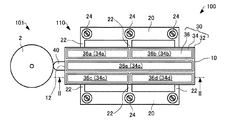
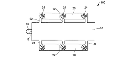
圧電駆動装置100は、図1〜図3に示すように、シリコン基板10と、取付部20と、圧電素子30と、突起部40と、を含む。圧電駆動装置100と、ローター(被駆動体)2とは、モーター101を構成している。ローター2は、圧電駆動装置100によって回転される。なお、便宜上、図3では、ローター2および圧電素子30の部材の図示を省略している。
As shown in FIGS. 1 to 3, the
シリコン基板10は、例えば、{110}基板である。シリコン基板10は、例えば、{110}面で切り出された基板である。ここで、{110}は、(110)と等価な面を表している。したがって、シリコン基板10は、例えば、(110)基板であってもよいし、(−110)基板であってもよいし、(−1−10)基板であってもよい。なお、本明細書において、単位格子の負の面方位または負の方向の「1bar」や「2bar」については、それぞれ「−1」、「−2」と表記している。
The
シリコン基板10は、図1および図3に示すように、長手方向と、長手方向と直交する短手方向と、を有する形状である。図示の例では、シリコン基板10の平面形状は、長方形である。長手方向は、長辺が延びる方向であり、短手方向は、短辺が延びる方向である。
As shown in FIGS. 1 and 3, the
取付部20は、図1および図3に示すように、例えば、平面視においてシリコン基板10の長辺からそれぞれ3本ずつ延びる接続部22を介して、シリコン基板10に設けられている。取付部20および接続部22の材質は、シリコン基板10と同じ材質であってもよい。取付部20および接続部22は、図3に示すように、シリコン基板10と一体的に設けられていてもよい。取付部20は、ネジ24によって他の部材に圧電駆動装置100を取り付けるために用いられる。
As shown in FIGS. 1 and 3, the
圧電素子30は、シリコン基板10上に設けられている。図示はしないが、圧電素子30は、例えば、圧電素子30とシリコン基板10との密着性を向上させる密着層などを介して、シリコン基板10上に形成されていてもよい。シリコン基板10、取付部20、接続部22、および圧電素子30は、チップ110を構成している。圧電素子30は、図2に示すように、第1電極32と、圧電体34と、第2電極36と、を有している。
The
第1電極32は、シリコン基板10上に設けられている。図1に示す例では、第1電極32の平面形状は、長方形である。第1電極32は、シリコン基板10上に設けられたイリジウム層と、イリジウム層上に設けられた白金層と、によって構成されていてもよい。イリジウム層の厚さは、例えば、5nm以上100nm以下である。白金層の厚さは、例えば、50nm以上300nm以下である。なお、第1電極32は、Ti、Pt、Ta、Ir、Sr、In、Sn、Au、Al、Fe、Cr、Ni、Cuなどからなる金属層、またはこれらの2種以上を混合または積層したものであってもよい。第1電極32は、圧電体34に電圧を印加するための一方の電極である。
The
圧電体34は、第1電極32上に設けられている。圧電体34は、第1電極32と第2電極36との間に位置する。圧電体34の厚さは、例えば、50nm以上20μm以下であり、好ましくは、1μm以上7μm以下である。このように、圧電素子30は、薄膜圧電素子である。圧電体34の厚さが50nmより小さいと、圧電駆動装置100の出力が小さくなる場合がある。具体的には、出力を上げようとして圧電体34への印加電圧を高くすると、圧電体34が絶縁破壊を起こす場合がある。圧電体34の厚さが20μmより大きいと、圧電体34にクラックが生じる場合がある。
The
圧電体34としては、ペロブスカイト型酸化物の圧電材料を用いる。具体的には、圧電体34の材質は、例えば、チタン酸ジルコン酸鉛(Pb(Zr,Ti)O3:PZT)、ニオブ酸チタン酸ジルコン酸鉛(Pb(Zr,Ti,Nb)O3:PZTN)である。
As the
第2電極36は、圧電体34上に設けられている。第2電極36は、圧電体34上に設けられた密着層と、密着層上に設けられた導電層と、によって構成されていてもよい。密着層の厚さは、例えば、10nm以上100nm以下である。密着層は、例えば、TiW層、Ti層、Cr層、NiCr層や、これらの積層体である。導電層の厚さは、例えば、1μm以上10μm以下である。導電層は、例えば、Cu層、Au層、Al層やこれらの積層体である。第2電極36は、圧電体34に電圧を印加するための他方の電極である。
The
圧電素子30では、図1および図2に示すように、第1電極32は、1つの連続的な導電体層(第1電極層)として形成されている。一方、第2電極36は、5つの導電体層(第2電極層)36a,36b,36c,36d,36eに区分されている。同様に、圧電体34は、5つの圧電体層34a,34b,34c,34d,34eに区分されている。
図示の例では、圧電体層34a〜34dの面積は同じであり、圧電体層34eは、圧電体層34a〜34dよりも大きな面積を有している。圧電体層34a,34bは圧電体層の長手方向に並んで設けられ、圧電体層34c,34dは圧電体層の長手方向に並んで設けられ、圧電体層34a,34bと圧電体層34c,34との間に圧電体層34eが設けられている。第2電極層36a〜36eは、それぞれ圧電体層34a〜34e上に設けられている。図1に示す例では、圧電体層34a〜34eおよび第2電極層36a〜36eの平面形状は、矩形である。
In the
In the illustrated example, the
なお、図示はしないが、第2電極36が1つの連続的な導電層として形成されており、第1電極32が5つの導電体層に区分されていてもよい。また、図2に示す例では、シリコン基板10の一方の主面に圧電素子30が設けられているが、シリコン基板10の他方の主面(一方の主面と反対側の主面)にも圧電素子30が設けられていてもよい。
Although not shown, the
突起部40は、シリコン基板10の長手方向Aの先端部12に設けられている。図示の例では、突起部40は、シリコン基板10の長手方向Aの側面に設けられている。突起部40は、ローター2に接触し、シリコン基板10の動きをローター2に伝える部材である。突起部40は、接着剤(図示せず)を介してシリコン基板10に設けられていてもよい。突起部40の材質は、例えば、セラミックス(具体的にはアルミナ(Al2O3)、ジルコニア(ZrO2)、窒化ケイ素(Si3N)など)である。
The protruding
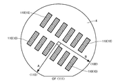
ここで、図4および図5は、シリコン基板10の長手方向Aおよび短手方向Bを説明するための平面図である。図4および図5に示すように、シリコンウェハー4上に多数のチップ110を配列することで、1枚のシリコンウェハー4から多数のチップ110を得ることができる。チップ110をどのような向きに配列するかは、シリコン基板10のヤング率を考慮して決定される。
4 and 5 are plan views for explaining the longitudinal direction A and the short direction B of the
なお、図4および図5において、「OF」は、オリフラ(オリエンテーション・フラット(orientation flat))を意味し、<111>方向に(例えば、シリコン基板10が(110)基板である場合には、[−111]方向に)位置している。
4 and 5, “OF” means an orientation flat (orientation flat), and in the <111> direction (for example, when the
図4に示すように、シリコン基板10の長手方向A(矢印Aの方向)は、<110>方向であり、シリコン基板10の短手方向B(矢印Bの方向)は、<100>方向であってもよい。ここで、<110>方向は、[110]方向と等価な方向を表しており、<100>方向は、[100]方向と等価な方向を表している。例えばシリコン基板10が(110)基板である場合、シリコン基板10の長手方向Aは、[−110]方向であり、シリコン基板10の短手方向Bは、[001]方向であってもよい。
As shown in FIG. 4, the longitudinal direction A (direction of arrow A) of the
または、図5に示すように、シリコン基板10の長手方向Aは、<111>方向であり、シリコン基板10の短手方向Bは、<112>方向であってもよい。ここで、<111>方向は、[111]方向と等価な方向を表しており、<112>方向は、[112]方向と等価な方向を表している。例えばシリコン基板10が(110)基板である場合、シリコン基板10の長手方向Aは、[−111]方向であり、シリコン基板10の短手方向Bは、[1−12]方向であってもよい。
Alternatively, as shown in FIG. 5, the longitudinal direction A of the
シリコン基板10では、面内において直交する2方向においてヤング率が異なる。シリコン基板10の短手方向Bのヤング率は、シリコン基板10の長手方向Aのヤング率よりも小さい。シリコン基板10は、圧電素子30の変形によって、変形することができる。
In the
ここで、図6は、圧電駆動装置100と駆動回路50との電気的接続状態を説明するための図である。図6に示すように、5つの第2電極層36a〜36eのうちで、対角にあ
る一対の第2電極層36a,36dは、配線60を介して互いに電気的に接続され、他の対角の一対の第2電極層36b,36cは、配線62を介して互いに電気的に接続されている。配線60,62は、成膜処理によって形成されてもよく、ワイヤー状の配線によって実現されてもよい。図示の例では、3つの第2電極層36b,36e,36dと、第1電極32は、それぞれ配線70,72,74,76を介して駆動回路50に電気的に接続されている。
Here, FIG. 6 is a diagram for explaining an electrical connection state between the
駆動回路50は、一対の第2電極層36a,36dと第1電極32との間、および第2電極層36eと第1電極32との間に周期的に変化する交流電圧または脈流電圧を印加することにより、圧電駆動装置100を超音波振動させて、突起部40に接触するローター(被駆動体)2を所定の回転方向に回転させることが可能である。ここで、「脈流電圧」とは、交流電圧にDCオフセットを付加した電圧を意味し、その電圧(電界)の向きは、一方の電極から他方の電極に向かう一方向である。また、駆動回路50は、他の一対の第2電極層36b,36cと第1電極32との間、および第2電極層36eと第1電極32との間に交流電圧または脈流電圧を印加することにより、突起部40に接触するローター2を逆方向に回転させることが可能である。
The
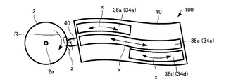
図7は、圧電駆動装置100の動作を説明するための図である。突起部40は、図7に示すように、ローター2の外周に接触している。駆動回路50は、一対の第2電極層36a,36dと第1電極32との間に交流電圧または脈流電圧を印加する。これにより、圧電体層34a,34dは、図7の矢印xの方向に伸縮する。これに応じて、シリコン基板10は、シリコン基板10の平面内で屈曲振動(例えば、圧電素子30に電圧が印加されていない状態でのシリコン基板10の短手方向Bに沿って屈曲振動)して蛇行形状(S字形状)に変形する。さらに、駆動回路50は、第2電極層36eと第1電極32との間に交流電圧または脈流電圧を印加する。これにより、圧電体層34eは、図7の矢印yの方向に伸縮する。これにより、シリコン基板10は、シリコン基板10の平面内で縦振動(例えば、圧電素子30に電圧が印加されていない状態でのシリコン基板10の長手方向Aに沿って縦振動)する。上記のようなシリコン基板10の屈曲振動および縦振動によって、突起部40は、図7の矢印zのように楕円運動する。その結果、ローター2は、その中心2aの周りに所定の方向R(図7では時計回り方向)に回転する。
FIG. 7 is a diagram for explaining the operation of the
なお、駆動回路50が、一対の第2電極層36b,36cと第1電極32との間に交流電圧または脈流電圧を印加する場合には、ローター2は、方向Rとは反対方向(計回り方向)に回転する。
When the
また、シリコン基板10の屈曲振動の共振周波数と縦振動の共振周波数とは、同じであることが好ましい。これにより、効率よくローター2を回転させることができる。
Moreover, it is preferable that the resonance frequency of the flexural vibration and the resonance frequency of the longitudinal vibration of the
圧電駆動装置100は、例えば、以下の特徴を有する。
The
圧電駆動装置100では、シリコン基板10の短手方向のヤング率は、シリコン基板10の長手方向のヤング率よりも小さい。このように、圧電駆動装置100では、シリコン基板10においてヤング率が小さい方向を、長手方向ではなく短手方向にすることによって、シリコン基板10の短手方向に沿った屈曲振動の振幅を大きくすることができ、高出力化を図ることができる。
In the
ここで、シリコン基板の短手方向に沿った屈曲振動の振幅は、大きければ大きいほど、圧電駆動装置の出力を高くすることができる。一方、シリコン基板の長手方向に沿った縦振動は、ローターと突起部との接触および離間に作用し、屈曲振動に比べて圧電駆動装置の出力に影響しない。そこで、圧電駆動装置100では、短手方向のヤング率が長手方向
のヤング率よりも小さくなるようにシリコン基板10を形成することにより、シリコン基板10の短手方向に沿った屈曲振動の振幅を大きくすることができ、高出力化を図ることができる。
Here, the larger the amplitude of the bending vibration along the short direction of the silicon substrate, the higher the output of the piezoelectric driving device. On the other hand, the longitudinal vibration along the longitudinal direction of the silicon substrate acts on the contact and separation between the rotor and the protrusion, and does not affect the output of the piezoelectric driving device compared to the bending vibration. Therefore, in the
圧電駆動装置100では、シリコン基板10は、{110}基板である。そのため、シリコン基板10は、シリコン基板の面内において直交する2方向のヤング率を、異ならせることができる(後述する実験例参照)。圧電駆動装置100では、シリコン基板の面内において直交する2方向に、シリコン基板10の長手方向および短手方向をそろえることができる。
In the
圧電駆動装置100では、圧電体34の厚さは、50nm以上20μm以下である。そのため、圧電駆動装置100では、圧電体34にクラックが発生することを抑制しつつ、高出力化を図ることができる。
In the
なお、上記の例では、突起部40は、シリコン基板10の長手方向の先端部12に設けられていたが、本発明に係る圧電駆動装置は、ステンレス鋼などからなる金属板を有し、突起部40は、該金属板の長手方向の先端部に設けられていてもよい。この場合、シリコン基板10は、金属板上に設けられる。ただし、短手方向のヤング率が長手方向のヤング率よりも小さくなるようにシリコン基板10を形成することにより、圧電駆動装置の高出力化を図るためには、上述した圧電駆動装置100のように、金属板は設けられていないことが好ましい。
In the above example, the
2. 圧電駆動装置の製造方法
次に、本実施形態に係る圧電駆動装置100の製造方法について、図面を参照しながら説明する。図8は、本実施形態に係る圧電駆動装置100の製造方法を説明するためのフローチャートである。図9は、本実施形態に係る圧電駆動装置100の製造工程を模式的に示す平面図である。
2. Next, a method for manufacturing the
図9に示すように、面内において直交する2方向のヤング率が互いに異なるシリコンウェハー4を準備する(S1)。図9に示す例では、シリコンウェハー4は、(110)面で切り出されたシリコンウェハーであり、<110>方向(シリコン基板10の長手方向Aとなる方向)のヤング率と、<100>方向(シリコン基板10の短手方向Bとなる方向)のヤング率とは、異なる。
As shown in FIG. 9, silicon wafers 4 having different Young's moduli in two directions orthogonal in the plane are prepared (S1). In the example shown in FIG. 9, the silicon wafer 4 is a silicon wafer cut out on the (110) plane, and has a Young's modulus in the <110> direction (the direction in which the
図4に示すように、シリコンウェハー4上に、圧電素子30を形成する(S2)。具体的には、シリコンウェハー上に第1電極32を形成し、第1電極32上に圧電体34を形成し、圧電体34上に第2電極36を形成する。第1電極32および第2電極36は、例えば、スパッタ法、CVD(Chemical Vapor Deposition)法、めっき法により導電層を成膜し、該導電層を、フォトリソグラフィーおよびエッチングによってパターニングすることにより形成される。圧電体34は、例えば、ゾルゲル法、MOD(Metal Organic Deposition)法により絶縁層を成膜し、該絶縁層を、フォトリソグラフィーおよびエッチングによってパターニングすることにより形成される。
As shown in FIG. 4, the
次に、シリコンウェハー4を加工して、シリコン基板10と、取付部20と、接続部22と、圧電素子30と、を有するチップ110(図1および図2参照)を取り出す(S3)。具体的には、シリコンウェハー4を、フォトリソグラフィーおよびエッチングすることによって、チップ110を取り出す。
Next, the silicon wafer 4 is processed, and the chip 110 (see FIGS. 1 and 2) having the
図4および図5に示すように、シリコンウェハー4上に多数のチップ110を配列する
ことで、1枚のシリコンウェハー4から多数のチップ110を取り出すことができる。工程S2およびS3において、チップ110をどのような向きに配列するかは、シリコン基板10のヤング率を考慮して決定される。具体的には、シリコン基板10の短手方向のヤング率が、シリコン基板10の長手方向のヤング率よりも小さくなるように、シリコンウェハー4内にチップ110を配列する。
As shown in FIGS. 4 and 5, a large number of
図1および図2に示すように、チップ110の長手方向の先端部(図示の例では、シリコン基板10の長手方向の先端部)12に、突起部40を取り付ける(S4)。具体的には、接着剤を用いて、先端部12に突起部40を接着させる。
As shown in FIGS. 1 and 2, the
以上の工程により、圧電駆動装置100を製造することができる。
The
圧電駆動装置100の製造方法では、シリコン基板10の短手方向のヤング率が、シリコン基板10の長手方向のヤング率よりも小さくなるように、シリコンウェハー4内にチップ110を配列する。そのため、高出力化を図ることができる圧電駆動装置100を製造することができる。
In the method for manufacturing the
3. 実験例
以下に実験例を示し、本発明をより具体的に説明する。なお、本発明は、以下の実験例によって何ら限定されるものではない。
3. Experimental Example An experimental example is shown below to describe the present invention more specifically. The present invention is not limited by the following experimental examples.
実験例として、シリコン(110)ウェハー((110)面で切り出されたシリコンウェハー)の面内方向におけるヤング率を計算した。ヤング率は、弾性スティッフネスの行列を用いて計算した。図10は、ヤング率を計算する際に用いたシリコンの基本定数を示す表である。図10において、「cij」はスティッフネスを示しており、「sij」はコンプライアンスを示している。 As an experimental example, the Young's modulus in the in-plane direction of a silicon (110) wafer (a silicon wafer cut out by the (110) plane) was calculated. Young's modulus was calculated using an elastic stiffness matrix. FIG. 10 is a table showing the basic constants of silicon used when calculating the Young's modulus. In FIG. 10, “cij” indicates the stiffness, and “sij” indicates the compliance.
図11および図12は、上記の方法で計算したシリコン(110)ウェハーにおけるヤング率の面内方向の分布を示す図である。図11および図12において、太線でヤング率の分布を示している。図11および図12では、オリフラを[−111]方向とした。 11 and 12 are diagrams showing the in-plane distribution of Young's modulus in the silicon (110) wafer calculated by the above method. In FIGS. 11 and 12, the Young's modulus distribution is indicated by a bold line. In FIGS. 11 and 12, the orientation flat is in the [−111] direction.
図11に示すように、[001]方向のヤング率は、シリコン(110)ウェハーにおいて最も小さく、130.8GPaであった。また、[001]方向と直交する[−110]方向のヤング率は、169.7GPaであった。したがって、図11に示すように、圧電駆動装置を構成するシリコン基板10の長手方向を[−110]方向とし、短手方向を[001]方向とすることにより、シリコン基板10の短手方向のヤング率を、シリコン基板10の長手方向のヤング率よりも大きくすることができる。特に、[001]方向は、シリコン(110)ウェハーにおいて最もヤング率が小さい方向なので、短手方向に沿った屈曲振動の振幅を、シリコン(110)ウェハーから形成されるシリコン基板10において、最も大きくすることができる。
As shown in FIG. 11, the Young's modulus in the [001] direction was the smallest in the silicon (110) wafer and was 130.8 GPa. The Young's modulus in the [−110] direction orthogonal to the [001] direction was 169.7 GPa. Therefore, as shown in FIG. 11, the longitudinal direction of the
図12に示すように、[1−12]方向のヤング率は、169.7GPaであった。また、[1−12]方向と直交する[−111]方向のヤング率は、188.4GPaであった。したがって、図12に示すように、圧電駆動装置を構成するシリコン基板10の長手方向を[−111]方向とし、短手方向を[1−12]方向とすることにより、シリコン基板10の短手方向のヤング率を、シリコン基板10の長手方向のヤング率よりも大きくすることができる。[−111]方向は、シリコン(110)ウェハーにおいて最もヤング率が大きい方向である。なお、図11および図12に示すように、[1−11]方向のヤング率は、[−111]方向のヤング率と同じで、188.4GPaであった。
As shown in FIG. 12, the Young's modulus in the [1-12] direction was 169.7 GPa. The Young's modulus in the [−111] direction orthogonal to the [1-12] direction was 188.4 GPa. Therefore, as shown in FIG. 12, by setting the longitudinal direction of the
4. 圧電駆動装置を用いた装置
本発明に係る圧電駆動装置は、共振を利用することで被駆動体に対して大きな力を与えることができるものであり、各種の装置に適用可能である。本発明に係る圧電駆動装置は、例えば、ロボット(電子部品搬送装置(ICハンドラー)も含む)、投薬用ポンプ、時計のカレンダー送り装置、印刷装置の紙送り機構等の各種の機器における駆動装置として用いることが出来る。以下、代表的な実施の形態について説明する。以下では、本発明に係る圧電駆動装置として、圧電駆動装置100を含む装置について説明する。
4). Device Using Piezoelectric Drive Device The piezoelectric drive device according to the present invention can apply a large force to a driven body by utilizing resonance, and can be applied to various devices. The piezoelectric drive device according to the present invention is, for example, as a drive device in various devices such as a robot (including an electronic component transfer device (IC handler)), a dosing pump, a calendar feeding device for a clock, and a paper feeding mechanism for a printing device. Can be used. Hereinafter, representative embodiments will be described. Hereinafter, an apparatus including the
4.1. ロボット
図13は、圧電駆動装置100を利用したロボット2050を説明するための図である。ロボット2050は、複数本のリンク部2012(「リンク部材」とも呼ぶ)と、それらリンク部2012の間を回動または屈曲可能な状態で接続する複数の関節部2020と、を備えたアーム2010(「腕部」とも呼ぶ)を有している。
4.1. Robot FIG. 13 is a diagram for explaining a
それぞれの関節部2020には、圧電駆動装置100が内蔵されており、圧電駆動装置100を用いて関節部2020を任意の角度だけ回動または屈曲させることが可能である。アーム2010の先端には、ロボットハンド2000が接続されている。ロボットハンド2000は、一対の把持部2003を備えている。ロボットハンド2000にも圧電駆動装置100が内蔵されており、圧電駆動装置100を用いて把持部2003を開閉して物を把持することが可能である。また、ロボットハンド2000とアーム2010との間にも圧電駆動装置100が設けられており、圧電駆動装置100を用いてロボットハンド2000をアーム2010に対して回転させることも可能である。
Each
図14は、図13に示したロボット2050の手首部分を説明するための図である。手首の関節部2020は、手首回動部2022を挟持しており、手首回動部2022に手首のリンク部2012が、手首回動部2022の中心軸O周りに回動可能に取り付けられている。手首回動部2022は、圧電駆動装置100を備えており、圧電駆動装置100は、手首のリンク部2012およびロボットハンド2000を中心軸O周りに回動させる。ロボットハンド2000には、複数の把持部2003が立設されている。把持部2003の基端部はロボットハンド2000内で移動可能となっており、この把持部2003の根元の部分に圧電駆動装置100が搭載されている。このため、圧電駆動装置100を動作させることで、把持部2003を移動させて対象物を把持することができる。なお、ロボットとしては、単腕のロボットに限らず、腕の数が2以上の多腕ロボットにも圧電駆動装置100を適用可能である。
FIG. 14 is a view for explaining a wrist portion of the
ここで、手首の関節部2020やロボットハンド2000の内部には、圧電駆動装置100の他に、力覚センサーやジャイロセンサー等の各種装置に電力を供給する電力線や、信号を伝達する信号線等が含まれ、非常に多くの配線が必要になる。したがって、関節部2020やロボットハンド2000の内部に配線を配置することは非常に困難だった。しかしながら、圧電駆動装置100は、通常の電動モーターよりも駆動電流を小さくできるので、関節部2020(特に、アーム2010の先端の関節部)やロボットハンド2000のような小さな空間でも配線を配置することが可能になる。
Here, in the wrist joint 2020 and the
4.2. ポンプ
図15は、圧電駆動装置100を利用した送液ポンプ2200の一例を示す説明するための図である。送液ポンプ2200は、ケース2230内に、リザーバー2211と、チューブ2212と、圧電駆動装置100と、ローター2222と、減速伝達機構2223と、カム2202と、複数のフィンガー2213,2214,2215,2216,2217,2218,2219と、が設けられている。
4.2. Pump FIG. 15 is a diagram for explaining an example of a
リザーバー2211は、輸送対象である液体を収容するための収容部である。チューブ2212は、リザーバー2211から送り出される液体を輸送するための管である。圧電駆動装置100の突起部40は、ローター2222の側面に押し付けた状態で設けられており、圧電駆動装置500がローター2222を回転駆動する。ローター2222の回転力は減速伝達機構2223を介してカム2202に伝達される。フィンガー2213から2219はチューブ2212を閉塞させるための部材である。カム2202が回転すると、カム2202の突起部2202Aによってフィンガー2213から2219が順番に放射方向外側に押される。フィンガー2213から2219は、輸送方向上流側(リザーバー2211側)から順にチューブ2212を閉塞する。これにより、チューブ2212内の液体が順に下流側に輸送される。こうすれば、ごく僅かな量を精度良く送液可能で、しかも小型な送液ポンプ2200を実現することができる。
The
なお、各部材の配置は図示されたものには限られない。また、フィンガーなどの部材を備えず、ローター2222に設けられたボールなどがチューブ2212を閉塞する構成であってもよい。上記のような送液ポンプ2200は、インシュリンなどの薬液を人体に投与する投薬装置などに活用できる。ここで、圧電駆動装置100を用いることにより、通常の電動モーターよりも駆動電流を小さくできるので、投薬装置の消費電力を抑制することができる。したがって、投薬装置を電池駆動する場合は、特に有効である。
In addition, arrangement | positioning of each member is not restricted to what was illustrated. Further, a member such as a finger may not be provided, and a ball or the like provided on the
本発明は、実施の形態で説明した構成と実質的に同一の構成(例えば、機能、方法及び結果が同一の構成、あるいは目的及び効果が同一の構成)を含む。また、本発明は、実施の形態で説明した構成の本質的でない部分を置き換えた構成を含む。また、本発明は、実施の形態で説明した構成と同一の作用効果を奏する構成又は同一の目的を達成することができる構成を含む。また、本発明は、実施の形態で説明した構成に公知技術を付加した構成を含む。 The present invention includes configurations that are substantially the same as the configurations described in the embodiments (for example, configurations that have the same functions, methods, and results, or configurations that have the same objects and effects). In addition, the invention includes a configuration in which a non-essential part of the configuration described in the embodiment is replaced. In addition, the present invention includes a configuration that exhibits the same operational effects as the configuration described in the embodiment or a configuration that can achieve the same object. Further, the invention includes a configuration in which a known technique is added to the configuration described in the embodiment.
2…ローター、2a…中心、4…シリコンウェハー、10…シリコン基板、12…先端部、20…取付部、22…接続部、24…ネジ、30…圧電素子、32…第1電極、34…圧電体、34a,34b,34c,34d,34e…圧電体層、36…第2電極、36a,36b,36c,36d,36e…第2電極層、40…突起部、50…駆動回路、60,62,70,72,74,76…配線、100…圧電駆動装置、101…モーター、110…チップ、2000…ロボットハンド、2003…把持部、2010…アーム、2012…リンク部、2020…関節部、2050…ロボット、2200…送液ポンプ、2202…カム、2202A…突起部、2211…リザーバー、2212…チューブ、2213,2214,2215,2216,2217,2218,2219…フィンガー、2222…ローター、2223…減速伝達機構、2230…ケース
DESCRIPTION OF
Claims (13)
前記シリコン基板上に設けられ、第1電極と、第2電極と、前記第1電極と前記第2電極との間に位置する圧電体と、を有する圧電素子と、
前記長手方向の先端部に設けられ、被駆動体に接触する突起部と、
を含み、
前記シリコン基板の前記短手方向のヤング率は、前記シリコン基板の前記長手方向のヤング率よりも小さい、圧電駆動装置。 A silicon substrate having a longitudinal direction and a transverse direction orthogonal to the longitudinal direction;
A piezoelectric element provided on the silicon substrate and having a first electrode, a second electrode, and a piezoelectric body positioned between the first electrode and the second electrode;
A protrusion provided at the distal end in the longitudinal direction and in contact with the driven body;
Including
The piezoelectric drive device, wherein the Young's modulus in the short direction of the silicon substrate is smaller than the Young's modulus in the longitudinal direction of the silicon substrate.
前記シリコン基板は、{110}基板である、圧電駆動装置。 In claim 1,
The piezoelectric drive device, wherein the silicon substrate is a {110} substrate.
前記シリコン基板の前記長手方向は、<110>方向であり、
前記シリコン基板の前記短手方向は、<100>方向である、圧電駆動装置。 In claim 2,
The longitudinal direction of the silicon substrate is a <110> direction,
The piezoelectric drive device, wherein the lateral direction of the silicon substrate is a <100> direction.
前記シリコン基板の前記長手方向は、<111>方向であり、
前記シリコン基板の前記短手方向は、<112>方向である、圧電駆動装置。 In claim 2,
The longitudinal direction of the silicon substrate is a <111> direction,
The piezoelectric drive device, wherein the lateral direction of the silicon substrate is a <112> direction.
前記圧電体の厚さは、50nm以上20μm以下である、圧電駆動装置。 In any one of Claims 1 thru | or 4,
The piezoelectric driving device, wherein the piezoelectric body has a thickness of 50 nm or more and 20 μm or less.
前記シリコンウェハー上に、第1電極と、第2電極と、前記第1電極と前記第2電極との間に位置する圧電体と、を有する圧電素子を形成する工程と、
前記シリコンウェハーを加工して、長手方向と前記長手方向と直交する短手方向とを有するシリコン基板と、前記シリコン基板上に形成された前記圧電素子と、を有するチップを取り出す工程と、
前記チップの前記長手方向の先端部に、被駆動体に接触する突起部を取り付ける工程と、
を含み、
前記シリコン基板の前記短手方向のヤング率が、前記シリコン基板の前記長手方向のヤング率よりも小さくなるように、前記シリコンウェハー内に前記チップを配列する、圧電駆動装置の製造方法。 Preparing silicon wafers having different Young's moduli in two directions perpendicular to each other in a plane;
Forming a piezoelectric element having a first electrode, a second electrode, and a piezoelectric body located between the first electrode and the second electrode on the silicon wafer;
Processing the silicon wafer to take out a chip having a silicon substrate having a longitudinal direction and a transverse direction orthogonal to the longitudinal direction, and the piezoelectric element formed on the silicon substrate;
Attaching a protrusion contacting the driven body to the tip in the longitudinal direction of the chip;
Including
A method of manufacturing a piezoelectric drive device, wherein the chips are arranged in the silicon wafer such that a Young's modulus in the short direction of the silicon substrate is smaller than a Young's modulus in the longitudinal direction of the silicon substrate.
前記シリコン基板は、{110}基板である、圧電駆動装置の製造方法。 In claim 6,
The method for manufacturing a piezoelectric driving device, wherein the silicon substrate is a {110} substrate.
前記シリコン基板の前記長手方向は、<110>方向であり、
前記シリコン基板の前記短手方向は、<100>方向である、圧電駆動装置の製造方法。 In claim 7,
The longitudinal direction of the silicon substrate is a <110> direction,
The method for manufacturing a piezoelectric driving device, wherein the short direction of the silicon substrate is a <100> direction.
前記シリコン基板の前記長手方向は、<111>方向であり、
前記シリコン基板の前記短手方向は、<112>方向である、圧電駆動装置の製造方法。 In claim 7,
The longitudinal direction of the silicon substrate is a <111> direction,
The method for manufacturing a piezoelectric driving device, wherein the lateral direction of the silicon substrate is a <112> direction.
前記圧電体の厚さは、50nm以上20μm以下である、圧電駆動装置の製造方法。 In any one of Claims 6 thru | or 9,
The method for manufacturing a piezoelectric driving device, wherein the piezoelectric body has a thickness of 50 nm to 20 μm.
前記圧電駆動装置によって回転されるローターと、
を含む、モーター。 A piezoelectric driving device according to any one of claims 1 to 5,
A rotor rotated by the piezoelectric drive device;
Including a motor.
複数の前記リンク部を接続する関節部と、
複数の前記リンク部を前記関節部で回動させる請求項1ないし5のいずれか1項に記載の圧電駆動装置と、
を含む、ロボット。 A plurality of link parts;
A joint part connecting a plurality of the link parts;
The piezoelectric driving device according to any one of claims 1 to 5, wherein a plurality of the link portions are rotated by the joint portions,
Including robots.
液体を輸送するチューブと、
前記圧電駆動装置の駆動によって前記チューブを閉鎖する複数のフィンガーと、
を含む、ポンプ。 A piezoelectric driving device according to any one of claims 1 to 5,
A tube that transports the liquid;
A plurality of fingers for closing the tube by driving the piezoelectric driving device;
Including a pump.
Priority Applications (1)
| Application Number | Priority Date | Filing Date | Title |
|---|---|---|---|
| JP2015189395A JP2017069998A (en) | 2015-09-28 | 2015-09-28 | Piezoelectric drive device, manufacturing method for the same, motor, robot and pump |
Applications Claiming Priority (1)
| Application Number | Priority Date | Filing Date | Title |
|---|---|---|---|
| JP2015189395A JP2017069998A (en) | 2015-09-28 | 2015-09-28 | Piezoelectric drive device, manufacturing method for the same, motor, robot and pump |
Publications (2)
| Publication Number | Publication Date |
|---|---|
| JP2017069998A true JP2017069998A (en) | 2017-04-06 |
| JP2017069998A5 JP2017069998A5 (en) | 2018-09-20 |
Family
ID=58493008
Family Applications (1)
| Application Number | Title | Priority Date | Filing Date |
|---|---|---|---|
| JP2015189395A Withdrawn JP2017069998A (en) | 2015-09-28 | 2015-09-28 | Piezoelectric drive device, manufacturing method for the same, motor, robot and pump |
Country Status (1)
| Country | Link |
|---|---|
| JP (1) | JP2017069998A (en) |
Cited By (4)
| Publication number | Priority date | Publication date | Assignee | Title |
|---|---|---|---|---|
| JP2018199293A (en) * | 2017-05-29 | 2018-12-20 | セイコーエプソン株式会社 | Piezoelectric device, liquid discharge head, liquid discharge device |
| JP2018199292A (en) * | 2017-05-29 | 2018-12-20 | セイコーエプソン株式会社 | Piezoelectric device, liquid discharge head, liquid discharge device |
| JP2019092358A (en) * | 2017-11-17 | 2019-06-13 | セイコーエプソン株式会社 | Piezoelectric driving device, piezoelectric motor, robot, electronic component conveying device, printer, and projector |
| CN112448609A (en) * | 2019-08-27 | 2021-03-05 | 精工爱普生株式会社 | Piezoelectric driving device and robot |
-
2015
- 2015-09-28 JP JP2015189395A patent/JP2017069998A/en not_active Withdrawn
Cited By (6)
| Publication number | Priority date | Publication date | Assignee | Title |
|---|---|---|---|---|
| JP2018199293A (en) * | 2017-05-29 | 2018-12-20 | セイコーエプソン株式会社 | Piezoelectric device, liquid discharge head, liquid discharge device |
| JP2018199292A (en) * | 2017-05-29 | 2018-12-20 | セイコーエプソン株式会社 | Piezoelectric device, liquid discharge head, liquid discharge device |
| JP2019092358A (en) * | 2017-11-17 | 2019-06-13 | セイコーエプソン株式会社 | Piezoelectric driving device, piezoelectric motor, robot, electronic component conveying device, printer, and projector |
| JP7031244B2 (en) | 2017-11-17 | 2022-03-08 | セイコーエプソン株式会社 | Piezoelectric drives, piezoelectric motors, robots, electronic component conveyors, printers and projectors |
| CN112448609A (en) * | 2019-08-27 | 2021-03-05 | 精工爱普生株式会社 | Piezoelectric driving device and robot |
| CN112448609B (en) * | 2019-08-27 | 2023-06-16 | 精工爱普生株式会社 | Piezoelectric driving device and robot |
Similar Documents
| Publication | Publication Date | Title |
|---|---|---|
| US10644222B2 (en) | Piezoelectric drive apparatus for motor and method for manufacturing the same, motor, robot, and pump | |
| JP2017017916A (en) | Piezoelectric driving device, robot, and driving method of piezoelectric driving device | |
| US20160241165A1 (en) | Piezoelectric drive device, robot, and drive method thereof | |
| JP2017092326A (en) | Electric device, piezoelectric motor, robot, hand and feed pump | |
| JP2017069998A (en) | Piezoelectric drive device, manufacturing method for the same, motor, robot and pump | |
| US10236795B2 (en) | Piezoelectric driving device for motor, motor, robot, and pump | |
| US10601345B2 (en) | Piezoelectric driving device, motor, robot, and pump | |
| US9712087B2 (en) | Piezoelectric element drive circuit and robot | |
| JP6459291B2 (en) | Piezoelectric driving device and driving method thereof, robot and driving method thereof | |
| JP6601174B2 (en) | Piezoelectric actuators, stacked actuators, piezoelectric motors, robots, hands and liquid pumps | |
| JP2016040984A (en) | Piezoelectric drive device and drive method of the same, robot and drive method of the robot | |
| JP2016040990A (en) | Piezoelectric drive device, robot, and drive method therefor | |
| JP6432204B2 (en) | Piezoelectric drive device, robot, and drive method thereof | |
| JP6662007B2 (en) | Piezo drives, motors, robots, and pumps | |
| JP6641910B2 (en) | Piezoelectric driving device and manufacturing method thereof, motor, robot, and pump | |
| JP6641943B2 (en) | Piezoelectric drive device for motor and method of manufacturing the same, motor, robot, and pump | |
| JP6693120B2 (en) | Piezoelectric drive device and manufacturing method thereof, motor, robot, and pump | |
| JP2017103956A (en) | Piezoelectric driving device, motor, robot, and pump | |
| JP2017005925A (en) | Piezoelectric driving device for motor, motor, robot and pump | |
| JP2017103954A (en) | Piezoelectric driving device, motor, robot, and pump | |
| WO2016147539A1 (en) | Method for manufacturing piezoelectric element, piezoelectric element, piezoelectric drive device, robot, and pump | |
| JP6432369B2 (en) | Piezoelectric driving device, robot, and robot driving method | |
| JP6641911B2 (en) | Piezoelectric driving device and manufacturing method thereof, motor, robot, and pump | |
| JP6413461B2 (en) | Piezoelectric driving device and driving method thereof, robot and driving method thereof | |
| JP2016174024A (en) | Piezoelectric element for ultrasonic motor and method of manufacturing the same, ultrasonic motor, robot, and pump |
Legal Events
| Date | Code | Title | Description |
|---|---|---|---|
| A521 | Request for written amendment filed |
Free format text: JAPANESE INTERMEDIATE CODE: A523 Effective date: 20180806 |
|
| A621 | Written request for application examination |
Free format text: JAPANESE INTERMEDIATE CODE: A621 Effective date: 20180806 |
|
| A131 | Notification of reasons for refusal |
Free format text: JAPANESE INTERMEDIATE CODE: A131 Effective date: 20190424 |
|
| A977 | Report on retrieval |
Free format text: JAPANESE INTERMEDIATE CODE: A971007 Effective date: 20190426 |
|
| A761 | Written withdrawal of application |
Free format text: JAPANESE INTERMEDIATE CODE: A761 Effective date: 20190621 |