JP2017016285A - Data control apparatus which shares buffer among plural data processing units, and control method - Google Patents
Data control apparatus which shares buffer among plural data processing units, and control method Download PDFInfo
- Publication number
- JP2017016285A JP2017016285A JP2015130617A JP2015130617A JP2017016285A JP 2017016285 A JP2017016285 A JP 2017016285A JP 2015130617 A JP2015130617 A JP 2015130617A JP 2015130617 A JP2015130617 A JP 2015130617A JP 2017016285 A JP2017016285 A JP 2017016285A
- Authority
- JP
- Japan
- Prior art keywords
- data
- intermediate buffer
- buffer
- status information
- unit
- Prior art date
- Legal status (The legal status is an assumption and is not a legal conclusion. Google has not performed a legal analysis and makes no representation as to the accuracy of the status listed.)
- Granted
Links
- 239000000872 buffer Substances 0.000 title claims abstract description 392
- 238000000034 method Methods 0.000 title claims description 94
- 238000001514 detection method Methods 0.000 claims 2
- 238000004891 communication Methods 0.000 abstract description 19
- 230000001360 synchronised effect Effects 0.000 abstract description 10
- 230000008569 process Effects 0.000 description 80
- 230000005540 biological transmission Effects 0.000 description 31
- 238000010586 diagram Methods 0.000 description 13
- 230000015654 memory Effects 0.000 description 10
- 230000007704 transition Effects 0.000 description 5
- 238000006243 chemical reaction Methods 0.000 description 3
- 230000006870 function Effects 0.000 description 3
- 238000004590 computer program Methods 0.000 description 2
- 230000000694 effects Effects 0.000 description 2
- 230000007423 decrease Effects 0.000 description 1
- 230000007246 mechanism Effects 0.000 description 1
- 230000004044 response Effects 0.000 description 1
- 230000002195 synergetic effect Effects 0.000 description 1
Images


Abstract
Description
本発明は、データ処理装置及びその制御方法に関し、特に、データ処理部へ供給するデータを保持するバッファを、複数のデータ処理部で共有する場合のデータ制御装置、制御方法に関する。 The present invention relates to a data processing device and a control method thereof, and more particularly to a data control device and a control method in the case where a buffer that holds data to be supplied to a data processing unit is shared by a plurality of data processing units.
システムバスにCPU(Central Processing Unit)、DRAM(Random Access Memory)、データ処理部など様々なモジューが接続されている場合、システムバス上のデータ通信が多くなると、システムバスの帯域が圧迫され、スムーズなデータ通信を阻害してしまう。そこで、例えばシングルコアプロセッサではキャッシュメモリにDRAM上のデータを移し、キャッシュメモリとコアの間でデータ通信することでDRAMとコアの間で行われるデータ通信を低減している。しかし、複数のシングルコアプロセッサがキャッシュ上のデータを共有するにはDRAMを介して通信する必要がある。 When various modules such as CPU (Central Processing Unit), DRAM (Random Access Memory), and data processing unit are connected to the system bus, if the data communication on the system bus increases, the bandwidth of the system bus is compressed and smooth. Data communication will be hindered. Thus, for example, in a single core processor, data communication between the DRAM and the core is reduced by transferring data on the DRAM to the cache memory and performing data communication between the cache memory and the core. However, in order for a plurality of single core processors to share data on the cache, it is necessary to communicate via DRAM.
このため、複数のコア間でデータを共有する場合には、DRAMとの通信が肥大化してシステムバスの帯域を圧迫してしまう。そこで、マルチコアプロセッサのように複数のコアでキャッシュメモリのデータを共有するコヒーレンシ制御を行い、システムバス上でのデータ通信を低減するといった方法が開発されている(特許文献1)。また、特許文献2に示されるCELLプロセッサでもシステムバスとのデータ通信を低減する施策がなされている。
For this reason, when data is shared among a plurality of cores, communication with the DRAM is enlarged, and the bandwidth of the system bus is compressed. Therefore, a method has been developed in which coherency control is performed in which cache memory data is shared by a plurality of cores, such as a multi-core processor, to reduce data communication on the system bus (Patent Document 1). The CELL processor disclosed in
CELLプロセッサは演算部とLS(Local Store)を持つSPE(Synergistic Processor Element)を複数搭載し、これらはSPE間で高速なデータ通信を行うEIB(Element Interconnect Bus)で接続されている。また、SPEがDRAMとデータ通信する場合はEIBに接続されるMIC(Memory Interface Controller)からシステムバスを介して行われる。このような構成であることから、あるSPEのLSに保持されているデータを他のSPEのLSに受け渡す場合は、EIBを介して行われる。つまり、SPE間ではシステムバスとは独立した高速データ通信バスのEIBが用いられるため、システムバス上のデータ通信を低減する事が出来る。 The CELL processor includes a plurality of SPEs (Synergistic Processor Elements) having an arithmetic unit and an LS (Local Store), and these are connected by an EIB (Element Interconnect Bus) that performs high-speed data communication between the SPEs. Further, when the SPE performs data communication with the DRAM, it is performed from a MIC (Memory Interface Controller) connected to the EIB via the system bus. Because of such a configuration, when data held in the LS of a certain SPE is transferred to the LS of another SPE, it is performed via the EIB. That is, since the EIB, which is a high-speed data communication bus independent of the system bus, is used between the SPEs, data communication on the system bus can be reduced.
しかしながら、マルチコアプロセッサではコヒーレンシ制御を行う際、コヒーレンシ制御に数クロックサイクルの制御が必要となり、データ共有のオーバーヘッドとなり得た。また、CELLプロセッサではあるSPEのLSで保持しているデータを他のSPEが参照するには、EIBを介したデータ通信が必要となるため、データ通信制御に多くのクロックサイクルを消費していた。
本発明は、上記のような課題を鑑みて、ローカルメモリを持つ系を複数搭載するシステムでも簡易な構成で高速なデータ共有を行うバッファの制御方法及び制御装置を提供する。
However, in multi-core processors, when performing coherency control, control of several clock cycles is required for coherency control, which may be an overhead of data sharing. In addition, since the CELL processor requires data communication via the EIB in order for other SPEs to refer to data held in the LS of a certain SPE, many clock cycles are consumed for data communication control. .
In view of the above-described problems, the present invention provides a buffer control method and control apparatus that perform high-speed data sharing with a simple configuration even in a system that includes a plurality of systems having local memories.
複数の中間バッファ制御手段を備えるデータ制御装置であって、
前記中間バッファ制御手段は、
DRAMから中間バッファへのデータ転送および前記中間バッファからデータ処理手段へのデータ転送を制御する入力手段と、
前記データ処理手段から前記中間バッファへのデータ転送および前記中間バッファから前記DRAMへのデータ転送を制御する出力手段と、
前記入力手段および前記出力手段のバッファ状態情報を各々保持し、前記バッファ状態情報に応じて、前記入力手段および前記出力手段の動作を制御する同期実行手段とを備え、
前記同期実行手段は、
前記入力手段から実行完了通知を受け取ると、前記入力手段のバッファ状態情報を書込状態と設定し、
前記出力手段から実行完了通知を受け取ると、前記出力手段のバッファ状態情報を読出状態と設定し、
他の中間バッファ制御手段と中間バッファを共有する場合には、該他の中間バッファ制御手段の同期実行手段とバッファ状態情報を相互に送信し、
他の中間バッファ制御手段と中間バッファを共有しない場合には、前記入力手段のバッファ状態情報と前記出力手段のバッファ状態情報を相互に送信し、
同期信号によってそれぞれの同期実行手段のバッファ状態情報を更新する。
A data control device comprising a plurality of intermediate buffer control means,
The intermediate buffer control means includes
Input means for controlling data transfer from the DRAM to the intermediate buffer and data transfer from the intermediate buffer to the data processing means;
Output means for controlling data transfer from the data processing means to the intermediate buffer and data transfer from the intermediate buffer to the DRAM;
Synchronization holding means for holding buffer status information of the input means and the output means, respectively, and controlling operations of the input means and the output means according to the buffer status information,
The synchronization execution means includes
When the execution completion notification is received from the input means, the buffer status information of the input means is set to the write state,
When the execution completion notification is received from the output means, the buffer status information of the output means is set as a read state,
When the intermediate buffer is shared with other intermediate buffer control means, the synchronization execution means of the other intermediate buffer control means and the buffer status information are mutually transmitted,
When the intermediate buffer is not shared with other intermediate buffer control means, the buffer status information of the input means and the buffer status information of the output means are sent to each other,
The buffer status information of each synchronization execution means is updated by the synchronization signal.
複数の中間バッファ制御部にて、中間バッファの状態情報を保持し、中間バッファ状態情報の書込状態信号と読出状態信号、同期信号を各中間バッファ制御部で相互に通信し、同期信号を相互に受信したタイミングで中間バッファ状態情報を更新する。これにより、簡易な構成で複数の中間バッファ制御部で1つの中間バッファを共有でき、高速なデータ共有が可能となる。 A plurality of intermediate buffer control units hold the intermediate buffer state information, and the intermediate buffer control unit communicates the write state signal, the read state signal, and the synchronization signal of the intermediate buffer state information to each other. The intermediate buffer status information is updated at the timing received at the time. As a result, one intermediate buffer can be shared by a plurality of intermediate buffer control units with a simple configuration, and high-speed data sharing becomes possible.
以下、図面を参照して本発明の実施形態を説明する。ただし、本発明は以下の実施形態に限定されるものではない。
<実施例1>
(画像処理装置)
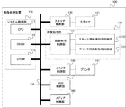
図1は、本発明の第1の実施形態における画像処理装置の一構成例を示すブロック図である。画像処理装置100は、システム制御部110、スキャナ制御部120、画像処理部130、プリンタ制御部140からなる。
システム制御部110は、画像処理装置のシステムバス170に接続された各モジュールを制御するCPU111、画像データや各モジュールの設定値など、一時的なデータを保持するDRAM112、後述する制御用のプログラムを保持するROM113からなる。
Hereinafter, embodiments of the present invention will be described with reference to the drawings. However, the present invention is not limited to the following embodiments.
<Example 1>
(Image processing device)
FIG. 1 is a block diagram illustrating a configuration example of an image processing apparatus according to the first embodiment of the present invention. The
The
スキャナ制御部120は接続されているスキャナ121を制御し、得られた画像データをDMA(Direct Memory Access)転送にてDRAM112に書き出すモジュールである。CPU111からスキャン開始命令を受けると、スキャナ121を起動し、読み取り媒体をスキャンする。スキャナ121はスキャンによってCCDセンサなどから得られたアナログ画像信号に対してアナログ/デジタル変換を行い、デジタル画像データ(以下、画像データと記載する。)を生成する。この画像データをスキャナ制御部120が受信し、DMA転送によってDRAM112に書き出す。以上のスキャン処理を終えたら、スキャン終了信号をCPU111や画像処理部130に送信する。
The
プリンタ制御部140は接続されているプリンタ141を制御し、DRAM上の画像データを印刷媒体に記録させるモジュールである。CPU111からプリント開始命令を受けると、DMA転送でDRAM112からプリント用の画像データを取り出し、プリンタ141を起動する。そして、プリンタ141が備えるプリントヘッダなどからインクを吐出し、印刷媒体に画像を記録する。以上のプリント処理を終えたらプリント終了信号をCPU111に送信する。
The
ここで、扱う画像データはUSBメモリやフラッシュカードなどから読み書きされてもよく、図1のようにシステムバス170にUSB制御部150やメディア制御部160を接続しておき、こちらから画像データをDRAM112に転送しても良い。いずれにしても、これらのモジュールは色々な形で実現できることは明らかで、図示している構成に限定されるものではない。
Here, the image data to be handled may be read and written from a USB memory, a flash card, or the like, and the
画像処理部130は本発明の特徴である中間バッファの制御を含む画像処理制御部131とスキャナ用画像処理回路群132、プリンタ用画像処理回路群133で構成されるデータ制御装置である。画像処理部130は、CPU111から画像処理実行開始の命令を受けると、画像処理制御部131がDMA転送によってDRAM上の画像データの一部を取得し、後に説明する中間バッファに書きこむ。そして、中間バッファで保持しているデータをスキャナ用画像処理回路群132やプリンタ用画像処理回路群133に転送して画像処理を実行する。その後、中間バッファに画像処理結果を書き出し、DMA転送にて中間バッファに保持されている画像処理結果をDRAM112に書き戻す。以上の操作を、画像データ全体に適用する事で画像処理を完了する。
The
ここで、一例としてスキャン処理とプリント処理を連続して実行する際の画像処理装置の動作を簡単に説明する。説明を簡単にするため、DRAM、中間バッファは画像データを保持できるだけ容量があるものとする。まず、CPU111はROM113からプログラムを読み出し、実行を開始する。CPU111はプログラムに従って、スキャナ制御部120、画像処理部130、プリンタ制御部140の設定を行う。
Here, as an example, the operation of the image processing apparatus when the scan process and the print process are continuously executed will be briefly described. In order to simplify the explanation, it is assumed that the DRAM and the intermediate buffer have enough capacity to hold image data. First, the CPU 111 reads a program from the
その後、スキャナ制御部120を起動し、スキャンした画像データをDRAM112に書き込む。その後、画像処理部130を起動し、DRAM112に保持されている画像データに対して適切な画像処理を行わせて、処理結果をDRAM112に書き出す。最後に、プリンタ制御部140を起動し、画像処理されたDRAM上の画像データを読み出し、印刷する。
Thereafter, the
以上のようにしてスキャン処理、プリント処理を実行する。また、システム制御部110はプログラムに従って各モジュールを制御するもので、適切なプログラムを用いることで種々の処理を実現する事が出来るものである。
続けて、DRAM112や中間バッファの容量が画像データ200の全体を保持できない容量における動作について説明する。DRAM112や中間バッファの容量が少ない場合は、画像データを分割して画像処理を行う。
The scan process and the print process are executed as described above. The
Next, an operation in a capacity where the capacity of the
(バンド処理)
家庭用プリンタのように安価に提供しなければならない機器では、ハードウェアのコストを抑えるため、1枚のデジタル画像データ全体を記憶できるだけの容量のメモリを実装できない場合がある。そのため、1枚のデジタル画像データを複数の短冊状のバンド領域に分割し、逐次的にバンド領域のみをメモリ(以下、バンドメモリと称する)に展開して各種の画像処理を施す、いわゆるバンド処理が行われることがある。
(Band processing)
In a device that needs to be provided at a low cost such as a home printer, there is a case where it is not possible to mount a memory having a capacity enough to store one piece of digital image data in order to reduce hardware costs. Therefore, one digital image data is divided into a plurality of strip-shaped band areas, and only the band areas are sequentially developed in a memory (hereinafter referred to as a band memory) to perform various image processing, so-called band processing. May be performed.
ここでは、DRAMは図2に示すバンド領域210の全体を保持することができるだけの容量を持つが、中間バッファの容量はバンド領域の一部しか保持できない容量である場合の動作について説明する。
まず、前述と同様にCPU111はROM113からプログラムを読み出し、スキャナ制御部120、画像処理部130、プリンタ制御部140の設定を行う。その後、スキャナ制御部120を起動し、画像データの一部分であるバンド領域210をスキャンしてDRAM112に書き込む。
Here, although the DRAM has a capacity that can hold the
First, as described above, the CPU 111 reads a program from the
その後、画像処理部130を起動し、バンド領域210に対して画像処理を行う。ただし、画像処理部130の中間バッファはバンド領域の一部を保持できるだけの容量しか持たないため、バンド領域210をバンド分割領域A230、バンド分割領域B231及びバンド分割領域C232の3つに分割して画像処理を適用する。(図2(h)〜(j))
Thereafter, the
まず、画像処理部130はバンド分割領域A230をDRAM112から読み出し、画像処理を適用した画像データをDRAM112に書き出す。
続けて、画像処理部130は次のバンド分割領域B231をDRAM112から読み出し、画像処理を適用した画像データをDRAM112に書き出す。
これを繰り返すことでバンド領域210に対する画像処理を完了する。
その後、プリンタ制御部140を起動し、DRAM上の画像処理されたバンド領域を読み出し、印刷する。
First, the
Subsequently, the
By repeating this, the image processing for the
Thereafter, the
このようにしてバンド領域210(図2(a))の処理が終わったら、続けてバンド領域211(図2(b))をスキャナで読み込み、バンド領域210の処理と同様にバンド領域211を分割して画像処理を行う。
以上の処理を繰り返し、画像全体に適用する事で、DRAM112や中間バッファの容量が画像データ200の全体を保持できない容量の場合でも、画像200全体に対して画像処理を適用する事が出来る。
When the processing of the band area 210 (FIG. 2A) is completed in this way, the band area 211 (FIG. 2B) is read by the scanner, and the band area 211 is divided in the same manner as the processing of the
By repeating the above processing and applying it to the entire image, the image processing can be applied to the
(画像処理部)
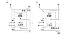
次に図3を用いて画像処理部130の詳細を説明する。
画像処理部130は、上述の通り、画像処理制御部131と、スキャナ用画像処理回路群132と、プリンタ用画像処理回路群133とからなるデータ制御装置である。スキャナ用画像処理回路群132と、プリンタ用画像処理回路群133とは、データ処理部としての役割を担う。
(Image processing unit)
Next, details of the
As described above, the
スキャナ用画像処理回路群132は、接続するスキャナ121ごとのCCDセンサ特性を補正するためのガンマ変換や、スキャン時のノイズを除去するフィルタ等の画像処理回路132−1〜132−nを含む。スキャナ用画像処理回路群132は、中間バッファ制御部a320と接続され、スキャン処理実行時には中間バッファ制御部a320から、各画像処理回路に画像データが入力され、各画像処理回路で演算した結果を中間バッファ制御部a320に出力する。
The scanner image
プリンタ用画像処理回路群133は、画像データを印刷用インクの色空間に変換する色空間変換や、多階調の画像データを低階調で表現する形に変換するハーフトーン処理などの画像処理回路133−1〜133−nを含む。プリンタ用画像処理回路群133は、中間バッファ制御部b330と接続され、プリント処理実行時にはスキャナ用画像処理回路群と同様に、中間バッファ制御部b330と設定コマンドや画像データの入出力を行う。
The image processing circuit group for
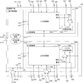
画像処理制御部131は、内蔵する中間バッファを介して、DRAM112と画像処理回路間のデータ通信を制御する回路である。画像処理制御部131は、DMAコントローラ310と、中間バッファ制御部a320と、中間バッファ制御部b330と、中間バッファ群340とで構成される。
The image
DMAコントローラ310は、中間バッファ制御部a、bからのリクエストに応じてDRAM上のデータを中間バッファに書き込む操作と、中間バッファのデータをDRAM112に書き出す操作をDMA転送で行う。DRAM上のどのアドレスにアクセスするか、どの中間バッファにアクセスするかは、中間バッファ制御部a、bからのリクエストで指定される。
The
中間バッファ群340は、画像データを一時的に保持する複数の中間バッファ342−1〜342−4と、各バッファへのアクセスリクエストを調停し、アクセス結果をリクエスト発行元へ送信するアービタ341とから構成される。
アービタ341は、中間バッファ342と、中間バッファ342へのリクエストを発行するDMAコントローラ310と、中間バッファ制御部a320と、中間バッファ制御部b330とに接続される。アービタ341はリクエスト発行元からの中間バッファ342への書き込み、読み出しリクエストを調停し、実行する。具体的には、複数のモジュールから同時に同じバッファへのアクセス要求があった場合には、優先順位の高いモジュールのアクセスから先に実行して行くといった調停を行う。ただし、調停方法についてはこれを限定するものではない。
The
The
中間バッファ制御部a320は、DRAM112と中間バッファとの間の通信、中間バッファ342と画像処理回路との間の通信を制御するモジュールである。中間バッファ制御部a320は、画像入力部321と画像出力部322と、これらの設定、実行管理を行う同期実行部333とから構成される。また、中間バッファ制御部b330も同様の構成、動作であるため、以下、中間バッファ制御部a320を主として説明する。
The intermediate buffer control unit a320 is a module that controls communication between the
(画像入力部)
画像入力部321は、同期実行部323の命令に応じて、中間バッファを操作するリクエストを発行するモジュールである。リクエストには2種類あり、1つはDRAM112から画像データを取得して中間バッファ342へ書き込むリクエストで、DMAコントローラ310に発行するものである。もう一つは、中間バッファ342に保持されている画像データを読み出し、画像処理回路132に送信するリクエストで、中間バッファ群340に発行するものである。
(Image input part)
The
図4(a)を用いて画像入力部321の詳細について説明する。
画像入力部321はDMA受信部411とパケット送信部412で構成される。
Details of the
The
DMA受信部411は、DMAコントローラ310へ発行するリクエストの制御を行う。画像処理時には、同期実行部323からDRAM上の画像データが置かれているアドレスや、どの中間バッファを利用するかが設定される。その後、同期実行部323から実行開始命令を受信すると、設定されたDRAM112のアドレス領域から所定量の画像データを取得し、中間バッファ342へ書き込むようDMAコントローラ310にリクエストを発行する。DMAコントローラ310からリクエストの実行完了を通知されたら、同期実行部323へ実行完了を通知する。
The DMA receiver 411 controls a request issued to the
(パケット送信部)
パケット送信部412は、中間バッファ群340に発行するリクエストと、画像処理回路132へのデータ出力を制御するモジュールである。画像処理時には、同期実行部323からどのバッファを利用するか、扱う画像フォーマットや画像サイズが設定される。その後、同期実行部323からの実行開始命令を受信すると、設定されたいずれかの中間バッファ342から画像フォーマットに合わせてデータを取り出すようリクエストを生成し、中間バッファ群340に発行する。
(Packet transmitter)
The
同時に中間バッファ群340から読み出した画像データに対して、同期実行部323から設定された画像サイズに合わせて画素位置を特定するための情報を付加したパケットデータを生成し、画像処理部132に送信する。送信を完了したら、同期実行部323へ実行完了を通知する。
ここで、パケット送信部412が画像データに付加する画素位置を特定するための情報について図2を用いて説明する。
At the same time, packet data in which information for specifying the pixel position is added to the image data read from the
Here, information for specifying a pixel position added to the image data by the
図2(k)は、パケット送信部412が画像処理部132に送信する画像データ240を示している。パケット送信部412は転送するデータ量として同期実行部323から主走査方向にv画素、副走査方向にh画素の画像データを扱うように設定される。パケット送信部412は画素240−1から副走査方向順に画素データを送信する。h画素目を送信したら主走査方向に1画素移動し、副走査方向に1画素目から順に送信する。
FIG. 2K shows
転送開始時、1画素目の画素240−1のデータを転送する際には、画素位置を特定するための情報として、転送開始信号とラインスタート信号を付加する。
転送終了時、最後の画素240−nのデータを送信する際には、転送終了信号とラインエンド信号を付加する。
また、副走査方向に見たときに1画素目となる画素のデータを送信する際には、ラインスタート信号のみ付加する。
副走査方向に見た時に最終画素となるh画素目の画素のデータを送信する際には、ラインエンド信号のみ付加する。
画素位置を特定するためのこれらの信号は画像処理回路、画像出力部322で利用され、画像出力部322では画像処理後の画像データのサイズを算出する際に用いる。
At the start of transfer, when data of the first pixel 240-1 is transferred, a transfer start signal and a line start signal are added as information for specifying the pixel position.
When the data of the last pixel 240-n is transmitted at the end of transfer, a transfer end signal and a line end signal are added.
In addition, when transmitting data of the first pixel when viewed in the sub-scanning direction, only the line start signal is added.
Only the line end signal is added when transmitting the data of the h-th pixel which is the final pixel when viewed in the sub-scanning direction.
These signals for specifying the pixel position are used by the image processing circuit and the
(画像出力部)
画像出力部322は同期実行部323の命令に応じて、中間バッファを操作するリクエストを発行するモジュールである。リクエストには2種類あり、1つは画像処理回路132で処理した画像データを受信し、中間バッファ342に書き出すリクエストを中間バッファ群340に発行するものである。もう一つは、中間バッファ342に保持されている処理済みの画像データをDRAM112に書き出すリクエストをDMAコントローラ310に発行するものである。ここで、図4(b)を用いて画像出力部322の詳細について説明する。
画像出力部332はパケット受信部422とDMA送信部421で構成されている。
(Image output part)
The
The
(パケット受信部)
パケット受信部422は、画像処理回路132からの画像データを受信し、中間バッファ群340に発行するリクエストを制御するモジュールである。画像処理時には、同期実行部323から、どの中間バッファ342を利用するかといった設定や、扱う画像フォーマットが設定される。
(Packet receiver)
The
その後、同期実行部323から実行開始命令を受信すると、画像処理部132からの画像データを受信し、設定された画像フォーマットに合わせて中間バッファ243にデータを書き込むようリクエストを生成し、中間バッファ群340に発行する。また、画像入力部321で付加された転送終了信号を受信したら、同期実行部323へ実行完了と出力画像サイズを通知する。ここで、出力画像サイズの算出方法と利用方法について図2を用いて説明する。
Thereafter, when an execution start command is received from the
図2(l)に示す画像データ240´は、図2(k)に示す画像データ240を画像処理回路群で処理して得られた画像データであり、パケット受信部で受信される画像データを示している。画像データ240´は主走査方向にv´画素、副走査方向にh´画素の画像データである。パケット受信部422は、画素240−1´から副走査方向順に画素データ受信する。h´画素目の画素を受信したら副走査方向に1画素移動し、主走査方向に1画素目から順に受信する。
The
パケット受信部422では副走査方向に1画素目の画素を受信する際、画像入力部で付加されたラインスタート信号を検知して、受信画素数のカウントを開始する。
続けて画素240−2´、240−3´を受信するごとに受信画素数をカウントアップする。
そして、主走査方向にh´画素目の画素を受信した際には画像入力部321によって付加したラインエンド信号を検知して受信画素数のカウントアップを終了する。
このようにして、パケット受信部422は、画像処理回路で処理されて得られた出力画像のサイズとして主走査方向の画素数h´を算出する。
When the
Each time the pixels 240-2 ′ and 240-3 ′ are received, the number of received pixels is counted up.
When the h'th pixel is received in the main scanning direction, the line end signal added by the
In this way, the
その後、この画素数h´はパケット受信部422を含む画像出力部322から信号5113aにて実行制御部510に送信される。そして、実行制御部510にてDMA受信部411が複数のバンド領域を連続して処理する際のDRAM上のアドレスを算出する際の受信データ量として用いられる。算出したDRAMアドレスは実行制御部510から信号511にてDMA受信部411に設定される。
後で詳細に説明するが、スキャン処理とプリント処理を連続実行する際に、中間バッファ制御部a、bで中間バッファ342を共有する場合における出力画素数の利用方法について説明する。
まず、バンド領域に対して前段のスキャン処理を実行する。
その後、後段のプリント処理を担当する中間バッファ制御部b330で出力画像の画素数h´を算出する。
この画素数h´を前段のスキャン処理を担当する中間バッファ制御部a320の信号線5113bで受信する。
中間バッファ制御部a320は、受信した値(画素数h´)を用いて次に取得するバンド領域のDRAM上のアドレスを算出する。
Thereafter, the pixel number h ′ is transmitted from the
As will be described in detail later, a method of using the number of output pixels when the intermediate buffer control units a and b share the intermediate buffer 342 when the scan process and the print process are continuously executed will be described.
First, the preceding scan process is executed for the band region.
Thereafter, the intermediate buffer control unit b330 in charge of the subsequent printing process calculates the pixel number h ′ of the output image.
The number h ′ of pixels is received by the
The intermediate buffer control unit a320 calculates an address on the DRAM of the band area to be acquired next using the received value (number of pixels h ′).
具体的には、図2(e)に示すように、副走査方向にh画素のバンド領域210に対して画像処理をした結果、副走査方向にh´画素の出力画像データが得られたとする。この場合、実行制御部510は画像出力部422によって算出された画素数h´を用いて、次に処理するバンド領域を算出して、バンド領域220からh´画素分副走査方向に移動したバンド領域221を取得するよう制御する。
この仕組みにより、画像処理回路の中にフィルタのように出力画像のサイズが変化する画像処理があった場合においても、画像処理部130内で自律的にDRAM上のアドレス参照先を切り替えることによって、出力画像の連続性を確保することが出来る。つまり、出力画像の連続性を確保するために、処理するバンド領域を切り替えるごとにCPU111から、実行制御部510の設定を切り替える、という必要が無くなり、CPU111の制御を待つことなく複数のバンド領域を連続して転送する事が可能となる。
この点について以下に詳しく説明する。
Specifically, as shown in FIG. 2E, as a result of performing image processing on the
By this mechanism, even when there is image processing in which the size of the output image changes like a filter in the image processing circuit, by autonomously switching the address reference destination on the DRAM within the
This point will be described in detail below.
図15(a)は、入力画像データ1500と、画像処理部に入力される1つ目の入力バンド領域1511,2つ目の入力バンド領域1521を示す。
図15(b)は、画像処理部から出力される1つ目の出力バンド領域1512,2つ目の出力バンド領域1522を示す。
入力バンド領域1511(のデータ)が処理されて出力バンド領域1512(のデータ)が出力され、入力バンド領域1521が処理されて出力バンド領域1522が出力される。
また、入力バンド領域1511が入力されたら、次に入力バンド領域1521が入力される。
FIG. 15A shows
FIG. 15B shows a first
The input band region 1511 (data) is processed to output the output band region 1512 (data), the
When the
図15(a)に示すように、入力バンド領域1511,1521の副走査方向の画素数はそれぞれhであり、図15(b)に示すように、出力バンド領域1512,1522の副走査方向の画素数はそれぞれh´であるとする。
図15(a)および(b)に示すように、出力バンド領域1512は、入力バンド領域1511に比べて副走査方向に上下各{(h−h´)/2}画素、この例では1画素、小さいとする。
同様に、出力バンド領域1522も、入力バンド領域1521に比べて副走査方向に上下各{(h−h´)/2}画素、この例では1画素、小さいとする。
As shown in FIG. 15 (a), the number of pixels in the sub-scanning direction of the
As shown in FIGS. 15A and 15B, the
Similarly, the
このような場合に、
図15(b)に示すように、出力バンド領域1512の下端の画素と出力バンド領域1522の上端の画素とが、隙間なく連続するようにするためには、
図15(a)に示すように、入力バンド領域1511と入力バンド領域1521とを(h−h´)画素、この例では2画素、オーバーラップさせる必要がある。
In such a case,
As shown in FIG. 15B, in order for the pixel at the lower end of the
As shown in FIG. 15A, it is necessary to overlap the
また、出力画像データサイズの算出方法については上記に限らず、画像処理回路群で算出して実行制御部510に設定してもよいし、実行制御部510が各画像処理回路の設定を参照して、出力画像サイズを算出するという構成にしても良い。いずれにしても、出力画像データのサイズを同期制御部で自律的に算出する方法を備えていれば良い。
Further, the method for calculating the output image data size is not limited to the above, and it may be calculated by the image processing circuit group and set in the
DMA送信部421は、DMAコントローラ310へ発行するリクエストの制御を行う。画像処理時には、同期実行部323から処理した画像データを書きだすDRAM上のアドレスや、どの中間バッファを利用するかが設定される。その後、同期実行部323からの実行開始命令を受信すると、設定された中間バッファ342から所定量の画像データを取得し、DRAM112に書き出すようDMAコントローラ310にリクエストを発行する。DMAコントローラ310からリクエストの実行完了を通知されたら、同期実行部323へ実行完了を通知する。
The
(同期実行部)
同期実行部323は、中間バッファ342の管理と、画像入力部321及び画像出力部322の実行とを制御するモジュールである。同期実行部323には、CPU111と、画像入力部321と、画像出力部322と、そして他の中間バッファ制御部330の同期実行部333とが接続される。
CPU111とは、画像処理実行開始命令の受信と、画像処理実行終了信号の送信とを行う。
画像入力部321には、画像入力部が用いるバッファや、アクセスするDRAM上のアドレス、画像データのサイズなどを設定するための信号と、画像入力部321の動作を制御するための信号とが接続される。
(Synchronous execution part)
The
The CPU 111 receives an image processing execution start command and transmits an image processing execution end signal.
Connected to the
画像出力部322も同様に、画像出力部が用いるバッファや、アクセスするDRAM上のアドレス、画像データのサイズなどを設定するための信号と、画像出力部322の動作を制御するための信号とが接続される。
また、他の中間バッファ制御部330には、複数の画像処理回路群で中間バッファを共有するためのバッファ状態情報を更新するための信号と、同期信号とが接続される。
Similarly, the
The other intermediate
図5を用いて同期実行部323の詳細な構成について説明する。
同期実行部323は、実行制御部510、入力制御部520、及び出力制御部530から構成される。
A detailed configuration of the
The
実行制御部510は、画像入力部321及び画像出力部322の設定と、入力制御部520及び出力制御部530の実行制御とを行うモジュールである。
画像入力部321の設定を信号511(DMA受信部の設定)、512(パケット送信部の設定)にて行い、画像出力部322の設定を信号513(DMA送信部の設定)、514(パケット受信部の設定)にて行う。
The
The
入力制御部への実行開始命令は、信号515にて送信し、入力制御部からの実行完了通知は信号516にて受信する。
出力制御部への実行開始命令は、信号517にて送信し、出力制御部からの実行完了通知は、信号518にて受信する。
また、CPU111からの画像処理実行開始信号は信号519にて受信し、CPU111への画像処理終了信号は信号5110より送信する。
An execution start command to the input control unit is transmitted by a
An execution start command to the output control unit is transmitted by a
An image processing execution start signal from the CPU 111 is received by a
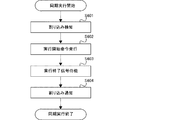
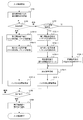
図6を用いて実行制御部510の制御シーケンスを説明する。
S601にてCPUからの画像処理開始の割り込みを待ち、検知するとS602に遷移する。
S602では入力制御部520と出力制御部530とに実行開始命令を発行し、S603に遷移する。
S603では入力側制御部520と出力側制御部530からの実行終了信号を待機し、両方の信号を受信したらS604に遷移する。
S604では入出力制御を終了し、CPU111に画像処理終了の割り込みを通知する。
A control sequence of the
In step S601, the CPU waits for an interruption of image processing start from the CPU, and if detected, the process proceeds to step S602.
In S602, an execution start command is issued to the
In S603, it waits for the execution end signal from the input
In step S604, the input / output control is ended, and the CPU 111 is notified of an interruption for the end of image processing.
(入力制御部)
入力制御部520は、画像入力部321のDMA受信部411及びパケット送信部412の同期制御と、中間バッファ342の管理とを行うモジュールである。DMA受信部411への実行開始命令は信号521にて送信し、DMA受信部からの実行終了を信号522にて受信する。パケット送信部412への実行開始命令は信号523にて送信し、パケット送信部からの実行終了は信号524にて受信する。
(Input control unit)
The
他の中間バッファ制御部330と中間バッファ342を共有する場合には、信号5111にて中間バッファを共有するように設定がなされ、信号525にて送信する同期信号と、信号526にて受信する同期信号とを用いて同期制御を行う。
同時に、バッファ状態情報を書込状態にする更新情報を信号527にて他の中間バッファ制御部330へ送信し、バッファ状態情報を読出状態にする更新情報を信号528bにて他の中間バッファ制御部330から受信することでバッファ状態情報の同期も行う。
また、パケット送信部412で画像データやバンド領域の送信が完了した場合には、入力制御部520の実行を終了させるための信号を信号529にて受信する。
When sharing the intermediate buffer 342 with another intermediate
At the same time, update information for setting the buffer state information to the write state is transmitted to another intermediate
When the
図7にて入力制御部の制御シーケンスを説明する。
S701にて実行制御部510から実行開始命令515を待ち、受信するとS702に遷移する。
S702にて他の中間バッファ制御部と中間バッファを共有しない設定であればS703−0に遷移し、共有する設定であればS710に遷移する。
S703−0では入力制御部520のバッファ状態保持部520bに保持されているバッファの状態情報を参照して、
空であれば信号521からDMA受信部411に対して実行開始命令を発行し、
フルであれば信号523からパケット送信部412に対して実行開始命令を発行し、S704−0に遷移する。
S704−0では実行開始命令を発行したモジュールからの実行終了通知を信号522、524で受信するまで待機し、終了信号を検知したら、S707−0に遷移する。
S707−0では、実行開始命令を発行したモジュールが用いた、バッファ状態保持部520bに保持されているバッファ状態情報を更新する。DMA受信部411がバッファを更新した場合はバッファ状態情報の書込状態信号528をアサートしてバッファ状態保持部520bに保持されているバッファ状態情報をフルとする。パケット送信部412がバッファを更新した場合は読出状態信号527をアサートしてバッファ状態保持部520bに保持されているバッファ状態情報を空にする。そして、バッファ状態情報を更新したら、S708に遷移する。
S708では、画像入力部321からの処理終了信号529が送信されていなかったらS702に遷移し、送信されていたらS709に遷移する。
The control sequence of the input control unit will be described with reference to FIG.
In S701, the process waits for the
In S702, if the setting does not share the intermediate buffer with another intermediate buffer control unit, the process proceeds to S703-0, and if the setting is shared, the process proceeds to S710.
In S703-0, referring to the buffer status information held in the buffer
If it is empty, an execution start command is issued from the
If it is full, an execution start command is issued from the
In S704-0, the process waits until receiving an end-of-execution notification from the module that has issued the execution start instruction using the
In S707-0, the buffer status information held in the buffer
In S708, if the
ここでS710に遷移した場合の説明に戻り、S710に遷移した場合は、入力制御部520のバッファ状態保持部520bに保持されているバッファ状態情報を参照し、フルであればS703−1に遷移し、空であればS705−2に遷移する。
S703−1に遷移した場合、入力制御部520はパケット送信部412に対して信号523から実行開始命令を発行し、S704−1に遷移する。
S704−1ではパケット送信部412の実行終了信号を信号524で受信するまで待機し、終了信号を検知したらS705−1に遷移する。
S705−1では他の中間バッファ制御部330との同期信号525とバッファの読出状態信号527をアサートし、S706−1に遷移する。
Returning to the description of the transition to S710, when transitioning to S710, the buffer state information held in the buffer
When the process proceeds to S703-1, the
In S704-1, it waits until the execution end signal of the
In S705-1, the
ここで、S705−2に遷移した場合の説明に戻り、S705−2に遷移した場合、他の中間バッファ制御部330との同期信号525をアサートし、バッファの読出状態信号527をネゲートし、S706−1に遷移する。
Returning to the description of the transition to S705-2, when transitioning to S705-2, the
S706−1では他の中間バッファ制御部333からの同期信号526を待ち、受信した場合はS707−1に遷移する。
S707−1では入力同期部520aが発行した読出状態信号527と、他の中間バッファ制御部330から発行された書込状態信号528のうちアサートされている信号を用いてバッファ状態保持部520bに保持されているバッファ状態情報を更新する。バッファ状態情報を更新したらS708に遷移する。
S708では実行制御部510に信号516から実行完了通知を行い、入力制御を終了する。
In step S706-1, the process waits for the
In S707-1, the buffer
In S708, the
(出力制御部)
出力制御部530は、画像出力部322のDMA送信部421及びパケット受信部422の同期制御と中間バッファの管理とを行うモジュールである。DMA送信部421への実行開始命令は信号531にて送信し、DMA送信部421からの実行終了を信号532にて受信する。パケット受信部422への実行開始命令は信号533にて送信し、パケット受信部422からの実行終了は信号534にて受信する。他の中間バッファ制御部330と中間バッファ342を共有する場合には、信号5112にて中間バッファを共有するように設定がなされ、信号536にて送信する同期信号と、信号535にて受信する同期信号を用いて同期制御を行う。
(Output control unit)
The
同時に、バッファ状態情報を書込状態にする更新情報を信号538にて送信し、バッファ状態情報を読出状態にする更新情報を信号537aにて受信することでバッファ状態保持部530bに保持されているバッファ状態情報の同期も行う。また、パケット受信部422で画像データやバンド領域の受信が完了した場合には出力制御部530の実行を終了させるための信号を信号539にて受信する。この信号は他の中間バッファ制御部330と中間バッファ342を共有する場合には、他の中間バッファ制御部330の画像入力部529bの終了信号を選択して用いる。
At the same time, update information that sets the buffer state information to the write state is transmitted by the
図8を用いて出力制御部530の制御シーケンスを説明する。
S801にて実行制御部510から実行開始命令517を待ち、受信するとS802に遷移する。
S802にて他の中間バッファ制御部330と中間バッファ342を共有しない設定であればS803−0に遷移し、共有する設定であればS810に遷移する。
A control sequence of the
In step S801, the process waits for an
If the setting is not to share the intermediate buffer 342 with the other intermediate
S803−0では出力制御部530のバッファ状態保持部530bに保持されているバッファの状態情報を参照し、
空であればパケット受信部422に対して信号533から実行開始命令を発行し、
フルであればDMA送信部421に対して信号531から実行開始命令を発行し、S804−0に遷移する。
In S803-0, referring to the buffer status information held in the buffer
If it is empty, an execution start command is issued from the
If it is full, an execution start command is issued from the
S804−0では実行開始命令を発行したモジュールからの実行終了信号を信号532、534から受信するまで待機し、終了信号を検知したら、S807−0に遷移する。
In S804-0, it waits until it receives from the
S807−0では、実行開始命令を発行したモジュールが用いた、バッファ状態保持部530bに保持されているバッファ状態情報を更新する。
パケット受信部422がバッファを更新した場合は、書込状態信号538をアサートして、バッファ状態保持部530bに保持されているバッファ状態情報をフルとする。DMA送信部421がバッファを更新した場合は、読出状態信号537aをアサートしてバッファ状態保持部530bに保持されているバッファ状態情報を空にする。
そして、バッファ状態保持部530bに保持されているバッファ状態情報を更新したら、S808に遷移する。
In S807-0, the buffer status information held in the buffer
When the
When the buffer status information held in the buffer
S808では、パケット受信部422からの処理終了信号539aが送信されていなかったらS802に遷移し、送信されていたらS809に遷移する。
In S808, if the
ここでS810に遷移した場合の説明に戻り、S810に遷移した場合は、出力制御部530のバッファ状態保持部530bに保持されているバッファ状態情報を参照し、空であればS803−1に遷移し、フルであればS805−2に遷移する。
Returning to the description of the transition to S810, when transitioning to S810, the buffer status information held in the buffer
S803−1に遷移した場合、出力制御部530はパケット受信部422に対して信号533から実行開始命令を発行し、S804−1に遷移する。
S804−1ではパケット送信部422の実行終了信号を信号534で受信するまで待機し、終了信号を検知したらS805−1に遷移する。
S805−1では他の中間バッファ制御部330との同期信号536とバッファの書込状態信号538をアサートし、S806−1に遷移する。
When the process proceeds to S803-1, the
In step S804-1, the process waits until the execution end signal of the
In S805-1, the
ここで、S805−2に遷移した場合の説明に戻り、S805−2に遷移した場合、他の中間バッファ制御部330との同期信号536をアサートし、バッファの書込状態信号538をネゲートし、S806−1に遷移する。
Returning to the description of the transition to S805-2, when transitioning to S805-2, the
S806−1では他の中間バッファ制御部330からの同期信号535を待ち、受信した場合はS807−1に遷移する。
S807−1では出力同期部530aが発行した書込状態信号538と、他の中間バッファ制御部330から発行された読出状態信号537のうちアサートされている信号を用いてバッファ状態保持部530bに保持されているバッファ状態情報を更新する。バッファ状態保持部530bに保持されているバッファ状態情報を更新したらS808に遷移する。
S808では実行制御部510に信号518から実行完了通知を行い、出力制御を終了する。
In step S806-1, the process waits for the
In S807-1, the buffer
In step S808, an execution completion notification is sent from the
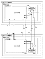
図9を用いて、スキャナ用画像処理群132の出力を中間バッファを介して、プリンタ用画像処理群133に送信する動作の例について説明する。図9はスキャナ側の出力同期部530とプリンタ側の入力同期部520がバッファを共有する場合について説明するため、図5からバッファ共有動作の説明に必要な要素を抽出した簡易的な図を示している。まず、中間バッファ制御部a320と中間バッファ制御部b330がCPU111から画像処理の実行開始の命令を受信すると、出力制御部530と入力制御部520が起動される。
An example of an operation for transmitting the output of the scanner
初めは図9Aに示すように、中間バッファ342にはデータが入っていないため、バッファ状態保持部530bに保持されているバッファ状態情報、及びバッファ状態保持部520bに保持されているバッファ状態情報は空となる。
このため、スキャナ側の出力同期部530aはパケット受信部を起動し、パケットの受信が完了したらバッファ状態情報の書込状態信号538と同期信号536をアサートする。
プリンタ側の入力同期部520aではバッファ状態保持部520bに保持されているバッファ状態情報が空のため、パケット送信部412の起動は行わずに同期信号525を出力し、他の中間バッファ制御部330からの同期信号526を待つ。
相互に同期信号が送られたら、バッファ書込状態信号538によってバッファ状態保持部530b、520bのそれぞれに保持されているバッファ状態情報をフルに切り替え、図9Bの状態で次の実行を開始する。
Initially, as shown in FIG. 9A, since the intermediate buffer 342 contains no data, the buffer status information held in the buffer
Therefore, the
Since the buffer state information held in the buffer
When the synchronization signals are sent to each other, the buffer state information held in each of the buffer
図9Bでは、バッファ状態保持部530b、520bのそれぞれに保持されているバッファ状態情報はフルであるため、スキャナ側のパケット受信部422の起動を行わずに同期信号536を出力し、他の中間バッファ制御部からの同期信号535を待つ。プリンタ側の入力同期部520ではバッファ状態保持部520bに保持されているバッファ状態情報がフルであるため、パケット送信部412を起動し、パケットの送信が完了したらバッファ状態情報の読出状態信号527と同期信号525をアサートする。相互に同期信号が送られたら、バッファ読出状態信号527によってバッファ状態保持部530b、520bのそれぞれに保持されているバッファ状態情報を空に切り替え図9Aの状態で次の実行を開始する。
以上のように、異なる中間バッファ制御部320、330でバッファの状態情報をそれぞれ同期して更新することによって、中間バッファ342を介して(DRAMを介することなく)高速なデータ転送を実現する事が出来る。
In FIG. 9B, since the buffer status information held in each of the buffer
As described above, it is possible to realize high-speed data transfer via the intermediate buffer 342 (without going through the DRAM) by synchronously updating the buffer status information in the different intermediate
<実施例2>
実施例1では、スキャナ側の画像出力部322と画像入力部331が1つの同じバッファ342にアクセスする場合を例に説明した。
実施例2では、バッファを効率的に用いて高速なデータ共有を実現するための構成について説明する。実施例2では画像出力部322と画像出力部342が2つのバッファ(例えば、342−1、342−2)に交互にアクセスするバッファ構成にし、これを同期制御する。
<Example 2>
In the first embodiment, the case where the
In the second embodiment, a configuration for realizing high-speed data sharing using a buffer efficiently will be described. In the second embodiment, the
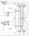
図10にて実施例2におけるバッファ構成において、バッファを共有する構成について説明する。実施例2ではバッファ状態情報を、管理するバッファの数だけ配置し、それぞれのバッファ状態情報に対して読み出し、書き出し制御信号を送信する事によって、ダブルバッファ構成を実現する。
以下で具体的な動作について図10を用いて説明する。図10に示すバッファ1状態保持部530b−1、520b−1はバッファ342−1の状態情報を保持しており、バッファ2状態保持部530b−2、520b−2はバッファ342−2の状態情報を保持している。
With reference to FIG. 10, a buffer sharing configuration in the second embodiment will be described. In the second embodiment, the buffer status information is arranged by the number of buffers to be managed, and each buffer status information is read and a write control signal is transmitted to realize a double buffer configuration.
A specific operation will be described below with reference to FIG. The
まず、中間バッファ制御部a320と中間バッファ制御部b330がCPUから画像処理の実行開始の命令を受信すると、
中間バッファ制御部a320の出力制御部530と
中間バッファ制御部b330の入力制御部520が起動される。
図10Aのように、初めは中間バッファ1、2共にデータが入っていないため、バッファ1状態保持部520b−1,バッファ2状態保持部520b−2に保持されている状態情報が共に空となる。
First, when the intermediate buffer control unit a320 and the intermediate buffer control unit b330 receive an image processing execution start command from the CPU,
The
As shown in FIG. 10A, since no data is initially stored in both the
このため、スキャナ側の出力同期部530aでは、パケット受信部422を起動し、パケットの受信が完了したらバッファ1状態情報の書込状態信号538−1と同期信号536をアサートする。
プリンタ側の入力同期部520aでは、バッファ1の状態情報が空のため、パケット送信部412の起動は行わず、同期信号525を送信し、他の中間バッファ制御部320からの同期信号526を待つ。
相互に同期信号が送られたら、バッファ書込状態信号538−1によってそれぞれのバッファ1の状態情報をフルに切り替え、図10Bの状態で次の実行を開始する。
For this reason, the
In the
When the synchronization signals are sent to each other, the buffer write state signal 538-1 switches the state information of each
図10Bでは、出力同期部はバッファ2状態保持部530b−2に保持されているバッファ2状態情報を参照する。
バッファ2状態情報は空であるため、スキャナ側のパケット受信部422を起動し、パケットの受信が完了したらバッファ2状態情報の書込状態信号538−2と同期信号536をアサートする。
プリンタ側の入力同期部520ではバッファ1状態保持部520b−1に保持されているバッファ1状態情報を参照する。バッファ1状態情報はフルであるため、パケット送信部412を起動し、パケットの送信が完了したらバッファ1状態情報の読出状態信号527−1と同期信号525をアサートする。
相互に同期信号が送られたら、バッファ1読み出し信号527−1によってバッファ1の状態情報を空にし、バッファ2の書き出し信号538−2によって、バッファ2の状態情報をフルにし、図10Cの状態で次の実行を開始する。
In FIG. 10B, the output synchronization unit refers to the
Since the
The
When the synchronization signals are sent to each other, the status information of the
図10Cでは出力同期部530はバッファ1状態保持部530b−1に保持されているバッファ1状態情報を参照する。
バッファ1状態情報は空であるため、スキャナ側のパケット受信部422を起動し、パケットの受信が完了したらバッファ1状態情報の書込状態信号と同期信号538−1をアサートする。
プリンタ側の入力同期部520ではバッファ2状態保持部520b−2に保持されているバッファ2状態情報を参照する。バッファ2状態情報はフルであるため、パケット送信部412を起動し、パケットの送信が完了したらバッファ2状態情報の読出状態信号527−2と同期信号525をアサートする。相互に同期信号が送られたら、バッファ2読み出し信号527−2によってバッファ2の状態情報を空にし、バッファ1の書込状態信号538−1によって、バッファ状態情報1をフルにし、図10Bの状態で次の実行を開始する。
In FIG. 10C, the
Since the
The
以上のように簡易な構成を追加する事で2つのバッファに交互にアクセスする構成においても、パケットの送信と受信を同時に実行する高速なデータ通信を実現する事が出来る。勿論、複数の中間バッファ制御部で共有するバッファの数は2つに限るものではない。 By adding a simple configuration as described above, even in a configuration in which two buffers are alternately accessed, high-speed data communication that simultaneously executes packet transmission and reception can be realized. Of course, the number of buffers shared by the plurality of intermediate buffer control units is not limited to two.
実施例2における並列動作の効果について説明する。
図16(a)は中間バッファが1つしかない場合(中間バッファ1のみの場合)を示し、図16(b)は中間バッファが2つある場合(中間バッファ1と2の場合)を示す。
The effect of the parallel operation in the second embodiment will be described.
FIG. 16A shows a case where there is only one intermediate buffer (in the case of only intermediate buffer 1), and FIG. 16B shows a case where there are two intermediate buffers (in the case of
図16(a)に示すように、中間バッファ1しか使用しない場合は、中間バッファ1が空の状態にならなければ出力部からの書込みは開始できない、また、中間バッファ1がフルの状態にならなければ入力部への読出しは開始できない。
As shown in FIG. 16A, when only the
具体的には、
中間バッファ1がフルの状態になり、中間バッファ1から入力部への読出しが開始され(T11)、
中間バッファ1から入力部への読出しが終了し(T12)、
中間バッファ1が空の状態になり、出力部から中間バッファ1への書込みが開始され(T13)、
中間バッファ1がフルの状態になると、中間バッファ1から入力部への読出しが開始される(T14)。
In particular,
The
Reading from the
The
When the
一方、図16(b)に示すように、中間バッファ1と中間バッファ2を使用する場合は、中間バッファ2が空の状態にならなくても、中間バッファ1が空の状態になれば、出力部から中間バッファ1への書込みは開始できる。また、中間バッファ1が空の状態にならなくても、中間バッファ2が空の状態になれば、出力部から中間バッファ2への書込みは開始できる。
中間バッファ2がフルの状態にならなくても、中間バッファ1がフルの状態になれば、中間バッファ1から入力部への読出しは開始できる。また、中間バッファ1がフルの状態にならなくても、中間バッファ2がフルの状態になれば、中間バッファ2から入力部への読出しは開始できる。
On the other hand, as shown in FIG. 16B, when the
Even if the
具体的には、
中間バッファ1がフルの状態になり、中間バッファ1から入力部への読出しが開始され(T21)、
出力部から中間バッファ2への書込みが開始され(T22)、
中間バッファ1から入力部への読出しが終了し(T23)、
中間バッファ2から入力部への読出しが開始され(T24)、
出力部から中間バッファ1への書込みが開始され(T25)、
中間バッファ2から入力部への読出しが終了し(T26)、
中間バッファ1から入力部への読出しが開始される(T27)。
In particular,
The
Writing from the output unit to the
Reading from the
Reading from the
Writing from the output unit to the
Reading from the
Reading from the
中間バッファ1と中間バッファ2を使用することによって、
中間バッファ1から入力部への読出し終了(T23)と、
中間バッファ1から入力部への読出し開始(T27)との間に、
中間バッファ2から入力部への読出しが開始し(T24)、かつ中間バッファ2から入力部への読出しが終了している(T26)。
By using
End of reading from the
Between the start of reading from the
Reading from the
同様に、
出力部から中間バッファ1への書込み終了(T21)と、
出力部から中間バッファ1への書込み開始(T25)との間に、
出力部から中間バッファ2への書込みが開始し(T22)、かつ出力部から中間バッファ2への書込みが終了している(T24)。
Similarly,
End of writing from the output unit to the intermediate buffer 1 (T21),
Between the start of writing to the
Writing from the output unit to the
前記のように、出力部が、中間バッファ1と中間バッファ2を交互に使用し、かつ入力部も、中間バッファ1と中間バッファ2を交互に使用することによって、高速なデータ通信が可能となる。
As described above, the output unit uses the
<実施例3>
実施例1ではスキャン処理とプリント処理を連続して実行する場合における中間バッファ342の共有方法について説明した。実施例3では、画像データに対してスキャン用画像処理回路群132やプリンタ用画像処理回路群133に含まれる画像処理機能を複数回適用する場合について説明する。
<Example 3>
In the first embodiment, the sharing method of the intermediate buffer 342 in the case where the scan process and the print process are continuously executed has been described. In the third embodiment, a case where the image processing function included in the scan image
スキャナ用画像処理回路群132では、スキャン時のノイズを低減するためのフィルタ処理を画像データに対して適用している。フィルタ処理はタップ数を大きくするほど空間周波数の低いノイズも除去する事が出来る。しかし、フィルタのタップ数が大きくなるほど回路規模も増大するため、コストとタップ数のバランスをとった構成を検討する必要があった。
In the scanner image
そこで、少ないタップ数のフィルタ処理を画像データに複数回適用する事で疑似的に多タップ数のフィルタ処理を行う事が考えられる。実施例3では中間バッファ342を効率的に用いてこの処理を実現する構成について説明する。ただし、実施例1と同様の構成である部分については説明を省く。 Therefore, it is conceivable to apply a filter process with a large number of taps in a pseudo manner by applying a filter process with a small number of taps to image data a plurality of times. In the third embodiment, a configuration for realizing this processing using the intermediate buffer 342 efficiently will be described. However, description of portions having the same configuration as in the first embodiment will be omitted.
図11は実施例3における同期実行部323の構成を示した図である。図5で示した実施例1における同期実行部323の構成と同等の部分については同じ番号で示し、説明を省く。図11の同期実行部323には実施例1の同期実行部323の構成に加えて状態情報交換部540を備えている。状態情報交換部540は入力制御部520のバッファ状態情報520bと、出力制御部530のバッファ状態情報530bを交換するモジュールである。
FIG. 11 is a diagram illustrating the configuration of the
具体的には、状態情報交換部540は実行制御部510から状態情報交換命令を信号541から受け取ると、入力制御部520のバッファ状態情報520bと出力制御部530のバッファ状態情報530bを入れ替える制御を行う。バッファ状態情報の交換を完了したら実行制御部510に対して信号541から完了を通知する。
Specifically, when the state
ここで、図12を用いて、実行制御部510の制御シーケンスについて説明する。
S1201にて実行制御部510はフィルタ処理を実行する回数をループ回数としてCPU111から設定され、画像処理実行開始の割り込み信号519を待つ。割り込みを検知したらS1202に遷移する。
S1202ではCPU111から指定された回数の実行開始命令を発行しているかどうか判定し、実行済みもしくはループ実行が不要であればS1203−1に遷移し、指定された回数の実行をしていない場合はS1203−0に遷移する。
Here, the control sequence of the
In step S1201, the
In S1202, it is determined whether or not the CPU 111 has issued a specified number of execution start instructions. If it has been executed or if loop execution is unnecessary, the process proceeds to S1203-1, and if the specified number of times has not been executed, The process proceeds to S1203-0.
S1203−0ではループ実行の初回であれば入力側で中間バッファを共有するように設定し、出力側で中間バッファを共有しないように設定する。ループ実行初回以降であれば入力側、出力側ともに中間バッファを共有しないように設定しS1204−0に遷移する。
S1204−0では入力制御部520と出力制御部530に実行開始命令を発行し、S1205−0に遷移する。
In step S1203-0, if the loop execution is the first time, the input side is set to share the intermediate buffer, and the output side is set not to share the intermediate buffer. If it is after the first loop execution, the input side and the output side are set not to share the intermediate buffer, and the process proceeds to S1204-0.
In S1204-0, an execution start command is issued to the
S1205−0では入力側制御部520と出力側制御部530からの実行終了信号を待機し、両方の信号を受信したらS1206に遷移する。
S1206では状態情報交換部540にバッファ状態情報の交換を命令すると同時に、画像入力部321と画像出力部322がどの利用するバッファを利用するかといった設定についても交換する。交換が完了したらS1202に遷移する。
In step S1205-0, the process waits for execution end signals from the input-
In step S1206, the status
ここで、S1202にてS1203−1に遷移した場合について説明する。
S1203−1では入力側で中間バッファを共有しないように設定し、出力側で中間バッファを共有するように設定しS1204−1に遷移する。
S1204−1はS1204−0と同様で、S1205−1とS1205−0も同様の制御を行いS1207に遷移する。
S1207ではCPU111に画像処理終了の割り込みを通知する。
Here, the case where the process proceeds to S1203-1 in S1202 will be described.
In S1203-1, the input side is set not to share the intermediate buffer, and the output side is set to share the intermediate buffer, and the process proceeds to S1204-1.
S1204-1 is the same as S1204-0, and S1205-1 and S1205-0 perform the same control and shift to S1207.
In step S <b> 1207, the CPU 111 is notified of an image processing end interrupt.
次に、図13を用いて、入力制御部520の制御シーケンスについて説明する。
S1301にて実行制御部510から実行開始命令515を待ち、受信するとS1302に遷移する。
S1302にてループ実行の初回またはループ処理をしない場合であればS1303−0に遷移し、2回目〜最終回のループ実行であればS1310に遷移する。
S1303−0では入力共有設定を参照して、中間バッファ342を共有するように設定されていればS1310に、共有しないように設定されていればS1304−0に遷移する。
S1304−0、S1310以降は図7のS703−0とS710と同様の制御であるため説明を省略する。
Next, the control sequence of the
In S1301, the
If it is determined in S1302 that loop execution is not performed for the first time or loop processing, the process proceeds to S1303-0, and if loop execution is performed for the second time to the last time, the process proceeds to S1310.
In S1303-0, referring to the input sharing setting, if the setting is made so that the intermediate buffer 342 is shared, the process proceeds to S1310, and if the setting is set not to share, the process proceeds to S1304-0.
Since steps S1304-0 and S1310 are the same as those in steps S703-0 and S710 in FIG.
次に、図14を用いて、出力制御部530の制御シーケンスについて説明する。
S1401にて実行制御部510から実行開始命令517を待ち、受信するとS1402に遷移する。
S1402にてループ処理をしない、またはループ処理の最終回を実行する場合はS1403に遷移し、ループ処理の初回〜最終回の1つ手前を実行する場合はS1410遷移する。
S1403では出力共有設定を参照して、中間バッファを共有するように設定されていればS1404−1に、共有しないように設定されていればS1410に遷移する。
S1404−0、S14010以降は図8のS803−0とS810と同様の制御であるため説明を省略する。
以上のように構成することで中間バッファを効率的に利用しつつ、画像データに対して同様の画像処理を複数回適用する事が出来る。
<その他の実施例>
本発明は、上述した実施形態の機能を実現するソフトウェアのコンピュータプログラムコードを記録した記憶媒体を、システム或いは装置に供給することによっても実現できる。この場合、そのシステム或いは装置のコンピュータ(又はCPUやMPU)が読み取り可能に記憶媒体に格納されたコンピュータプログラムコードを読み出し実行することにより、上述した実施形態の機能を実現する。
Next, the control sequence of the
In step S1401, the
If the loop process is not performed in S1402 or if the final loop process is executed, the process proceeds to S1403. If the loop process is executed immediately before the first to the last process, the process proceeds to S1410.
In S1403, with reference to the output sharing setting, if the setting is made so that the intermediate buffer is shared, the process proceeds to S1404-1, and if the setting is set not to share, the process proceeds to S1410.
Since S1404-0 and S14010 and after are the same controls as S803-0 and S810 in FIG.
With the configuration described above, the same image processing can be applied to image data a plurality of times while efficiently using the intermediate buffer.
<Other examples>
The present invention can also be realized by supplying a storage medium storing a computer program code of software that implements the functions of the above-described embodiments to a system or apparatus. In this case, the function of the above-described embodiment is realized by reading and executing the computer program code stored in the storage medium so as to be readable by the computer (or CPU or MPU) of the system or apparatus.
100 画像処理装置
110 システム制御部
120 スキャナ制御部
130 画像処理部
140 プリンタ制御部
310 DMAコントローラ
320 中間バッファ制御部a
321 画像入力部
322 画像出力部
323 同期実行部
100
321
Claims (6)
前記中間バッファ制御手段は、
DRAMから中間バッファへのデータ転送および前記中間バッファからデータ処理手段へのデータ転送を制御する入力手段と、
前記データ処理手段から前記中間バッファへのデータ転送および前記中間バッファから前記DRAMへのデータ転送を制御する出力手段と、
前記入力手段および前記出力手段のバッファ状態情報を各々保持し、前記バッファ状態情報に応じて、前記入力手段および前記出力手段の動作を制御する同期実行手段とを備え、
前記同期実行手段は、
前記入力手段から実行完了通知を受け取ると、前記入力手段のバッファ状態情報を書込状態と設定し、
前記出力手段から実行完了通知を受け取ると、前記出力手段のバッファ状態情報を読出状態と設定し、
他の中間バッファ制御手段と中間バッファを共有する場合には、該他の中間バッファ制御手段の同期実行手段とバッファ状態情報を相互に送信し、
他の中間バッファ制御手段と中間バッファを共有しない場合には、前記入力手段のバッファ状態情報と前記出力手段のバッファ状態情報を相互に送信し、
同期信号によってそれぞれの同期実行手段のバッファ状態情報を更新する
ことを特徴とするデータ制御装置。 A data control device comprising a plurality of intermediate buffer control means,
The intermediate buffer control means includes
Input means for controlling data transfer from the DRAM to the intermediate buffer and data transfer from the intermediate buffer to the data processing means;
Output means for controlling data transfer from the data processing means to the intermediate buffer and data transfer from the intermediate buffer to the DRAM;
Synchronization holding means for holding buffer status information of the input means and the output means, respectively, and controlling operations of the input means and the output means according to the buffer status information,
The synchronization execution means includes
When the execution completion notification is received from the input means, the buffer status information of the input means is set to the write state,
When the execution completion notification is received from the output means, the buffer status information of the output means is set as a read state,
When the intermediate buffer is shared with other intermediate buffer control means, the synchronization execution means of the other intermediate buffer control means and the buffer status information are mutually transmitted,
When the intermediate buffer is not shared with other intermediate buffer control means, the buffer status information of the input means and the buffer status information of the output means are sent to each other,
A data control apparatus for updating buffer status information of each synchronization execution means by a synchronization signal.
前記出力手段は、前記データ処理手段から前記中間バッファ制御手段へデータ転送する際、前記転送開始信号を受信してから前記転送終了信号を受信するまでの間に転送したデータ量から、受信データ量を算出して、前記受信データ量を前記同期実行手段に送信し、
前記同期実行手段は、前記受信データ量に基づいて、前記入力手段がアクセスするDRAM上のアドレスを算出する
ことを特徴とする請求項1に記載のデータ制御装置。 When the data is transferred from the intermediate buffer to the data processing unit, the input unit adds a transfer start signal to the data at the start of transfer and transfers the data to the data processing unit. When the transfer of a predetermined amount of data is completed, the transfer ends. Adding a signal to the data and transferring it to the data processing means;
The output means, when transferring data from the data processing means to the intermediate buffer control means, receives a received data amount from a data amount transferred between receiving the transfer start signal and receiving the transfer end signal. Calculating the received data amount to the synchronization execution means,
The data control apparatus according to claim 1, wherein the synchronization execution unit calculates an address on a DRAM accessed by the input unit based on the received data amount.
前記第2の中間バッファ制御手段の同期実行手段は、前記第1の中間バッファ制御手段の出力手段が算出した前記受信データ量に基づいて、前記第2の中間バッファ制御手段の入力手段がアクセスするDRAM上のアドレスを算出する
ことを特徴とする請求項2に記載のデータ制御装置。 The first intermediate buffer control means shares the intermediate buffer with the second intermediate buffer control means;
The synchronization execution means of the second intermediate buffer control means is accessed by the input means of the second intermediate buffer control means based on the received data amount calculated by the output means of the first intermediate buffer control means. 3. The data control apparatus according to claim 2, wherein an address on the DRAM is calculated.
前記画像データの転送開始時には前記画像データに転送開始信号とラインスタート信号が付加され、
前記画像データの転送終了時には前記画像データに転送終了信号とラインエンド信号が付加され、
前記画像データの副走査方向における1画素目のデータ転送が行われる際にはラインスタート信号が付加され、
前記画像データの副走査方向における最終画素のデータ転送が行われる際にはラインエンド信号が付加されて、前記データ処理部に転送され、
前記出力手段は前記データ処理手段から転送されるデータに付加された前記ラインスタート信号を検知してから前記ラインエンド信号を検知するまでの画素数を前記受信データ量とする
ことを特徴とする請求項2又は3に記載のデータ制御装置。 As the amount of data transferred by the input means, the number of pixels in the main scanning direction and the number of pixels in the sub-scanning direction of the image data are set,
At the start of transfer of the image data, a transfer start signal and a line start signal are added to the image data,
At the end of the transfer of the image data, a transfer end signal and a line end signal are added to the image data,
When data transfer of the first pixel in the sub-scanning direction of the image data is performed, a line start signal is added,
When data transfer of the final pixel in the sub-scanning direction of the image data is performed, a line end signal is added and transferred to the data processing unit,
The output means uses the number of pixels from detection of the line start signal added to data transferred from the data processing means to detection of the line end signal as the received data amount. Item 4. The data control device according to Item 2 or 3.
前記第1の中間バッファ制御手段が第1のデータ処理手段に関わるデータ転送を制御し、
前記第2の中間バッファ制御手段が第2のデータ処理手段に関わるデータ転送を制御する
ことを特徴とする請求項3又は4に記載のデータ制御装置。 A first data processing unit related to scan processing and a second data processing unit related to print processing;
The first intermediate buffer control means controls data transfer related to the first data processing means;
5. The data control apparatus according to claim 3, wherein the second intermediate buffer control unit controls data transfer related to the second data processing unit.
前記中間バッファ制御手段は、
DRAMから中間バッファへのデータ転送および前記中間バッファからデータ処理手段へのデータ転送を制御する入力手段と、
前記データ処理手段から前記中間バッファへのデータ転送および前記中間バッファから前記DRAMへのデータ転送を制御する出力手段と、
前記入力手段および前記出力手段のバッファ状態情報を各々保持し、前記バッファ状態情報に応じて、前記入力手段および前記出力手段の動作を制御する同期実行手段とを備え、
前記同期実行手段は、
前記入力手段から実行完了通知を受け取ると、前記入力手段のバッファ状態情報を書込状態と設定し、
前記出力手段から実行完了通知を受け取ると、前記出力手段のバッファ状態情報を読出状態と設定し、
他の中間バッファ制御手段と中間バッファを共有する場合には、該他の中間バッファ制御手段の同期実行手段とバッファ状態情報を相互に送信し、
他の中間バッファ制御手段と中間バッファを共有しない場合には、前記入力手段のバッファ状態情報と前記出力手段のバッファ状態情報を相互に送信し、
同期信号によってそれぞれの同期実行手段のバッファ状態情報を更新する
ことを特徴とするデータ制御方法。 A control method of a data control device comprising a plurality of intermediate buffer control means,
The intermediate buffer control means includes
Input means for controlling data transfer from the DRAM to the intermediate buffer and data transfer from the intermediate buffer to the data processing means;
Output means for controlling data transfer from the data processing means to the intermediate buffer and data transfer from the intermediate buffer to the DRAM;
Synchronization holding means for holding buffer status information of the input means and the output means, respectively, and controlling operations of the input means and the output means according to the buffer status information,
The synchronization execution means includes
When the execution completion notification is received from the input means, the buffer status information of the input means is set to the write state,
When the execution completion notification is received from the output means, the buffer status information of the output means is set as a read state,
When the intermediate buffer is shared with other intermediate buffer control means, the synchronization execution means of the other intermediate buffer control means and the buffer status information are mutually transmitted,
When the intermediate buffer is not shared with other intermediate buffer control means, the buffer status information of the input means and the buffer status information of the output means are sent to each other,
A data control method characterized by updating buffer status information of each synchronization execution means by a synchronization signal.
Priority Applications (1)
| Application Number | Priority Date | Filing Date | Title |
|---|---|---|---|
| JP2015130617A JP6548483B2 (en) | 2015-06-30 | 2015-06-30 | Data control apparatus and control method sharing buffer by plural data processing units |
Applications Claiming Priority (1)
| Application Number | Priority Date | Filing Date | Title |
|---|---|---|---|
| JP2015130617A JP6548483B2 (en) | 2015-06-30 | 2015-06-30 | Data control apparatus and control method sharing buffer by plural data processing units |
Publications (2)
| Publication Number | Publication Date |
|---|---|
| JP2017016285A true JP2017016285A (en) | 2017-01-19 |
| JP6548483B2 JP6548483B2 (en) | 2019-07-24 |
Family
ID=57830576
Family Applications (1)
| Application Number | Title | Priority Date | Filing Date |
|---|---|---|---|
| JP2015130617A Active JP6548483B2 (en) | 2015-06-30 | 2015-06-30 | Data control apparatus and control method sharing buffer by plural data processing units |
Country Status (1)
| Country | Link |
|---|---|
| JP (1) | JP6548483B2 (en) |
Cited By (3)
| Publication number | Priority date | Publication date | Assignee | Title |
|---|---|---|---|---|
| WO2019188233A1 (en) * | 2018-03-30 | 2019-10-03 | 日立オートモティブシステムズ株式会社 | Processing device |
| WO2020033149A1 (en) * | 2018-08-08 | 2020-02-13 | Micron Technology, Inc. | Buffer management in memory systems for read and write requests |
| US10782916B2 (en) | 2018-08-08 | 2020-09-22 | Micron Technology, Inc. | Proactive return of write credits in a memory system |
Citations (2)
| Publication number | Priority date | Publication date | Assignee | Title |
|---|---|---|---|---|
| JP3378270B2 (en) * | 1992-06-29 | 2003-02-17 | 株式会社東芝 | Multiprocessor system |
| JP4719655B2 (en) * | 2005-09-27 | 2011-07-06 | 株式会社ソニー・コンピュータエンタテインメント | Processor control technology on the network |
-
2015
- 2015-06-30 JP JP2015130617A patent/JP6548483B2/en active Active
Patent Citations (2)
| Publication number | Priority date | Publication date | Assignee | Title |
|---|---|---|---|---|
| JP3378270B2 (en) * | 1992-06-29 | 2003-02-17 | 株式会社東芝 | Multiprocessor system |
| JP4719655B2 (en) * | 2005-09-27 | 2011-07-06 | 株式会社ソニー・コンピュータエンタテインメント | Processor control technology on the network |
Cited By (10)
| Publication number | Priority date | Publication date | Assignee | Title |
|---|---|---|---|---|
| WO2019188233A1 (en) * | 2018-03-30 | 2019-10-03 | 日立オートモティブシステムズ株式会社 | Processing device |
| JP2019179309A (en) * | 2018-03-30 | 2019-10-17 | 日立オートモティブシステムズ株式会社 | Processor |
| CN111886588A (en) * | 2018-03-30 | 2020-11-03 | 日立汽车系统株式会社 | Processing apparatus |
| JP7042138B2 (en) | 2018-03-30 | 2022-03-25 | 日立Astemo株式会社 | Processing equipment |
| US11768721B2 (en) | 2018-03-30 | 2023-09-26 | Hitachi Astemo, Ltd. | Processing device |
| WO2020033149A1 (en) * | 2018-08-08 | 2020-02-13 | Micron Technology, Inc. | Buffer management in memory systems for read and write requests |
| US10782916B2 (en) | 2018-08-08 | 2020-09-22 | Micron Technology, Inc. | Proactive return of write credits in a memory system |
| US11409436B2 (en) | 2018-08-08 | 2022-08-09 | Micron Technology, Inc. | Buffer management in memory systems for read and write requests |
| US11573700B2 (en) | 2018-08-08 | 2023-02-07 | Micron Technology, Inc. | Buffer management in memory systems for read and write requests |
| US11650755B2 (en) | 2018-08-08 | 2023-05-16 | Micron Technology, Inc. | Proactive return of write credits in a memory system |
Also Published As
| Publication number | Publication date |
|---|---|
| JP6548483B2 (en) | 2019-07-24 |
Similar Documents
| Publication | Publication Date | Title |
|---|---|---|
| CN105915780B (en) | Image signal processor and apparatus including the same | |
| US6384832B1 (en) | Image processing apparatus and image processing system using the apparatus | |
| US8707132B2 (en) | Information processing apparatus, information processing method, and storage medium | |
| US8838862B2 (en) | Data transfer device, method of transferring data, and image forming apparatus | |
| JP6548483B2 (en) | Data control apparatus and control method sharing buffer by plural data processing units | |
| JP2007199815A (en) | Memory control device and memory control method | |
| US8982398B2 (en) | Image forming apparatus that allows for a multi-operation | |
| JP2006301724A (en) | Memory controller, image processing controller and electronic equipment | |
| CN102497514B (en) | Three-channel video forwarding equipment and forwarding method | |
| JP2016031547A (en) | Signal transfer unit and method for controlling the signal transfer unit | |
| JP3328246B2 (en) | DMA transfer method and system | |
| JP2020191520A (en) | Imaging device and control method thereof | |
| JP2006094400A (en) | Image processor and image processing method | |
| JP3959407B2 (en) | Image processing apparatus and image processing system | |
| US20120144150A1 (en) | Data processing apparatus | |
| JP4292218B2 (en) | Image processing apparatus and image processing system | |
| KR100367084B1 (en) | DMA controller for the high speed image processor at real time | |
| JP2014154000A (en) | Memory control device, and control method and control program thereof | |
| JP2014130425A (en) | Image forming apparatus | |
| JP5889372B2 (en) | Information processing apparatus, information processing system, information processing method, control apparatus, and control method | |
| JP2015034891A (en) | Register setting control device | |
| JP2004066651A (en) | Printing device | |
| JP2005284580A (en) | Bus device | |
| JP2008102609A (en) | Bus bridge | |
| JP2009193337A (en) | Page memory controller |
Legal Events
| Date | Code | Title | Description |
|---|---|---|---|
| A621 | Written request for application examination |
Free format text: JAPANESE INTERMEDIATE CODE: A621 Effective date: 20180622 |
|
| A977 | Report on retrieval |
Free format text: JAPANESE INTERMEDIATE CODE: A971007 Effective date: 20190227 |
|
| A131 | Notification of reasons for refusal |
Free format text: JAPANESE INTERMEDIATE CODE: A131 Effective date: 20190312 |
|
| A521 | Request for written amendment filed |
Free format text: JAPANESE INTERMEDIATE CODE: A523 Effective date: 20190508 |
|
| TRDD | Decision of grant or rejection written | ||
| A01 | Written decision to grant a patent or to grant a registration (utility model) |
Free format text: JAPANESE INTERMEDIATE CODE: A01 Effective date: 20190528 |
|
| A61 | First payment of annual fees (during grant procedure) |
Free format text: JAPANESE INTERMEDIATE CODE: A61 Effective date: 20190625 |
|
| R151 | Written notification of patent or utility model registration |
Ref document number: 6548483 Country of ref document: JP Free format text: JAPANESE INTERMEDIATE CODE: R151 |
|
| RD03 | Notification of appointment of power of attorney |
Free format text: JAPANESE INTERMEDIATE CODE: R3D03 |