JP2017011274A - 3d electronic module comprising ball grid array package stack - Google Patents
3d electronic module comprising ball grid array package stack Download PDFInfo
- Publication number
- JP2017011274A JP2017011274A JP2016125327A JP2016125327A JP2017011274A JP 2017011274 A JP2017011274 A JP 2017011274A JP 2016125327 A JP2016125327 A JP 2016125327A JP 2016125327 A JP2016125327 A JP 2016125327A JP 2017011274 A JP2017011274 A JP 2017011274A
- Authority
- JP
- Japan
- Prior art keywords
- package
- electronic module
- dimensional electronic
- packages
- flexible
- Prior art date
- Legal status (The legal status is an assumption and is not a legal conclusion. Google has not performed a legal analysis and makes no representation as to the accuracy of the status listed.)
- Granted
Links
- 239000003822 epoxy resin Substances 0.000 claims description 9
- 229920000647 polyepoxide Polymers 0.000 claims description 9
- 239000011324 bead Substances 0.000 claims description 6
- 238000005304 joining Methods 0.000 claims description 2
- 230000001070 adhesive effect Effects 0.000 description 7
- 239000000853 adhesive Substances 0.000 description 6
- 229910000679 solder Inorganic materials 0.000 description 6
- 239000003990 capacitor Substances 0.000 description 5
- 238000000034 method Methods 0.000 description 4
- 229920005989 resin Polymers 0.000 description 4
- 239000011347 resin Substances 0.000 description 4
- 238000005476 soldering Methods 0.000 description 4
- 230000009977 dual effect Effects 0.000 description 3
- PXHVJJICTQNCMI-UHFFFAOYSA-N Nickel Chemical group [Ni] PXHVJJICTQNCMI-UHFFFAOYSA-N 0.000 description 2
- 239000004642 Polyimide Substances 0.000 description 2
- VYPSYNLAJGMNEJ-UHFFFAOYSA-N Silicium dioxide Chemical compound O=[Si]=O VYPSYNLAJGMNEJ-UHFFFAOYSA-N 0.000 description 2
- 230000001419 dependent effect Effects 0.000 description 2
- 238000005516 engineering process Methods 0.000 description 2
- 229920001721 polyimide Polymers 0.000 description 2
- 238000000926 separation method Methods 0.000 description 2
- 239000000758 substrate Substances 0.000 description 2
- 238000004026 adhesive bonding Methods 0.000 description 1
- 239000004840 adhesive resin Substances 0.000 description 1
- 229920006223 adhesive resin Polymers 0.000 description 1
- 230000002411 adverse Effects 0.000 description 1
- 238000005452 bending Methods 0.000 description 1
- 238000005266 casting Methods 0.000 description 1
- 238000005234 chemical deposition Methods 0.000 description 1
- 239000000835 fiber Substances 0.000 description 1
- 230000006870 function Effects 0.000 description 1
- 239000003365 glass fiber Substances 0.000 description 1
- PCHJSUWPFVWCPO-UHFFFAOYSA-N gold Chemical compound [Au] PCHJSUWPFVWCPO-UHFFFAOYSA-N 0.000 description 1
- 229910052737 gold Inorganic materials 0.000 description 1
- 239000010931 gold Substances 0.000 description 1
- LNEPOXFFQSENCJ-UHFFFAOYSA-N haloperidol Chemical group C1CC(O)(C=2C=CC(Cl)=CC=2)CCN1CCCC(=O)C1=CC=C(F)C=C1 LNEPOXFFQSENCJ-UHFFFAOYSA-N 0.000 description 1
- 238000003475 lamination Methods 0.000 description 1
- 238000010329 laser etching Methods 0.000 description 1
- 238000004519 manufacturing process Methods 0.000 description 1
- 239000002184 metal Substances 0.000 description 1
- 229910052751 metal Inorganic materials 0.000 description 1
- 238000001465 metallisation Methods 0.000 description 1
- 229910052759 nickel Inorganic materials 0.000 description 1
- 238000004806 packaging method and process Methods 0.000 description 1
- 229920000642 polymer Polymers 0.000 description 1
- 239000000523 sample Substances 0.000 description 1
- 239000000377 silicon dioxide Substances 0.000 description 1
Images


Classifications
-
- H—ELECTRICITY
- H05—ELECTRIC TECHNIQUES NOT OTHERWISE PROVIDED FOR
- H05K—PRINTED CIRCUITS; CASINGS OR CONSTRUCTIONAL DETAILS OF ELECTRIC APPARATUS; MANUFACTURE OF ASSEMBLAGES OF ELECTRICAL COMPONENTS
- H05K1/00—Printed circuits
- H05K1/18—Printed circuits structurally associated with non-printed electric components
-
- H—ELECTRICITY
- H01—ELECTRIC ELEMENTS
- H01L—SEMICONDUCTOR DEVICES NOT COVERED BY CLASS H10
- H01L23/00—Details of semiconductor or other solid state devices
- H01L23/52—Arrangements for conducting electric current within the device in operation from one component to another, i.e. interconnections, e.g. wires, lead frames
- H01L23/538—Arrangements for conducting electric current within the device in operation from one component to another, i.e. interconnections, e.g. wires, lead frames the interconnection structure between a plurality of semiconductor chips being formed on, or in, insulating substrates
- H01L23/5384—Conductive vias through the substrate with or without pins, e.g. buried coaxial conductors
-
- H—ELECTRICITY
- H01—ELECTRIC ELEMENTS
- H01L—SEMICONDUCTOR DEVICES NOT COVERED BY CLASS H10
- H01L23/00—Details of semiconductor or other solid state devices
- H01L23/52—Arrangements for conducting electric current within the device in operation from one component to another, i.e. interconnections, e.g. wires, lead frames
- H01L23/538—Arrangements for conducting electric current within the device in operation from one component to another, i.e. interconnections, e.g. wires, lead frames the interconnection structure between a plurality of semiconductor chips being formed on, or in, insulating substrates
- H01L23/5387—Flexible insulating substrates
-
- H—ELECTRICITY
- H01—ELECTRIC ELEMENTS
- H01L—SEMICONDUCTOR DEVICES NOT COVERED BY CLASS H10
- H01L23/00—Details of semiconductor or other solid state devices
- H01L23/52—Arrangements for conducting electric current within the device in operation from one component to another, i.e. interconnections, e.g. wires, lead frames
- H01L23/538—Arrangements for conducting electric current within the device in operation from one component to another, i.e. interconnections, e.g. wires, lead frames the interconnection structure between a plurality of semiconductor chips being formed on, or in, insulating substrates
- H01L23/5389—Arrangements for conducting electric current within the device in operation from one component to another, i.e. interconnections, e.g. wires, lead frames the interconnection structure between a plurality of semiconductor chips being formed on, or in, insulating substrates the chips being integrally enclosed by the interconnect and support structures
-
- H—ELECTRICITY
- H01—ELECTRIC ELEMENTS
- H01L—SEMICONDUCTOR DEVICES NOT COVERED BY CLASS H10
- H01L23/00—Details of semiconductor or other solid state devices
- H01L23/58—Structural electrical arrangements for semiconductor devices not otherwise provided for, e.g. in combination with batteries
- H01L23/64—Impedance arrangements
- H01L23/66—High-frequency adaptations
-
- H—ELECTRICITY
- H01—ELECTRIC ELEMENTS
- H01L—SEMICONDUCTOR DEVICES NOT COVERED BY CLASS H10
- H01L24/00—Arrangements for connecting or disconnecting semiconductor or solid-state bodies; Methods or apparatus related thereto
-
- H—ELECTRICITY
- H01—ELECTRIC ELEMENTS
- H01L—SEMICONDUCTOR DEVICES NOT COVERED BY CLASS H10
- H01L24/00—Arrangements for connecting or disconnecting semiconductor or solid-state bodies; Methods or apparatus related thereto
- H01L24/01—Means for bonding being attached to, or being formed on, the surface to be connected, e.g. chip-to-package, die-attach, "first-level" interconnects; Manufacturing methods related thereto
- H01L24/10—Bump connectors ; Manufacturing methods related thereto
- H01L24/15—Structure, shape, material or disposition of the bump connectors after the connecting process
- H01L24/16—Structure, shape, material or disposition of the bump connectors after the connecting process of an individual bump connector
-
- H—ELECTRICITY
- H01—ELECTRIC ELEMENTS
- H01L—SEMICONDUCTOR DEVICES NOT COVERED BY CLASS H10
- H01L24/00—Arrangements for connecting or disconnecting semiconductor or solid-state bodies; Methods or apparatus related thereto
- H01L24/01—Means for bonding being attached to, or being formed on, the surface to be connected, e.g. chip-to-package, die-attach, "first-level" interconnects; Manufacturing methods related thereto
- H01L24/26—Layer connectors, e.g. plate connectors, solder or adhesive layers; Manufacturing methods related thereto
- H01L24/31—Structure, shape, material or disposition of the layer connectors after the connecting process
- H01L24/32—Structure, shape, material or disposition of the layer connectors after the connecting process of an individual layer connector
-
- H—ELECTRICITY
- H01—ELECTRIC ELEMENTS
- H01L—SEMICONDUCTOR DEVICES NOT COVERED BY CLASS H10
- H01L24/00—Arrangements for connecting or disconnecting semiconductor or solid-state bodies; Methods or apparatus related thereto
- H01L24/73—Means for bonding being of different types provided for in two or more of groups H01L24/10, H01L24/18, H01L24/26, H01L24/34, H01L24/42, H01L24/50, H01L24/63, H01L24/71
-
- H—ELECTRICITY
- H01—ELECTRIC ELEMENTS
- H01L—SEMICONDUCTOR DEVICES NOT COVERED BY CLASS H10
- H01L25/00—Assemblies consisting of a plurality of individual semiconductor or other solid state devices ; Multistep manufacturing processes thereof
- H01L25/03—Assemblies consisting of a plurality of individual semiconductor or other solid state devices ; Multistep manufacturing processes thereof all the devices being of a type provided for in the same subgroup of groups H01L27/00 - H01L33/00, or in a single subclass of H10K, H10N, e.g. assemblies of rectifier diodes
- H01L25/10—Assemblies consisting of a plurality of individual semiconductor or other solid state devices ; Multistep manufacturing processes thereof all the devices being of a type provided for in the same subgroup of groups H01L27/00 - H01L33/00, or in a single subclass of H10K, H10N, e.g. assemblies of rectifier diodes the devices having separate containers
- H01L25/105—Assemblies consisting of a plurality of individual semiconductor or other solid state devices ; Multistep manufacturing processes thereof all the devices being of a type provided for in the same subgroup of groups H01L27/00 - H01L33/00, or in a single subclass of H10K, H10N, e.g. assemblies of rectifier diodes the devices having separate containers the devices being of a type provided for in group H01L27/00
-
- H—ELECTRICITY
- H05—ELECTRIC TECHNIQUES NOT OTHERWISE PROVIDED FOR
- H05K—PRINTED CIRCUITS; CASINGS OR CONSTRUCTIONAL DETAILS OF ELECTRIC APPARATUS; MANUFACTURE OF ASSEMBLAGES OF ELECTRICAL COMPONENTS
- H05K1/00—Printed circuits
- H05K1/02—Details
- H05K1/14—Structural association of two or more printed circuits
- H05K1/147—Structural association of two or more printed circuits at least one of the printed circuits being bent or folded, e.g. by using a flexible printed circuit
-
- H—ELECTRICITY
- H05—ELECTRIC TECHNIQUES NOT OTHERWISE PROVIDED FOR
- H05K—PRINTED CIRCUITS; CASINGS OR CONSTRUCTIONAL DETAILS OF ELECTRIC APPARATUS; MANUFACTURE OF ASSEMBLAGES OF ELECTRICAL COMPONENTS
- H05K1/00—Printed circuits
- H05K1/18—Printed circuits structurally associated with non-printed electric components
- H05K1/189—Printed circuits structurally associated with non-printed electric components characterised by the use of a flexible or folded printed circuit
-
- H—ELECTRICITY
- H01—ELECTRIC ELEMENTS
- H01L—SEMICONDUCTOR DEVICES NOT COVERED BY CLASS H10
- H01L2224/00—Indexing scheme for arrangements for connecting or disconnecting semiconductor or solid-state bodies and methods related thereto as covered by H01L24/00
- H01L2224/01—Means for bonding being attached to, or being formed on, the surface to be connected, e.g. chip-to-package, die-attach, "first-level" interconnects; Manufacturing methods related thereto
- H01L2224/10—Bump connectors; Manufacturing methods related thereto
- H01L2224/12—Structure, shape, material or disposition of the bump connectors prior to the connecting process
- H01L2224/13—Structure, shape, material or disposition of the bump connectors prior to the connecting process of an individual bump connector
- H01L2224/13001—Core members of the bump connector
- H01L2224/13099—Material
- H01L2224/131—Material with a principal constituent of the material being a metal or a metalloid, e.g. boron [B], silicon [Si], germanium [Ge], arsenic [As], antimony [Sb], tellurium [Te] and polonium [Po], and alloys thereof
- H01L2224/13101—Material with a principal constituent of the material being a metal or a metalloid, e.g. boron [B], silicon [Si], germanium [Ge], arsenic [As], antimony [Sb], tellurium [Te] and polonium [Po], and alloys thereof the principal constituent melting at a temperature of less than 400°C
-
- H—ELECTRICITY
- H01—ELECTRIC ELEMENTS
- H01L—SEMICONDUCTOR DEVICES NOT COVERED BY CLASS H10
- H01L2224/00—Indexing scheme for arrangements for connecting or disconnecting semiconductor or solid-state bodies and methods related thereto as covered by H01L24/00
- H01L2224/01—Means for bonding being attached to, or being formed on, the surface to be connected, e.g. chip-to-package, die-attach, "first-level" interconnects; Manufacturing methods related thereto
- H01L2224/10—Bump connectors; Manufacturing methods related thereto
- H01L2224/15—Structure, shape, material or disposition of the bump connectors after the connecting process
- H01L2224/16—Structure, shape, material or disposition of the bump connectors after the connecting process of an individual bump connector
-
- H—ELECTRICITY
- H01—ELECTRIC ELEMENTS
- H01L—SEMICONDUCTOR DEVICES NOT COVERED BY CLASS H10
- H01L2224/00—Indexing scheme for arrangements for connecting or disconnecting semiconductor or solid-state bodies and methods related thereto as covered by H01L24/00
- H01L2224/01—Means for bonding being attached to, or being formed on, the surface to be connected, e.g. chip-to-package, die-attach, "first-level" interconnects; Manufacturing methods related thereto
- H01L2224/26—Layer connectors, e.g. plate connectors, solder or adhesive layers; Manufacturing methods related thereto
- H01L2224/28—Structure, shape, material or disposition of the layer connectors prior to the connecting process
- H01L2224/29—Structure, shape, material or disposition of the layer connectors prior to the connecting process of an individual layer connector
- H01L2224/29001—Core members of the layer connector
- H01L2224/29099—Material
- H01L2224/29198—Material with a principal constituent of the material being a combination of two or more materials in the form of a matrix with a filler, i.e. being a hybrid material, e.g. segmented structures, foams
- H01L2224/29199—Material of the matrix
- H01L2224/2929—Material of the matrix with a principal constituent of the material being a polymer, e.g. polyester, phenolic based polymer, epoxy
-
- H—ELECTRICITY
- H01—ELECTRIC ELEMENTS
- H01L—SEMICONDUCTOR DEVICES NOT COVERED BY CLASS H10
- H01L2224/00—Indexing scheme for arrangements for connecting or disconnecting semiconductor or solid-state bodies and methods related thereto as covered by H01L24/00
- H01L2224/01—Means for bonding being attached to, or being formed on, the surface to be connected, e.g. chip-to-package, die-attach, "first-level" interconnects; Manufacturing methods related thereto
- H01L2224/26—Layer connectors, e.g. plate connectors, solder or adhesive layers; Manufacturing methods related thereto
- H01L2224/28—Structure, shape, material or disposition of the layer connectors prior to the connecting process
- H01L2224/29—Structure, shape, material or disposition of the layer connectors prior to the connecting process of an individual layer connector
- H01L2224/29001—Core members of the layer connector
- H01L2224/29099—Material
- H01L2224/29198—Material with a principal constituent of the material being a combination of two or more materials in the form of a matrix with a filler, i.e. being a hybrid material, e.g. segmented structures, foams
- H01L2224/29298—Fillers
- H01L2224/29299—Base material
- H01L2224/29386—Base material with a principal constituent of the material being a non metallic, non metalloid inorganic material
-
- H—ELECTRICITY
- H01—ELECTRIC ELEMENTS
- H01L—SEMICONDUCTOR DEVICES NOT COVERED BY CLASS H10
- H01L2224/00—Indexing scheme for arrangements for connecting or disconnecting semiconductor or solid-state bodies and methods related thereto as covered by H01L24/00
- H01L2224/73—Means for bonding being of different types provided for in two or more of groups H01L2224/10, H01L2224/18, H01L2224/26, H01L2224/34, H01L2224/42, H01L2224/50, H01L2224/63, H01L2224/71
- H01L2224/732—Location after the connecting process
- H01L2224/73201—Location after the connecting process on the same surface
- H01L2224/73203—Bump and layer connectors
- H01L2224/73204—Bump and layer connectors the bump connector being embedded into the layer connector
-
- H—ELECTRICITY
- H01—ELECTRIC ELEMENTS
- H01L—SEMICONDUCTOR DEVICES NOT COVERED BY CLASS H10
- H01L2224/00—Indexing scheme for arrangements for connecting or disconnecting semiconductor or solid-state bodies and methods related thereto as covered by H01L24/00
- H01L2224/73—Means for bonding being of different types provided for in two or more of groups H01L2224/10, H01L2224/18, H01L2224/26, H01L2224/34, H01L2224/42, H01L2224/50, H01L2224/63, H01L2224/71
- H01L2224/732—Location after the connecting process
- H01L2224/73251—Location after the connecting process on different surfaces
- H01L2224/73253—Bump and layer connectors
-
- H—ELECTRICITY
- H01—ELECTRIC ELEMENTS
- H01L—SEMICONDUCTOR DEVICES NOT COVERED BY CLASS H10
- H01L23/00—Details of semiconductor or other solid state devices
- H01L23/48—Arrangements for conducting electric current to or from the solid state body in operation, e.g. leads, terminal arrangements ; Selection of materials therefor
- H01L23/488—Arrangements for conducting electric current to or from the solid state body in operation, e.g. leads, terminal arrangements ; Selection of materials therefor consisting of soldered or bonded constructions
- H01L23/498—Leads, i.e. metallisations or lead-frames on insulating substrates, e.g. chip carriers
- H01L23/49811—Additional leads joined to the metallisation on the insulating substrate, e.g. pins, bumps, wires, flat leads
- H01L23/49816—Spherical bumps on the substrate for external connection, e.g. ball grid arrays [BGA]
-
- H—ELECTRICITY
- H01—ELECTRIC ELEMENTS
- H01L—SEMICONDUCTOR DEVICES NOT COVERED BY CLASS H10
- H01L24/00—Arrangements for connecting or disconnecting semiconductor or solid-state bodies; Methods or apparatus related thereto
- H01L24/01—Means for bonding being attached to, or being formed on, the surface to be connected, e.g. chip-to-package, die-attach, "first-level" interconnects; Manufacturing methods related thereto
- H01L24/10—Bump connectors ; Manufacturing methods related thereto
- H01L24/12—Structure, shape, material or disposition of the bump connectors prior to the connecting process
- H01L24/13—Structure, shape, material or disposition of the bump connectors prior to the connecting process of an individual bump connector
-
- H—ELECTRICITY
- H01—ELECTRIC ELEMENTS
- H01L—SEMICONDUCTOR DEVICES NOT COVERED BY CLASS H10
- H01L24/00—Arrangements for connecting or disconnecting semiconductor or solid-state bodies; Methods or apparatus related thereto
- H01L24/01—Means for bonding being attached to, or being formed on, the surface to be connected, e.g. chip-to-package, die-attach, "first-level" interconnects; Manufacturing methods related thereto
- H01L24/26—Layer connectors, e.g. plate connectors, solder or adhesive layers; Manufacturing methods related thereto
- H01L24/28—Structure, shape, material or disposition of the layer connectors prior to the connecting process
- H01L24/29—Structure, shape, material or disposition of the layer connectors prior to the connecting process of an individual layer connector
-
- H—ELECTRICITY
- H01—ELECTRIC ELEMENTS
- H01L—SEMICONDUCTOR DEVICES NOT COVERED BY CLASS H10
- H01L2924/00—Indexing scheme for arrangements or methods for connecting or disconnecting semiconductor or solid-state bodies as covered by H01L24/00
- H01L2924/10—Details of semiconductor or other solid state devices to be connected
- H01L2924/11—Device type
- H01L2924/14—Integrated circuits
- H01L2924/143—Digital devices
- H01L2924/1434—Memory
-
- H—ELECTRICITY
- H01—ELECTRIC ELEMENTS
- H01L—SEMICONDUCTOR DEVICES NOT COVERED BY CLASS H10
- H01L2924/00—Indexing scheme for arrangements or methods for connecting or disconnecting semiconductor or solid-state bodies as covered by H01L24/00
- H01L2924/15—Details of package parts other than the semiconductor or other solid state devices to be connected
- H01L2924/181—Encapsulation
-
- H—ELECTRICITY
- H01—ELECTRIC ELEMENTS
- H01L—SEMICONDUCTOR DEVICES NOT COVERED BY CLASS H10
- H01L2924/00—Indexing scheme for arrangements or methods for connecting or disconnecting semiconductor or solid-state bodies as covered by H01L24/00
- H01L2924/30—Technical effects
- H01L2924/35—Mechanical effects
- H01L2924/351—Thermal stress
- H01L2924/3511—Warping
Abstract
Description
高周波数で動作する素子(メモリ、プロセッサ等)が市場に出現した結果、非カプセル化チップ(ベアチップ)が使用されるようになり、新たな性能問題が生じている。ベアチップのプローブ試験は、周波数が約1GHzを超えると極めて煩雑になる。第1の問題は、これらの素子を3次元電子モジュールに積層する場合、特定のチップは最大周波数で動作可能であるのに対し、他のものは動作可能でない点である。その結果、複数のチップを含むモジュールは最大周波数で動作可能でなくなる。 As a result of the appearance of elements (memory, processors, etc.) operating at high frequencies in the market, non-encapsulated chips (bare chips) have come to be used, creating new performance problems. The bare chip probe test becomes extremely complicated when the frequency exceeds about 1 GHz. The first problem is that when these elements are stacked on a three-dimensional electronic module, certain chips can operate at the maximum frequency, while others cannot. As a result, a module including a plurality of chips cannot operate at the maximum frequency.
この問題を回避する一方法は、カプセル化チップ、すなわち自身が完全に試験済みであるパッケージに配置されたチップを用いるものである。具体的には、1個のパッケージは、チップのパッドよりも広い間隔で配置されたハンダボールの形式をなす出力端を含んでいる。例えば、
チップパッドの間隔:50〜100μm、
チップをカプセル化するボールグリッドアレイパッケージの間隔:400〜800μmである。
One way to avoid this problem is to use an encapsulated chip, ie a chip placed in a package that has been fully tested. Specifically, one package includes an output end in the form of a solder ball arranged at a wider interval than the pads of the chip. For example,
Chip pad spacing: 50-100 μm,
The distance between the ball grid array packages encapsulating the chips is 400 to 800 μm.
従って試験ソケットを用いてパッケージをこのように試験することができる。 The package can thus be tested in this way using a test socket.
この観点から、これらのパッケージに適し、且つ高周波数で動作可能な積層技術を見出す必要がある。 From this point of view, it is necessary to find a stacking technique suitable for these packages and capable of operating at a high frequency.
従って、これらの種類パッケージを積層する新規の技術を提案する。より具体的には、本発明の主題は、
− 2個の電気的に試験済の電子パッケージ、すなわち各々が当該パッケージの2個の側面を接合する、主面と称する1個の面上に少なくとも1個のカプセル化チップおよび出力ボールを含む2個の電気的に試験済の電子パッケージと、
− 互いに機械的に接続され、且つ当該2個のパッケージの間に配置された2個の柔軟回路、すなわち各々が1個のパッケージに関連付けられ、且つ
・1個の面上に、当該関連付けられたパッケージのボールと接触する第1の電気的相互接続パッド、
・自身の終端に、当該関連付けられたパッケージの側面に重ねて折り畳まれた部分、
・当該折り畳まれた部分の反対側の面上に第2の電気的相互接続パッドを含む2個の柔軟回路とを含む3次元電子モジュールである。
Therefore, a new technique for stacking these kinds of packages is proposed. More specifically, the subject of the present invention is:
Two electrically tested electronic packages, i.e. comprising at least one encapsulating chip and an output ball on one side, called the main side, each joining two sides of the package An electronically tested electronic package;
-Two flexible circuits mechanically connected to each other and arranged between the two packages, each associated with one package, and on one surface, the associated A first electrical interconnect pad in contact with the ball of the package;
A part folded over the side of the associated package at its end,
A three-dimensional electronic module comprising two flexible circuits comprising a second electrical interconnection pad on the opposite side of the folded part.
本発明の一特徴によれば、2個の柔軟回路は、当該2個の柔軟回路の間に挟まれた硬質印刷回路基板により、機械的および電気的に相互接続されている。 According to one aspect of the invention, the two flexible circuits are mechanically and electrically interconnected by a rigid printed circuit board sandwiched between the two flexible circuits.
硬質回路は、当該硬質回路に潜在的に埋め込まれた受動および/または能動素子を含んでいてよい。 The rigid circuit may include passive and / or active elements that are potentially embedded in the rigid circuit.
3次元モジュールは、好適には、柔軟回路の折り目に沿って2個の柔軟回路の間のモジュールの境界に配置されたエポキシ樹脂のビードを含んでいる。 The three-dimensional module preferably includes an epoxy resin bead disposed at the module boundary between the two flexible circuits along the fold of the flexible circuit.
2個のパッケージのうち少なくとも1個は、チップの表面が視認可能になるまで薄化される。従ってパッケージは有利な特徴として、チップの可視面上に配置されたラジエータを含んでいる。 At least one of the two packages is thinned until the surface of the chip is visible. The package thus advantageously includes a radiator disposed on the visible surface of the chip.
本発明の別の特徴によれば、2個の柔軟回路のうち少なくとも1個が他方の終端で、パッケージの第1の側面とは反対側の別の側面に重ねて折り畳まれ、柔軟回路は当該他方の終端に受動および/または能動素子を含んでいる。用語「能動素子」はベアまたはカプセル化チップを指す。 According to another feature of the invention, at least one of the two flexible circuits is folded at the other end and over another side opposite the first side of the package, It includes passive and / or active elements at the other end. The term “active device” refers to a bare or encapsulated chip.
受動および/または能動素子は典型的には1GHzよりも高い周波数で動作する。 Passive and / or active devices typically operate at frequencies above 1 GHz.
本発明はまた、3次元電子積層にも関し、上述のような複数の3次元電子モジュールを含み、当該モジュールは主面とは反対側の面により互いに接着されていることを特徴とする。 The present invention also relates to a three-dimensional electronic stack, including a plurality of three-dimensional electronic modules as described above, wherein the modules are bonded to each other by a surface opposite to the main surface.
本発明の別の主題は、上述のような相互接続印刷回路基板、および当該相互接続印刷回路基板に載置され、且つ柔軟回路の第2の電気的相互接続パッドと接触する電気的相互接続ボールを介して電気的に接続された3次元電子モジュールまたは積層を含む3次元電子装置である。 Another subject of the present invention is an interconnect printed circuit board as described above, and an electrical interconnect ball mounted on the interconnect printed circuit board and in contact with a second electrical interconnect pad of the flexible circuit A three-dimensional electronic device including a three-dimensional electronic module or a stack electrically connected via a switch.
本発明の他の特徴および利点は、添付の図面を参照しながら、非限定的な例に基づく以下の詳細説明を精査することにより明らかになろう。 Other features and advantages of the present invention will become apparent upon review of the following detailed description based on non-limiting examples with reference to the accompanying drawings.
各図面を通じて同一要素は同一参照番号により識別される。 Throughout the drawings, identical elements are identified by identical reference numerals.
以下の説明において、「高い」、「低い」、「前面」、「後面」および「側面」の用語は記述する図面の向きに関して用いられる。モジュール、積層または素子が他の向きに応じて配置されている限り、方向に関する用語は限定的ではなく例示的に示される。 In the following description, the terms “high”, “low”, “front”, “rear” and “side” are used with respect to the orientation of the drawing to be described. As long as the modules, stacks or elements are arranged according to other orientations, the directional terms are shown by way of example and not limitation.
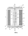
本発明による3次元電子モジュールの第1の例について図1、2を参照しながら記述する。2個のボールグリッドアレイ(BGA)パッケージが、2個の隣接する柔軟またはフレックス印刷回路基板(PCB)を含む基板の両面に載置されている。 A first example of a three-dimensional electronic module according to the present invention will be described with reference to FIGS. Two ball grid array (BGA) packages are mounted on both sides of a substrate including two adjacent flexible or flex printed circuit boards (PCBs).
ボールグリッドアレイ(BGA)パッケージ10は各々、エポキシ樹脂12にカプセル化された少なくとも1個のチップ11を含み、各チップ11は、主面15と称するパッケージの単一の面上に配置されたパッケージの出力ボール13に接続されている。長さLb、幅Ibおよび厚さebのパッケージ10は従って、共に寸法がLb×Ibである主面15および外面14と称する反対側の面、および寸法がIb×ebである側面16を有している。以下の寸法が典型的である。
− 6mm≦Lb≦9mm、
− 6mm≦Ib≦14mm、
− 0.8mm≦eb≦1.4mm
Each of the ball grid array (BGA)
− 6 mm ≦ L b ≦ 9 mm,
−6 mm ≦ I b ≦ 14 mm,
− 0.8 mm ≦ e b ≦ 1.4 mm
積層を意図されたこれらのパッケージ10は、製造業者により試験ソケットおよび適当な検査器を用いて電気的に試験され、次いで試験済パッケージとして販売される。このような試験済パッケージの製造業者のうち、Micron、Xilinx、Samsung、Freescale、Infineon、STMicroelectronics等が挙げられる。本発明による3次元モジュールはこのような試験済パッケージを含んでいる。
These
2個の試験済パッケージが以下でPCBと称する基板の対向する2面に載置される。より具体的には、PCBは2個の柔軟回路20を含んでいる。長さLf(Lf=Lf1+Lf2)、幅Ifおよび厚さefの各柔軟回路20もまた、パッケージのボール13のように分散された第1の相互接続パッド22を備えた主面21、寸法がLf×Ifである反対側の面23、および寸法がLf×efである側面を有している。以下が得られる。
Lf≧Lb+ebおよびIf=Ib
Two tested packages are mounted on two opposing sides of a substrate, hereinafter referred to as a PCB. More specifically, the PCB includes two
L f ≧ L b + e b and I f = I b
以下の寸法が典型的である。
− 7mm≦Lf≦11mm、
− 6mm≦If≦14mm、
− 0.8mm≦eb≦1.4mm
The following dimensions are typical:
− 7 mm ≦ L f ≦ 11 mm,
− 6 mm ≦ I f ≦ 14 mm,
− 0.8 mm ≦ e b ≦ 1.4 mm
フレックス回路20は一般に多層化されていて、折り畳み等の相当な変形を許すべく一般にポリイミド製であり、すなわち内部にガラス繊維を含んでいない。ポリイミドはまた、繊維で強化されていないエポキシ樹脂で代替可能である。フレックス回路20は、当該フレックス回路の主面21に配置された(且つパッケージの出力ボール13と接触させる)第1の電気的相互接続パッド22と、当該フレックス回路の部分26の反対側の面23(パッケージの側面に重ねて折り畳まれるべく意図された)に配置された寸法がLf2×Ifである第2の電気的相互接続パッド24との間で信号を誘導すべく意図された電気トラックを含み、図2では視認不可な面23にあるこれらの第2の相互接続パッド24を破線で示している。典型的には、
Lf1=Lb且つLf2≧ebである。
The
L f1 = L b and L f2 ≧ e b .
各パッケージ10は従って、以下のようにフレックス回路20に載置されている。すなわち、
− パッケージの出力ボール13およびフレックス回路の主部分27の第1の相互接続パッド22(折り畳まれない)を機械的および電気的に接触させ(例えば従来の有鉛または無鉛ハンダを用いるハンダ付けにより)、従ってフレックス回路の部分26が主部分27から突出する、
− 第2の相互接続パッド24がパッケージの前記側面16と同じ高さになるよう当該フレックス回路を90°折り曲げることにより、パッケージの側面16を当該フレックス回路の(突出)部分26と機械的に接触させる。
Each
The
The
充填樹脂17(例えばエポキシ樹脂)を従来方式でボール13の間に挿入する。
A filling resin 17 (for example, an epoxy resin) is inserted between the
これらの部分26は、パッケージの側面に接着される。この接着は、側面16に接着される部分26を完全に平坦に保てるようにするツールまたはジグを用いて実行される。接着剤30は、パッケージの側面16と折り畳まれた柔軟部分26との間のレベル調整器の役割を果たす。これはパッケージングに極めて重要であり、特に、BGAパッケージは一般に、「反り」としても知られる湾曲を示し、当該湾曲はパッケージの寸法に応じて50〜150μmに達し得る。当該湾曲は従って、ボール25の共平面性、従ってハンダ付け性能に弊害をもたらす。
These
2対のパッケージ/フレックス回路がこのように得られ、これら自身が、最終的に図1に示すように2個のパッケージ10およびPCBを用いて3次元モジュールを形成すべくフレックス回路(接着剤は図示せず)の反対側の面23を接着することにより組み立てられる。ハンダボール25が、当該3次元モジュールがユーザの印刷回路基板(またはPCB)に載置可能なように第2の相互接続パッド24に配置される。
Two pairs of package / flex circuits are thus obtained, and they themselves are flex circuits (adhesive is used to form a three-dimensional module using two
各パッケージ10は図3に示すように薄化することができる。薄化の後でチップ11の背面が視認可能になる。薄化済パッケージの外面14は、チップ11により生じた熱を逃がすために、例えば金属のラジエータ40を収納可能である。ラジエータ40は次いで、自身の断面を介してコールドプレートに接続される。ラジエータとチップ11の背面との間の熱接続41は、一般に熱接着剤を用いるか、または最適にはハンダを用いて実現される。後者の場合、外面14は、例えばニッケルと金の化学堆積を介して金属化される。この方式では、フレックス回路の部分26の長さLf2が伸びてため、第2の相互接続パッド24または間隔の数を増やすことができる。3次元モジュールは、図3に示すように各パッケージ10上にラジエータ40を含んでいても、または以下の3次元モジュールの場合で分かるように、1個のパッケージ上に単一のラジエータを含んでいて別の3次元モジュールの別のパッケージと共有されてもよい。この場合、図5a、5bのモジュール100について分かるように、長さLf2はフレックス回路毎に異なっている。
Each
図1〜3に示すように、パッケージ/フレックス回路のペアは直接組み立てられても、または図4、5に示すように、接地および電源面を含む長さLc、幅Icおよび厚さecの「コア」回路と称する中央硬質印刷回路基板50を介して組み立てられてもよく、当該回路は寸法がLc×Icの面を介して2個のフレックス回路20の部分27に機械的および電気的に接続されている。換言すれば、PCBは2個のフレックス回路20だけを含んでいても、または2個のフレックス回路20の間に「コア」回路50を含んでいてもよい。実際には、「コア」回路50が両者の間に挟まれた2個のフレックス回路20を含むPCB回路は、各パッケージ10がPCB回路のいずれかの側に載置されてパッケージから突出する2個のフレックス回路の部分26がパッケージの側面16に重ねて折り畳まれる前に製造される。
The package / flex circuit pair can be assembled directly as shown in FIGS. 1-3, or the length L c , width I c and thickness e including ground and power planes as shown in FIGS. c may be assembled via a central rigid printed
図4bに、能動および/または受動素子60を一体化すると共に、特にコンデンサを分離する一般に多層化された「コア」回路50を2個のフレックス回路20の間のPCBに含む、本発明による3次元モジュールの一例を示す。図4bにおいて、素子60を一体化している層は、一方では2個の層51の間に、他方では3個の層51の間にある。これらのコンデンサは、パッケージ10のチップ11のなるべく近くに配置されていて、最小のインダクタンスで電力を送ることができる。能動および受動素子60は「コア」回路50の厚さの範囲内に配置されており、他のレベルが次いで、PCBを製造する場合と同様に当該素子に接着される。金属化された貫通孔150は、相互接続を実現すべく「コア」および2個のフレックス回路(またはフレックス)の全て(図に示すように)または一部を通過する。
In FIG. 4b, an active and / or
図4cに見られる一代替案によれば、能動および/または受動素子60、特にコンデンサは、複数の層51を含む「コア」回路50の表面に載置されていてよく、これらの素子60は一般に極めて小型(402、すなわち1mm×0.5mm型)の素子であるため、金属化された貫通孔が「コア」回路50を通過するのに充分なスペースを残すことができる。素子60は、表面載置技術を用いてPCBに載置され、次いで、フレックス20を接着できるように接着剤を受容する平坦面を設けるべくこれらの素子60の上に樹脂151が堆積される。コンデンサ(e2)の現在の厚さは0.6mmであり、特定のサプライヤは既に0.4mm未満の厚さを提案している。載置される素子60の厚さは従って0.7mmとなって、(e3)の場合0.5mmまで減少する。全体の厚さ(e4)を1.5mm〜1.7mmとすることは充分可能である。
According to one alternative seen in FIG. 4 c, active and / or
図4aに、各パッケージ10の2個の対向する側面16に重ねて折り畳まれたフレックス回路20を備えたモジュールを示す。主な利点は機能の分離によるものである。すなわち、
− パッケージの側面16に重ねて折り畳まれ(図の最下部)、外部接続部(ボール25)を支持するフレックス。
− パッケージの側面16に重ねて折り畳まれたフレックス、当該側面は先行する面の反対側(図の最上部)にあり、それらの面23に能動および/または受動素子60(コンデンサ、抵抗等)および/または「バッファ」型能動回路が載置されていることで「コア」回路50が不要となる。
FIG. 4 a shows a module with a
A flex that is folded over the
A flex folded over the
潜在的に、2個のフレックス回路20のうち一方だけが素子60を自身の上部の折り畳まれた部分に含んでいる。
Potentially, only one of the two
受動および/または能動素子(「コア」回路に一体化または載置されているか、あるいはフレックスに載置されている)を用いる上述の方式により、3次元モジュールを、RDIMM(レジスタードデュアルインラインメモリモジュール)またはLRDIMM(負荷軽減デュアルインラインメモリモジュール)のいずれにせよ、DIMM(デュアルインラインメモリモジュール)のように電気的に自律化させることができる。 In the manner described above using passive and / or active elements (integrated or mounted in a “core” circuit or mounted in a flex), a three-dimensional module is converted into an RDIMM (registered dual in-line memory module). ) Or LRDIMM (load reducing dual in-line memory module), it can be electrically autonomous like DIMM (dual in-line memory module).
好適には、3次元モジュール100のPCBが2個のフレックス回路20の間に配置された「コア」回路50を含んでいる場合、シリカ充填エポキシ樹脂のビード70が、付随するパッケージ10の側面16に重ねて折り畳まれた際に各フレックス回路20により、形成された屈曲部の間に各々導入される。当該ビード70は従って、幅Ifにわたり広がるため、ボール25を「フレックス」回路の相互接続パッド24にハンダ付けするステップの実行中に、溶けたハンダが入り込むのを防ぐことができる。フレックス回路がパッケージの両方の側面に重ねて折り畳まれている場合、2個のビード70は図4a、5aに示すように配置される。
Preferably, if the PCB of the three-
このように得られた複数の3次元モジュール100を積層することができる。これらは典型的には、接着剤またはエポキシ樹脂1001を用いて接着される。図5a、5bに、3個のモジュール100の、従って合計6個のパッケージ10を含む積層1000を示すが、各パッケージの熱抵抗は重ね合わされたパッケージの場合のように層には依存しないため、これに限定されない。実際、各パッケージ10は、隣接パッケージに影響を受けないため、同一の熱抵抗を有している。
A plurality of three-
これらの図において、パッケージ10は薄化されていて、ラジエータ40を備えており、一部のラジエータは、特に積層1000の全厚を増やさないように隣接するモジュール100の2個のパッケージ10で共有されている。図5aにおいて、フレックス回路20は、一方に接続部(ボール25)を、他方に受動および/または能動素子60を備えた各パッケージ側面16に重ねて折り畳まれているため、「コア」回路50は不要である。図5bにおいて、フレックス回路20は、接続部(ボール25)を備えた単一のパッケージ側面16に重ねて折り畳まれていて、受動および/または能動素子は「コア」回路50に一体化されている。しかし、上述の3次元モジュールのいずれも積層されて、熱接着剤を用いて、またはハンダ付けにより互いに接着されていてよい、薄化済パッケージを備えるが側面16に対向する受動要素は無い3次元モジュールが、受動要素等を備えた非薄化済パッケージを備えた3次元モジュールに積層されていてよい。当該積層1000は無論、各フレックス回路の第2の相互接続パッド24およびこれらのパッドに配置されたハンダボール25を介してユーザの相互接続回路(図示せず)に機械的および電気的に接続されるべく意図されている。
In these figures, the
現在知られている他の全ての技術に対する当該3次元積層技術の主な利点は極めて多い。すなわち、
− モジュールの側面上にルーティングが無い、
− レベル間相互接続用のポリマー貫通孔(TPV)または金型貫通孔(TMV)が無い、
− ジグを用いて接着された構造によるボールの共平面性、
− 本質的に、積層されるパッケージの数に制限が無い、
− ユーザの相互接続PCBにおける容量性分離を、
・鋳造無し、
・モジュール面を金属化無し、
・レーザーエッチング無しに一体化可能であること。
The main advantages of the 3D stacking technology over all other currently known technologies are numerous. That is,
− No routing on the side of the module,
-No polymer through hole (TPV) or mold through hole (TMV) for interlevel interconnection,
-The co-planarity of the ball due to the structure bonded with the jig,
-Essentially, there is no limit to the number of packages that can be stacked,
-Capacitive separation in the user's interconnect PCB,
・ No casting,
・ No metallization on the module surface
-Can be integrated without laser etching.
一つの短所として、3次元モジュールの高さHが、6〜9mmの間で変動する標準BGAパッケージの長さLbに依存することに加え、折り畳まれたフレックスおよびボールの厚さefが、片側に重ねて折り畳んだ場合に約700〜800μmであることが挙げられる。 One disadvantage, the height H of the three-dimensional module, in addition to being dependent on the length L b of the standard BGA package varies between 6~9Mm, thickness e f of the folded flex and ball, It is about 700 to 800 μm when folded on one side.
当該積層方法は特に、メモリパッケージの積層に有利である。 This stacking method is particularly advantageous for stacking memory packages.
10 パッケージ
11 チップ
12 エポキシ樹脂
13 出力ボール
14 外面
15 主面
16 側面
17 充填樹脂
20 フレックス回路
21 主面
22、24 相互接続パッド
23 反対側の面
25 ボール
26、27 フレックス回路の部分
30 接着剤
40 ラジエータ
41 熱接続
50 「コア」回路
51 層
60 能動/受動素子
70 ビード
100 3次元モジュール
150 貫通孔
151 樹脂
1000 積層
1001 エポキシ樹脂
DESCRIPTION OF
Claims (9)
− 互いに機械的に接続され、且つ前記2個のパッケージの間に配置された2個の柔軟回路(20)であって、各々が1個のパッケージ(10)に関連付けられ、且つ
・1個の面(21)上に、前記関連付けられたパッケージの前記出力ボール(13)と接触する第1の電気的相互接続パッド(22)、
・自身の終端に、前記関連付けられたパッケージの側面(16)に重ねて折り畳まれた部分(26)、
・前記折り畳まれた部分(26)の反対側の面上に第2の電気的相互接続パッド(24)を含む2個の柔軟回路(20)とを含む3次元電子モジュール(100)。 -Two electrically tested electronic packages (10), at least one on one surface, called the main surface (15), each joining the two side surfaces (16) of said package Two electrically tested electronic packages (10) including one encapsulating chip (11) and an output ball (13);
Two flexible circuits (20) mechanically connected to each other and arranged between the two packages, each associated with one package (10), and A first electrical interconnection pad (22) on the surface (21) that contacts the output ball (13) of the associated package;
A portion (26) folded over the end (16) of the associated package at its end;
A three-dimensional electronic module (100) comprising two flexible circuits (20) comprising a second electrical interconnection pad (24) on the opposite side of the folded part (26).
Applications Claiming Priority (2)
| Application Number | Priority Date | Filing Date | Title |
|---|---|---|---|
| FR1555857A FR3038130B1 (en) | 2015-06-25 | 2015-06-25 | 3D ELECTRONIC MODULE COMPRISING A STACK OF BALL CASES |
| FR1555857 | 2015-06-25 |
Publications (2)
| Publication Number | Publication Date |
|---|---|
| JP2017011274A true JP2017011274A (en) | 2017-01-12 |
| JP6845627B2 JP6845627B2 (en) | 2021-03-17 |
Family
ID=54199819
Family Applications (1)
| Application Number | Title | Priority Date | Filing Date |
|---|---|---|---|
| JP2016125327A Active JP6845627B2 (en) | 2015-06-25 | 2016-06-24 | 3D electronic module containing stacking of ball grid array packages |
Country Status (5)
| Country | Link |
|---|---|
| US (1) | US10064278B2 (en) |
| EP (1) | EP3109899B1 (en) |
| JP (1) | JP6845627B2 (en) |
| FR (1) | FR3038130B1 (en) |
| TW (1) | TWI708336B (en) |
Families Citing this family (1)
| Publication number | Priority date | Publication date | Assignee | Title |
|---|---|---|---|---|
| RU190135U1 (en) * | 2019-04-16 | 2019-06-21 | Федеральное государственное автономное образовательное учреждение высшего образования "Национальный исследовательский университет "Московский институт электронной техники" | MULTI CRYSTAL MEMORY MODULE |
Family Cites Families (6)
| Publication number | Priority date | Publication date | Assignee | Title |
|---|---|---|---|---|
| US5224023A (en) * | 1992-02-10 | 1993-06-29 | Smith Gary W | Foldable electronic assembly module |
| WO2005104324A2 (en) * | 2004-04-15 | 2005-11-03 | Smith Gary W | Folded, fully buffered memory module |
| US20070211711A1 (en) * | 2006-03-08 | 2007-09-13 | Clayton James E | Thin multichip flex-module |
| US8345431B2 (en) * | 2008-01-02 | 2013-01-01 | Microelectronics Assembly Technologies, Inc. | Thin multi-chip flex module |
| US8278141B2 (en) * | 2008-06-11 | 2012-10-02 | Stats Chippac Ltd. | Integrated circuit package system with internal stacking module |
| JP2011035345A (en) * | 2009-08-06 | 2011-02-17 | Fujitsu Ltd | Semiconductor device module, electronic circuit unit, electronic device, and method of manufacturing semiconductor device module |
-
2015
- 2015-06-25 FR FR1555857A patent/FR3038130B1/en not_active Expired - Fee Related
-
2016
- 2016-06-23 US US15/190,837 patent/US10064278B2/en active Active
- 2016-06-23 EP EP16175880.0A patent/EP3109899B1/en active Active
- 2016-06-24 JP JP2016125327A patent/JP6845627B2/en active Active
- 2016-06-24 TW TW105120001A patent/TWI708336B/en active
Also Published As
| Publication number | Publication date |
|---|---|
| JP6845627B2 (en) | 2021-03-17 |
| EP3109899A1 (en) | 2016-12-28 |
| TWI708336B (en) | 2020-10-21 |
| EP3109899B1 (en) | 2020-03-25 |
| US10064278B2 (en) | 2018-08-28 |
| TW201709440A (en) | 2017-03-01 |
| US20160381799A1 (en) | 2016-12-29 |
| FR3038130B1 (en) | 2017-08-11 |
| FR3038130A1 (en) | 2016-12-30 |
Similar Documents
| Publication | Publication Date | Title |
|---|---|---|
| CN108364921B (en) | Efficient heat removal from diode-embedded component carrier | |
| US7960843B2 (en) | Chip arrangement and method of manufacturing a chip arrangement | |
| US6774473B1 (en) | Semiconductor chip module | |
| KR101904409B1 (en) | Microelectronic package with stacked microelectronic units and method for manufacture thereof | |
| US9018040B2 (en) | Power distribution for 3D semiconductor package | |
| KR101065935B1 (en) | Electronic component mounting apparatus and manufacturing method thereof | |
| KR20030071764A (en) | Carrier-based electronic module | |
| KR20060069231A (en) | Multi-level semiconductor module and method for manufacturing the same | |
| KR20060069229A (en) | Multi-level semiconductor module | |
| US20100059876A1 (en) | Electronic component package and method of manufacturing the same | |
| JP2002506289A (en) | Semiconductor device having a large number of semiconductor chips | |
| US8836102B2 (en) | Multilayered semiconductor device, printed circuit board, and method of manufacturing multilayered semiconductor device | |
| JP4074040B2 (en) | Semiconductor module | |
| JP4062066B2 (en) | Semiconductor package and stacked semiconductor package | |
| KR20080027586A (en) | Semiconductor die module and package and fabricating method of semicondctor package | |
| JP6845627B2 (en) | 3D electronic module containing stacking of ball grid array packages | |
| JP4600443B2 (en) | Semiconductor package and stacked semiconductor package | |
| US20070159204A1 (en) | Semiconductor device and electronic component module using the same | |
| US20030043650A1 (en) | Multilayered memory device | |
| KR19980058412A (en) | Multilayer Multi-chip Module Semiconductor Device and Manufacturing Method Thereof | |
| KR101046251B1 (en) | Stacked Semiconductor Packages | |
| KR20000056804A (en) | Stacked type ball grid array package | |
| US20070096333A1 (en) | Optimal stacked die organization | |
| KR100374517B1 (en) | Module structure of a power amplifier and method for packaging same | |
| KR100818077B1 (en) | Method for manufacturing bga type stack package by using alignment pin |
Legal Events
| Date | Code | Title | Description |
|---|---|---|---|
| A621 | Written request for application examination |
Free format text: JAPANESE INTERMEDIATE CODE: A621 Effective date: 20190606 |
|
| A977 | Report on retrieval |
Free format text: JAPANESE INTERMEDIATE CODE: A971007 Effective date: 20200827 |
|
| A131 | Notification of reasons for refusal |
Free format text: JAPANESE INTERMEDIATE CODE: A131 Effective date: 20200901 |
|
| A521 | Request for written amendment filed |
Free format text: JAPANESE INTERMEDIATE CODE: A523 Effective date: 20201126 |
|
| TRDD | Decision of grant or rejection written | ||
| A01 | Written decision to grant a patent or to grant a registration (utility model) |
Free format text: JAPANESE INTERMEDIATE CODE: A01 Effective date: 20210202 |
|
| A61 | First payment of annual fees (during grant procedure) |
Free format text: JAPANESE INTERMEDIATE CODE: A61 Effective date: 20210226 |
|
| R150 | Certificate of patent or registration of utility model |
Ref document number: 6845627 Country of ref document: JP Free format text: JAPANESE INTERMEDIATE CODE: R150 |
|
| R250 | Receipt of annual fees |
Free format text: JAPANESE INTERMEDIATE CODE: R250 |