JP2016518800A - Transfer function adjustment - Google Patents
Transfer function adjustment Download PDFInfo
- Publication number
- JP2016518800A JP2016518800A JP2016514420A JP2016514420A JP2016518800A JP 2016518800 A JP2016518800 A JP 2016518800A JP 2016514420 A JP2016514420 A JP 2016514420A JP 2016514420 A JP2016514420 A JP 2016514420A JP 2016518800 A JP2016518800 A JP 2016518800A
- Authority
- JP
- Japan
- Prior art keywords
- signal
- input signal
- input
- representation
- envelope
- Prior art date
- Legal status (The legal status is an assumption and is not a legal conclusion. Google has not performed a legal analysis and makes no representation as to the accuracy of the status listed.)
- Pending
Links
Images


Classifications
-
- H—ELECTRICITY
- H03—ELECTRONIC CIRCUITRY
- H03F—AMPLIFIERS
- H03F1/00—Details of amplifiers with only discharge tubes, only semiconductor devices or only unspecified devices as amplifying elements
- H03F1/02—Modifications of amplifiers to raise the efficiency, e.g. gliding Class A stages, use of an auxiliary oscillation
- H03F1/0205—Modifications of amplifiers to raise the efficiency, e.g. gliding Class A stages, use of an auxiliary oscillation in transistor amplifiers
- H03F1/0211—Modifications of amplifiers to raise the efficiency, e.g. gliding Class A stages, use of an auxiliary oscillation in transistor amplifiers with control of the supply voltage or current
- H03F1/0216—Continuous control
- H03F1/0222—Continuous control by using a signal derived from the input signal
- H03F1/0227—Continuous control by using a signal derived from the input signal using supply converters
-
- H—ELECTRICITY
- H03—ELECTRONIC CIRCUITRY
- H03F—AMPLIFIERS
- H03F3/00—Amplifiers with only discharge tubes or only semiconductor devices as amplifying elements
- H03F3/189—High frequency amplifiers, e.g. radio frequency amplifiers
- H03F3/19—High frequency amplifiers, e.g. radio frequency amplifiers with semiconductor devices only
-
- H—ELECTRICITY
- H03—ELECTRONIC CIRCUITRY
- H03F—AMPLIFIERS
- H03F3/00—Amplifiers with only discharge tubes or only semiconductor devices as amplifying elements
- H03F3/20—Power amplifiers, e.g. Class B amplifiers, Class C amplifiers
- H03F3/21—Power amplifiers, e.g. Class B amplifiers, Class C amplifiers with semiconductor devices only
-
- H—ELECTRICITY
- H04—ELECTRIC COMMUNICATION TECHNIQUE
- H04L—TRANSMISSION OF DIGITAL INFORMATION, e.g. TELEGRAPHIC COMMUNICATION
- H04L25/00—Baseband systems
- H04L25/02—Details ; arrangements for supplying electrical power along data transmission lines
- H04L25/03—Shaping networks in transmitter or receiver, e.g. adaptive shaping networks
- H04L25/03828—Arrangements for spectral shaping; Arrangements for providing signals with specified spectral properties
- H04L25/03834—Arrangements for spectral shaping; Arrangements for providing signals with specified spectral properties using pulse shaping
-
- H—ELECTRICITY
- H03—ELECTRONIC CIRCUITRY
- H03F—AMPLIFIERS
- H03F2200/00—Indexing scheme relating to amplifiers
- H03F2200/102—A non-specified detector of a signal envelope being used in an amplifying circuit
-
- H—ELECTRICITY
- H03—ELECTRONIC CIRCUITRY
- H03F—AMPLIFIERS
- H03F2200/00—Indexing scheme relating to amplifiers
- H03F2200/129—Indexing scheme relating to amplifiers there being a feedback over the complete amplifier
-
- H—ELECTRICITY
- H03—ELECTRONIC CIRCUITRY
- H03F—AMPLIFIERS
- H03F2200/00—Indexing scheme relating to amplifiers
- H03F2200/451—Indexing scheme relating to amplifiers the amplifier being a radio frequency amplifier
Landscapes
- Engineering & Computer Science (AREA)
- Power Engineering (AREA)
- Computer Networks & Wireless Communication (AREA)
- Signal Processing (AREA)
- Physics & Mathematics (AREA)
- Spectroscopy & Molecular Physics (AREA)
- Amplifiers (AREA)
- Tone Control, Compression And Expansion, Limiting Amplitude (AREA)
- Control Of Amplification And Gain Control (AREA)
Abstract
本発明は、エンベロープ追跡増幅段において制御するための技法に関し、これは、増幅器の出力信号の表現を決定することと、増幅器の入力信号の表現を決定することと、増幅器のターゲット特性に従って入力信号の決定された表現を調整することと、調整された入力と、出力の決定された表現とを比較することと、比較に依存して制御信号を生成することとを備える。【選択図】図3The present invention relates to a technique for controlling in an envelope tracking amplification stage, which determines a representation of an amplifier output signal, a representation of an amplifier input signal, and an input signal according to the target characteristics of the amplifier. Adjusting the determined representation of the output, comparing the adjusted input with the determined representation of the output, and generating a control signal dependent on the comparison. [Selection] Figure 3
Description
本発明は、エンベロープ追跡電力増幅器に関する。 The present invention relates to an envelope tracking power amplifier.
エンベロープ追跡電力増幅器アーキテクチャは周知であり、そのようなものの一例が図1に示される。 Envelope tracking power amplifier architectures are well known and an example of such is shown in FIG.
図1では、入力信号がライン22上で供給される。入力信号は、電力増幅器18の入力に伝達される前に送信機RF変調器ブロック20に供給される。電力増幅器18は、入力信号のRF増幅バージョンをライン24上でRF出力信号として供給する。送信機RF変調器ブロック20は、入力信号を変調し、入力信号をRF信号へと変換もする。
In FIG. 1, an input signal is provided on
ライン22上の入力信号はまた、AM(振幅変調)ブロック12に入力として供給され、これは、その出力において、入力信号のエンベロープを表すエンベロープ信号を生成する。エンベロープ信号は、エンベロープ追跡変調器16への制御入力を供給する前にエンベロープ追跡処理ブロック14によって処理される。エンベロープ追跡変調器は、エンベロープ追跡処理ブロック14によって供給されるエンベロープ追跡信号の制御下で電力増幅器18に電源電圧を供給する。
The input signal on
エンベロープ追跡処理ブロック14は、遅延調整ブロック26、事前成形ゲイン及びオフセットブロック28、事後成形ゲイン及びオフセットブロック32、並びにデジタル/アナログ変換器ブロック34を備え得る。当技術分野において知られているように、エンベロープ追跡処理ブロック14は典型的に、図1において参照番号30で表される成形ブロックを含む。
The envelope
このように、図2を参照すると、ステップ40において、増幅されるべき入力信号を受け、ステップ42において、その受けた入力信号をRF入力信号に変調することが知られている。エンベロープ信号は、ステップ44において、エンベロープ追跡変調器のために生成され得る。次いで、ステップ46において、エンベロープ追跡電源電圧が生成され得る。エンベロープ追跡電源電圧は、ステップ48において、電源電圧として電力増幅器に供給される。電力増幅器は、ステップ50において、電力増幅器へのエンベロープ追跡電源電圧に依存して、変調された受けた入力信号を増幅し、ステップ52において、電力増幅器の出力においてRF出力信号を生成する。
Thus, referring to FIG. 2, it is known to receive an input signal to be amplified at
図1に示されているようなエンベロープ追跡アーキテクチャに対する改善を提供すること、具体的には、エンベロープ経路において成形するための改善された技法を提供することが本発明の目的である。 It is an object of the present invention to provide improvements to the envelope tracking architecture as shown in FIG. 1, and in particular to provide an improved technique for shaping in the envelope path.
一態様では、本発明は、エンベロープ追跡増幅段において制御するための方法を提供し、この方法は、増幅器の出力信号の表現を決定することと、増幅器の入力信号の表現を決定することと、増幅器のターゲット特性に従って入力信号の決定された表現を調整することと、調整された入力と、出力の決定された表現とを比較することと、その比較に依存して制御信号を生成することとを備える。 In one aspect, the present invention provides a method for controlling in an envelope tracking amplification stage, the method determining a representation of an amplifier output signal and a representation of an amplifier input signal; Adjusting the determined representation of the input signal according to the target characteristics of the amplifier, comparing the adjusted input with the determined representation of the output, and generating a control signal dependent on the comparison; Is provided.
ターゲット特性はAM−AM特性であり得、制御信号は振幅制御信号であり、ここで、この制御信号は、エンベロープ信号に適用される成形関数を修正する。 The target characteristic may be an AM-AM characteristic and the control signal is an amplitude control signal, where the control signal modifies the shaping function applied to the envelope signal.
修正するステップは、入力信号に依存して成形関数(shaping function)をインデックスすることと、上記比較の結果をインデックスされた成形関数に適用し、それによって、成形関数を修正することとを備え得る。 The modifying step may comprise indexing a shaping function depending on the input signal and applying the result of the comparison to the indexed shaping function, thereby modifying the shaping function. .
ターゲット特性はPM−PM特性であり得、制御信号は位相制御信号であり、ここで、この制御信号は、増幅器に適用される入力信号の位相を修正する。 The target characteristic can be a PM-PM characteristic and the control signal is a phase control signal, where the control signal modifies the phase of the input signal applied to the amplifier.
方法は、入力信号の表現を決定するために増幅段への入力において信号を測定することを更に備え得る。 The method may further comprise measuring the signal at the input to the amplification stage to determine a representation of the input signal.
入力信号を測定するステップは、入力信号を復調することを備え得る。 Measuring the input signal may comprise demodulating the input signal.
方法は、増幅段の電力増幅器への入力において信号を変調することと、入力信号の表現を決定するために、変調するステップの前に入力信号を測定することとを更に備え得る。 The method may further comprise modulating the signal at the input to the power amplifier of the amplification stage and measuring the input signal prior to the modulating step to determine a representation of the input signal.
方法は、入力信号の表現を決定するために、エンベロープ経路においてエンベロープ信号に依存して入力信号を測定することを更に備え得る。 The method may further comprise measuring the input signal in dependence on the envelope signal in the envelope path to determine a representation of the input signal.
方法は、出力信号の表現を決定するために、出力信号を復調することによって出力信号を測定することを更に備え得る。 The method may further comprise measuring the output signal by demodulating the output signal to determine a representation of the output signal.
一態様では、本発明は、エンベロープ経路及び入力信号経路を含むエンベロープ追跡増幅段を提供し、これは、ターゲット特性に従って入力信号の表現を調整するためのターゲットブロックと、入力信号の調整された表現を出力信号の表現と比較し、制御信号を生成するための比較器とを含む。 In one aspect, the present invention provides an envelope tracking amplification stage that includes an envelope path and an input signal path, which includes a target block for adjusting the representation of the input signal according to the target characteristics, and a regulated representation of the input signal. And a comparator for generating a control signal.
ターゲット特性はAM−AM特性であり得、制御信号は振幅制御信号であり、エンベロープ追跡増幅段はエンベロープ経路に成形テーブルを更に含み、ここで、この振幅制御信号は、エンベロープ信号に適用される成形関数を修正する。 The target characteristic may be an AM-AM characteristic, the control signal is an amplitude control signal, and the envelope tracking amplification stage further includes a shaping table in the envelope path, where the amplitude control signal is applied to the envelope signal. Correct the function.
成形テーブルは、上記比較で使用される測定された入力信号に依存して調整され得る。 The shaping table can be adjusted depending on the measured input signal used in the comparison.
成形テーブルは、測定された入力信号に対応する成形関数値を調整することによって調整され得、ここで、この調整は、その入力信号と、対応する出力信号との比較に対応する。 The shaping table can be adjusted by adjusting the shaping function value corresponding to the measured input signal, where the adjustment corresponds to a comparison of the input signal with the corresponding output signal.
ターゲット特性はPM−PM特性であり、制御信号は位相制御信号であり、エンベロープ追跡増幅段は、増幅器への入力経路において入力信号を修正するため、及び、制御信号を受け、増幅器に適用される入力信号の位相を修正するための素子を更に備える。 The target characteristic is a PM-PM characteristic, the control signal is a phase control signal, and the envelope tracking amplification stage is applied to the amplifier in order to modify the input signal in the input path to the amplifier and to receive the control signal An element for correcting the phase of the input signal is further provided.
入力信号は、入力信号の表現を供給するために、増幅段の増幅器への入力において測定され得る。 The input signal can be measured at the input to the amplifier of the amplification stage to provide a representation of the input signal.
エンベロープ追跡増幅段は、入力信号の表現を提供するために、入力信号を測定することに先立ち、増幅器への入力を復調するための復調器を更に備え得る。 The envelope tracking amplification stage may further comprise a demodulator for demodulating the input to the amplifier prior to measuring the input signal to provide a representation of the input signal.
エンベロープ追跡増幅段は、入力信号のための変調器を更に備え得、ここで、この入力信号は、入力信号の表現を提供するために、変調器への入力において測定される。 The envelope tracking amplification stage may further comprise a modulator for the input signal, where the input signal is measured at the input to the modulator to provide a representation of the input signal.
別の態様では、エンベロープ追跡増幅段の変調された電源への入力を制御するための方法が提供され、この方法は、成形関数を、増幅されるべき信号を表すエンベロープ信号に適用することと、エンベロープ追跡増幅段の入力及び出力信号を比較することと、上記比較と入力信号の表現とに依存してエンベロープ信号に適用される成形関数を修正することとを備える。 In another aspect, a method is provided for controlling an input to a modulated power supply of an envelope tracking amplification stage, the method applying a shaping function to an envelope signal representing the signal to be amplified; Comparing the input and output signals of the envelope tracking amplifier stage and modifying a shaping function applied to the envelope signal depending on the comparison and the representation of the input signal.
方法は、増幅段のターゲット成形関数に依存して入力信号を調整することを更に備え得、ここにおいて、比較するステップは、調整された入力信号を出力信号と比較することを備える。このように、この比較は、実際の出力信号をターゲット出力信号と比較し、ここで、ターゲット出力信号は、ターゲット成形関数に従って適用される実際の入力信号によって表現される(あれば)。 The method may further comprise adjusting the input signal depending on the target shaping function of the amplification stage, wherein the comparing step comprises comparing the adjusted input signal to the output signal. Thus, this comparison compares the actual output signal with the target output signal, where the target output signal is represented by the actual input signal (if any) applied according to the target shaping function.
修正するステップは、入力信号に依存して成形関数をインデックスすることと、上記比較の結果をインデックスされた成形関数に適用し、それによって、成形関数を修正することとを備え得る。インデックスすることは、増幅されている現在の入力信号に基づき、インデックスすることは、代替的に、特定の入力信号、又は、入力信号の何らかの他の表現に関連付けられた出力信号によって供給され得る。インデックスすることは、比較が関連付けられた入力の指示を供給するために必要とされるが、これは、現在の入力信号の直接的な指示以外の手法によって供給され得る。 The modifying step may comprise indexing a shaping function depending on the input signal and applying the result of the comparison to the indexed shaping function, thereby modifying the shaping function. The indexing is based on the current input signal being amplified, and the indexing can alternatively be provided by an output signal associated with a particular input signal or some other representation of the input signal. Indexing is required to provide an indication of the input to which the comparison is associated, but this can be provided by techniques other than a direct indication of the current input signal.
方法は、増幅段への入力において信号を測定することを更に備え得る。入力信号を測定するステップは、入力信号を復調することを備え得る。増幅段への入力における信号は、無線周波数信号であり得、この信号の復調は、信号を測定する前に行われ得る。増幅段の電力増幅器への入力における信号は、復調を必要とし得る。 The method may further comprise measuring a signal at the input to the amplification stage. Measuring the input signal may comprise demodulating the input signal. The signal at the input to the amplification stage may be a radio frequency signal, and demodulation of this signal may be performed before measuring the signal. The signal at the input to the power amplifier of the amplification stage may require demodulation.
方法は、増幅段の電力増幅器への入力における信号を変調し、変調するステップの前に入力信号を測定するステップを更に備え得る。このように、入力信号の測定は、復調を必要としないだろう。 The method may further comprise modulating the signal at the input to the power amplifier of the amplification stage and measuring the input signal prior to the modulating step. Thus, the measurement of the input signal will not require demodulation.
方法は、エンベロープ経路におけるエンベロープ信号に依存して入力信号を測定するステップを更に備え得る。このように、エンベロープ経路におけるエンベロープ信号は、入力信号の表現を供給し得る。 The method may further comprise the step of measuring the input signal in dependence on the envelope signal in the envelope path. In this way, the envelope signal in the envelope path may provide a representation of the input signal.
方法は、出力信号を復調することによって出力信号を測定するステップを更に備え得る。出力信号は、無線周波数信号であり得る。 The method may further comprise measuring the output signal by demodulating the output signal. The output signal can be a radio frequency signal.
本発明はまた、エンベロープ経路及び信号経路を含むエンベロープ追跡増幅段を提供し、これは、増幅段の入力信号及び出力信号を比較するための比較器を含み、ここにおいて、エンベロープ経路における成形テーブルの成形関数は、上記比較と、入力信号の表現とに依存して調整される。 The present invention also provides an envelope tracking amplification stage including an envelope path and a signal path, which includes a comparator for comparing the input signal and output signal of the amplification stage, wherein a shaping table in the envelope path The shaping function is adjusted depending on the comparison and the representation of the input signal.
成形テーブルは、上記比較で使用される測定された入力信号に依存して調整され得る。 The shaping table can be adjusted depending on the measured input signal used in the comparison.
エンベロープ追跡増幅段は、増幅段のためのターゲット成形関数に従って上記比較の前に入力信号を調整するためのターゲット成形ブロックを更に備え得る。 The envelope tracking amplification stage may further comprise a target shaping block for adjusting the input signal prior to the comparison according to the target shaping function for the amplification stage.
成形テーブルは、測定された入力信号に対応する成形関数値を調整することによって調整され得、ここで、この調整は、その入力信号と、対応する出力信号との比較に対応する。 The shaping table can be adjusted by adjusting the shaping function value corresponding to the measured input signal, where the adjustment corresponds to a comparison of the input signal with the corresponding output signal.
入力信号は、増幅段の増幅器への入力において測定され得る。 The input signal can be measured at the input to the amplifier of the amplification stage.
エンベロープ追跡増幅段は、入力信号を測定するのに先立って増幅器への入力を復調するための復調器を更に備え得る。 The envelope tracking amplification stage may further comprise a demodulator for demodulating the input to the amplifier prior to measuring the input signal.
エンベロープ追跡増幅段は、入力信号のための変調器を更に備え得、ここで、入力信号は、変調器への入力において測定される。 The envelope tracking amplification stage may further comprise a modulator for the input signal, where the input signal is measured at the input to the modulator.
本発明は、添付の図を参照して例として説明される。 The invention will now be described by way of example with reference to the accompanying drawings.
本発明が、特定の実施形態と例示的な実装とを参照して例として説明される。本発明は、説明される任意の実施形態又は例示的な実装の詳細に限定されない。 The invention will now be described by way of example with reference to specific embodiments and exemplary implementations. The invention is not limited to the details of any embodiment or exemplary implementation described.
一般に、本発明は、電力増幅器又は送信機AM(振幅変調)伝達関数を、所望のターゲットAM伝達関数に調節(regulate)する方法を提供する。 In general, the present invention provides a method for regulating a power amplifier or transmitter AM (amplitude modulation) transfer function to a desired target AM transfer function.
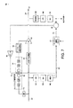
図3は、電力増幅器伝達関数が調節される例示的な配列を示し、図5は、送信機伝達関数が調節される例示的な配列を示す。このコンテキストでは、「送信機」という用語は、送信機RF変調器ブロック20と電力増幅器18との組み合わせを意味する。
FIG. 3 shows an exemplary arrangement in which the power amplifier transfer function is adjusted, and FIG. 5 shows an exemplary arrangement in which the transmitter transfer function is adjusted. In this context, the term “transmitter” refers to the combination of transmitter
任意の図における素子が、前の図に示された素子に対応する場合、同様の参照番号が使用される。 Where elements in any figure correspond to elements shown in previous figures, similar reference numerals are used.
図3は、第1の例示的な配列に係る例示的な回路の実装を例示する。 FIG. 3 illustrates an exemplary circuit implementation according to a first exemplary arrangement.
図3の配列は、成形が実際の電力増幅器伝達関数とターゲット電力増幅器伝達関数との間の誤差測定に基づくように成形が行われるエンベロープ追跡経路を構成する。 The arrangement of FIG. 3 constitutes an envelope tracking path in which shaping is performed such that shaping is based on an error measurement between the actual power amplifier transfer function and the target power amplifier transfer function.
図では、成形は誤差による差分に基づいており、本明細書では差分が説明されるが、実際には、成形は、信号間の任意の比較に基づき得る。これは、例えば、誤差というよりもむしろ相関又は比のような測定であり得る。 In the figure, shaping is based on differences due to errors, and differences are described herein, but in practice shaping can be based on any comparison between signals. This can be, for example, a measure such as a correlation or ratio rather than an error.
図3のエンベロープ追跡アーキテクチャは、図1のものに対応するが、復調器ブロック60及び66、AMブロック62及び68、S/H(サンプル及び保持)ブロック64及び70、ターゲット振幅ブロック72、誤差測定又は比較ブロック74、及びスケーリングブロック76が追加されている。
The envelope tracking architecture of FIG. 3 corresponds to that of FIG. 1, but demodulator blocks 60 and 66, AM blocks 62 and 68, S / H (sample and hold) blocks 64 and 70,
ライン24上のRF出力信号は、復調器66によって検出され、復調器66、AMブロック68、及びS/Hブロック70は、ライン24上のRF出力信号のエンベロープのデジタル表現であるライン71上の信号を供給するように動作する。電力増幅器の出力を表すライン71上のそのような信号の生成は、特定の実装に依存しない。
The RF output signal on
同様に、復調器ブロック60は、電力増幅器18への入力においてRF入力信号を受け、復調器ブロック60、AMブロック62、及びS/Hブロック64は、電力増幅器18へのRF入力信号のエンベロープのデジタル表現であるライン63上の信号を生成する。電力増幅器の入力を表すライン63上のそのような信号の生成は、特定の実装に依存しない。
Similarly, demodulator block 60 receives an RF input signal at the input to
ライン63上の電力増幅器の入力エンベロープ信号の測定はまた、ターゲット振幅ブロック72への入力として供給される。
A measurement of the power amplifier input envelope signal on
ターゲット振幅ブロックは、ターゲットAM−AM特性を記憶するように構成される。ターゲット振幅ブロック72は、このターゲットAM−AM特性によって調整された電力増幅器への実際の入力エンベロープであるライン73上の電力増幅器AM出力を生成する。このように、ターゲット振幅ブロック72は、ライン63上の信号の関数であるライン73上の信号を供給し、これは、電力増幅器18に適用されるRF入力信号のエンベロープである。
The target amplitude block is configured to store a target AM-AM characteristic. The
ターゲット振幅ブロック72のこのAM−AM特性は、増幅段の理想のAM−AM特性であり、増幅段のターゲットAM−AM特性を満たすために、電力増幅器18によって適用されることが望まれるAM−AM特性をライン63上の入力信号の表現に適用するために供給される。
This AM-AM characteristic of the
増幅段のAM−AM特性は、エンベロープ経路における成形テーブル30が増幅器18への供給信号を成形し、それによって、増幅器18が、所望のAM−AM特性を満たす増幅出力信号を供給することによって達成される。エンベロープ経路における成形テーブルは、ターゲットAM−AM特性が満たされるまで成形を適用する。
The AM-AM characteristic of the amplification stage is achieved by the shaping table 30 in the envelope path shaping the supply signal to the
ターゲット振幅ブロック72は、ライン63上の測定された入力信号に、理想又は所望のAM−AM特性を適用し、そして、ライン73上の入力信号の表現は、それに応じて、理想のAM−AM特性へと成形される。これは、出力信号との入力信号の後続の比較が、増幅器18のAM−AM特性を制御する際にエンベロープ経路の成形制御を考慮に入れることを意味する。
The
AM−AM特性は、線形ゲイン特性と同じくらいシンプルであり得るか、又は、効率性、線形性、又は広帯域ノイズのような、システムレベルパラメータを制御し得る、より精密なものであり得る。例えば、ピークレベルの低減、及びその調節が適用され得、これにより、電力増幅器のサイズの低減が可能になり、効率利益を提供するか、又は、成形テーブルのより低いエンドが調整され得、それは、例えば、温度シフトによる電力増幅器(PA)特性の変更にわたって広帯域ノイズレベルを制御することができる。 The AM-AM characteristic can be as simple as the linear gain characteristic, or it can be more precise that can control system level parameters such as efficiency, linearity, or broadband noise. For example, peak level reduction, and adjustments thereof, can be applied, which allows a reduction in the size of the power amplifier and provides an efficiency benefit, or the lower end of the molding table can be adjusted, For example, wideband noise levels can be controlled over power amplifier (PA) characteristic changes due to temperature shifts.
ライン11上の制御信号は、ターゲットAM−AM特性を設定するためにターゲット振幅ブロック72に制御を供給する。ライン11上の制御信号は、システムパラメータ又は対象(objective)であり得、ターゲット振幅ブロック72は、ターゲットAM−AM特性を決定するために、これらのパラメータを、例えば、ルックアップテーブル(LUT)に、又は、アルゴリズムを用いて、適用し得る。代替的に、ライン11上の制御信号は、ターゲットAM−AM特性であり得る。
A control signal on
誤差測定又は比較ブロック74は、2つの入力信号を受ける。1つは、ライン73上でターゲット振幅ブロック72によって理想又はターゲットAM−AM特性が適用されている電力増幅器への入力の実際のエンベロープであり、もう1つは、ライン71上の出力電力増幅器の実際のエンベロープである。
Error measurement or comparison block 74 receives two input signals. One is the actual envelope of the input to the power amplifier where the ideal or target AM-AM characteristic is applied by the
誤差測定又は比較ブロック74は、これら2つのエンベロープ信号を比較し、ライン75上の誤差測定ブロックの出力は、スケールブロック76の入力に供給される。ライン75上の誤差測定又は比較ブロック74の出力は、この実施形態では、その入力における2つの信号間の誤差である。
Error measurement or comparison block 74 compares these two envelope signals and the output of the error measurement block on
スケールブロック76は、好ましくは、それに適用されている信号をスケーリングし、ライン77上で制御入力を成形ブロックに伝達する増幅器又は減衰器である。
The
このように、成形ブロック30は、追加的に、実際の出力信号と、増幅器の理想ターゲットAM−AM特性よって調整された実際の入力信号との比較に依存して生成されるライン77上の信号を受け、ライン77上の信号は誤差を表す。
Thus, shaping
ライン63上の信号はまた、成形ブロック30の書込インデックスポートに直接的に供給され、成形ブロック30に、更新されるべきアドレス又はインデックスについて知らせる。ライン77上の信号は、更新において適用されるべき誤差値であり、ライン63上の信号は、更新されるべき成形ブロック30のアドレス又はインデックスである。
The signal on
この例では、成形関数へのインデックスは、比較でも使用される入力信号によって提供される。しかしながら、いくつかの実施形態では、同じ入力信号が使用されない可能性がある。インデックスは一般に、比較において使用される入力信号を表す信号によって提供される。出力信号は、例えば、入力信号の表現であり、入力信号の表現は、他のポイントで及び他の信号によって提供され得る。 In this example, the index to the shaping function is provided by the input signal that is also used in the comparison. However, in some embodiments, the same input signal may not be used. The index is generally provided by a signal that represents the input signal used in the comparison. The output signal is, for example, a representation of the input signal, which can be provided at other points and by other signals.
成形テーブルは、特定の入力(インデックス)のための関数を記憶し、この入力(インデックス)は、決定された誤差に基づいて更新又は修正される。 The shaping table stores a function for a particular input (index), which is updated or modified based on the determined error.
成形ブロック30は、説明された配列に従って4つのポートを有する。2つのポートは、成形ブロックの入力及び出力である。成形ブロック30は、入力を受け、成形関数をこの入力に適用し、次いで、成形関数が適用された入力(成形された入力)である出力を生成する。
The
第3のポートは、ライン63上の信号に接続されており、現在の入力に対して特定の成形関数を選択するために成形テーブルをインデックスし得る。好ましい配列では、1つの成形関数を有する1つの成形テーブルが存在し、これは、ポイント単位で構成される。即ち、ライン3は、更新されるべき成形テーブル内のポイント(又はインデックス)を選択し、その特定のポイントに対する新しい値が、ライン77上の補正値によって与えられる。
The third port is connected to the signal on
第4のポートは、選択された成形関数に行われるべき補正を表す、ライン77上の誤差信号である。
The fourth port is an error signal on
このように、成形ブロック30は、それが、この比較から決定された誤差に基づいて、及び、検出された実際の入力信号に基づいて成形関数をエンベロープ信号に適用するように構成される。
Thus, the shaping
図3の回路の動作は、図4のフロープロセスにおいて要約される。 The operation of the circuit of FIG. 3 is summarized in the flow process of FIG.
ステップ402によって表されるように、増幅されるべき入力信号を受け、ステップ404によって表されるように、入力信号がRFに変調される。ステップ406において、エンベロープ信号が、エンベロープ追跡変調器のために生成される。ステップ408において、エンベロープ追跡電源電圧が生成される。次いで、ステップ410において、エンベロープ追跡電源電圧が電力増幅器に供給される。次いで、ステップ412において、受けた入力信号が、電力増幅器へのエンベロープ追跡電源電圧に依存して増幅され、ステップ414において、出力信号が、電力増幅器の出力において生成される。
As represented by
ステップ416において、電力増幅器の実際の出力信号と、振幅ターゲット調整された入力信号との間で比較が行われる。ステップ418において、エンベロープ信号の生成が、この比較に依存して制御される。ステップ420において、エンベロープ信号の生成はまた、更新すべき成形関数を決定する現在の入力信号に依存して制御される。
In
成形ブロックは、ライン77上で誤差補正信号を受け、追加的にライン63上で入力信号の表現を受ける。このように、成形関数は、誤差補正が適用されることとなる特定の入力信号インデックスについて知っている。
The shaping block receives an error correction signal on
誤差信号は、AM入力レベルの関数であり、これは、2つの潜在的な利点を有する。 The error signal is a function of the AM input level, which has two potential advantages.
第1に、リアルタイムに成形テーブルを更新する必要はない。これは、要件の更新測定及び更新帯域幅を大幅に低くする。 First, there is no need to update the molding table in real time. This significantly reduces the requirement update measurement and update bandwidth.
実用的な実装では、更新の速度は、オプションのサンプル及び保持ブロックによって決定される。 In practical implementations, the update rate is determined by an optional sample and holding block.
例として、成形関数は、温度の変化の追跡を提供するために、極めてゆっくり追跡され得る。 As an example, the shaping function can be tracked very slowly to provide tracking of temperature changes.
第2に、更新を適用するときに正しいエンベロープ追跡経路成形テーブルインデックスをインデックスすること又は指すことは容易である。ライン63上の入力信号の表現は、このインデックスを提供する。
Second, it is easy to index or point to the correct envelope tracking path shaping table index when applying updates. The representation of the input signal on
所望の電力増幅器伝達関数を取得するためのこの差分に基づいたエンベロープ追跡経路成形関数の閉ループ補正は有益である。 A closed loop correction of the envelope tracking path shaping function based on this difference to obtain the desired power amplifier transfer function is beneficial.
一般に、誤差信号は、出力信号と、成形された入力信号とを比較することに基づき、信号の振幅(エンベロープ信号によって表されるような)又は信号の電力のような、これらの信号の任意の特性が比較され得る。 In general, the error signal is based on comparing the output signal with the shaped input signal, and any of these signals, such as signal amplitude (as represented by the envelope signal) or signal power. Properties can be compared.
図3の例示的な配列は、例示的な配列を提供するために、更に修正され得る。上述しように、図3は、出力信号の複製を入力信号の表現と比較することによって、振幅制御信号が生成される配列を開示し、ここで、入力信号の表現は、ターゲットAM−AM特性に従って調整される。この更なる例示的な配列では、位相制御信号が、出力信号の表現を入力信号の表現と比較することによって生成され、ここで、入力信号の表現は、ターゲットPM−PM特性に従って調整される。 The example arrangement of FIG. 3 can be further modified to provide an example arrangement. As described above, FIG. 3 discloses an arrangement in which an amplitude control signal is generated by comparing a replica of the output signal with a representation of the input signal, where the representation of the input signal is in accordance with the target AM-AM characteristic. Adjusted. In this further exemplary arrangement, the phase control signal is generated by comparing the representation of the output signal with the representation of the input signal, where the representation of the input signal is adjusted according to the target PM-PM characteristic.
説明された例示的な配列では、位相制御信号の生成は、振幅制御信号の生成と組み合わせられて示される。実際、一方又は両方の制御信号が生成される。 In the exemplary arrangement described, the generation of the phase control signal is shown in combination with the generation of the amplitude control signal. In fact, one or both control signals are generated.
図5は、更なる修正がおこなわれた図3の配列を例示する。図3のものに対応する図5の素子は、それらが、図3の説明された素子に対応するため、再度説明されない。 FIG. 5 illustrates the arrangement of FIG. 3 with further modifications. The elements of FIG. 5 that correspond to those of FIG. 3 will not be described again because they correspond to the described elements of FIG.
図5では、図3の配列が、比較ブロック74'及びターゲット位相ブロック72'を含めることによって更に修正される。図3のAMブロックは、AM/PMブロック62'になるように修正され、図3のAMブロック68は、AM/PMブロック68'になるように修正される。
In FIG. 5, the arrangement of FIG. 3 is further modified by including a comparison block 74 ′ and a
ターゲット位相ブロック72'は、ライン11'上で制御信号を受け、これは、好ましくは、増幅段のためのターゲットPM−PM特性である。このように、ターゲット位相ブロック72'は、ライン63上の入力信号にターゲットPM−PM特性を適用し、比較ブロック74'は、これを、ライン71上の出力信号の表現と比較する。ターゲット位相ブロック72'は、ライン63上の信号内のPM情報だけを調べ(look at)、ターゲット振幅ブロック72は、ライン63上の信号内のAM情報だけを調べる。
The target phase block 72 'receives a control signal on line 11', which is preferably the target PM-PM characteristic for the amplification stage. Thus,
比較ブロック74'の出力は、比較に依存して増幅器への入力信号の位相を調整するために、送信機RF変調器ブロック20へ入力として供給される。
The output of the comparison block 74 'is provided as an input to the transmitter
AMブロック62及び68のAM/PMブロック62'及び68'への調整は、それぞれの信号の位相が含まれること及び比較器74'で比較されることを可能にする。 Adjustment of AM blocks 62 and 68 to AM / PM blocks 62 'and 68' allows the phases of the respective signals to be included and compared in comparator 74 '.
図5は、信号ライン30から成形ブロック30への入力ポートにおいてAMブロック21をもたらすことによって図3の配列を更に修正する。ET経路における成形ブロック30の「書込インデックスポート」は、AMインデックス信号を受け、このAMブロック21は、成形ブロック30への適用のために、ライン63信号のAMコンテンツだけを導出する。
FIG. 5 further modifies the arrangement of FIG. 3 by providing an
図5の回路の動作は、図6のフロープロセスで概説される。図6は、図4に対応し、ステップ421及び423が追加されている。ステップ421において、電力増幅器の、実際の出力信号と、ターゲット位相調整された入力信号との間で比較が行われる。ステップ423において、電力増幅器への入力信号は、その比較に依存して調整される。
The operation of the circuit of FIG. 5 is outlined in the flow process of FIG. FIG. 6 corresponds to FIG. 4 and
図3は、振幅制御信号が生成される第1の例示的な配列を例示し、図5は、追加的に位相制御信号が生成される第2の例示的な配列を例示する。上述したように、振幅及び位相制御信号が両方とも生成され得るか、又はいくつかの実装では、これらの信号のうち1つだけが生成され得る。 FIG. 3 illustrates a first exemplary arrangement in which an amplitude control signal is generated, and FIG. 5 illustrates a second exemplary arrangement in which a phase control signal is additionally generated. As noted above, both amplitude and phase control signals can be generated, or in some implementations only one of these signals can be generated.
図7は、図3の第1の例示的な配列に基づいて、第3の例示的な配列に係る例示的な回路の配列を例示する。 FIG. 7 illustrates an exemplary circuit arrangement according to the third exemplary arrangement based on the first exemplary arrangement of FIG.
図7のこの代替的な配列では、図3にあるような電力増幅器伝達関数というよりもむしろ送信機伝達関数が訂正される。上述したように、このコンテキストでは、「送信機」は、送信機RF変調器ブロックと電力増幅器との組み合わせを意味する。 In this alternative arrangement of FIG. 7, the transmitter transfer function is corrected rather than the power amplifier transfer function as in FIG. As mentioned above, in this context, “transmitter” means a combination of a transmitter RF modulator block and a power amplifier.
図7の例示的な配列から見受けられ得るように、図3のものに類似した回路が提供される。しかしながら、入力は、電力増幅器18への入力というよりはむしろ送信RF変調器ブロック20への入力から得られる。このように、図3の復調器60は必要とされない。AMブロック62は、ライン22上で直接的に入力を受け、これを、サンプル及び保持ブロック64に供給する。AMブロック12の出力が図7のAMブロック62の代わりに使用もされ得ることに留意されたい。サンプル及び保持ブロック64の出力が、遅延ブロック80に適用される。遅延ブロック80は、送信RF変調器ブロック20による遅延を補償するため、及び、誤差測定又は比較ブロック74の2つの入力信号のタイミングをアラインするために提供される。遅延ブロック80の出力は、ライン63上で、成形テーブル30の書込インデックスポートへの入力として、また、図3の配列と合せて、ターゲットAM−AM特性を記憶するターゲット振幅ブロック72への入力として供給される。
As can be seen from the exemplary arrangement of FIG. 7, a circuit similar to that of FIG. 3 is provided. However, the input is derived from the input to transmit
図7の配列は、そうでなければ図3の配列と合され、単に、電力増幅器単独の性能というよりはむしろ送信機全体の性能が修正される配列を例示するにすぎない。この修正方法を選定することで、RFダウンコンバージョン又はアナログ/デジタル変換プロセスは何れも電力増幅器の入力側で必要とされない。 The arrangement of FIG. 7 is otherwise combined with the arrangement of FIG. 3 and merely illustrates an arrangement in which the performance of the entire transmitter is modified rather than the performance of the power amplifier alone. By selecting this modification method, no RF downconversion or analog / digital conversion process is required on the input side of the power amplifier.
図7の配列の動作は、図8のプロセスにおいて示される。ステップ610において、増幅されるべきRF入力信号を受け、ステップ612において、この受けた入力信号がRFに変調される。ステップ614において、エンベロープ信号が、エンベロープ追跡変調器のために生成され、次いで、ステップ616において、追跡電源電圧が、このエンベロープ信号に依存して生成される。ステップ618において、エンベロープ追跡電源電圧が電力増幅器に供給される。次いで、ステップ620において、受けた入力信号が、電力増幅器へのエンベロープ追跡電源電圧に依存して増幅される。ステップ622において、RF出力信号が電力増幅器の出力において生成される。
The operation of the arrangement of FIG. 7 is illustrated in the process of FIG. In
ステップ624において、増幅器の実際の出力信号と、振幅ターゲット調整された入力信号との間で、入力信号に基づいて比較が行われる。ステップ626において、エンベロープ信号の生成が、この比較に依存して制御され、ステップ628で例示されているように、このエンベロープ信号の制御はまた、入力信号に依存して達成される。
In
図3及び図7の配列から理解されるであろうように、電力増幅器又は送信機伝達関数を調節することが望まれようと望まれないと、好ましくは同様のアプローチが取られる。図5の技法に係る、位相制御信号の生成は何れも図7には示されていないが、図7の例示的な配列が、図5に示されるような位相制御信号を生成するように構成され得ることは明らかであろう。 As will be appreciated from the arrangement of FIGS. 3 and 7, a similar approach is preferably taken if it is desired or not desired to adjust the power amplifier or transmitter transfer function. Although none of the phase control signal generation according to the technique of FIG. 5 is shown in FIG. 7, the exemplary arrangement of FIG. 7 is configured to generate a phase control signal as shown in FIG. It will be clear that it can be done.
説明された配列の目的は、温度又は時間にわたる電力増幅器特性のシフトによる電力増幅器の線形性を調節することであり得る。追加的に、エンベロープ追跡経路のスイング範囲を制限しつつ線形性のレベルを維持するものに伝達関数を調節することが望まれるだろう。 The purpose of the described arrangement can be to adjust the linearity of the power amplifier by shifting the power amplifier characteristics over temperature or time. Additionally, it may be desirable to adjust the transfer function to maintain the level of linearity while limiting the swing range of the envelope tracking path.
説明された配列の可能な(possible)用途の別の例は、例えば、電力レベルにわたって電力増幅器出力信号の一定のピーク対アベレージを維持するために、ターゲット出力電力レベルに対する電力増幅器特性を更新することである。 Another example of a possible use of the described arrangement is to update the power amplifier characteristics relative to the target output power level, eg, to maintain a constant peak-to-average of the power amplifier output signal across the power level It is.
本明細書で提案されたシステムには多くの用途が存在する可能性があり、ターゲット伝達関数は、本明細書では特定されない。ターゲット伝達関数は、最終生成物の性能要件に依存して設定され得る一般の「ターゲット成形」ブロックとして説明されている。当業者は、ターゲット伝達関数を設定するための実装例を理解するだろう。 There can be many uses for the proposed system, and the target transfer function is not specified here. The target transfer function is described as a general “target shaping” block that can be set depending on the performance requirements of the final product. Those skilled in the art will understand implementation examples for setting the target transfer function.
本発明は、本明細書において、特定の利点のある実施形態及び例示的な実装を参照して説明されている。本発明は、そのような実施形態及び実装の任意の態様の任意の詳細に限定されるわけではない。本発明の範囲は、添付の特許請求の範囲によって定義される。 The present invention has been described herein with reference to certain advantageous embodiments and exemplary implementations. The invention is not limited to any details of any aspects of such embodiments and implementations. The scope of the present invention is defined by the appended claims.
Claims (17)
前記増幅器の前記出力信号の表現を決定することと、
前記増幅器の前記入力信号の表現を決定することと、
前記増幅器のターゲット特性に従って前記入力信号の前記決定された表現を調整することと、
前記調整された入力と、前記出力の決定された表現とを比較することと、
前記比較に依存して制御信号を生成することと
を備える方法。 A method for controlling in an envelope tracking amplification stage, comprising:
Determining a representation of the output signal of the amplifier;
Determining a representation of the input signal of the amplifier;
Adjusting the determined representation of the input signal according to a target characteristic of the amplifier;
Comparing the adjusted input with a determined representation of the output;
Generating a control signal in dependence upon the comparison.
Applications Claiming Priority (3)
| Application Number | Priority Date | Filing Date | Title |
|---|---|---|---|
| GBGB1309235.8A GB201309235D0 (en) | 2013-05-22 | 2013-05-22 | Transfer function regulation |
| GB1309235.8 | 2013-05-22 | ||
| PCT/EP2014/060583 WO2014187920A1 (en) | 2013-05-22 | 2014-05-22 | Transfer function regulation |
Publications (2)
| Publication Number | Publication Date |
|---|---|
| JP2016518800A true JP2016518800A (en) | 2016-06-23 |
| JP2016518800A5 JP2016518800A5 (en) | 2017-06-15 |
Family
ID=48747170
Family Applications (1)
| Application Number | Title | Priority Date | Filing Date |
|---|---|---|---|
| JP2016514420A Pending JP2016518800A (en) | 2013-05-22 | 2014-05-22 | Transfer function adjustment |
Country Status (9)
| Country | Link |
|---|---|
| US (1) | US9793858B2 (en) |
| EP (1) | EP3000174A1 (en) |
| JP (1) | JP2016518800A (en) |
| KR (1) | KR20160013078A (en) |
| CN (1) | CN105229919B (en) |
| BR (1) | BR112015029178A2 (en) |
| GB (1) | GB201309235D0 (en) |
| MX (1) | MX350424B (en) |
| WO (1) | WO2014187920A1 (en) |
Families Citing this family (29)
| Publication number | Priority date | Publication date | Assignee | Title |
|---|---|---|---|---|
| US10158330B1 (en) | 2017-07-17 | 2018-12-18 | Qorvo Us, Inc. | Multi-mode envelope tracking amplifier circuit |
| US10944365B2 (en) | 2018-06-28 | 2021-03-09 | Qorvo Us, Inc. | Envelope tracking amplifier circuit |
| US11088618B2 (en) | 2018-09-05 | 2021-08-10 | Qorvo Us, Inc. | PWM DC-DC converter with linear voltage regulator for DC assist |
| US10911001B2 (en) | 2018-10-02 | 2021-02-02 | Qorvo Us, Inc. | Envelope tracking amplifier circuit |
| US11018638B2 (en) | 2018-10-31 | 2021-05-25 | Qorvo Us, Inc. | Multimode envelope tracking circuit and related apparatus |
| US10985702B2 (en) | 2018-10-31 | 2021-04-20 | Qorvo Us, Inc. | Envelope tracking system |
| US10938351B2 (en) | 2018-10-31 | 2021-03-02 | Qorvo Us, Inc. | Envelope tracking system |
| US11031909B2 (en) | 2018-12-04 | 2021-06-08 | Qorvo Us, Inc. | Group delay optimization circuit and related apparatus |
| US11082007B2 (en) | 2018-12-19 | 2021-08-03 | Qorvo Us, Inc. | Envelope tracking integrated circuit and related apparatus |
| US11146213B2 (en) | 2019-01-15 | 2021-10-12 | Qorvo Us, Inc. | Multi-radio access technology envelope tracking amplifier apparatus |
| US11025458B2 (en) * | 2019-02-07 | 2021-06-01 | Qorvo Us, Inc. | Adaptive frequency equalizer for wide modulation bandwidth envelope tracking |
| US10998859B2 (en) | 2019-02-07 | 2021-05-04 | Qorvo Us, Inc. | Dual-input envelope tracking integrated circuit and related apparatus |
| US11233481B2 (en) | 2019-02-18 | 2022-01-25 | Qorvo Us, Inc. | Modulated power apparatus |
| US11374482B2 (en) | 2019-04-02 | 2022-06-28 | Qorvo Us, Inc. | Dual-modulation power management circuit |
| US11082009B2 (en) | 2019-04-12 | 2021-08-03 | Qorvo Us, Inc. | Envelope tracking power amplifier apparatus |
| US11018627B2 (en) | 2019-04-17 | 2021-05-25 | Qorvo Us, Inc. | Multi-bandwidth envelope tracking integrated circuit and related apparatus |
| US11424719B2 (en) | 2019-04-18 | 2022-08-23 | Qorvo Us, Inc. | Multi-bandwidth envelope tracking integrated circuit |
| US11031911B2 (en) | 2019-05-02 | 2021-06-08 | Qorvo Us, Inc. | Envelope tracking integrated circuit and related apparatus |
| US11349436B2 (en) | 2019-05-30 | 2022-05-31 | Qorvo Us, Inc. | Envelope tracking integrated circuit |
| US11539289B2 (en) | 2019-08-02 | 2022-12-27 | Qorvo Us, Inc. | Multi-level charge pump circuit |
| US11309922B2 (en) | 2019-12-13 | 2022-04-19 | Qorvo Us, Inc. | Multi-mode power management integrated circuit in a small formfactor wireless apparatus |
| US11349513B2 (en) | 2019-12-20 | 2022-05-31 | Qorvo Us, Inc. | Envelope tracking system |
| US11539330B2 (en) | 2020-01-17 | 2022-12-27 | Qorvo Us, Inc. | Envelope tracking integrated circuit supporting multiple types of power amplifiers |
| US11716057B2 (en) | 2020-01-28 | 2023-08-01 | Qorvo Us, Inc. | Envelope tracking circuitry |
| US11728774B2 (en) | 2020-02-26 | 2023-08-15 | Qorvo Us, Inc. | Average power tracking power management integrated circuit |
| US11196392B2 (en) | 2020-03-30 | 2021-12-07 | Qorvo Us, Inc. | Device and device protection system |
| US11588449B2 (en) | 2020-09-25 | 2023-02-21 | Qorvo Us, Inc. | Envelope tracking power amplifier apparatus |
| US11728796B2 (en) | 2020-10-14 | 2023-08-15 | Qorvo Us, Inc. | Inverted group delay circuit |
| US11909385B2 (en) | 2020-10-19 | 2024-02-20 | Qorvo Us, Inc. | Fast-switching power management circuit and related apparatus |
Citations (3)
| Publication number | Priority date | Publication date | Assignee | Title |
|---|---|---|---|---|
| JP2010541326A (en) * | 2007-09-20 | 2010-12-24 | クアンタンス, インコーポレイテッド | Power amplifier controller having a polar transmitter |
| JP2011228999A (en) * | 2010-04-21 | 2011-11-10 | Sumitomo Electric Ind Ltd | Amplifier circuit and wireless communication device |
| WO2012086830A1 (en) * | 2010-12-20 | 2012-06-28 | 日本電気株式会社 | Amplifier device and method of controlling same |
Family Cites Families (10)
| Publication number | Priority date | Publication date | Assignee | Title |
|---|---|---|---|---|
| JPH07118617B2 (en) * | 1990-07-19 | 1995-12-18 | 沖電気工業株式会社 | Power amplifier and transmitter |
| GB2370435A (en) | 2000-12-22 | 2002-06-26 | Nokia Mobile Phones Ltd | A polar loop transmitter for a mobile phone |
| US7805115B1 (en) * | 2003-06-02 | 2010-09-28 | Analog Devices, Inc. | Variable filter systems and methods for enhanced data rate communication systems |
| US7706467B2 (en) | 2004-12-17 | 2010-04-27 | Andrew Llc | Transmitter with an envelope tracking power amplifier utilizing digital predistortion of the signal envelope |
| US7518445B2 (en) * | 2006-06-04 | 2009-04-14 | Samsung Electro-Mechanics Company, Ltd. | Systems, methods, and apparatuses for linear envelope elimination and restoration transmitters |
| CN101090381A (en) * | 2006-06-04 | 2007-12-19 | 三星电机株式会社 | Systems, methods, and apparatuses for multi-path orthogonal predistorters |
| CN101247153B (en) | 2008-03-13 | 2011-11-30 | 中兴通讯股份有限公司 | Method for improving power amplifier efficiency and digital predistortion broadband communicator |
| EP2673881B1 (en) * | 2011-02-07 | 2019-02-06 | Skyworks Solutions, Inc. | Apparatus and methods for envelope tracking calibration |
| GB2489040B (en) * | 2011-03-17 | 2018-04-04 | Snaptrack Inc | Timing alignment for power amplifier |
| CN102723915B (en) | 2012-07-06 | 2016-02-24 | 厦门大学 | A kind of applicable hard-wired question blank digital pre-distortion method and device |
-
2013
- 2013-05-22 GB GBGB1309235.8A patent/GB201309235D0/en not_active Ceased
-
2014
- 2014-05-22 KR KR1020157035640A patent/KR20160013078A/en not_active Application Discontinuation
- 2014-05-22 BR BR112015029178A patent/BR112015029178A2/en not_active Application Discontinuation
- 2014-05-22 US US14/892,517 patent/US9793858B2/en active Active
- 2014-05-22 JP JP2016514420A patent/JP2016518800A/en active Pending
- 2014-05-22 WO PCT/EP2014/060583 patent/WO2014187920A1/en active Application Filing
- 2014-05-22 MX MX2015016027A patent/MX350424B/en active IP Right Grant
- 2014-05-22 CN CN201480028789.XA patent/CN105229919B/en active Active
- 2014-05-22 EP EP14730445.5A patent/EP3000174A1/en not_active Ceased
Patent Citations (3)
| Publication number | Priority date | Publication date | Assignee | Title |
|---|---|---|---|---|
| JP2010541326A (en) * | 2007-09-20 | 2010-12-24 | クアンタンス, インコーポレイテッド | Power amplifier controller having a polar transmitter |
| JP2011228999A (en) * | 2010-04-21 | 2011-11-10 | Sumitomo Electric Ind Ltd | Amplifier circuit and wireless communication device |
| WO2012086830A1 (en) * | 2010-12-20 | 2012-06-28 | 日本電気株式会社 | Amplifier device and method of controlling same |
Also Published As
| Publication number | Publication date |
|---|---|
| KR20160013078A (en) | 2016-02-03 |
| GB201309235D0 (en) | 2013-07-03 |
| US9793858B2 (en) | 2017-10-17 |
| EP3000174A1 (en) | 2016-03-30 |
| MX2015016027A (en) | 2016-03-21 |
| BR112015029178A2 (en) | 2017-07-25 |
| MX350424B (en) | 2017-09-05 |
| CN105229919A (en) | 2016-01-06 |
| WO2014187920A1 (en) | 2014-11-27 |
| US20160126900A1 (en) | 2016-05-05 |
| CN105229919B (en) | 2020-10-13 |
Similar Documents
| Publication | Publication Date | Title |
|---|---|---|
| US9793858B2 (en) | Transfer function regulation | |
| US9998241B2 (en) | Envelope tracking (ET) closed-loop on-the-fly calibration | |
| JP6166457B2 (en) | Envelope tracking system with internal power amplifier characterization | |
| JP6138158B2 (en) | Distortion compensation in RF path combined with shaping table in envelope path for envelope tracking amplifier | |
| US8928403B2 (en) | Envelope path processing for envelope tracking amplification stage | |
| US7535298B2 (en) | Arrangement and a method relating to signal predistortion | |
| US8391808B2 (en) | Method and system for estimating and compensating non-linear distortion in a transmitter using calibration | |
| US6968163B2 (en) | Method and transmission circuit for generating a transmission signal | |
| US20100189193A1 (en) | Polar modulation transmitter and polar modulation transmission method | |
| JP2016519545A (en) | Delay adjustment | |
| JP2002100940A (en) | Distortion compensation amplifier | |
| TW200838125A (en) | Amplifying circuit and wireless communication device | |
| JP4009640B2 (en) | Method and apparatus for adjusting transmit power in a multi-rate wireless communication system | |
| JP2005269440A (en) | Polar modulation transmitter and polar modulation method | |
| US8699976B2 (en) | Transmitter with hybrid closed loop power control | |
| WO2012059068A1 (en) | Method, device and communication system for correcting polar transmitter delay skew | |
| US7940859B2 (en) | Transmission circuit and communication device | |
| WO2003039010A1 (en) | Transmission apparatus and automatic gain control method thereof | |
| US20160182099A1 (en) | Systems and methods for efficient multi-channel satcom with dynamic power supply and digital pre-distortion | |
| JP2005150814A (en) | Method and apparatus of compensating non-linear distortion | |
| US20150072631A1 (en) | Amplifier and amplification method | |
| CN103428133A (en) | Predistortion temperature compensation device and method, predistorter and transmitter |
Legal Events
| Date | Code | Title | Description |
|---|---|---|---|
| A521 | Request for written amendment filed |
Free format text: JAPANESE INTERMEDIATE CODE: A523 Effective date: 20170426 |
|
| A621 | Written request for application examination |
Free format text: JAPANESE INTERMEDIATE CODE: A621 Effective date: 20170426 |
|
| A977 | Report on retrieval |
Free format text: JAPANESE INTERMEDIATE CODE: A971007 Effective date: 20180531 |
|
| A131 | Notification of reasons for refusal |
Free format text: JAPANESE INTERMEDIATE CODE: A131 Effective date: 20180626 |
|
| A601 | Written request for extension of time |
Free format text: JAPANESE INTERMEDIATE CODE: A601 Effective date: 20180921 |
|
| A521 | Request for written amendment filed |
Free format text: JAPANESE INTERMEDIATE CODE: A523 Effective date: 20181126 |
|
| A131 | Notification of reasons for refusal |
Free format text: JAPANESE INTERMEDIATE CODE: A131 Effective date: 20190416 |
|
| A02 | Decision of refusal |
Free format text: JAPANESE INTERMEDIATE CODE: A02 Effective date: 20191112 |