JP2016519545A - Delay adjustment - Google Patents
Delay adjustment Download PDFInfo
- Publication number
- JP2016519545A JP2016519545A JP2016514418A JP2016514418A JP2016519545A JP 2016519545 A JP2016519545 A JP 2016519545A JP 2016514418 A JP2016514418 A JP 2016514418A JP 2016514418 A JP2016514418 A JP 2016514418A JP 2016519545 A JP2016519545 A JP 2016519545A
- Authority
- JP
- Japan
- Prior art keywords
- signal
- input
- envelope
- path
- slope
- Prior art date
- Legal status (The legal status is an assumption and is not a legal conclusion. Google has not performed a legal analysis and makes no representation as to the accuracy of the status listed.)
- Pending
Links
- 230000003321 amplification Effects 0.000 claims abstract description 23
- 238000003199 nucleic acid amplification method Methods 0.000 claims abstract description 23
- 230000001934 delay Effects 0.000 claims abstract description 14
- 238000000034 method Methods 0.000 claims description 16
- 230000003247 decreasing effect Effects 0.000 description 12
- 230000003111 delayed effect Effects 0.000 description 6
- 230000000630 rising effect Effects 0.000 description 6
- 238000013016 damping Methods 0.000 description 5
- 238000007493 shaping process Methods 0.000 description 3
- 238000005259 measurement Methods 0.000 description 2
- 230000001419 dependent effect Effects 0.000 description 1
- 230000010354 integration Effects 0.000 description 1
- 230000000717 retained effect Effects 0.000 description 1
- 230000003595 spectral effect Effects 0.000 description 1
- 230000001360 synchronised effect Effects 0.000 description 1
Images


Classifications
-
- H—ELECTRICITY
- H03—ELECTRONIC CIRCUITRY
- H03F—AMPLIFIERS
- H03F1/00—Details of amplifiers with only discharge tubes, only semiconductor devices or only unspecified devices as amplifying elements
- H03F1/02—Modifications of amplifiers to raise the efficiency, e.g. gliding Class A stages, use of an auxiliary oscillation
- H03F1/0205—Modifications of amplifiers to raise the efficiency, e.g. gliding Class A stages, use of an auxiliary oscillation in transistor amplifiers
- H03F1/0211—Modifications of amplifiers to raise the efficiency, e.g. gliding Class A stages, use of an auxiliary oscillation in transistor amplifiers with control of the supply voltage or current
- H03F1/0216—Continuous control
- H03F1/0222—Continuous control by using a signal derived from the input signal
-
- H—ELECTRICITY
- H03—ELECTRONIC CIRCUITRY
- H03F—AMPLIFIERS
- H03F3/00—Amplifiers with only discharge tubes or only semiconductor devices as amplifying elements
- H03F3/189—High-frequency amplifiers, e.g. radio frequency amplifiers
- H03F3/19—High-frequency amplifiers, e.g. radio frequency amplifiers with semiconductor devices only
-
- H—ELECTRICITY
- H03—ELECTRONIC CIRCUITRY
- H03F—AMPLIFIERS
- H03F3/00—Amplifiers with only discharge tubes or only semiconductor devices as amplifying elements
- H03F3/20—Power amplifiers, e.g. Class B amplifiers, Class C amplifiers
- H03F3/21—Power amplifiers, e.g. Class B amplifiers, Class C amplifiers with semiconductor devices only
-
- H—ELECTRICITY
- H03—ELECTRONIC CIRCUITRY
- H03F—AMPLIFIERS
- H03F1/00—Details of amplifiers with only discharge tubes, only semiconductor devices or only unspecified devices as amplifying elements
- H03F1/02—Modifications of amplifiers to raise the efficiency, e.g. gliding Class A stages, use of an auxiliary oscillation
- H03F1/0205—Modifications of amplifiers to raise the efficiency, e.g. gliding Class A stages, use of an auxiliary oscillation in transistor amplifiers
- H03F1/0211—Modifications of amplifiers to raise the efficiency, e.g. gliding Class A stages, use of an auxiliary oscillation in transistor amplifiers with control of the supply voltage or current
- H03F1/0216—Continuous control
- H03F1/0222—Continuous control by using a signal derived from the input signal
- H03F1/0227—Continuous control by using a signal derived from the input signal using supply converters
-
- H—ELECTRICITY
- H03—ELECTRONIC CIRCUITRY
- H03F—AMPLIFIERS
- H03F1/00—Details of amplifiers with only discharge tubes, only semiconductor devices or only unspecified devices as amplifying elements
- H03F1/02—Modifications of amplifiers to raise the efficiency, e.g. gliding Class A stages, use of an auxiliary oscillation
- H03F1/0205—Modifications of amplifiers to raise the efficiency, e.g. gliding Class A stages, use of an auxiliary oscillation in transistor amplifiers
- H03F1/0211—Modifications of amplifiers to raise the efficiency, e.g. gliding Class A stages, use of an auxiliary oscillation in transistor amplifiers with control of the supply voltage or current
- H03F1/0244—Stepped control
-
- H—ELECTRICITY
- H03—ELECTRONIC CIRCUITRY
- H03F—AMPLIFIERS
- H03F2200/00—Indexing scheme relating to amplifiers
- H03F2200/102—A non-specified detector of a signal envelope being used in an amplifying circuit
-
- H—ELECTRICITY
- H03—ELECTRONIC CIRCUITRY
- H03F—AMPLIFIERS
- H03F2200/00—Indexing scheme relating to amplifiers
- H03F2200/451—Indexing scheme relating to amplifiers the amplifier being a radio frequency amplifier
-
- H—ELECTRICITY
- H03—ELECTRONIC CIRCUITRY
- H03G—CONTROL OF AMPLIFICATION
- H03G3/00—Gain control in amplifiers or frequency changers
- H03G3/20—Automatic control
- H03G3/30—Automatic control in amplifiers having semiconductor devices
-
- H—ELECTRICITY
- H03—ELECTRONIC CIRCUITRY
- H03G—CONTROL OF AMPLIFICATION
- H03G3/00—Gain control in amplifiers or frequency changers
- H03G3/20—Automatic control
- H03G3/30—Automatic control in amplifiers having semiconductor devices
- H03G3/3005—Automatic control in amplifiers having semiconductor devices in amplifiers suitable for low-frequencies, e.g. audio amplifiers
- H03G3/301—Automatic control in amplifiers having semiconductor devices in amplifiers suitable for low-frequencies, e.g. audio amplifiers the gain being continuously variable
- H03G3/3015—Automatic control in amplifiers having semiconductor devices in amplifiers suitable for low-frequencies, e.g. audio amplifiers the gain being continuously variable using diodes or transistors
Landscapes
- Engineering & Computer Science (AREA)
- Power Engineering (AREA)
- Amplifiers (AREA)
Abstract
入力経路及びエンベロープ経路、並びに入力経路及びエンベロープ経路のうちの1つにある遅延段を備えるエンベロープ追跡増幅段が開示され、遅延段の遅延は、入力を表す信号のスロープ極性と、入力経路内の信号がエンベロープ経路内の信号に先行するか遅行するかに依存して決定される。【選択図】 図3An envelope tracking amplification stage comprising an input path and an envelope path and a delay stage in one of the input path and envelope path is disclosed, wherein the delay of the delay stage is determined by the slope polarity of the signal representing the input, It is determined depending on whether the signal precedes or delays the signal in the envelope path. [Selection] Figure 3
Description
本発明は、エンベロープ追跡増幅段における信号の制御に関する。 The present invention relates to signal control in an envelope tracking amplification stage.
エンベロープ追跡増幅段は当技術分野において周知であり、ここにおいて、電力増幅器への電源は、増幅されるべき入力信号のエンベロープに基づくように制御される。電力増幅器は、増幅されるべき入力信号を受け、加えて、増幅されるべき入力信号のエンベロープに依存して変調される電力供給を受ける。このように、増幅される出力信号は、効率的な方法で生成される。 Envelope tracking amplification stages are well known in the art, where the power supply to the power amplifier is controlled to be based on the envelope of the input signal to be amplified. The power amplifier receives an input signal to be amplified and in addition a power supply that is modulated depending on the envelope of the input signal to be amplified. In this way, the amplified output signal is generated in an efficient manner.
電力増幅器のための電力を生成するために変調器を制御するエンベロープ信号を成形するためにエンベロープ経路において処理を提供することは当技術分野で知られている。 It is known in the art to provide processing in the envelope path to shape the envelope signal that controls the modulator to generate power for the power amplifier.
電力増幅器に伝達される瞬間電力が入力信号の瞬間レベルに対応することを確実にするために、電力増幅器への入力経路、又は、電力増幅器への給電のためのエンベロープ経路の何れかにおいて遅延を提供することも先行技術で知られている。 In order to ensure that the instantaneous power delivered to the power amplifier corresponds to the instantaneous level of the input signal, a delay is provided either in the input path to the power amplifier or in the envelope path for feeding the power amplifier. Providing is also known in the prior art.
説明の目的上、エンベロープ経路と(RF)入力経路との間に固有の遅延差は存在しないものと想定される。 For purposes of explanation, it is assumed that there is no inherent delay difference between the envelope path and the (RF) input path.
RFエンベロープが正のスロープを有する場合、電源電圧の遅延は、電源電圧が所望のターゲットレベルを僅かに下回ることを意味し、その結果、出力が同様に僅かに低いため、RF出力エンベロープがそのターゲットに到達することを妨げる。同じ根拠で、RFエンベロープが負のスロープを有する場合、電源電圧の遅延は、RF出力エンベロープが若干高すぎることを意味する。 If the RF envelope has a positive slope, a power supply voltage delay means that the power supply voltage is slightly below the desired target level, so that the output is also slightly lower so that the RF output envelope is at its target. Prevent you from reaching. On the same basis, if the RF envelope has a negative slope, a delay in the supply voltage means that the RF output envelope is slightly too high.
遅延がRFエンベロープ信号に適用されると、RFエンベロープが正のスロープを有する場合、電源電圧の遅延は、それがターゲットを僅かに上回ることを意味し、その結果、RF出力エンベロープに、そのターゲットを上回らせる。同じ根拠で、RFエンベロープが負のスロープを有する場合、電源電圧の遅延は、RF出力エンベロープが若干低すぎることを意味する。 When a delay is applied to the RF envelope signal, if the RF envelope has a positive slope, the power supply voltage delay means that it is slightly above the target, so that the RF output envelope has its target Let me out. On the same basis, if the RF envelope has a negative slope, a delay in the supply voltage means that the RF output envelope is slightly too low.
効率を高めるためにエンベロープ追跡増幅段において適用される遅延を制御するための基礎を提供することが本発明の目的である。 It is an object of the present invention to provide a basis for controlling the delay applied in the envelope tracking amplification stage to increase efficiency.
一態様では、本発明は、入力経路及びエンベロープ経路、並びに入力経路及びエンベロープ経路のうちの1つにある遅延段を備えるエンベロープ追跡増幅段を提供し、遅延段の遅延は、入力を表す信号のスロープ極性と、入力経路内の信号がエンベロープ経路内の信号に先行するか遅行するかに依存して決定される。 In one aspect, the present invention provides an envelope tracking amplification stage comprising an input path and an envelope path, and a delay stage in one of the input path and envelope path, the delay of the delay stage being a signal representing the input. It is determined depending on the slope polarity and whether the signal in the input path precedes or delays the signal in the envelope path.
増幅されている現在の信号のスロープを識別する必要があるが、これは、多数の異なる信号、及び、好ましくは入力信号から直接導出された信号のスロープに基づいて決定され得る。このスロープは入力信号自体に基づいて決定され得るが、これはまた、例えば、増幅器の出力信号又はエンベロープ信号に基づいても決定され得る。 It is necessary to identify the slope of the current signal being amplified, but this can be determined based on a number of different signals and preferably the slope of the signal derived directly from the input signal. This slope can be determined based on the input signal itself, but it can also be determined based on, for example, an amplifier output signal or an envelope signal.
入力経路内の信号がエンベロープ経路内の信号に先行するか遅行するかは、多数の異なる信号、及び、好ましくは、入力経路及びエンベロープ経路内の信号から導出された又はそれを表す信号を比較することによって決定され得る。例えば、エンベロープ経路及び入力経路内の信号のタイミングを表す任意の信号が比較され得る。 Whether a signal in the input path precedes or delays a signal in the envelope path compares a number of different signals, and preferably a signal derived from or representing a signal in the input path and the envelope path Can be determined. For example, any signal representing the timing of signals in the envelope path and the input path can be compared.
入力を表す信号のスロープ極性は、入力経路、エンベロープ経路、又は出力経路内の信号のうちの何れか1つのスロープ極性を決定することによって決定され得る。 The slope polarity of the signal representing the input can be determined by determining the slope polarity of any one of the signals in the input path, envelope path, or output path.
入力を表す信号のスロープ極性は、入力信号の最小値(minima)又は最大値(maxima)ではない入力信号の一部分に依存して決定され得る。 The slope polarity of the signal representing the input can be determined depending on the portion of the input signal that is not the minimum or maximum value of the input signal.
瞬間信号振幅をアベレージ信号振幅と比較することによって、入力内の信号がエンベロープ経路内の信号に先行するか遅行するかが決定され得る。 By comparing the instantaneous signal amplitude with the average signal amplitude, it can be determined whether the signal in the input precedes or delays the signal in the envelope path.
アベレージ振幅は、スロープの極性に依存して選択され得る。 The average amplitude can be selected depending on the polarity of the slope.
瞬間信号ゲインをアベレージ信号ゲインと比較することによって、入力経路内の信号がエンベロープ経路内の信号に先行するか遅行するかが決定され得る。アベレージゲインは、スロープの極性に依存して選択され得る。 By comparing the instantaneous signal gain with the average signal gain, it can be determined whether the signal in the input path precedes or delays the signal in the envelope path. The average gain can be selected depending on the polarity of the slope.
本発明はまた、エンベロープ追跡増幅段の入力経路又はエンベロープ経路における遅延を決定するための方法を提供し、これは、入力を表す信号のスロープ極性を決定することと、入力経路内の信号がエンベロープ経路内の信号に先行するか遅行するかを決定することとを備える。 The present invention also provides a method for determining an input path or delay in an envelope path of an envelope tracking amplification stage, which determines the slope polarity of a signal representing the input and the signal in the input path is enveloped Determining whether to precede or delay the signal in the path.
入力を表す信号のスロープ極性を決定することは、入力経路、エンベロープ経路、又は出力経路内の信号のうちの何れか1つのスロープ極性を決定することを備え得る。 Determining the slope polarity of the signal representative of the input may comprise determining the slope polarity of any one of the signals in the input path, envelope path, or output path.
入力を表す信号のスロープ極性を決定することは、入力信号の最小値又は最大値ではない入力信号の一部分に依存して基づき得る。 Determining the slope polarity of the signal representing the input may be based on a portion of the input signal that is not the minimum or maximum value of the input signal.
決定することは、瞬間信号振幅をアベレージ信号振幅と比較することによって、入力内の信号がエンベロープ経路内の信号に先行するか遅行するかを備え得る。アベレージ振幅は、スロープの極性に依存して選択され得る。 Determining may comprise whether the signal in the input precedes or delays the signal in the envelope path by comparing the instantaneous signal amplitude with the average signal amplitude. The average amplitude can be selected depending on the polarity of the slope.
方法は、瞬間信号ゲインをアベレージ信号ゲインと比較することによって、入力経路内の信号がエンベロープ経路内の信号に先行するか遅行するかを決定することを更に備え得る。アベレージゲインは、スロープの極性に依存して選択され得る。 The method may further comprise determining whether the signal in the input path precedes or delays the signal in the envelope path by comparing the instantaneous signal gain with the average signal gain. The average gain can be selected depending on the polarity of the slope.
本発明は、添付の図を参照して例として説明される。 The invention will now be described by way of example with reference to the accompanying drawings.
本発明は、特定の実施形態と例示的な実装とを参照して例として説明される。本発明は、説明される任意の実施形態又は例示的な実装の詳細に限定されない。 The invention will now be described by way of example with reference to specific embodiments and exemplary implementations. The invention is not limited to the details of any embodiment or exemplary implementation described.
本発明に従って、エンベロープ追跡電力増幅段のエンベロープ経路又は入力経路内の遅延段の遅延は、システムの線形性性能を向上させるために制御される。具体的には、システムのAM/AM性能が向上され、これは、隣接チャネルスペクトル性能に転換する。 In accordance with the present invention, the delay of the envelope tracking power amplification stage envelope path or the delay stage in the input path is controlled to improve the linearity performance of the system. Specifically, the AM / AM performance of the system is improved, which translates to adjacent channel spectral performance.
入力経路又はエンベロープ経路における遅延を制御するために、入力のスロープが増加型であるか又は減少型であるか(即ち、正であるか負であるか)を決定することが必要である。入力信号とエンベロープ信号との間に時間差があるかどうかを決定することによって、誤差が存在するかどうかを決定することが更に必要である。 In order to control the delay in the input or envelope path, it is necessary to determine whether the input slope is increasing or decreasing (ie, positive or negative). It is further necessary to determine if there is an error by determining if there is a time difference between the input signal and the envelope signal.
入力信号のスロープが増加型であるか又は減少型であるかを決定するために、情報が、例えば、入力信号、エンベロープ信号、供給信号、又は出力信号から取得され得る。特定の状況では、入力信号の最大値及び最小値の以外の入力サイクルの一部分で決定が行われることを確実にすることが必要であり得る。 Information can be obtained from, for example, an input signal, an envelope signal, a supply signal, or an output signal to determine whether the slope of the input signal is increasing or decreasing. In certain situations, it may be necessary to ensure that the decision is made in a portion of the input cycle other than the maximum and minimum values of the input signal.
任意の誤差を決定するために、入力信号又は出力信号のような1つの信号を調べ、そして、それを、その信号のアベレージ値(average)又は平均値(mean)と比較することが可能である。信号が平均値に先行するか又は遅行する場合、これは、誤差、即ち遅延のサイズ、を示す指示を提供する。 To determine any error, it is possible to examine one signal, such as the input signal or output signal, and compare it to the average or mean value of that signal . If the signal precedes or delays the average value, this provides an indication of the error, ie the size of the delay.
加えて、課すべき実際の量を得るために、必要な場合には、誤差の実際のサイズがオプションで決定され得る。 In addition, the actual size of the error can optionally be determined if necessary to obtain the actual amount to be imposed.
このように、一般に、信号が増加型であるか又は減少型であるかは、1つの信号が増加型であるか又は減少型であるかを決定することによって決定され得る。潜在的な誤差は、好ましくはこの決定を、最大値又は最小値以外の波形の一部分で行うことによって回避され得る。任意の誤差の方向は、2つの信号のタイミングを比較すること、又は、1つの信号のタイミングを、その信号の平均又はアベレージのタイミングと比較することによって決定され得る。タイミングは、直接比較され得るわけではなく、好ましくは、入力信号及び出力信号のAM特性によって伝えられるタイミング情報だけが比較される。誤差のサイズが必要とされる場合、2つの信号間の、又は、1つの信号と平均値との間の差分を測定することによって、単にその方向というよりもむしろその誤差の実際の値が決定され得る。 Thus, in general, whether a signal is increasing or decreasing can be determined by determining whether a signal is increasing or decreasing. Potential errors can preferably be avoided by making this determination on a portion of the waveform other than the maximum or minimum value. The direction of any error can be determined by comparing the timing of two signals or by comparing the timing of one signal with the average or average timing of the signals. The timing cannot be directly compared, and preferably only the timing information conveyed by the AM characteristics of the input and output signals is compared. When the size of the error is required, by measuring the difference between the two signals or between one signal and the mean value, the actual value of the error is determined rather than just its direction. Can be done.
図1について、入力電圧(VIN)に対する出力電圧(VOUT)の電力増幅器についてのプロットが例示されている。プロット104は、入力信号が遅延された場合の、増加型の入力についての電力増幅器の入力信号と出力信号との間の関係性を例示し、プロット102は、RF入力が遅延された場合の、減少型の入力についての電力増幅器の入力信号と出力信号との間の関係性を例示する。プロット104によって例示されるような増加型の入力についての信号と、プロット102によって例示されるような減少型の入力についての信号との間の誤差は、ライン100によって例示されるような平均波形を比較することによって図1を参照して理解され得る。
With respect to FIG. 1, a plot for a power amplifier of output voltage (V OUT ) versus input voltage (V IN ) is illustrated.
参照番号106によって表される所与の出力電圧の場合、増加型の入力については、入力信号における誤差は、破線110と112との間の差分によって表され、減少型の入力については、その誤差は、破線108と110との間の差分である。
For a given output voltage represented by reference number 106, for an increasing input, the error in the input signal is represented by the difference between
図2について、入力電圧(VIN)に対する出力電圧(VOUT)の電力増幅器についてのプロットが例示されている。プロット124は、エンベロープ信号が遅延された場合の、増加型の入力についての電力増幅器の入力信号と出力信号との間の関係性を例示し、プロット122は、エンベロープ信号が遅延された場合の、減少型の入力についての電力増幅器の入力信号と出力信号との間の関係性を例示する。プロット124によって例示されるような増加型の入力についての信号と、プロット122によって例示されるような減少型の入力についての信号との間の誤差は、プロット120によって例示されるような平均出力を比較することによって図2を参照して理解され得る。
With respect to FIG. 2, a plot for a power amplifier of output voltage (V OUT ) versus input voltage (V IN ) is illustrated.
参照番号126によって表される所与の出力電圧の場合、増加型の入力については、入力信号における誤差は、破線130と132との間の差分によって表され、減少型の入力については、その誤差は、破線128と130との間の差分である。
For a given output voltage represented by
効率を高めるために、例示的な実装は、遅延の方向を検出するための技法を提供する。遅延の方向を検出するために、例示的な配列においてAM−AM特性(又は、時間遅延信号)からの2つの決定が必要とされ、それらは、(i)AM時間ドメインスロープ極性(正又は負)或いは(ii)瞬間ゲイン測定(又は、ゲイン測定のサンプル)である。 To increase efficiency, the example implementation provides a technique for detecting the direction of delay. In order to detect the direction of delay, two decisions from the AM-AM characteristic (or time delay signal) are required in the exemplary arrangement, which are (i) AM time domain slope polarity (positive or negative). ) Or (ii) instantaneous gain measurement (or a sample of gain measurement).
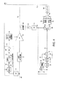
図3について、これら2つの特性を検出することより遅延誤差の方向を検出し、そして、このように検出された遅延の方向を使用してエンベロープ信号における遅延を制御するための例示的な実装が例示されている。 With respect to FIG. 3, an exemplary implementation for detecting the direction of the delay error by detecting these two characteristics and controlling the delay in the envelope signal using the direction of the delay thus detected is shown. Illustrated.
図3について、エンベロープ追跡を用いる増幅段の基本素子が例示されている。 With respect to FIG. 3, the basic elements of an amplification stage using envelope tracking are illustrated.
入力信号がライン60上に供給される。入力信号は、送信RF変調器ブロック8への入力を供給し、送信RF変調器ブロック8の出力は、電力増幅器10への入力として供給される。入力信号の増幅バージョンが、電力増幅器10の出力のライン62上で供給される。送信RF変調器ブロック8は、入力ライン60上の入力信号を変調することとなり、そのような入力信号をRF入力信号に変換する。
An input signal is provided on
エンベロープ追跡アーキテクチャに従って、ライン60上の入力信号は、エンベロープ回路14への入力を供給するAMブロック12にも供給される。既知の技法に従って、ライン15上のエンベロープ信号は、エンベロープ回路14によって生成され得、ライン15上のこのようにして生成されたエンベロープ信号は、電力増幅器10への変調された電源を供給するようにエンベロープ追跡変調器26を制御するために使用される。
In accordance with the envelope tracking architecture, the input signal on
エンベロープ追跡経路のエンベロープ追跡回路14は、遅延調整ブロック16、事前成形ゲイン及びオフセットブロック18、成形ブロック20、事後成形ゲイン及びオフセットブロック22、並びにDAC(デジタル/アナログ変換器)ブロック24を含み得る。
The envelope tracking path
改善に従って、遅延ブロック16は、以下により詳細に説明されるように、ライン66上の制御信号を受ける。これが、例示のための例示的な配列であること、及び、代替的又は追加的に、以下の技法に従って制御される可変遅延が、RF増幅器への入力経路に供給され得ることに留意されたい。
According to the improvement,
図3の追加の回路が、可変遅延ブロック16に加えられる遅延を制御するために、遅延誤差の方向を検出可能にする改善をもたらすために設けられる。
The additional circuitry of FIG. 3 is provided to provide an improvement that allows the direction of the delay error to be detected in order to control the delay applied to the
ライン60上の入力信号は、AMブロック52への入力として供給される。AMブロック52は、AMブロック12に対応し、単に、ライン60上の入力信号の振幅を表す信号をその出力として供給する。
The input signal on
AMブロック52の出力は、遅延ブロック54の入力に伝達され、遅延ブロック54の出力は、比較器58への第1の入力としてライン56上で供給される。比較器58への入力として供給されるライン56上の信号が、電力増幅器10の出力に依存して生成される比較器58の第2の入力に供給されるライン34上の信号と時間同期されるように、そのような段のライン60上の入力とライン62上の出力との間のエンベロープ追跡増幅回路におけるあらゆる遅延をシミュレートするために遅延ブロック54が設けられる。
The output of
電力増幅器10の出力に依存して生成される比較器58への第2の入力を供給するライン34上の信号は、復調器ブロック28、アナログ/デジタル変換器ブロック30、及びAMブロック32によって生成される。復調器ブロック28は、電力増幅器10の出力ライン62上でRF出力信号を検出し、その信号を復調する。復調された信号は、ブロック30によってデジタル形式に変換される。AMブロック32は、ブロック52に類似して、単に、ライン34上の信号として、ライン62上のRF出力信号のエンベロープ表現を提供するように動作する。
The signal on
ライン34上の信号は、電力制御の目的上、すでに供給されており、この配列のためにそのプロビジョンに関連付けられたオーバヘッドは存在しない。
The signal on
このように、比較器58は、第1の入力として、電力増幅段への入力信号を表すライン56上の信号を、そして電力増幅器段の出力信号を表すライン34上の信号を受ける。上述したように、遅延段54は、比較器58がそのような信号の瞬間値を効率的に比較するよう、そのような信号を同期するために設けられる。
Thus,
比較器58によって供給されるライン68上の比較器の出力は、電力増幅器段の出力と入力との間の比較を提供し、そして、電力増幅器段のゲインを示す指示を提供する。従って、ライン68上の信号は、「ゲイン値」信号である。ライン68上の比較器58の出力は、マルチプレクサ44への入力を形成する。
The output of the comparator on
電力増幅段への入力の大きさを表すライン56上の信号は、追加的に、閾値ブロック36及び差別化器ブロック38への入力として供給される。
A signal on
閾値ブロック36は、追加的に、ライン37上で最大電圧信号を、ライン39上で最小電圧信号を受け、ライン41上で出力信号を生成する。入力信号が特定の値(Vmax)よりも大きいか又は特定の値(Vmin)よりも小さい場合にのみ遅延の調整を制御するための回路が動作可能となることを確実にするために閾値ブロック36が設けられる。これは、この回路が、振幅情報が不正確であり得る入力信号の最小ピーク又は最大ピーク(最小値又は最大値)で動作可能になることを防ぐ。このように、閾値ブロック36は基本的に、入力信号の最大値及び最小値での回路の動作を無効にする。値Vmin及びVmaxのセッティングは、実装依存(implementation dependent)であり得、動的であり得る。
The
これらの閾値は、追加的に、AM/AMの拡散が最も広くなる小範囲の振幅レベルへと意志決定(decision making)を制限する。 These thresholds additionally limit decision making to a small range of amplitude levels where AM / AM spread is widest.
閾値は、入力信号というよりはむしろ出力信号に適用され得る。 The threshold can be applied to the output signal rather than the input signal.
図1に示されるように、閾値ブロック36は、ライン56上の入力信号を2つの閾値と比較し、ライン41上のその出力を使用して、入力信号振幅が2つの閾値間である場合にのみゲート42を有効にする。
As shown in FIG. 1, the
差別化器ブロック(differentiator block)38は、符号ブロック40に出力を供給し、符号ブロック40は、正又は負の何れかを示す符号をライン17上のその出力として供給する。
差別化器ブロック38及び符号ブロック40は、ライン56上の入力信号のスロープが増加型であるか減少型であるかに従って、ライン17上で正又は負の指示を生成するように動作する。
ゲート42は、ライン17上の符号ブロック40の出力を受け、これもまた、ライン41上の閾値ブロック36の出力によって有効/無効されるように制御され得る。有効にされると、ライン19上のゲート42の出力は、ライン17上で正又は負の指示となるだろう(符号ブロック40の出力に従って)。無効にされると、ゲート42の出力はゼロになるだろう。
ゲート42の出力は、マルチプレクサ44への制御入力を供給する。この制御入力は、増加型のスロープを有する入力信号を示す「+1」、減少型のスロープを有する入力信号を示す「−1」、又は、無効化(disablement)を示す「0」となるだろう。
The output of
マルチプレクサ44は、追加的に、更なる入力として、ライン68上の「ゲイン値」信号を受ける。
マルチプレクサ44は、平均ゲインブロック48への第1の出力信号及び平均ゲインブロック46への第2の出力信号という2つの出力信号のうちの1つを生成する。マルチプレクサの2つの出力は、ゲートの出力が正であること又は負であることに対応する。ゲート42の出力が正の場合、マルチプレクサ44は、ライン68上のゲイン値を平均ゲインブロック48に接続する。ゲート42の出力が負の場合、マルチプレクサ44は、ライン68上のゲイン値を平均ゲインブロック46に接続する。
平均ゲインブロック48及び46は、それぞれ、増加型及び減少型の入力スロープについての平均ゲイン値を含む。どちらのブロックの平均ゲイン値も、マルチプレクサが現在のゲイン値をブロック46、48のうちの1つに供給する場合、マルチプレクサの出力における現在のゲイン値を考慮するために更新される。このように、ブロック46及び48に記憶された平均ゲイン値は、それぞれ、立ち下がりスロープ及び立ち上がりスロープについての平均ゲインの移動平均(running average)とみなされ得る。好ましくはこの回路が最大値及び最小値で無効にされるという事実は、スロープの一部分を表す各スロープについての平均ゲインを供給する。
Average gain blocks 48 and 46 contain average gain values for increasing and decreasing input slopes, respectively. The average gain value of both blocks is updated to take into account the current gain value at the output of the multiplexer when the multiplexer supplies the current gain value to one of the
各平均ゲインブロックの出力は、ブロックの記憶された平均ゲイン値を供給する。 The output of each average gain block provides the stored average gain value of the block.
このように、有効にされると、平均ゲインブロック48及び46のうちの1つは、ライン68上でゲイン値を受けるだろう。ゲイン値を受ける平均ゲインブロック48及び46のうちの1つは、このゲイン値に従って、その保持された平均値を調整するだろう。この調整は、調整された平均値を供給するために、現在の平均値を考慮に入れるように平均値を更新することを備える。
Thus, when enabled, one of the average gain blocks 48 and 46 will receive a gain value on
ゲートの出力がゼロである場合、マルチプレクサは無効にされ、マルチプレクサの出力はいずれも設定されない。 If the gate output is zero, the multiplexer is disabled and none of the multiplexer outputs are set.
平均ゲインブロック48及び46の出力が、減算器/コンバイナ50によって合成される。このように、減算器/コンバイナは、平均ゲインブロック48及び46によって供給される平均ゲイン値を合成する。
The outputs of the average gain blocks 48 and 46 are combined by a subtracter /
図示の例では、減算器/コンバイナは、立ち下がりスロープ上の平均ゲイン(又は、移動平均)から、立ち上がりスロープ上の平均ゲイン(又は、移動平均ゲイン)を減算する。図1を参照すると、例えば、これは、スロープ102の平均ゲインが、スロープ104の平均ゲインから減算されることを意味する。
In the example shown, the subtracter / combiner subtracts the average gain (or moving average gain) on the rising slope from the average gain (or moving average) on the falling slope. With reference to FIG. 1, for example, this means that the average gain of the
この減算は、2つの平均値間の(最大値及び最小値前後での無効化によって決定する閾値内の)差分を示す指示を提供し、それは、その差分の方向(正又は負)を含む。一実施形態では、この方向は十分な情報であり、この差分を最小化するためにどの方向に遅延が調整されるべきかについての情報を伝える。別の実施形態では、遅延は、差分のサイズぶん、その方向に調整される。差分は、誤差、及び遅延が調整されるべき量を表す。 This subtraction provides an indication of the difference between two average values (within a threshold determined by invalidation around the maximum and minimum values), which includes the direction of the difference (positive or negative). In one embodiment, this direction is sufficient information to convey information about which direction the delay should be adjusted to minimize this difference. In another embodiment, the delay is adjusted in that direction by the size of the difference. The difference represents the error and the amount by which the delay is to be adjusted.
減算器/比較器の出力は、入力信号がエンベロープ信号に先行するか遅行するかを示す。この決定を行うために、入力信号とエンベロープ信号のタイミングを具体的に比較することが必ずしも必要ではないことと、例えば、入力信号とエンベロープ信号のタイミングを表す2つの信号を比較することが十分であることとが理解され得る。 The output of the subtracter / comparator indicates whether the input signal precedes or delays the envelope signal. In order to make this determination, it is not always necessary to specifically compare the timing of the input signal and the envelope signal, and for example, it is sufficient to compare two signals representing the timing of the input signal and the envelope signal. It can be understood that there is.
誤差が無い場合、例えば、誤差がゼロに減らされると、ブロック46及び48に記憶されているアベレージ値間の差分はゼロになるだろう。
If there is no error, for example, if the error is reduced to zero, the difference between the average values stored in
説明される例では、入力信号とエンベロープ信号との間の遅延差を表す誤差信号が特定の方法で決定されるが、本発明はこれに限られない。例えば、図1を参照すると、立ち上がり又は負のスロープ(スロープ102又は104)上の瞬間ゲイン値(又は、平均ゲイン値)が、合計アベレージゲイン(スロープ100によって表される)と比較され、スロープ102又は104上の値の差分(又は、平均値)がスロープ100上の合計平均値と比較される。これは、同様に、誤差の方向及び/又は値を供給する。誤差が無い場合、例えば、誤差がゼロに減らされると、ブロック46及び48に記憶されているアベレージ値と、トータル平均誤差(立ち上がりスロープ及び立ち下がりスロープ上の)との差分はゼロになるだろう。
In the example described, the error signal representing the delay difference between the input signal and the envelope signal is determined in a particular way, but the invention is not limited to this. For example, referring to FIG. 1, the instantaneous gain value (or average gain value) on a rising or negative slope (
このように、コンバイナ50の出力は、2つの平均ゲインブロック48及び46によって保持される値の組み合わせを表す。コンバイナ50の出力は、ダンピングブロック64への入力として供給される。
Thus, the output of the
ダンピングブロック64の出力は、ライン66上で制御信号を形成し、遅延ブロック16に制御信号を供給する。ライン66上の制御信号は、遅延ブロック16の遅延に対してなされるべき調整を示す。
The output of damping
図3を参照して説明された上記配列は、エンベロープ経路においてゲインを調整又は制御するためにライン66上のゲイン制御信号が信号を供給する本発明を実装するための例示的な実装を提供する。
The above arrangement described with reference to FIG. 3 provides an exemplary implementation for implementing the present invention in which a gain control signal on
図4を参照して、遅延誤差の方向を検出するための代替的かつ例示的な実装が例示されている。図4、及びすべての図では、同様の参照番号が、複数の図の間で機能的に等価である素子を識別するために使用される。 With reference to FIG. 4, an alternative exemplary implementation for detecting the direction of delay error is illustrated. In FIG. 4 and all the figures, similar reference numerals are used to identify elements that are functionally equivalent among the figures.
図4について、図1の配列に類似した配列が一般に示されるが、処理は全体的に、ライン62上の電力増幅器10の出力信号に基づく。
With respect to FIG. 4, an arrangement similar to that of FIG. 1 is generally shown, but the processing is generally based on the output signal of
復調された出力信号は、図3の配列にあるようにライン34上で生成される。ライン34上のこの信号は、差別化器ブロック38及び閾値ブロック36への入力を直接的に供給し、追加的に、マルチプレクサ44に入力される値を直接的に供給する。閾値ブロック36、差別化器38、符号ブロック40、及びゲート42は、正(+1)、負(−1)、又はゼロ(0)のいずれかであるマルチプレクサ44の制御入力へのライン19上の信号を生成するために、図3に関して説明されたように動作する。
The demodulated output signal is generated on
マルチプレクサ44の正及び負の出力は、それぞれ、図3の平均ゲインブロック48及び平均ゲインブロック46というよりもむしろ、平均振幅ブロック70及び平均振幅ブロック72に接続される。この例では、平均振幅ブロック70及び72の各々が、それぞれ、ライン62上の出力信号の平均振幅に対応する値を保持する。平均振幅ブロック70又は72において保持される平均振幅値は、ライン34上の値を考慮するように平均値を調整することによって更新される。この例となる実装における差分又は誤差の決定の動作は、図3のものと同じである。立ち上がり又は立ち下がりエッジにおける平均値はそれぞれ、立ち下り又は立ち上がりエッジにおける平均値と比較され、差分は、誤差の方向及びサイズを表し、情報のそれらのピースのうちの一方又は両方が、入力経路又はエンベロープ経路の何れかにおける遅延を制御するために使用され得る。
The positive and negative outputs of
平均振幅ブロック70及び72の出力は、遅延ブロック16にライン66上で可変ゲイン制御信号を供給するダンピングブロック64への入力を供給するコンバイナ50への入力として供給される。
The outputs of the average amplitude blocks 70 and 72 are provided as inputs to a
このように、図4の配列は、信号のスロープと、遅延の誤差とを決定するために電力増幅器出力を使用することが可能であることを例示する。 Thus, the arrangement of FIG. 4 illustrates that the power amplifier output can be used to determine the slope of the signal and the delay error.
図5について、遅延誤差の方向を検出するための更なる例示的な実装が例示されている。 With respect to FIG. 5, a further exemplary implementation for detecting the direction of delay error is illustrated.
図5を参照すると、ライン56上の遅延ブロックの出力が、図3の配列にあるように、入力として閾値ブロック36及び差別化器ブロック38に供給され、図3の配列にあるように、閾値ブロック36、差別化器ブロック38、符号ブロック40、及びゲート42は、ライン19上の信号を生成するように動作する。マルチプレクサ44のために入力される値は、出力62から復調される信号34によって直接的に供給される。マルチプレクサ44に入力される値を生成することに加え、ライン34上の信号はまた、他のアプリケーション要件に従った電力制御にも利用可能である。
Referring to FIG. 5, the output of the delay block on
図4の配列にあるように、誤差が無い場合の配列では、例えば、誤差がゼロに減らされると、ブロック46及び48に記憶されたアベレージ値間の差分はゼロになるだろう。
As in the array of FIG. 4, in the case of no error, for example, if the error is reduced to zero, the difference between the average values stored in
図5の平均振幅ブロック70及び平均振幅ブロック72は、増加型のスロープ又は減少型のスロープの何れかの上の出力信号の平均振幅が、ライン34上の値に依存して更新されるように、マルチプレクサ44の出力に設けられる。
The
このように、遅延制御信号は、上述された技法に従ってライン66上で生成される。
Thus, the delay control signal is generated on
上述された配列は、限定的でも徹底的でもない発明を実装するための技法を例示する。 The above-described arrangements illustrate techniques for implementing the invention that are not limiting or exhaustive.
一般に、瞬間信号を得ることができるAMフィードバック受信機を有する送信機を提供することが必要とされる。LTE実装では、瞬間信号を得るためのサンプルレートは、LTE信号を得るのに十分高い必要がある。得られるサンプルの長さ又はサイズは重要ではない。従って、瞬間信号を得るためのRAMは、実装に十分なサンプルレートを有する必要があるが、RAMの長さ/サイズは重要ではない。 In general, it is necessary to provide a transmitter with an AM feedback receiver that can obtain an instantaneous signal. In LTE implementations, the sample rate for obtaining the instantaneous signal needs to be high enough to obtain the LTE signal. The length or size of the resulting sample is not critical. Therefore, the RAM for obtaining the instantaneous signal needs to have a sufficient sample rate for mounting, but the length / size of the RAM is not important.
例示的な実装では、エンベロープ追跡増幅段のゲイン調整は、エンベロープ追跡増幅段のゲイン誤差を算出することによって決定され得る。 In an exemplary implementation, the gain adjustment of the envelope tracking amplification stage may be determined by calculating the gain error of the envelope tracking amplification stage.
代替的な実装では、遅延ブロック16の遅延セッティングは、ゲイン誤差の統合に依存して調整され得る。ダンピングブロック64によって供給されるダンピングは、ACLRが劣化しないように設定され得る。
In an alternative implementation, the delay setting of
図に示された例示的な解決策は、閉ループシステムを提供する際に有利であり、従って、これは、温度変化を追跡するであろう。工場での遅延較正は必要ではなく、開ループ遅延補正が必要とされない。 The exemplary solution shown in the figure is advantageous in providing a closed loop system, so this will track temperature changes. Factory delay calibration is not required and open loop delay compensation is not required.
本発明は、本明細書において、特定の利点のある実施形態及び例示的な実装を参照して説明されている。本発明は、そのような実施形態及び実装の任意の態様の任意の詳細に限定されるわけではない。本発明の範囲は、添付の特許請求の範囲によって定義される。 The present invention has been described herein with reference to certain advantageous embodiments and exemplary implementations. The invention is not limited to any details of any aspects of such embodiments and implementations. The scope of the present invention is defined by the appended claims.
Claims (14)
Applications Claiming Priority (3)
| Application Number | Priority Date | Filing Date | Title |
|---|---|---|---|
| GB1309236.6 | 2013-05-22 | ||
| GB1309236.6A GB2514388A (en) | 2013-05-22 | 2013-05-22 | Delay adjustment |
| PCT/EP2014/060581 WO2014187918A1 (en) | 2013-05-22 | 2014-05-22 | Delay adjustment |
Publications (2)
| Publication Number | Publication Date |
|---|---|
| JP2016519545A true JP2016519545A (en) | 2016-06-30 |
| JP2016519545A5 JP2016519545A5 (en) | 2017-06-15 |
Family
ID=48747171
Family Applications (1)
| Application Number | Title | Priority Date | Filing Date |
|---|---|---|---|
| JP2016514418A Pending JP2016519545A (en) | 2013-05-22 | 2014-05-22 | Delay adjustment |
Country Status (6)
| Country | Link |
|---|---|
| US (1) | US10075134B2 (en) |
| EP (1) | EP3000173A1 (en) |
| JP (1) | JP2016519545A (en) |
| CN (1) | CN105229920B (en) |
| GB (1) | GB2514388A (en) |
| WO (1) | WO2014187918A1 (en) |
Families Citing this family (12)
| Publication number | Priority date | Publication date | Assignee | Title |
|---|---|---|---|---|
| US11108363B2 (en) | 2018-09-04 | 2021-08-31 | Qorvo Us, Inc. | Envelope tracking circuit and related power amplifier apparatus |
| US10819287B2 (en) | 2018-10-19 | 2020-10-27 | Qorvo Us, Inc. | Multi-voltage generation circuit and related envelope tracking amplifier apparatus |
| US11108359B2 (en) | 2018-10-19 | 2021-08-31 | Qorvo Us, Inc. | Multi-amplifier envelope tracking circuit and related apparatus |
| US11057012B2 (en) | 2018-10-19 | 2021-07-06 | Qorvo Us, Inc. | Distributed envelope tracking amplifier circuit and related apparatus |
| US11146213B2 (en) | 2019-01-15 | 2021-10-12 | Qorvo Us, Inc. | Multi-radio access technology envelope tracking amplifier apparatus |
| US10992264B2 (en) | 2019-03-13 | 2021-04-27 | Qorvo Us, Inc. | Envelope tracking circuit and related apparatus |
| US11088658B2 (en) | 2019-03-13 | 2021-08-10 | Qorvo Us, Inc. | Envelope tracking amplifier apparatus |
| US11139780B2 (en) | 2019-04-24 | 2021-10-05 | Qorvo Us, Inc. | Envelope tracking apparatus |
| US11038464B2 (en) * | 2019-05-30 | 2021-06-15 | Qorvo Us, Inc. | Envelope tracking amplifier apparatus |
| US11323075B2 (en) | 2019-05-30 | 2022-05-03 | Qorvo Us, Inc. | Envelope tracking amplifier apparatus |
| US20230069759A1 (en) * | 2021-08-31 | 2023-03-02 | Viavi Solutions Inc. | Hybrid digital-analog automatic level control (alc) using vector signal generators (vsg) |
| US11906992B2 (en) | 2021-09-16 | 2024-02-20 | Qorvo Us, Inc. | Distributed power management circuit |
Citations (2)
| Publication number | Priority date | Publication date | Assignee | Title |
|---|---|---|---|---|
| JP2007189438A (en) * | 2006-01-12 | 2007-07-26 | Fujitsu Ltd | Timing adjusting device and timing adjusting method |
| JP2010226198A (en) * | 2009-03-19 | 2010-10-07 | Fujitsu Ltd | Power amplifying device and power amplifying method |
Family Cites Families (10)
| Publication number | Priority date | Publication date | Assignee | Title |
|---|---|---|---|---|
| EP1548949A4 (en) * | 2002-10-03 | 2009-06-24 | Panasonic Corp | Transmitting method and transmitter apparatus |
| JP3985649B2 (en) | 2002-10-03 | 2007-10-03 | 松下電器産業株式会社 | Transmission method and transmission apparatus |
| JP4230238B2 (en) * | 2003-02-06 | 2009-02-25 | パナソニック株式会社 | Transmitting apparatus and adjustment method thereof |
| US7372917B2 (en) * | 2004-08-25 | 2008-05-13 | Broadcom Corporation | Digital algorithm for on-line ACPR optimization in polar RF transmitters |
| EP2226932B1 (en) | 2009-03-02 | 2013-10-16 | Alcatel Lucent | Method for amplifying a signal by a power amplifier, power amplifier system, device, computer program product, and digital storage medium thereof |
| JP2010219326A (en) | 2009-03-17 | 2010-09-30 | Elpida Memory Inc | Semiconductor memory device and method of manufacturing the same |
| GB2479579B (en) | 2010-04-15 | 2017-12-06 | Snaptrack Inc | Timing alignment for modulated supply |
| JP5655654B2 (en) * | 2011-03-18 | 2015-01-21 | 富士通株式会社 | Amplifier |
| JP5638132B2 (en) | 2011-06-03 | 2014-12-10 | 京セラ株式会社 | Transmitter and signal processing method |
| CN107171645A (en) * | 2012-03-04 | 2017-09-15 | 匡坦斯公司 | Power amplifier system and delay calibration method |
-
2013
- 2013-05-22 GB GB1309236.6A patent/GB2514388A/en not_active Withdrawn
-
2014
- 2014-05-22 US US14/892,501 patent/US10075134B2/en active Active
- 2014-05-22 CN CN201480028795.5A patent/CN105229920B/en active Active
- 2014-05-22 WO PCT/EP2014/060581 patent/WO2014187918A1/en active Application Filing
- 2014-05-22 JP JP2016514418A patent/JP2016519545A/en active Pending
- 2014-05-22 EP EP14730443.0A patent/EP3000173A1/en not_active Ceased
Patent Citations (2)
| Publication number | Priority date | Publication date | Assignee | Title |
|---|---|---|---|---|
| JP2007189438A (en) * | 2006-01-12 | 2007-07-26 | Fujitsu Ltd | Timing adjusting device and timing adjusting method |
| JP2010226198A (en) * | 2009-03-19 | 2010-10-07 | Fujitsu Ltd | Power amplifying device and power amplifying method |
Also Published As
| Publication number | Publication date |
|---|---|
| GB201309236D0 (en) | 2013-07-03 |
| US10075134B2 (en) | 2018-09-11 |
| US20160094185A1 (en) | 2016-03-31 |
| WO2014187918A1 (en) | 2014-11-27 |
| GB2514388A (en) | 2014-11-26 |
| EP3000173A1 (en) | 2016-03-30 |
| CN105229920A (en) | 2016-01-06 |
| CN105229920B (en) | 2019-05-10 |
Similar Documents
| Publication | Publication Date | Title |
|---|---|---|
| JP2016519545A (en) | Delay adjustment | |
| US9793858B2 (en) | Transfer function regulation | |
| US8461928B2 (en) | Constant-gain power amplifier | |
| US9166830B2 (en) | Systems and methods utilizing adaptive envelope tracking | |
| EP1382115B1 (en) | Automatic optimization of linearity for envelope feedback rf amplifier linearization | |
| US8014735B2 (en) | RF power amplifier controlled by estimated distortion level of output signal of power amplifier | |
| US7493091B2 (en) | Transmission circuit and communication device | |
| JP4863729B2 (en) | Distortion compensation apparatus and distortion compensation method | |
| US20090256630A1 (en) | Method of power amplifier predistortion adaptation using compression detection | |
| JP2002100940A (en) | Distortion compensation amplifier | |
| US20130194037A1 (en) | Power amplifier, radio-frequency power amplification device, and amplification control method | |
| KR20100069454A (en) | Method and apparatus for enhancing performance of a doherty power amplifier in a communication system | |
| US8514018B2 (en) | Signal alignment for envelope tracking system | |
| JP2010278992A (en) | Rf amplification apparatus | |
| US8243854B2 (en) | Amplitude control circuit, polar modulation transmission circuit and polar modulation method | |
| US8699976B2 (en) | Transmitter with hybrid closed loop power control | |
| US9184704B2 (en) | Timing alignment for power amplifier | |
| US8514969B2 (en) | Amplitude control circuit, polar modulation transmission circuit, and polar modulation method | |
| KR100976863B1 (en) | Apparatus and method for compensating nonlinear distortion of power amplifier | |
| JP2005150814A (en) | Method and apparatus of compensating non-linear distortion | |
| KR20100082958A (en) | Apparatus and method for controlling a bias of a high power amplifier | |
| CN103428133A (en) | Predistortion temperature compensation device and method, predistorter and transmitter |
Legal Events
| Date | Code | Title | Description |
|---|---|---|---|
| A521 | Request for written amendment filed |
Free format text: JAPANESE INTERMEDIATE CODE: A523 Effective date: 20170426 |
|
| A621 | Written request for application examination |
Free format text: JAPANESE INTERMEDIATE CODE: A621 Effective date: 20170426 |
|
| A977 | Report on retrieval |
Free format text: JAPANESE INTERMEDIATE CODE: A971007 Effective date: 20180626 |
|
| A131 | Notification of reasons for refusal |
Free format text: JAPANESE INTERMEDIATE CODE: A131 Effective date: 20180703 |
|
| A521 | Request for written amendment filed |
Free format text: JAPANESE INTERMEDIATE CODE: A523 Effective date: 20181001 |
|
| A131 | Notification of reasons for refusal |
Free format text: JAPANESE INTERMEDIATE CODE: A131 Effective date: 20181106 |
|
| A02 | Decision of refusal |
Free format text: JAPANESE INTERMEDIATE CODE: A02 Effective date: 20190604 |