JP6166457B2 - Envelope tracking system with internal power amplifier characterization - Google Patents
Envelope tracking system with internal power amplifier characterization Download PDFInfo
- Publication number
- JP6166457B2 JP6166457B2 JP2016502142A JP2016502142A JP6166457B2 JP 6166457 B2 JP6166457 B2 JP 6166457B2 JP 2016502142 A JP2016502142 A JP 2016502142A JP 2016502142 A JP2016502142 A JP 2016502142A JP 6166457 B2 JP6166457 B2 JP 6166457B2
- Authority
- JP
- Japan
- Prior art keywords
- power amplifier
- supply voltage
- amplifier system
- amplitude
- characterization
- Prior art date
- Legal status (The legal status is an assumption and is not a legal conclusion. Google has not performed a legal analysis and makes no representation as to the accuracy of the status listed.)
- Active
Links
Images


Classifications
-
- H—ELECTRICITY
- H03—ELECTRONIC CIRCUITRY
- H03F—AMPLIFIERS
- H03F1/00—Details of amplifiers with only discharge tubes, only semiconductor devices or only unspecified devices as amplifying elements
- H03F1/02—Modifications of amplifiers to raise the efficiency, e.g. gliding Class A stages, use of an auxiliary oscillation
- H03F1/0205—Modifications of amplifiers to raise the efficiency, e.g. gliding Class A stages, use of an auxiliary oscillation in transistor amplifiers
- H03F1/0211—Modifications of amplifiers to raise the efficiency, e.g. gliding Class A stages, use of an auxiliary oscillation in transistor amplifiers with control of the supply voltage or current
- H03F1/0216—Continuous control
- H03F1/0222—Continuous control by using a signal derived from the input signal
-
- H—ELECTRICITY
- H03—ELECTRONIC CIRCUITRY
- H03F—AMPLIFIERS
- H03F3/00—Amplifiers with only discharge tubes or only semiconductor devices as amplifying elements
- H03F3/189—High frequency amplifiers, e.g. radio frequency amplifiers
-
- H—ELECTRICITY
- H03—ELECTRONIC CIRCUITRY
- H03F—AMPLIFIERS
- H03F1/00—Details of amplifiers with only discharge tubes, only semiconductor devices or only unspecified devices as amplifying elements
- H03F1/02—Modifications of amplifiers to raise the efficiency, e.g. gliding Class A stages, use of an auxiliary oscillation
- H03F1/0205—Modifications of amplifiers to raise the efficiency, e.g. gliding Class A stages, use of an auxiliary oscillation in transistor amplifiers
- H03F1/0211—Modifications of amplifiers to raise the efficiency, e.g. gliding Class A stages, use of an auxiliary oscillation in transistor amplifiers with control of the supply voltage or current
- H03F1/0216—Continuous control
- H03F1/0222—Continuous control by using a signal derived from the input signal
- H03F1/0227—Continuous control by using a signal derived from the input signal using supply converters
-
- H—ELECTRICITY
- H03—ELECTRONIC CIRCUITRY
- H03F—AMPLIFIERS
- H03F1/00—Details of amplifiers with only discharge tubes, only semiconductor devices or only unspecified devices as amplifying elements
- H03F1/02—Modifications of amplifiers to raise the efficiency, e.g. gliding Class A stages, use of an auxiliary oscillation
- H03F1/0205—Modifications of amplifiers to raise the efficiency, e.g. gliding Class A stages, use of an auxiliary oscillation in transistor amplifiers
- H03F1/0211—Modifications of amplifiers to raise the efficiency, e.g. gliding Class A stages, use of an auxiliary oscillation in transistor amplifiers with control of the supply voltage or current
- H03F1/0216—Continuous control
- H03F1/0233—Continuous control by using a signal derived from the output signal, e.g. bootstrapping the voltage supply
- H03F1/0238—Continuous control by using a signal derived from the output signal, e.g. bootstrapping the voltage supply using supply converters
-
- H—ELECTRICITY
- H03—ELECTRONIC CIRCUITRY
- H03F—AMPLIFIERS
- H03F1/00—Details of amplifiers with only discharge tubes, only semiconductor devices or only unspecified devices as amplifying elements
- H03F1/32—Modifications of amplifiers to reduce non-linear distortion
-
- H—ELECTRICITY
- H03—ELECTRONIC CIRCUITRY
- H03F—AMPLIFIERS
- H03F3/00—Amplifiers with only discharge tubes or only semiconductor devices as amplifying elements
- H03F3/189—High frequency amplifiers, e.g. radio frequency amplifiers
- H03F3/19—High frequency amplifiers, e.g. radio frequency amplifiers with semiconductor devices only
-
- H—ELECTRICITY
- H03—ELECTRONIC CIRCUITRY
- H03F—AMPLIFIERS
- H03F3/00—Amplifiers with only discharge tubes or only semiconductor devices as amplifying elements
- H03F3/20—Power amplifiers, e.g. Class B amplifiers, Class C amplifiers
- H03F3/21—Power amplifiers, e.g. Class B amplifiers, Class C amplifiers with semiconductor devices only
-
- H—ELECTRICITY
- H03—ELECTRONIC CIRCUITRY
- H03F—AMPLIFIERS
- H03F3/00—Amplifiers with only discharge tubes or only semiconductor devices as amplifying elements
- H03F3/20—Power amplifiers, e.g. Class B amplifiers, Class C amplifiers
- H03F3/24—Power amplifiers, e.g. Class B amplifiers, Class C amplifiers of transmitter output stages
-
- H—ELECTRICITY
- H03—ELECTRONIC CIRCUITRY
- H03F—AMPLIFIERS
- H03F2200/00—Indexing scheme relating to amplifiers
- H03F2200/102—A non-specified detector of a signal envelope being used in an amplifying circuit
-
- H—ELECTRICITY
- H03—ELECTRONIC CIRCUITRY
- H03F—AMPLIFIERS
- H03F2200/00—Indexing scheme relating to amplifiers
- H03F2200/451—Indexing scheme relating to amplifiers the amplifier being a radio frequency amplifier
Landscapes
- Engineering & Computer Science (AREA)
- Power Engineering (AREA)
- Physics & Mathematics (AREA)
- Nonlinear Science (AREA)
- Amplifiers (AREA)
- Transmitters (AREA)
Description
関連出願への相互参照
この出願は2013年3月15日に提出された、米国仮特許出願第61/800,350号の恩恵を主張し、その全体をここに引用により援用する。
This application claims the benefit of US Provisional Patent Application No. 61 / 800,350, filed Mar. 15, 2013, which is hereby incorporated by reference in its entirety.
背景
開示の分野
この開示は、一般的に、包絡線追跡電力増幅器システムに関し、より具体的には、改善された特性を伴う包絡線追跡電力増幅器システムに関する。
BACKGROUND Field of the Disclosure This disclosure relates generally to envelope tracking power amplifier systems, and more specifically to envelope tracking power amplifier systems with improved characteristics.
関連技術の説明
包絡線追跡(ET)システムは、携帯電話において用いられるセルラー方式無線受信機におけるような、電力効率が重要である無線受信機の無線周波数(RF)送信機部において見られ得る。典型的なETシステムは、変調の振幅を追跡する動的に変化する供給電圧を電力増幅器(PA)に供給する可変電源を含む。そのようなETシステムの目的は、低いヘッドルームでPAを動作させることにより、電力効率を改善することである。
2. Description of Related Art Envelope tracking (ET) systems can be found in the radio frequency (RF) transmitter section of radio receivers where power efficiency is important, such as in cellular radio receivers used in mobile phones. A typical ET system includes a variable power supply that supplies a power amplifier (PA) with a dynamically changing supply voltage that tracks the amplitude of the modulation. The purpose of such an ET system is to improve power efficiency by operating the PA with low headroom.
供給電圧レベルは、供給電圧に対する値に対する振幅を参照するルックアップテーブルで判断することが可能である。図7はルックアップテーブルに対して利用可能な選択の性質を示す。例として、22dBmのPA出力電力に対応する振幅については、ルックアップテーブルは、1.2Vから5Vまでの範囲のPA供給電圧値を含んでもよい。この値の選択はPA効率と線形性との間の十分なバランスを与えるよう設定されてもよい。PA供給電圧の設定が低すぎる場合、PAはより低いヘッドルーム、およびしたがってより高い効率で動作するが、しかしより高い歪みを伴う。逆に、PA供給電圧の設定が高すぎる場合、PAはより高いヘッドルーム、およびしたがってより低い効率で動作するが、さらなるヘッドルームが、より低い歪みレベルを可能にする。 The supply voltage level can be determined with a look-up table that references the amplitude for the value for the supply voltage. FIG. 7 shows the nature of the choices available for the lookup table. As an example, for an amplitude corresponding to a 22 dBm PA output power, the lookup table may include PA supply voltage values ranging from 1.2V to 5V. The choice of this value may be set to give a sufficient balance between PA efficiency and linearity. If the PA supply voltage is set too low, the PA operates with lower headroom, and therefore higher efficiency, but with higher distortion. Conversely, if the PA supply voltage is set too high, the PA will operate with higher headroom and therefore lower efficiency, but additional headroom will allow for lower distortion levels.
ルックアップテーブルに対する値は、典型的には、工場で、典型的な条件下で典型的な無線受信機装置上で典型的なPA上での特徴付けを通して判断される。次いで、この初期の値の集合は、他のETシステムにコピーされる。しかしながら、他のETシステムの実際の動作中に、PAは、PAプロセスおよび製造公差、電源回路ばらつき、環境要因、温度、動作周波数変調形式およびアンテナ不整合などのような要因に依って、典型的なPAの特徴付け中のそれらとは異なった特性を示すかもしれない。したがって、初期の値の集合は、電力効率と歪みとの正しいバランスでPAを動作させないかもしれない。 The values for the look-up table are typically determined through characterization on a typical PA on a typical radio receiver device under typical conditions at the factory. This initial set of values is then copied to the other ET system. However, during the actual operation of other ET systems, PAs are typically subject to factors such as PA process and manufacturing tolerances, power supply circuit variations, environmental factors, temperature, operating frequency modulation type and antenna mismatch etc. May show different properties than those in the characterization of new PAs. Thus, the initial set of values may not operate the PA with the correct balance of power efficiency and distortion.
概要
この開示の実施の形態は、それ自体の局所的な特徴付け情報を生成するRF・PAシステムを含む。次いで、RF・PAシステムは特徴付け情報を用いて、PAへの供給電圧を制御する。その結果、RF・PAシステムは、電力効率と歪みとの間の所望のバランスをより正確に達成する態様で供給電圧を制御することが可能である。
Overview Embodiments of this disclosure include an RF PA system that generates its own local characterization information. The RF / PA system then uses the characterization information to control the supply voltage to the PA. As a result, the RF PA system can control the supply voltage in a manner that more accurately achieves the desired balance between power efficiency and distortion.
一実施の形態では、RF・PAシステムは、RF入力信号からRF出力信号を生成するためにPAを含み、PAは供給電圧によって電力を供給される。特徴付けブロックは、RF・PAシステムの1つ以上の動作条件(たとえば温度、動作周波数、変調フォーマット、アンテナ不整合など)の複数のレベルに対して、供給電圧とRF・PAシステムの性能(たとえば利得、電力効率、歪み、受信バンドノイズ)との間の関係に対応する特徴付け情報を生成する。振幅推定部ブロックは、RF入力信号の振幅を推定する。供給制御ブロックは、特徴付け情報およびRF入力信号の振幅に基いて、供給電圧を制御するための供給電圧制御信号を生成する。 In one embodiment, the RF PA system includes a PA to generate an RF output signal from an RF input signal, and the PA is powered by a supply voltage. The characterization block may provide supply voltage and RF / PA system performance (eg, for multiple levels of one or more operating conditions of the RF / PA system (eg, temperature, operating frequency, modulation format, antenna mismatch, etc.) Characterization information corresponding to the relationship between (gain, power efficiency, distortion, received band noise) is generated. The amplitude estimator block estimates the amplitude of the RF input signal. The supply control block generates a supply voltage control signal for controlling the supply voltage based on the characterization information and the amplitude of the RF input signal.
一実施の形態では、RF・PAシステムにおける動作の方法は、RF・PAシステムにおいて、RF・PAシステムの動作条件の複数のレベルに対して、PAへの供給電圧とPAの性能と間の関係に対応する特徴付け情報を生成することを含み、PAはRF入力信号に基いてRF出力信号を生成し;この方法はさらに、RF・PAシステムにおいて、RF入力信号の振幅を推定することと;RF・PAシステムにおいて、特徴付け情報およびRF入力信号の振幅に基いて、PAへの供給電圧を制御するための供給電圧制御信号を生成することとを含む。 In one embodiment, a method of operation in an RF PA system is the relationship between the supply voltage to the PA and the PA performance for multiple levels of operating conditions in the RF PA system. Generating a characterization information corresponding to, wherein the PA generates an RF output signal based on the RF input signal; the method further includes estimating an amplitude of the RF input signal in the RF PA system; Generating a supply voltage control signal for controlling the supply voltage to the PA based on the characterization information and the amplitude of the RF input signal.
明細書に記載される特徴および利点はすべて包含的ではなく、特に、多くのさらなる特徴および利点が、図面、明細書および特許請求の範囲に鑑み、当業者には明らかになる。さらに、明細書において用いられる文言は、主に読みやすさおよび指示上の目的に対して選択され、発明の主題を輪郭づけるかまたは限定するためには選択されなかったかもしれないことが注記されるべきである。 All features and advantages described in the specification are not inclusive, and many additional features and advantages will be apparent to those skilled in the art in view of the drawings, specification, and claims. Furthermore, it is noted that the language used in the specification was selected primarily for readability and instructional purposes and may not have been selected to outline or limit the subject matter of the invention. Should be.
図面の簡単な説明
この発明の実施の形態の教示は、添付の図面と関連して以下の詳細な記載を考慮することにより容易に理解され得る。
BRIEF DESCRIPTION OF THE DRAWINGS The teachings of the embodiments of the present invention can be readily understood by considering the following detailed description in conjunction with the accompanying drawings, in which:
詳細な記載
この開示のいくつかの実施の形態がここで詳細に言及され、それらの例は添付の図に示される。可能な場合は、類似または同様の参照番号が図において用いられ得、類似または同様の機能を示してもよいことに注意されたい。図は、例示のみの目的のためにこの発明の実施の形態を示す。当業者は、ここに示される構造および方法の代替的実施の形態がここに記載されるこの発明の原理から逸脱せずに用いられてもよいことを、以下の記載から容易に認識する。
Detailed Description Reference will now be made in detail to certain embodiments of the disclosure, examples of which are illustrated in the accompanying drawings. It should be noted that where possible, similar or similar reference numerals may be used in the figures to indicate similar or similar functions. The figure shows an embodiment of the invention for illustrative purposes only. Those skilled in the art will readily recognize from the following description that alternative embodiments of the structures and methods shown herein may be used without departing from the principles of the invention described herein.
この開示の実施の形態は、RF・PAシステムそれ自体の内部からのフィードバックを用いてそれ自体の局所的な特徴付け情報を生成するRF・PAシステムを含む。次いで、RF・PAシステムは特徴付け情報を用いて、PAへの供給電圧を制御する。その結果、RF・PAシステムは、電力効率と歪みとの間の所望のバランスをより正確に達成する態様で供給電圧を制御することが可能である。一実施の形態では、RF・PAシステムはRF・PAシステムの通常の送信動作中にRF・PAシステムの動作を中断せずに特徴付けを実行することが可能である。他の実施の形態では、RF・PAシステムはオフライン較正モード中に特徴付けを実行することが可能である。 Embodiments of this disclosure include an RF • PA system that uses its own internal feedback to generate its own local characterization information. The RF / PA system then uses the characterization information to control the supply voltage to the PA. As a result, the RF PA system can control the supply voltage in a manner that more accurately achieves the desired balance between power efficiency and distortion. In one embodiment, the RF / PA system can perform characterization without interrupting the operation of the RF / PA system during normal transmission operation of the RF / PA system. In other embodiments, the RF PA system can perform characterization during an off-line calibration mode.
図1は、この開示の実施の形態に従うRF・PAシステムを示す。RF・PAシステムは、送信変調部10と振幅推定部13とRFアップコンバータ2と電力増幅器(PA)3とアンテナ4とデュプレクサ5とフィードバック受信部24と特徴付けブロック102と特徴付け情報テーブル33と供給制御ブロック104と包絡線追跡(ET)電源8を含む。図において示されるブロックの各々は、回路系または回路系とソフトウェアとの組合せにおいて実現することが可能である。RF・PAシステムは、携帯電話、モバイルホットスポット、タブレットコンピュータ、または無線通信をサポートする任意の他のタイプのコンピューティング装置において見出され得る。RF・PAシステムは、遠隔装置への無線信号の送信のために3G、4Gおよびロングタームエボリューション(LTE)などのような異なる無線伝送規格をサポートすることが可能である。図を単純化するために、送出信号の送信のための送信経路のみが図1に示され、入来信号を受信するための受信経路は図1から省略される。
FIG. 1 illustrates an RF PA system according to an embodiment of this disclosure. The RF / PA system includes a
送信変調部10は、遠隔装置に無線信号として送信されるべき所望の情報を含むデジタルベースバンド信号1を生成する。デジタルベースバンド信号1はRFアップコンバータ2によって変換されて、特定のRF搬送周波数で動作するRF入力信号17を生成する。可変利得RFアップコンバータ2は、可変利得ドライバが後に続くアップコンバートミキサ回路の組によって実現されてもよい。可変利得RFアップコンバータ2の利得は、送信変調部10によって利得制御信号16を介して制御される。可変利得RFアップコンバータ2の利得は、送信電力制御、および送信経路におけるノイズ最適化を含む、さまざまな理由のために調整され得る。
The
オプションの予歪ブロック(図示せず)が、さらに、ベースバンド信号1を、可変利得RFアップコンバータ2に達する前に、予め歪ませてもよい。予歪ブロックはフィードバック受信部15からフィードバック信号42を受信し、この信号15をベースバンド信号1と比較して、その予歪パラメータを更新してもよい。
An optional predistortion block (not shown) may further predistort the
PA3はRF入力信号17を受信し増幅して、RF出力信号12をPA3の出力で生成する。RF出力信号12はデュプレクサフィルタ5を通過した後、アンテナ4に達し、アンテナ4によって無線で遠隔装置に送信される。デュプレクサフィルタ5は、RF出力信号12をアンテナ4に渡しながら、RF出力信号12とアンテナ4からの受信(RX)信号11との間の分離を与える。PA3は、RF入力信号17の包絡線振幅を追跡する包絡線追跡供給電圧VCCによって、電力を供給される。供給電圧VCCのレベルは、PA3電力効率と線形性との間のバランスをとるので、重要である。一般に、供給電圧が低い場合、PA3は、より低いヘッドルーム、およびしたがってより高い効率で動作するが、歪みがより高い。逆に、供給電圧値がより高く設定される場合、PA3はより高いヘッドルーム、およびしたがってより低い効率で動作するが、さらなるヘッドルームが、より低い歪みレベルを可能にする。
PA3 receives and amplifies
デジタルベースバンド送信信号1は振幅推定部13にも供給される。振幅推定部13はRF入力信号17の包絡線振幅を判断し、RF入力信号17の振幅を示す入力振幅信号110を生成する。振幅推定部13は、まず、公式振幅=sqrt(I2+Q2)を利用して、デジタル送信信号1の振幅を推定し、IおよびQは、デジタルベースバンド送信信号1のそれぞれ同相分および直角分である。次いで、振幅推定部13は、この結果に、利得制御信号16によって示された、可変利得RFアップコンバータ2の利得を加算する。可変利得RFアップコンバータ2の利得は送信変調部10によって制御されるので、利得制御信号16は振幅推定部13にも供給され、振幅推定部13は可変利得RFアップコンバータ2の利得を知る。
The digital
供給制御ブロック104は、入力振幅信号110を受信し、入力振幅信号110によって示されるRF入力振幅が変化すると変動する供給制御信号18を生成する。供給制御ブロック104は、供給制御信号18を生成する際に、RF・PAシステムの異なる動作条件を考慮に入れる。動作条件の例はRF・PAシステムの周囲温度、RF・PAシステムの動作周波数(たとえばRF搬送周波数)、ベースバンド信号1の変調フォーマット(たとえば、直交周波数分割多重化、位相偏移キーイング)、PA3の出力でのアンテナ不整合の量(たとえば出力インピーダンス不整合)およびさまざまな環境要因を含む。供給制御ブロック62は、供給制御信号18に対する供給電圧値に対する入力振幅信号110の振幅値を参照するルックアップテーブルを用いて、供給制御信号18を生成してもよい。代替的に、供給制御ブロック104は、入力振幅信号110から供給制御信号18に対する値を計算する式を用いてもよい。
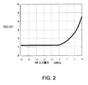
ET電源8は、供給制御信号18に従って供給電圧VCCのレベルを制御する。ET電源8の例は線形レギュレータ、スイッチング電源、ならびにリニアレギュレータおよびスイッチング電源の両方を利用するハイブリッド電源を含む。図2を短く参照して、示されるのは、実施の形態に従う、PA3へのRF入力電力と(供給制御信号118に対応する)供給電圧VCCとの間の関係のグラフである。水平軸は、PAへのRF入力電力を表す。それはRF入力信号17の振幅に対応する。垂直軸は、PA3への供給電圧VCCを表す。供給電圧VCCは、RF入力電力が−5dBmより大きいとき、供給電圧VCCがRF入力電力を実質的に追跡するように、包絡線追跡態様で制御される。RF入力電力が−5dBm未満であるとき、供給電圧VCCが最小のレベルの1.2Vに実質的に一定に保持されて、PA3が適切にバイアスされたままになることが注目される。
The
図1を再び参照して、デカップラ22および特徴付けブロック102は、RF・PAシステムを特徴付けて特徴付けテーブル33を生成するためのフィードバック経路を形成する。デカップラ22はRF出力信号12の結合されたもの23をフィードバック受信部24に与える。フィードバック受信部24は、結合された出力信号23をダウンコンバートし、ダウンコンバートされた信号を復調し、公式振幅=sqrt(I2+Q2)を利用してその振幅を推定することにより、RF出力信号12の振幅を推定する。次いで、フィードバック受信部24はRF出力信号12の振幅を示す出力振幅信号42を生成する。
Referring back to FIG. 1,
特徴付けブロック102は出力振幅信号42、RX信号11および他の情報を受信し、これらの入力を用いて、RF・PAシステムの性能特性(たとえば利得、電力効率、歪み、受信バンドノイズ)を測定する。性能特性の例は特に、利得、電力効率、歪みおよび受信バンドノイズを含む。
The
性能特性は、RF・PAシステムの動作条件の異なるレベル(たとえば異なる次元または状態)に対して、多くの異なるRF入力レベルおよび供給電圧値にわたって測定される。次いで、特徴付けブロック102は、異なるRF入力レベル、供給電圧値、動作条件レベル、RF出力レベル、および測定されたRF・PAシステムの性能レベルの間の関係を記述する特徴付け情報を含む1つ以上の特徴付けテーブル33を生成する。特徴付けテーブル33は、不揮発性メモリなどのようなメモリに保存することが可能である。
Performance characteristics are measured over many different RF input levels and supply voltage values for different levels (eg, different dimensions or states) of the operating conditions of the RF PA system. The
下記のテーブルは特徴付けテーブルにおいて見出され得るエントリの例である。 The following table is an example of an entry that can be found in the characterization table.

表1における動作条件は温度および周波数を含む。表1における性能特性は利得および電力効率を含む。表1は特徴付けテーブル33のほんの僅かな部分を示す。実際には、特徴付けテーブル33は、RF入力振幅と供給電圧値と動作条件レベルと性能特性とRF出力振幅との異なる組合せを捕捉する1つ以上のテーブルにわたる何百またはそれより多い異なるエントリを有してもよい。一実施の形態では、特徴付けテーブル33は、所与の動作条件下でRF入力振幅とRF出力振幅に対する供給電圧値と性能特性とを関連付ける式を含んでもよい。式は、異なる動作条件、RF入力振幅および供給電圧についての変数からRF・PAシステムの性能特性を計算してもよい。 The operating conditions in Table 1 include temperature and frequency. The performance characteristics in Table 1 include gain and power efficiency. Table 1 shows only a small part of the characterization table 33. In practice, the characterization table 33 includes hundreds or more different entries across one or more tables that capture different combinations of RF input amplitude, supply voltage value, operating condition level, performance characteristics and RF output amplitude. You may have. In one embodiment, the characterization table 33 may include formulas that relate supply voltage values to RF input amplitude and RF output amplitude and performance characteristics under a given operating condition. The equation may calculate the performance characteristics of the RF PA system from variables for different operating conditions, RF input amplitude and supply voltage.
供給制御ブロック104は特徴付けテーブル33における特徴付け情報を用いて、RF・PAシステムの1つ以上の動作条件(たとえば温度、周波数、変調、インピーダンス不整合)の現在のレベルについて、電力効率と歪みを均衡させる、供給制御信号18に対する値を判断する。特徴付けテーブル33はRF・PAシステムの通常動作中にRF・PAシステムで局所的に生成されるので、それは、他の態様で考えられ得るよりも実際の動作条件に適合するよう電力効率と歪みをより正確に均衡させる態様で供給制御ブロック104が供給電圧VCCを制御することを可能にする。
The
一実施の形態では、遅延整列ブロック(図示せず)が、さらに、ET電源8に、または可変利得RFアップコンバータ2内において時間遅延を挿入して、供給電圧VCCとRF出力信号12の振幅との間の適切な時間同期を保証してもよい。
In one embodiment, a delay alignment block (not shown) further inserts a time delay into the
図3は、実施の形態に従う、図1からのRF・PAシステムの、より詳細な図を示す。供給制御ブロック104はルックアップテーブル(LUT)ビルダブロック302とLUTと供給電圧調整ブロック314とデジタル−アナログ変換器(DAC)とを含む。LUTはデジタル供給電圧値に対する振幅信号110の振幅レベルを参照する。たとえば、LUTは、1dB離間された−21dB〜+10dBmのRF入力電力レベルに対応して、供給電圧値に対して32のエントリを有してもよい。
FIG. 3 shows a more detailed view of the RF PA system from FIG. 1 according to an embodiment.
LUTにおける初期の供給電圧値は、典型的には工場で典型的な条件下で典型的な無線受信機装置上で典型的なPAの特徴付けを通して判断される。LUTは、公称条件下で、PAの期待される利得に基いて、期待されるRF出力12信号振幅のさまざまな値に対して適切な公称の供給電圧値のこの集合で事前設定されてもよい。
The initial supply voltage value in the LUT is typically determined through typical PA characterization on a typical radio receiver device under typical conditions at the factory. The LUT may be preset with this set of nominal supply voltage values appropriate for various values of the expected
LUTは供給電圧値312を出力し、それらは、供給電圧調整回路314によって、調整された供給電圧値316に調整される。電圧調整回路114の動作は、特徴付けブロック102を参照して以下により詳細に説明される。調整された供給電圧値316は、デジタル−アナログ変換器DACでアナログ供給制御信号18に変換される。供給制御信号18はET電源8を制御して、PA3に電力を供給するために具体的な供給電圧VCCレベルを出力する。
The LUT outputs supply voltage values 312 which are adjusted to the adjusted
無線受信機における実際の動作中、PA3は、数例を挙げると、PAプロセスおよび製造公差、電源回路ばらつき、環境要因、温度、動作周波数、変調フォーマットおよびアンテナ不整合などのような要因に依って、工場での典型的なPA3の動作中のそれらとは異なる特性を示すかもしれない。特性におけるこれらの予測不能の変動のため、デフォルトLUTエントリは、目標電力効率および歪みレベルでRF・PAシステムを動作することに対して十分に適していないかもしれない。これらの変動を担うため、特徴付けブロック102は、供給電圧VCCに対する小さな変化でシステムを摂動させることにより、RF・PAシステムの性能特性を測定しながらも、RF・PAシステムにおける過剰な歪みを引起さないように、RF・PAシステムを特徴付ける。このプロセスはRF入力信号17の異なる動作条件レベルおよび振幅に対して繰り返されて、特徴付けテーブル33を生成する。次いで、LUTビルダ302は特徴付けテーブル33を用いてLUTにおける値を変化させて改善する。
During actual operation in a wireless receiver, PA3 depends on factors such as PA process and manufacturing tolerances, power supply circuit variations, environmental factors, temperature, operating frequency, modulation format and antenna mismatch, to name a few. May show different characteristics than those during typical PA3 operation in the factory. Because of these unpredictable variations in characteristics, the default LUT entry may not be well suited for operating an RF • PA system at a target power efficiency and distortion level. To account for these variations, the
代替的に、供給電圧VCCを摂動させる代りに、他の実施の形態は、RF入力信号17に摂動を導入して、RF入力信号17を摂動させながら性能特性を測定してもよい。
Alternatively, instead of perturbing the supply voltage VCC, other embodiments may introduce perturbations to the
特徴付けブロック102はテーブル生成ブロック322と歪み推定部324と効率推定部326とノイズ推定部352を含む。特徴付けは、典型的には、RF・PAシステムが通常の送信動作でオフライン較正モードなしに動作している間に生じる。言いかえれば、特徴付けは、送信変調部10が遠隔装置に送信されるべき情報を含むベースバンド信号1を生成している間に生じる。ベースバンド信号1はRF入力信号17に変換され、RF出力信号12に増幅される。RF入力振幅はLUTに与えられ、それは初期のLUT値を用いて、供給電圧値312を出力する。同時に、テーブル生成ブロック322は、さらに、供給電圧VCCのために目標の調整レベル(たとえば増倍係数)を指定する電圧調整信号318を生成する。次いで、供給電圧調整回路314は、供給電圧値312を、供給制御信号18に変換される調整された供給電圧値316に調整する。
The
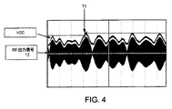
図4を短く参照して、実施の形態に従って、特徴付け中の供給電圧VCCに対する調整を示す波形が示される。図4は、RF出力信号12に対する波形と、RF出力信号12の振幅を追跡する供給電圧VCCに対する波形とを含む。時間T1に先立って、供給電圧VCCはデフォルト供給電圧値312を用いていかなる調整もなしに生成される。時間T1で、デフォルト供給電圧値312は電圧調整信号318によって調整され、それは供給電圧VCCにおいて不連続を引起す。不連続は、RF出力信号12におけるいかなる歪みも依然として規定上の振幅または位相誤り要件のしきい値より下に落ちるように、十分に小さい。時間T1の後、供給電圧VCCはデフォルトLUT値の調整により生成され続ける。その調整は時間T1の後に供給電圧VCCにおいて僅かな増大を引起す。他の実施の形態では、調整は、供給電圧VCCにおける増大の代りに、供給電圧VCCにおいて減少を引起す場合がある。
Referring briefly to FIG. 4, waveforms are shown illustrating adjustments to the supply voltage VCC being characterized, according to an embodiment. FIG. 4 includes a waveform for the
図3に戻って、効率推定部ブロック326は、調整された供給電圧VCCと関連付けられるPA3の電力効率を推定し、推定された電力効率を示す電力効率信号334を生成する。一実施の形態では、効率推定部40は、以下の式で電力効率を推定する:
P効率=(出力P×不整合)/消費P(式1)
P出力はPAの出力での電力である。P出力は、(出力振幅信号42によって示される)RF出力振幅の二乗により判断される。不整合は、PAの出力でのインピーダンス不整合を表す係数である。不整合は、PA3の出力に結合される順方向および逆方向接続される方向性結合器(図示せず)で検出される順方向電力と逆方向電力との間の電力比および位相差から計算されるインピーダンス不整合に基いて経験的に判断される固定値または可変値であってもよい。消費Pは、PA3によって消費される電力である。消費Pは、サンプリング回路340から得られたサンプリング信号332を通して、PA3に供給される電流および電圧をサンプリングし、次いで、サンプリングされた電流およびサンプリングされた電圧を乗算することによって判断される。他の実施の形態では、供給電圧VCCのレベルはどの所与の時間でも既知であるので、サンプリング回路340は供給電圧VCCの代りに供給電流のみをサンプリングする。
Returning to FIG. 3, the efficiency estimator block 326 estimates the power efficiency of the
P efficiency = (output P × mismatch) / consumption P (formula 1)
P output is the power at the output of the PA. The P output is determined by the square of the RF output amplitude (indicated by output amplitude signal 42). Mismatch is a coefficient representing impedance mismatch at the output of the PA. The mismatch is calculated from the power ratio and phase difference between forward and reverse power detected by a forward and reverse connected directional coupler (not shown) coupled to the output of PA3. It may be a fixed value or a variable value that is determined empirically based on the impedance mismatch that is made. Consumption P is the power consumed by PA3. The consumption P is determined by sampling the current and voltage supplied to PA3 through the sampling signal 332 obtained from the
歪み推定部ブロック324は、調整された供給電圧VCCと関連付けられるPA3の歪みを推定し、推定される歪みレベルを示す1つ以上の歪み信号336を生成する。一実施の形態では、歪み推定部ブロック324は、所望の送信情報を含むベースバンド信号1を受信する。歪み推定部ブロック324は、ベースバンド信号1の振幅を(出力振幅信号42によって示された)RF出力振幅と比較して、PA3の歪みを推定する。所望の送信信号とRF出力振幅との間のより大きな差は、より大きい量の歪みを示す。
The distortion estimator block 324 estimates the distortion of PA3 associated with the adjusted supply voltage VCC and generates one or more distortion signals 336 indicative of the estimated distortion level. In one embodiment, the distortion estimator block 324 receives a
他の実施の形態では、歪み推定部ブロック324は、RF出力振幅のサンプルを経時的に保存し、サンプルからPAのAM−AM歪み(つまり振幅歪み)またはAM−PM歪み(つまり位相歪み)を判断する。AM−AM歪みは供給電圧VCCにおける変化に対するRF出力振幅における変化の比として計算される。AM−PM歪みは供給電圧VCCにおける変化に対するRF出力位相における測定された変化の比として計算される。理想的には、AM−PM歪みおよびAM−PM歪みは平坦であるべきである。さらなる実施の形態では、歪み推定部ブロック324は隣接チャネル漏洩電力(ACP)の形式で歪みを測定することが可能である。 In other embodiments, the distortion estimator block 324 stores samples of RF output amplitude over time and derives PA AM-AM distortion (ie amplitude distortion) or AM-PM distortion (ie phase distortion) from the sample. to decide. AM-AM distortion is calculated as the ratio of the change in RF output amplitude to the change in supply voltage VCC. AM-PM distortion is calculated as the ratio of the measured change in RF output phase to the change in supply voltage VCC. Ideally, AM-PM distortion and AM-PM distortion should be flat. In a further embodiment, the distortion estimator block 324 may measure distortion in the form of adjacent channel leakage power (ACP).
いくつかの実施の形態では、歪みは、RF・PAシステムの記憶効果となって現れる多項式で表すことが可能である。記憶効果は、PAシステムにおける過去の状態はRF・PAシステムにおける現在の歪みのレベルに影響し得るという事実を指す。 In some embodiments, the distortion can be represented by a polynomial that appears as a memory effect of the RF PA system. The memory effect refers to the fact that past conditions in the PA system can affect the current level of distortion in the RF PA system.
ノイズ推定部ブロック352はRX信号11を受信し、RX信号11において受信バンドノイズ352を推定する。PA3に対する供給電圧VCC340を変化させることは、時にRX信号11にノイズを導入し得る。ノイズ推定部ブロックはこのノイズを推定し、次いで、受信バンドノイズ352のレベルを示すノイズ推定信号を生成する。
The noise
テーブル生成ブロック322は入力振幅信号110と出力振幅信号42と歪み信号336と電力効率信号326とノイズ推定信号353とを受信する。テーブル生成ブロック322は、特徴付けテーブル33に、RF入力振幅、調整された供給電圧VCCに対する供給電圧値、RF出力振幅、動作条件のレベル、および性能特性(たとえば利得、電力効率、歪み、ノイズ)のレベルを関連付けるエントリを生成する。このプロセスは、異なるRF入力振幅、異なる供給電圧値、および異なるレベルの動作条件に対して何度も繰り返されて、多くの異なるテーブルエントリを生成してもよい。結果は、たとえば、表1に示されるように、RF入力振幅と供給電圧値とRF出力振幅と動作条件と性能特性との間の関係について記述する特徴付け情報の集まりである。
The
一実施の形態では、テーブル生成ブロック322は、入力振幅信号110および出力振幅信号42からPA3の利得を推定する。他の実施の形態では、テーブル生成ブロック322は、RF入力信号に関して直接LUTから振幅情報を得て、この振幅情報を用いて利得を推定してもよい。
In one embodiment, the
一旦特徴付けテーブル33が作成されると、LUTビルダ302は特徴付けテーブル33を利用して、システムに現在ある現在の動作条件(たとえば温度、周波数、変調、不整合)に従ってLUTに対する供給電圧値312の新たな集合を生成する。たとえば、LUTビルダ302は、現在の動作条件が25℃の温度と1700MHzの搬送周波数とPSKの変調タイプと0のインピーダンス不整合とであることを示す信号を受信してもよい。次いで、LUTビルダ302は、この現在の動作条件の集合に対する供給電圧値312を生成する。いくつかの実施の形態では、LUTビルダブロック302は、LUTに対する入力として1つ以上の動作条件を用いる、より複雑なLUTを生成してもよい。
Once the characterization table 33 is created, the
供給電圧値312は、特徴付けテーブル33における情報から内挿または外挿されてもよい。代替的に、特徴付けテーブル33における式を利用して、LUTに対する新たな供給電圧値312を生成してもよい。 Supply voltage value 312 may be interpolated or extrapolated from information in characterization table 33. Alternatively, the formula in characterization table 33 may be used to generate a new supply voltage value 312 for the LUT.
一実施の形態では、LUTビルダ302は、RF・PAシステムに現在の動作条件下である範囲の目標性能レベルを動作させておくLUTを生成する。たとえば、PA3が、受入可能な目標範囲内において歪みを生じさせ、さらに、電力効率を受入可能な目標範囲内に有するように、LUTを生成することが可能である。LUTビルダ302は、さらに、具体的な目標性能レベルでRF・PAシステムを動作させておくLUTを生成してもよい。たとえば、PA3が一定の利得を有するように、LUTを生成することが可能である。他の例として、PA3が一定のAM−AM歪みを有するように、LUTを生成することが可能である。
In one embodiment, the
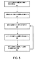
図5は、実施の形態に従う、RF・PAシステムにおける動作の方法を示す。ステップ502で、LUTは初期の供給電圧値312の集合で事前設定される。初期値は、典型的な動作条件下で典型的な無線受信機装置に対して適切な、典型的に包括的な値である。ステップ504で、RF・PAシステムは、アンテナ4を通して遠隔装置に送信される所望の送信情報とともにベースバンド信号1を生成することにより、通常の送信動作で動作する。RF・PAシステムは、さらに、供給電圧VCCの制御において、初期の供給電圧値312の集合を用いる。
FIG. 5 illustrates a method of operation in an RF PA system, according to an embodiment. At
ステップ506で、初期期間中、RF・PAシステムが通常の送信動作で動作している間に、特徴付けブロック102は、RF・PAシステムの動作を中断せずに、RF・PAシステムを特徴付ける。特徴付けブロック102は供給電圧VCCを調整するために供給電圧値312を調整する。特徴付けブロック102は、調整された供給電圧VCCと関連付けられる、結果として得られる性能(たとえば電力効率、歪み、および受信バンドノイズ)を評価する。次いで、特徴付けブロック102は、特徴付けテーブル33に対して新たなエントリを生成する。
At
ステップ508で、一旦特徴付けが完了すると、供給制御ブロック104は特徴付けテーブル33を用いて、LUTに対する新たな供給電圧値312を生成する。ステップ510で、後の期間中に、次いで、LUTに対する新たな供給電圧値312を用いて、供給電圧制御信号18およびしたがってさらに供給電圧VCCを制御する。ステップ506と508と510とを周期的な間隔で繰り返して、経時的に生じるかもしれないRF・PAシステムの特性におけるいかなる変化も捕捉し、さらにLUTを改善してもよい。
In
図6は、他の実施の形態に従う、特徴付け中の供給電圧VCCに対する調整を示す。図6は、供給電圧VCCとRF入力信号17の振幅とPA3への供給電流に対する波形を含む。ベースバンド信号1は無作為化された(つまり、無作為または擬似乱数的な)パターンで生成され、それは、RF入力信号17の振幅にも、同じランダム化されたパターンを持たせる。ベースバンド信号1の無作為化されたパターンは、RF入力信号17の振幅を、固定された振幅を有するリセット位置と無作為の振幅を有する無作為化された位置との間で交互させる。供給電圧VCCは異なる無作為化されたパターンを有する。供給電圧VCCの無作為化されたパターンも、固定された電圧レベルを有するリセット位置と無作為の電圧レベルを有する無作為化された位置との間で交互する。RF入力信号17の各新たな振幅は、供給電圧VCCの異なるレベルに対応する。無作為化されたパターンは特徴付けテーブル33の構築を促進し、専用オフライン特徴付けモードで生成されてもよい。先のように、特徴付けブロック102は、異なるRF入力振幅および供給電圧VCCレベルに対して電力効率および歪みレベルを推定して、特徴付けテーブル33に対する新たなエントリを生成する。
FIG. 6 shows an adjustment to the supply voltage VCC during characterization according to another embodiment. FIG. 6 includes waveforms for supply voltage VCC,
この開示を読むと同時に、当業者は、この開示に従って、RF・PAシステムのためのさらにさらなる代替的な構造的および機能上の設計を理解する。このように、この開示の特定の実施の形態および適用例が示され記述されたが、実施の形態は、ここに開示される構築物および構成要素そのものに制限されず、当業者に明らかな、さまざまな修正、変更および変形が、開示の精神および範囲から逸脱せずに、この開示の方法および装置の構成、動作および詳細において行われてもよいことが理解される。 Upon reading this disclosure, those skilled in the art will understand still further alternative structural and functional designs for the RF PA system in accordance with this disclosure. Thus, although specific embodiments and applications of this disclosure have been shown and described, the embodiments are not limited to the constructs and components themselves disclosed herein, and are apparent to those skilled in the art. It will be understood that various modifications, changes and variations may be made in the arrangement, operation and details of the methods and apparatus of this disclosure without departing from the spirit and scope of the disclosure.
Claims (18)
RF入力信号からRF出力信号を生成する電力増幅器を含み、前記電力増幅器は供給電圧によって電力を供給され;前記システムはさらに、
第1の期間に前記供給電圧を調整するための調整信号を生成して、前記第1の期間中に前記供給電圧を調整しながら特徴付け情報を生成する特徴付けブロックとを備え、前記特徴付け情報は、前記RF電力増幅器システムの1つ以上の動作条件の複数のレベルについての前記供給電圧と前記RF電力増幅器システム性能との間の関係に対応し、さらに;
前記RF入力信号の振幅を推定する振幅推定部ブロックと;
前記第1の期間中に、ルックアップテーブルにおける初期の供給電圧値および前記RF入力信号の振幅に基いて、前記電力増幅器への供給電圧を制御するための供給電圧制御信号を生成するとともに、第2の期間中に、前記特徴付け情報および前記RF入力信号の前記振幅に基いて、前記供給電圧制御信号を生成する供給制御ブロックとを含む、RF電力増幅器システム。 A radio frequency (RF) power amplifier system comprising:
A power amplifier that generates an RF output signal from an RF input signal, the power amplifier being powered by a supply voltage;
And it generates an adjustment signal for adjusting the supply voltage to the first period, and a characterization block to generate the characterization information while adjusting the supply voltage during the first period, the characterization The information corresponds to a relationship between the supply voltage and the RF power amplifier system performance for a plurality of levels of one or more operating conditions of the RF power amplifier system;
An amplitude estimation block for estimating the amplitude of the RF input signal;
During the first period, based on the amplitude of the initial supply voltage value and the RF input signal in the look-up table, and generates a supply voltage control signal for controlling the supply voltage to the power amplifier, the And a supply control block that generates the supply voltage control signal based on the characterization information and the amplitude of the RF input signal during two periods.
前記特徴付けブロックは、前記RF出力信号の振幅に基いて前記特徴付け情報を生成するように構成される、請求項1に記載のRF電力増幅器システム。 A feedback block for estimating an amplitude of the RF output signal;
The RF power amplifier system of claim 1, wherein the characterization block is configured to generate the characterization information based on an amplitude of the RF output signal.
電力増幅器によって、RF入力信号に基づいてRF出力信号を生成することと;
第1の期間中に、前記電力増幅器への供給電圧を調整するための調整信号を生成することと;
前記第1の期間において前記供給電圧を調整しながら特徴付け情報を生成することとを含み、前記特徴付け情報は、前記RF電力増幅器システムの動作条件の複数のレベルに対して、前記電力増幅器への前記供給電圧と前記電力増幅器の性能との間の関係に対応し、前記方法はさらに;
前記RF入力信号の振幅を推定することと;
前記第1の期間中に、ルックアップテーブルにおける初期の供給電圧値および前記RF入力信号の振幅に基いて、前記電力増幅器への前記供給電圧を制御するために供給電圧制御信号を生成することと;
第2の期間中に、前記特徴付け情報および前記RF入力信号の振幅に基いて、前記電力増幅器への前記供給電圧を制御するための前記供給電圧制御信号を生成することとを含む、方法。 A method of operation in a radio frequency (RF) power amplifier system comprising:
Generating an RF output signal based on the RF input signal by a power amplifier;
Generating an adjustment signal for adjusting a supply voltage to the power amplifier during a first period;
And a generating an adjustment while characterization information the supply voltage in the first period, the characterization information to a plurality of levels of operating conditions of the RF power amplifier system, to the power amplifier Corresponding to the relationship between the supply voltage and the performance of the power amplifier, the method further comprising:
Estimating the amplitude of the RF input signal;
During the first period, and it is based on the amplitude of the initial supply voltage value and the RF input signal in the look-up table, for generating a supply voltage control signal for controlling the supply voltage to the power amplifier ;
During the second period, based on the amplitude of the characterization information and the RF input signal, and generating the supply voltage control signal for controlling the supply voltage to the power amplifier, the method.
前記特徴付け情報は前記RF出力信号の振幅に基いて生成される、請求項13に記載の方法。 Further comprising estimating an amplitude of the RF output signal;
The method of claim 13, wherein the characterization information is generated based on an amplitude of the RF output signal.
前記特徴付け情報は前記RF電力増幅器システムの推定された性能に基いて生成される、請求項13に記載の方法。 Further comprising estimating the performance of the RF power amplifier system over multiple levels of the supply voltage;
The method of claim 13, wherein the characterization information is generated based on an estimated performance of the RF power amplifier system.
前記特徴付け情報に基いて、前記ルックアップテーブルを生成することと;
前記RF入力信号の振幅に対応する前記ルックアップテーブルにおける値に基いて、前記供給電圧制御信号を生成することとを含む、請求項13に記載の方法。 Generating the supply voltage control signal is:
Generating the lookup table based on the characterization information;
14. The method of claim 13 , comprising generating the supply voltage control signal based on a value in the look-up table corresponding to an amplitude of the RF input signal.
Applications Claiming Priority (3)
| Application Number | Priority Date | Filing Date | Title |
|---|---|---|---|
| US201361800350P | 2013-03-15 | 2013-03-15 | |
| US61/800,350 | 2013-03-15 | ||
| PCT/US2014/026431 WO2014151777A1 (en) | 2013-03-15 | 2014-03-13 | Envelope tracking system with internal power amplifier characterization |
Publications (3)
| Publication Number | Publication Date |
|---|---|
| JP2016512414A JP2016512414A (en) | 2016-04-25 |
| JP2016512414A5 JP2016512414A5 (en) | 2016-12-01 |
| JP6166457B2 true JP6166457B2 (en) | 2017-07-19 |
Family
ID=51524897
Family Applications (1)
| Application Number | Title | Priority Date | Filing Date |
|---|---|---|---|
| JP2016502142A Active JP6166457B2 (en) | 2013-03-15 | 2014-03-13 | Envelope tracking system with internal power amplifier characterization |
Country Status (8)
| Country | Link |
|---|---|
| US (2) | US9270239B2 (en) |
| EP (1) | EP2974006B1 (en) |
| JP (1) | JP6166457B2 (en) |
| KR (1) | KR102174242B1 (en) |
| CN (1) | CN105103443B (en) |
| HK (1) | HK1213372A1 (en) |
| TW (1) | TWI540829B (en) |
| WO (1) | WO2014151777A1 (en) |
Families Citing this family (56)
| Publication number | Priority date | Publication date | Assignee | Title |
|---|---|---|---|---|
| US8718579B2 (en) | 2012-03-04 | 2014-05-06 | Quantance, Inc. | Envelope tracking power amplifier system with delay calibration |
| US9042848B2 (en) * | 2012-12-19 | 2015-05-26 | Mediatek Singapore Pte. Ltd. | Method and apparatus for calibrating an envelope tracking system |
| CN105027429B (en) | 2013-03-14 | 2018-03-30 | 匡坦斯公司 | Envelope-tracking system with noise adjustment |
| EP2974006B1 (en) | 2013-03-15 | 2017-10-25 | Quantance, Inc. | Envelope tracking system with internal power amplifier characterization |
| US9231627B2 (en) * | 2013-11-06 | 2016-01-05 | Stmicroelectronics International N.V. | Adaptive ISO-Gain pre-distortion for an RF power amplifier operating in envelope tracking |
| DE102014105909A1 (en) * | 2014-04-28 | 2015-10-29 | Phoenix Contact Gmbh & Co. Kg | Power supply unit |
| US10333474B2 (en) * | 2014-05-19 | 2019-06-25 | Skyworks Solutions, Inc. | RF transceiver front end module with improved linearity |
| US9998241B2 (en) * | 2015-02-19 | 2018-06-12 | Mediatek Inc. | Envelope tracking (ET) closed-loop on-the-fly calibration |
| DE102015110238A1 (en) | 2015-06-25 | 2016-12-29 | Intel IP Corporation | A circuit and method for generating a radio frequency signal |
| WO2017019803A1 (en) * | 2015-07-28 | 2017-02-02 | Skyworks Solutions, Inc. | Power amplification system with programmable load line |
| US11201595B2 (en) * | 2015-11-24 | 2021-12-14 | Skyworks Solutions, Inc. | Cascode power amplifier with switchable output matching network |
| KR102594658B1 (en) * | 2016-12-23 | 2023-10-26 | 삼성전자주식회사 | Apparatus and method for controlling wireless transmission |
| US10181826B2 (en) | 2017-04-25 | 2019-01-15 | Qorvo Us, Inc. | Envelope tracking amplifier circuit |
| US10158330B1 (en) | 2017-07-17 | 2018-12-18 | Qorvo Us, Inc. | Multi-mode envelope tracking amplifier circuit |
| US10284412B2 (en) | 2017-07-17 | 2019-05-07 | Qorvo Us, Inc. | Voltage memory digital pre-distortion circuit |
| CN109286375B (en) * | 2017-07-19 | 2021-03-02 | 陕西亚成微电子股份有限公司 | Power supply for envelope tracking |
| US10326490B2 (en) | 2017-08-31 | 2019-06-18 | Qorvo Us, Inc. | Multi radio access technology power management circuit |
| US10530305B2 (en) | 2017-10-06 | 2020-01-07 | Qorvo Us, Inc. | Nonlinear bandwidth compression circuitry |
| US10439557B2 (en) | 2018-01-15 | 2019-10-08 | Qorvo Us, Inc. | Envelope tracking power management circuit |
| US10637408B2 (en) | 2018-01-18 | 2020-04-28 | Qorvo Us, Inc. | Envelope tracking voltage tracker circuit and related power management circuit |
| US10742170B2 (en) | 2018-02-01 | 2020-08-11 | Qorvo Us, Inc. | Envelope tracking circuit and related power amplifier system |
| US10944365B2 (en) | 2018-06-28 | 2021-03-09 | Qorvo Us, Inc. | Envelope tracking amplifier circuit |
| US11088618B2 (en) | 2018-09-05 | 2021-08-10 | Qorvo Us, Inc. | PWM DC-DC converter with linear voltage regulator for DC assist |
| US10911001B2 (en) | 2018-10-02 | 2021-02-02 | Qorvo Us, Inc. | Envelope tracking amplifier circuit |
| KR102226814B1 (en) * | 2018-10-26 | 2021-03-11 | 삼성전자 주식회사 | Apparatus and method for selectively supplying voltage to a plurality of amplifiers using switching regulator |
| US10985702B2 (en) | 2018-10-31 | 2021-04-20 | Qorvo Us, Inc. | Envelope tracking system |
| US11018638B2 (en) | 2018-10-31 | 2021-05-25 | Qorvo Us, Inc. | Multimode envelope tracking circuit and related apparatus |
| US10938351B2 (en) | 2018-10-31 | 2021-03-02 | Qorvo Us, Inc. | Envelope tracking system |
| US10680556B2 (en) | 2018-11-05 | 2020-06-09 | Qorvo Us, Inc. | Radio frequency front-end circuit |
| US11031909B2 (en) | 2018-12-04 | 2021-06-08 | Qorvo Us, Inc. | Group delay optimization circuit and related apparatus |
| US11082007B2 (en) | 2018-12-19 | 2021-08-03 | Qorvo Us, Inc. | Envelope tracking integrated circuit and related apparatus |
| JP2020107970A (en) * | 2018-12-26 | 2020-07-09 | 株式会社村田製作所 | Power circuit |
| US11146213B2 (en) | 2019-01-15 | 2021-10-12 | Qorvo Us, Inc. | Multi-radio access technology envelope tracking amplifier apparatus |
| US11025458B2 (en) | 2019-02-07 | 2021-06-01 | Qorvo Us, Inc. | Adaptive frequency equalizer for wide modulation bandwidth envelope tracking |
| US10998859B2 (en) | 2019-02-07 | 2021-05-04 | Qorvo Us, Inc. | Dual-input envelope tracking integrated circuit and related apparatus |
| US11233481B2 (en) | 2019-02-18 | 2022-01-25 | Qorvo Us, Inc. | Modulated power apparatus |
| US11374482B2 (en) | 2019-04-02 | 2022-06-28 | Qorvo Us, Inc. | Dual-modulation power management circuit |
| US11082009B2 (en) | 2019-04-12 | 2021-08-03 | Qorvo Us, Inc. | Envelope tracking power amplifier apparatus |
| US11018627B2 (en) | 2019-04-17 | 2021-05-25 | Qorvo Us, Inc. | Multi-bandwidth envelope tracking integrated circuit and related apparatus |
| US11424719B2 (en) | 2019-04-18 | 2022-08-23 | Qorvo Us, Inc. | Multi-bandwidth envelope tracking integrated circuit |
| US11031911B2 (en) | 2019-05-02 | 2021-06-08 | Qorvo Us, Inc. | Envelope tracking integrated circuit and related apparatus |
| US11349436B2 (en) | 2019-05-30 | 2022-05-31 | Qorvo Us, Inc. | Envelope tracking integrated circuit |
| US11539289B2 (en) | 2019-08-02 | 2022-12-27 | Qorvo Us, Inc. | Multi-level charge pump circuit |
| US11309922B2 (en) | 2019-12-13 | 2022-04-19 | Qorvo Us, Inc. | Multi-mode power management integrated circuit in a small formfactor wireless apparatus |
| US11349513B2 (en) | 2019-12-20 | 2022-05-31 | Qorvo Us, Inc. | Envelope tracking system |
| US11539330B2 (en) | 2020-01-17 | 2022-12-27 | Qorvo Us, Inc. | Envelope tracking integrated circuit supporting multiple types of power amplifiers |
| US11716057B2 (en) | 2020-01-28 | 2023-08-01 | Qorvo Us, Inc. | Envelope tracking circuitry |
| US11728774B2 (en) | 2020-02-26 | 2023-08-15 | Qorvo Us, Inc. | Average power tracking power management integrated circuit |
| JP2021153248A (en) * | 2020-03-24 | 2021-09-30 | 株式会社村田製作所 | Power amplifier evaluation method and measurement system |
| US11196392B2 (en) | 2020-03-30 | 2021-12-07 | Qorvo Us, Inc. | Device and device protection system |
| US11923812B2 (en) | 2020-08-12 | 2024-03-05 | Qorvo Us, Inc. | Delay-compensating power management integrated circuit |
| US11929712B2 (en) | 2020-08-12 | 2024-03-12 | Qorvo Us, Inc. | Delay-compensating power management circuit |
| US20220052651A1 (en) * | 2020-08-12 | 2022-02-17 | Qorvo Us, Inc. | Systems and methods for providing an envelope tracking power supply voltage |
| US11588449B2 (en) | 2020-09-25 | 2023-02-21 | Qorvo Us, Inc. | Envelope tracking power amplifier apparatus |
| US11728796B2 (en) | 2020-10-14 | 2023-08-15 | Qorvo Us, Inc. | Inverted group delay circuit |
| US11909385B2 (en) | 2020-10-19 | 2024-02-20 | Qorvo Us, Inc. | Fast-switching power management circuit and related apparatus |
Family Cites Families (53)
| Publication number | Priority date | Publication date | Assignee | Title |
|---|---|---|---|---|
| JPH0644716B2 (en) * | 1984-08-14 | 1994-06-08 | 日本電気株式会社 | Wireless communication device |
| US6084468A (en) | 1997-10-06 | 2000-07-04 | Motorola, Inc. | Method and apparatus for high efficiency wideband power amplification |
| US6130910A (en) | 1997-11-03 | 2000-10-10 | Motorola, Inc. | Method and apparatus for high efficiency wideband power amplification |
| US6356146B1 (en) | 1999-07-13 | 2002-03-12 | Pmc-Sierra, Inc. | Amplifier measurement and modeling processes for use in generating predistortion parameters |
| GB2370435A (en) | 2000-12-22 | 2002-06-26 | Nokia Mobile Phones Ltd | A polar loop transmitter for a mobile phone |
| AUPR438601A0 (en) | 2001-04-11 | 2001-05-17 | Cochlear Limited | Variable sensitivity control for a cochlear implant |
| US6683496B2 (en) * | 2001-08-20 | 2004-01-27 | Harris Corporation | System and method for minimizing dissipation in RF power amplifiers |
| US6784744B2 (en) | 2001-09-27 | 2004-08-31 | Powerq Technologies, Inc. | Amplifier circuits and methods |
| US7551688B2 (en) | 2002-04-18 | 2009-06-23 | Nokia Corporation | Waveforms for envelope tracking transmitter |
| US6646501B1 (en) * | 2002-06-25 | 2003-11-11 | Nortel Networks Limited | Power amplifier configuration |
| WO2004032345A1 (en) | 2002-10-03 | 2004-04-15 | Matsushita Electric Industrial Co., Ltd. | Transmitting method and transmitter apparatus |
| CN100581052C (en) * | 2004-08-13 | 2010-01-13 | 深圳赛意法微电子有限公司 | Automatic gain control system with self-adaptive climb and decay time |
| US7190221B2 (en) * | 2004-10-22 | 2007-03-13 | Nokia Corporation | Method and apparatus for maintaining constant linearity for a power amplifier over varying load conditions |
| US7348842B2 (en) | 2005-01-19 | 2008-03-25 | Micro-Mobio | Multi-substrate RF module for wireless communication devices |
| US20070066224A1 (en) * | 2005-02-28 | 2007-03-22 | Sirit, Inc. | High efficiency RF amplifier and envelope modulator |
| US20060199553A1 (en) | 2005-03-07 | 2006-09-07 | Andrew Corporation | Integrated transceiver with envelope tracking |
| US7418032B2 (en) | 2005-03-15 | 2008-08-26 | International Business Machines Corporation | Altering power consumption in communication links based on measured noise |
| WO2006114792A1 (en) | 2005-04-27 | 2006-11-02 | Paragon Communications Ltd. | Transformer-capacitor enhancement circuitry for power amplifiers |
| US7761066B2 (en) | 2006-01-27 | 2010-07-20 | Marvell World Trade Ltd. | Variable power adaptive transmitter |
| US8032097B2 (en) | 2006-02-03 | 2011-10-04 | Quantance, Inc. | Amplitude error de-glitching circuit and method of operating |
| US7522676B2 (en) | 2006-02-06 | 2009-04-21 | Nokia Corporation | Method and system for transmitter envelope delay calibration |
| JP2008283678A (en) | 2007-04-11 | 2008-11-20 | Panasonic Corp | Transmission circuit and communication device |
| US7466195B2 (en) | 2007-05-18 | 2008-12-16 | Quantance, Inc. | Error driven RF power amplifier control with increased efficiency |
| US20090004981A1 (en) * | 2007-06-27 | 2009-01-01 | Texas Instruments Incorporated | High efficiency digital transmitter incorporating switching power supply and linear power amplifier |
| US8463189B2 (en) * | 2007-07-31 | 2013-06-11 | Texas Instruments Incorporated | Predistortion calibration and built in self testing of a radio frequency power amplifier using subharmonic mixing |
| US7783269B2 (en) * | 2007-09-20 | 2010-08-24 | Quantance, Inc. | Power amplifier controller with polar transmitter |
| US8014735B2 (en) * | 2007-11-06 | 2011-09-06 | Quantance, Inc. | RF power amplifier controlled by estimated distortion level of output signal of power amplifier |
| GB0725110D0 (en) | 2007-12-21 | 2008-01-30 | Wolfson Microelectronics Plc | Gain control based on noise level |
| US8620233B2 (en) | 2008-04-11 | 2013-12-31 | Samsung Electroncs Co., Ltd. | Method of power amplifier predistortion adaptation using compression detection |
| US8072205B1 (en) | 2008-04-29 | 2011-12-06 | Analog Devices, Inc. | Peak-to-average measurement with envelope pre-detection |
| US7782134B2 (en) * | 2008-09-09 | 2010-08-24 | Quantance, Inc. | RF power amplifier system with impedance modulation |
| US8018277B2 (en) * | 2008-09-09 | 2011-09-13 | Quantance, Inc. | RF power amplifier system with impedance modulation |
| US8331883B2 (en) * | 2008-10-30 | 2012-12-11 | Apple Inc. | Electronic devices with calibrated radio frequency communications circuitry |
| US8064852B2 (en) * | 2008-11-13 | 2011-11-22 | Panasonic Corporation | Methods and apparatus for dynamically compensating for DC offset drift and other PVT-related signal variations in polar transmitters |
| WO2010064091A1 (en) | 2008-12-03 | 2010-06-10 | Freescale Semiconductor, Inc. | Operating parameter control for a power amplifier |
| US8744009B2 (en) | 2009-09-25 | 2014-06-03 | General Dynamics C4 Systems, Inc. | Reducing transmitter-to-receiver non-linear distortion at a transmitter prior to estimating and cancelling known non-linear distortion at a receiver |
| US8731496B2 (en) * | 2009-12-18 | 2014-05-20 | Quantance, Inc. | Power amplifier power controller |
| US8183917B2 (en) * | 2010-06-04 | 2012-05-22 | Quantance, Inc. | RF power amplifier circuit with mismatch tolerance |
| EP2673881B1 (en) | 2011-02-07 | 2019-02-06 | Skyworks Solutions, Inc. | Apparatus and methods for envelope tracking calibration |
| GB2489002A (en) | 2011-03-14 | 2012-09-19 | Nujira Ltd | Delay adjustment to reduce distortion in an envelope tracking transmitter |
| GB2489497A (en) * | 2011-03-31 | 2012-10-03 | Nujira Ltd | Matching the properties of the envelope path to the properties of the main signal path in an envelope tracking amplifier |
| US8718188B2 (en) | 2011-04-25 | 2014-05-06 | Skyworks Solutions, Inc. | Apparatus and methods for envelope tracking |
| US9066368B2 (en) | 2011-06-08 | 2015-06-23 | Broadcom Corporation | Method of calibrating the delay of an envelope tracking signal |
| US9083453B2 (en) | 2011-06-23 | 2015-07-14 | Qualcomm Incorporated | Power supply generator with noise cancellation |
| US8754706B2 (en) | 2011-08-02 | 2014-06-17 | Qualcomm Incorporated | Power based feedback for improved power amplifier (PA) efficiency |
| US20130076418A1 (en) | 2011-09-27 | 2013-03-28 | Intel Mobile Communications GmbH | System and Method for Calibration of Timing Mismatch for Envelope Tracking Transmit Systems |
| US8880012B2 (en) | 2012-01-19 | 2014-11-04 | Motorola Mobility Llc | Method and apparatus for resource block based transmitter optimization in wireless communication devices |
| JP5624569B2 (en) * | 2012-02-17 | 2014-11-12 | 株式会社東芝 | Power amplifier |
| US8718579B2 (en) * | 2012-03-04 | 2014-05-06 | Quantance, Inc. | Envelope tracking power amplifier system with delay calibration |
| US20140241462A1 (en) | 2013-02-26 | 2014-08-28 | Nvidia Corporation | Circuit and method for envelope tracking and envelope-tracking transmitter for radio-frequency transmission |
| CN105027429B (en) | 2013-03-14 | 2018-03-30 | 匡坦斯公司 | Envelope-tracking system with noise adjustment |
| EP2974006B1 (en) | 2013-03-15 | 2017-10-25 | Quantance, Inc. | Envelope tracking system with internal power amplifier characterization |
| GB2519361B (en) | 2013-10-21 | 2015-09-16 | Nujira Ltd | Reduced bandwidth of signal in an envelope path for envelope tracking system |
-
2014
- 2014-03-13 EP EP14767467.5A patent/EP2974006B1/en active Active
- 2014-03-13 JP JP2016502142A patent/JP6166457B2/en active Active
- 2014-03-13 WO PCT/US2014/026431 patent/WO2014151777A1/en active Application Filing
- 2014-03-13 KR KR1020157024837A patent/KR102174242B1/en active IP Right Grant
- 2014-03-13 US US14/208,528 patent/US9270239B2/en active Active
- 2014-03-13 CN CN201480011165.7A patent/CN105103443B/en active Active
- 2014-03-14 TW TW103109774A patent/TWI540829B/en active
-
2016
- 2016-02-04 US US15/015,195 patent/US9762184B2/en active Active
- 2016-02-05 HK HK16101368.4A patent/HK1213372A1/en unknown
Also Published As
| Publication number | Publication date |
|---|---|
| US20160156316A1 (en) | 2016-06-02 |
| HK1213372A1 (en) | 2016-06-30 |
| KR102174242B1 (en) | 2020-11-04 |
| EP2974006A1 (en) | 2016-01-20 |
| KR20150129731A (en) | 2015-11-20 |
| EP2974006A4 (en) | 2016-07-13 |
| US9270239B2 (en) | 2016-02-23 |
| WO2014151777A1 (en) | 2014-09-25 |
| CN105103443B (en) | 2018-01-02 |
| US20140266423A1 (en) | 2014-09-18 |
| CN105103443A (en) | 2015-11-25 |
| US9762184B2 (en) | 2017-09-12 |
| EP2974006B1 (en) | 2017-10-25 |
| TW201445874A (en) | 2014-12-01 |
| JP2016512414A (en) | 2016-04-25 |
| TWI540829B (en) | 2016-07-01 |
Similar Documents
| Publication | Publication Date | Title |
|---|---|---|
| JP6166457B2 (en) | Envelope tracking system with internal power amplifier characterization | |
| JP6247787B1 (en) | ET system with noise adjustment | |
| CN107093987B (en) | Envelope tracking system and related mobile communication device and storage medium | |
| EP3032737B1 (en) | Envelope tracking path delay fine tuning and calibration | |
| US9998241B2 (en) | Envelope tracking (ET) closed-loop on-the-fly calibration | |
| EP2766989B1 (en) | Apparatus and method for calibration of supply modulation in transmitter | |
| US9042848B2 (en) | Method and apparatus for calibrating an envelope tracking system | |
| US8014735B2 (en) | RF power amplifier controlled by estimated distortion level of output signal of power amplifier | |
| US9118366B2 (en) | Method and apparatus for calibrating an envelope tracking system | |
| CN104300915A (en) | Systems and methods utilizing adaptive envelope tracking | |
| KR101618429B1 (en) | Envelope tracking system and method for calibrating a supply voltage of an envelope tracking power amplifier | |
| US7983359B2 (en) | Synchronization techniques for polar transmitters | |
| US9668208B2 (en) | Operating point setting of an amplifier | |
| WO2013134025A1 (en) | Noise optimized envelope tracking system for power amplifiers | |
| JP2009194575A (en) | Transmission device | |
| JP2013005353A (en) | Power amplifier and power amplification method | |
| US8742865B2 (en) | Polar modulation transmission circuit and polar modulation transmission method | |
| CN117941248A (en) | Transmission setting selection |
Legal Events
| Date | Code | Title | Description |
|---|---|---|---|
| A521 | Request for written amendment filed |
Free format text: JAPANESE INTERMEDIATE CODE: A523 Effective date: 20161012 |
|
| A621 | Written request for application examination |
Free format text: JAPANESE INTERMEDIATE CODE: A621 Effective date: 20161012 |
|
| A871 | Explanation of circumstances concerning accelerated examination |
Free format text: JAPANESE INTERMEDIATE CODE: A871 Effective date: 20161012 |
|
| A975 | Report on accelerated examination |
Free format text: JAPANESE INTERMEDIATE CODE: A971005 Effective date: 20161227 |
|
| A131 | Notification of reasons for refusal |
Free format text: JAPANESE INTERMEDIATE CODE: A131 Effective date: 20170124 |
|
| A521 | Request for written amendment filed |
Free format text: JAPANESE INTERMEDIATE CODE: A523 Effective date: 20170217 |
|
| TRDD | Decision of grant or rejection written | ||
| A01 | Written decision to grant a patent or to grant a registration (utility model) |
Free format text: JAPANESE INTERMEDIATE CODE: A01 Effective date: 20170523 |
|
| A61 | First payment of annual fees (during grant procedure) |
Free format text: JAPANESE INTERMEDIATE CODE: A61 Effective date: 20170622 |
|
| R150 | Certificate of patent or registration of utility model |
Ref document number: 6166457 Country of ref document: JP Free format text: JAPANESE INTERMEDIATE CODE: R150 |
|
| R250 | Receipt of annual fees |
Free format text: JAPANESE INTERMEDIATE CODE: R250 |
|
| R250 | Receipt of annual fees |
Free format text: JAPANESE INTERMEDIATE CODE: R250 |
|
| R250 | Receipt of annual fees |
Free format text: JAPANESE INTERMEDIATE CODE: R250 |
|
| R250 | Receipt of annual fees |
Free format text: JAPANESE INTERMEDIATE CODE: R250 |