JP2016513077A - Triangulene oligomers and polymers and their use as hole conducting materials - Google Patents
Triangulene oligomers and polymers and their use as hole conducting materials Download PDFInfo
- Publication number
- JP2016513077A JP2016513077A JP2015553056A JP2015553056A JP2016513077A JP 2016513077 A JP2016513077 A JP 2016513077A JP 2015553056 A JP2015553056 A JP 2015553056A JP 2015553056 A JP2015553056 A JP 2015553056A JP 2016513077 A JP2016513077 A JP 2016513077A
- Authority
- JP
- Japan
- Prior art keywords
- amino
- compound
- formula
- unsubstituted
- aryl
- Prior art date
- Legal status (The legal status is an assumption and is not a legal conclusion. Google has not performed a legal analysis and makes no representation as to the accuracy of the status listed.)
- Withdrawn
Links
- YEBBJLDJFJIOFO-UHFFFAOYSA-N hexacyclo[11.7.1.13,19.02,7.09,21.015,20]docosa-1,3,5,7,9(21),10,12,15,17,19-decaene Chemical compound C1=CC=C2CC3=C4C(CC5=CC=CC6=CC1=C2C4=C56)=CC=C3 YEBBJLDJFJIOFO-UHFFFAOYSA-N 0.000 title abstract description 25
- 229920000642 polymer Polymers 0.000 title abstract description 20
- 229930183637 triangulene Natural products 0.000 title abstract description 15
- 239000004020 conductor Substances 0.000 title description 20
- -1 Hydroxy, mercapto, nitro, cyanato, thiocyanato, formyl Chemical group 0.000 claims description 755
- 239000004065 semiconductor Substances 0.000 claims description 117
- 150000001875 compounds Chemical class 0.000 claims description 109
- 150000004706 metal oxides Chemical class 0.000 claims description 90
- 229910044991 metal oxide Inorganic materials 0.000 claims description 89
- 125000002924 primary amino group Chemical group [H]N([H])* 0.000 claims description 80
- 238000000034 method Methods 0.000 claims description 79
- 238000006243 chemical reaction Methods 0.000 claims description 68
- 125000003118 aryl group Chemical group 0.000 claims description 59
- 239000000758 substrate Substances 0.000 claims description 55
- 239000000463 material Substances 0.000 claims description 54
- 125000000753 cycloalkyl group Chemical group 0.000 claims description 50
- 239000000203 mixture Substances 0.000 claims description 47
- 125000000592 heterocycloalkyl group Chemical group 0.000 claims description 43
- 125000001072 heteroaryl group Chemical group 0.000 claims description 42
- 229910052739 hydrogen Inorganic materials 0.000 claims description 41
- 239000001257 hydrogen Substances 0.000 claims description 41
- 125000000217 alkyl group Chemical group 0.000 claims description 40
- 125000000547 substituted alkyl group Chemical group 0.000 claims description 25
- 125000003545 alkoxy group Chemical group 0.000 claims description 24
- 125000004414 alkyl thio group Chemical group 0.000 claims description 21
- 229910052794 bromium Inorganic materials 0.000 claims description 21
- 229910052801 chlorine Inorganic materials 0.000 claims description 21
- 229910052731 fluorine Inorganic materials 0.000 claims description 21
- 238000004519 manufacturing process Methods 0.000 claims description 21
- 230000005525 hole transport Effects 0.000 claims description 20
- 150000002431 hydrogen Chemical class 0.000 claims description 19
- UFHFLCQGNIYNRP-UHFFFAOYSA-N Hydrogen Chemical compound [H][H] UFHFLCQGNIYNRP-UHFFFAOYSA-N 0.000 claims description 18
- 125000004104 aryloxy group Chemical group 0.000 claims description 18
- 230000005669 field effect Effects 0.000 claims description 18
- 125000005110 aryl thio group Chemical group 0.000 claims description 14
- 239000003054 catalyst Substances 0.000 claims description 13
- 125000000000 cycloalkoxy group Chemical group 0.000 claims description 12
- 229910052740 iodine Inorganic materials 0.000 claims description 12
- XEEYBQQBJWHFJM-UHFFFAOYSA-N Iron Chemical compound [Fe] XEEYBQQBJWHFJM-UHFFFAOYSA-N 0.000 claims description 11
- 125000002252 acyl group Chemical group 0.000 claims description 11
- 125000003917 carbamoyl group Chemical group [H]N([H])C(*)=O 0.000 claims description 11
- 239000011358 absorbing material Substances 0.000 claims description 10
- 125000005196 alkyl carbonyloxy group Chemical group 0.000 claims description 10
- 125000003739 carbamimidoyl group Chemical group C(N)(=N)* 0.000 claims description 10
- 229910052796 boron Inorganic materials 0.000 claims description 9
- 125000005366 cycloalkylthio group Chemical group 0.000 claims description 9
- YCWSUKQGVSGXJO-NTUHNPAUSA-N nifuroxazide Chemical group C1=CC(O)=CC=C1C(=O)N\N=C\C1=CC=C([N+]([O-])=O)O1 YCWSUKQGVSGXJO-NTUHNPAUSA-N 0.000 claims description 8
- 229910052723 transition metal Inorganic materials 0.000 claims description 7
- 150000003624 transition metals Chemical class 0.000 claims description 7
- 150000001602 bicycloalkyls Chemical group 0.000 claims description 6
- 125000000392 cycloalkenyl group Chemical group 0.000 claims description 6
- JRTIUDXYIUKIIE-KZUMESAESA-N (1z,5z)-cycloocta-1,5-diene;nickel Chemical compound [Ni].C\1C\C=C/CC\C=C/1.C\1C\C=C/CC\C=C/1 JRTIUDXYIUKIIE-KZUMESAESA-N 0.000 claims description 5
- 125000003342 alkenyl group Chemical group 0.000 claims description 5
- 125000000304 alkynyl group Chemical group 0.000 claims description 5
- 125000004435 hydrogen atom Chemical group [H]* 0.000 claims description 5
- 125000002496 methyl group Chemical group [H]C([H])([H])* 0.000 claims description 5
- MUBZPKHOEPUJKR-UHFFFAOYSA-N Oxalic acid Chemical compound OC(=O)C(O)=O MUBZPKHOEPUJKR-UHFFFAOYSA-N 0.000 claims description 4
- 125000004457 alkyl amino carbonyl group Chemical group 0.000 claims description 4
- 125000004390 alkyl sulfonyl group Chemical group 0.000 claims description 4
- 125000004391 aryl sulfonyl group Chemical group 0.000 claims description 4
- 238000004040 coloring Methods 0.000 claims description 4
- 125000004473 dialkylaminocarbonyl group Chemical group 0.000 claims description 4
- RMGVZKRVHHSUIM-UHFFFAOYSA-N dithionic acid Chemical compound OS(=O)(=O)S(O)(=O)=O RMGVZKRVHHSUIM-UHFFFAOYSA-N 0.000 claims description 4
- 125000005553 heteroaryloxy group Chemical group 0.000 claims description 4
- 239000010410 layer Substances 0.000 description 212
- 239000000975 dye Substances 0.000 description 68
- DZBUGLKDJFMEHC-UHFFFAOYSA-N acridine Chemical compound C1=CC=CC2=CC3=CC=CC=C3N=C21 DZBUGLKDJFMEHC-UHFFFAOYSA-N 0.000 description 56
- 239000000460 chlorine Substances 0.000 description 43
- 239000000243 solution Substances 0.000 description 29
- 229910052751 metal Inorganic materials 0.000 description 27
- 239000002184 metal Substances 0.000 description 27
- ZMXDDKWLCZADIW-UHFFFAOYSA-N N,N-Dimethylformamide Chemical compound CN(C)C=O ZMXDDKWLCZADIW-UHFFFAOYSA-N 0.000 description 25
- LFQSCWFLJHTTHZ-UHFFFAOYSA-N Ethanol Chemical compound CCO LFQSCWFLJHTTHZ-UHFFFAOYSA-N 0.000 description 24
- OKKJLVBELUTLKV-UHFFFAOYSA-N Methanol Chemical compound OC OKKJLVBELUTLKV-UHFFFAOYSA-N 0.000 description 24
- VYPSYNLAJGMNEJ-UHFFFAOYSA-N Silicium dioxide Chemical compound O=[Si]=O VYPSYNLAJGMNEJ-UHFFFAOYSA-N 0.000 description 23
- YXFVVABEGXRONW-UHFFFAOYSA-N Toluene Chemical compound CC1=CC=CC=C1 YXFVVABEGXRONW-UHFFFAOYSA-N 0.000 description 21
- VLKZOEOYAKHREP-UHFFFAOYSA-N n-Hexane Chemical compound CCCCCC VLKZOEOYAKHREP-UHFFFAOYSA-N 0.000 description 20
- 239000007787 solid Substances 0.000 description 20
- YMWUJEATGCHHMB-UHFFFAOYSA-N Dichloromethane Chemical compound ClCCl YMWUJEATGCHHMB-UHFFFAOYSA-N 0.000 description 19
- 229910010413 TiO 2 Inorganic materials 0.000 description 19
- XLOMVQKBTHCTTD-UHFFFAOYSA-N Zinc monoxide Chemical compound [Zn]=O XLOMVQKBTHCTTD-UHFFFAOYSA-N 0.000 description 18
- 239000011737 fluorine Substances 0.000 description 17
- 239000002904 solvent Substances 0.000 description 17
- YCKRFDGAMUMZLT-UHFFFAOYSA-N Fluorine atom Chemical compound [F] YCKRFDGAMUMZLT-UHFFFAOYSA-N 0.000 description 16
- 230000015572 biosynthetic process Effects 0.000 description 15
- XKRFYHLGVUSROY-UHFFFAOYSA-N Argon Chemical compound [Ar] XKRFYHLGVUSROY-UHFFFAOYSA-N 0.000 description 12
- BASFCYQUMIYNBI-UHFFFAOYSA-N platinum Chemical compound [Pt] BASFCYQUMIYNBI-UHFFFAOYSA-N 0.000 description 12
- 125000001424 substituent group Chemical group 0.000 description 12
- WKBOTKDWSSQWDR-UHFFFAOYSA-N Bromine atom Chemical compound [Br] WKBOTKDWSSQWDR-UHFFFAOYSA-N 0.000 description 11
- ZAMOUSCENKQFHK-UHFFFAOYSA-N Chlorine atom Chemical compound [Cl] ZAMOUSCENKQFHK-UHFFFAOYSA-N 0.000 description 11
- BQCADISMDOOEFD-UHFFFAOYSA-N Silver Chemical compound [Ag] BQCADISMDOOEFD-UHFFFAOYSA-N 0.000 description 11
- GDTBXPJZTBHREO-UHFFFAOYSA-N bromine Substances BrBr GDTBXPJZTBHREO-UHFFFAOYSA-N 0.000 description 11
- 238000004440 column chromatography Methods 0.000 description 11
- 239000011521 glass Substances 0.000 description 11
- 238000010438 heat treatment Methods 0.000 description 11
- PXHVJJICTQNCMI-UHFFFAOYSA-N nickel Substances [Ni] PXHVJJICTQNCMI-UHFFFAOYSA-N 0.000 description 11
- 239000002245 particle Substances 0.000 description 11
- 239000000377 silicon dioxide Substances 0.000 description 11
- 229910052709 silver Inorganic materials 0.000 description 11
- 239000004332 silver Substances 0.000 description 11
- 238000000576 coating method Methods 0.000 description 10
- 239000006185 dispersion Substances 0.000 description 10
- XOLBLPGZBRYERU-UHFFFAOYSA-N tin dioxide Chemical compound O=[Sn]=O XOLBLPGZBRYERU-UHFFFAOYSA-N 0.000 description 10
- 229910001887 tin oxide Inorganic materials 0.000 description 10
- 229910018072 Al 2 O 3 Inorganic materials 0.000 description 9
- XEKOWRVHYACXOJ-UHFFFAOYSA-N Ethyl acetate Chemical compound CCOC(C)=O XEKOWRVHYACXOJ-UHFFFAOYSA-N 0.000 description 9
- PCLIMKBDDGJMGD-UHFFFAOYSA-N N-bromosuccinimide Chemical compound BrN1C(=O)CCC1=O PCLIMKBDDGJMGD-UHFFFAOYSA-N 0.000 description 9
- LQZMLBORDGWNPD-UHFFFAOYSA-N N-iodosuccinimide Chemical compound IN1C(=O)CCC1=O LQZMLBORDGWNPD-UHFFFAOYSA-N 0.000 description 9
- GWEVSGVZZGPLCZ-UHFFFAOYSA-N Titan oxide Chemical compound O=[Ti]=O GWEVSGVZZGPLCZ-UHFFFAOYSA-N 0.000 description 9
- 125000003178 carboxy group Chemical group [H]OC(*)=O 0.000 description 9
- 125000004122 cyclic group Chemical group 0.000 description 9
- 238000000151 deposition Methods 0.000 description 9
- 238000005401 electroluminescence Methods 0.000 description 9
- 230000005281 excited state Effects 0.000 description 9
- 230000014509 gene expression Effects 0.000 description 9
- 150000003839 salts Chemical class 0.000 description 9
- 239000011787 zinc oxide Substances 0.000 description 9
- VEXZGXHMUGYJMC-UHFFFAOYSA-N Hydrochloric acid Chemical compound Cl VEXZGXHMUGYJMC-UHFFFAOYSA-N 0.000 description 8
- 238000010521 absorption reaction Methods 0.000 description 8
- 230000000903 blocking effect Effects 0.000 description 8
- 125000004432 carbon atom Chemical group C* 0.000 description 8
- 150000007942 carboxylates Chemical class 0.000 description 8
- 125000004093 cyano group Chemical group *C#N 0.000 description 8
- 239000010408 film Substances 0.000 description 8
- 230000006870 function Effects 0.000 description 8
- 239000007788 liquid Substances 0.000 description 8
- 125000001997 phenyl group Chemical group [H]C1=C([H])C([H])=C(*)C([H])=C1[H] 0.000 description 8
- BDHFUVZGWQCTTF-UHFFFAOYSA-M sulfonate Chemical compound [O-]S(=O)=O BDHFUVZGWQCTTF-UHFFFAOYSA-M 0.000 description 8
- 238000007740 vapor deposition Methods 0.000 description 8
- XDXWNHPWWKGTKO-UHFFFAOYSA-N 207739-72-8 Chemical compound C1=CC(OC)=CC=C1N(C=1C=C2C3(C4=CC(=CC=C4C2=CC=1)N(C=1C=CC(OC)=CC=1)C=1C=CC(OC)=CC=1)C1=CC(=CC=C1C1=CC=C(C=C13)N(C=1C=CC(OC)=CC=1)C=1C=CC(OC)=CC=1)N(C=1C=CC(OC)=CC=1)C=1C=CC(OC)=CC=1)C1=CC=C(OC)C=C1 XDXWNHPWWKGTKO-UHFFFAOYSA-N 0.000 description 7
- 229910052782 aluminium Inorganic materials 0.000 description 7
- XAGFODPZIPBFFR-UHFFFAOYSA-N aluminium Chemical compound [Al] XAGFODPZIPBFFR-UHFFFAOYSA-N 0.000 description 7
- 238000009792 diffusion process Methods 0.000 description 7
- 125000005842 heteroatom Chemical group 0.000 description 7
- 125000002887 hydroxy group Chemical group [H]O* 0.000 description 7
- 125000000449 nitro group Chemical group [O-][N+](*)=O 0.000 description 7
- 230000008569 process Effects 0.000 description 7
- 125000003107 substituted aryl group Chemical group 0.000 description 7
- WEVYAHXRMPXWCK-UHFFFAOYSA-N Acetonitrile Chemical compound CC#N WEVYAHXRMPXWCK-UHFFFAOYSA-N 0.000 description 6
- IJGRMHOSHXDMSA-UHFFFAOYSA-N Atomic nitrogen Chemical compound N#N IJGRMHOSHXDMSA-UHFFFAOYSA-N 0.000 description 6
- OKTJSMMVPCPJKN-UHFFFAOYSA-N Carbon Chemical group [C] OKTJSMMVPCPJKN-UHFFFAOYSA-N 0.000 description 6
- 229910006404 SnO 2 Inorganic materials 0.000 description 6
- 239000002253 acid Substances 0.000 description 6
- 239000000654 additive Substances 0.000 description 6
- 239000007864 aqueous solution Substances 0.000 description 6
- 229910052786 argon Inorganic materials 0.000 description 6
- 239000012876 carrier material Substances 0.000 description 6
- 239000011248 coating agent Substances 0.000 description 6
- NXQGGXCHGDYOHB-UHFFFAOYSA-L cyclopenta-1,4-dien-1-yl(diphenyl)phosphane;dichloropalladium;iron(2+) Chemical group [Fe+2].Cl[Pd]Cl.[CH-]1C=CC(P(C=2C=CC=CC=2)C=2C=CC=CC=2)=C1.[CH-]1C=CC(P(C=2C=CC=CC=2)C=2C=CC=CC=2)=C1 NXQGGXCHGDYOHB-UHFFFAOYSA-L 0.000 description 6
- 238000001704 evaporation Methods 0.000 description 6
- PCHJSUWPFVWCPO-UHFFFAOYSA-N gold Chemical compound [Au] PCHJSUWPFVWCPO-UHFFFAOYSA-N 0.000 description 6
- 229910052737 gold Inorganic materials 0.000 description 6
- 239000010931 gold Substances 0.000 description 6
- 229910052738 indium Inorganic materials 0.000 description 6
- APFVFJFRJDLVQX-UHFFFAOYSA-N indium atom Chemical compound [In] APFVFJFRJDLVQX-UHFFFAOYSA-N 0.000 description 6
- 229910052757 nitrogen Inorganic materials 0.000 description 6
- 229910052697 platinum Inorganic materials 0.000 description 6
- 239000011148 porous material Substances 0.000 description 6
- 238000007639 printing Methods 0.000 description 6
- 229920006395 saturated elastomer Polymers 0.000 description 6
- 239000011734 sodium Substances 0.000 description 6
- 238000001179 sorption measurement Methods 0.000 description 6
- 238000004528 spin coating Methods 0.000 description 6
- 238000005118 spray pyrolysis Methods 0.000 description 6
- NVBFHJWHLNUMCV-UHFFFAOYSA-N sulfamide Chemical compound NS(N)(=O)=O NVBFHJWHLNUMCV-UHFFFAOYSA-N 0.000 description 6
- 125000003396 thiol group Chemical class [H]S* 0.000 description 6
- XLYOFNOQVPJJNP-UHFFFAOYSA-N water Substances O XLYOFNOQVPJJNP-UHFFFAOYSA-N 0.000 description 6
- 239000004912 1,5-cyclooctadiene Substances 0.000 description 5
- NEAQRZUHTPSBBM-UHFFFAOYSA-N 2-hydroxy-3,3-dimethyl-7-nitro-4h-isoquinolin-1-one Chemical compound C1=C([N+]([O-])=O)C=C2C(=O)N(O)C(C)(C)CC2=C1 NEAQRZUHTPSBBM-UHFFFAOYSA-N 0.000 description 5
- CSCPPACGZOOCGX-UHFFFAOYSA-N Acetone Chemical compound CC(C)=O CSCPPACGZOOCGX-UHFFFAOYSA-N 0.000 description 5
- ROFVEXUMMXZLPA-UHFFFAOYSA-N Bipyridyl Chemical compound N1=CC=CC=C1C1=CC=CC=N1 ROFVEXUMMXZLPA-UHFFFAOYSA-N 0.000 description 5
- RYGMFSIKBFXOCR-UHFFFAOYSA-N Copper Chemical compound [Cu] RYGMFSIKBFXOCR-UHFFFAOYSA-N 0.000 description 5
- KFZMGEQAYNKOFK-UHFFFAOYSA-N Isopropanol Chemical compound CC(C)O KFZMGEQAYNKOFK-UHFFFAOYSA-N 0.000 description 5
- 229910003849 O-Si Inorganic materials 0.000 description 5
- 229910003872 O—Si Inorganic materials 0.000 description 5
- WQDUMFSSJAZKTM-UHFFFAOYSA-N Sodium methoxide Chemical compound [Na+].[O-]C WQDUMFSSJAZKTM-UHFFFAOYSA-N 0.000 description 5
- 239000006096 absorbing agent Substances 0.000 description 5
- 125000002877 alkyl aryl group Chemical group 0.000 description 5
- 229910052799 carbon Inorganic materials 0.000 description 5
- 238000005229 chemical vapour deposition Methods 0.000 description 5
- 229910052802 copper Inorganic materials 0.000 description 5
- 239000010949 copper Substances 0.000 description 5
- 238000005859 coupling reaction Methods 0.000 description 5
- 230000008020 evaporation Effects 0.000 description 5
- 238000001914 filtration Methods 0.000 description 5
- 238000007306 functionalization reaction Methods 0.000 description 5
- 230000001404 mediated effect Effects 0.000 description 5
- SCVFZCLFOSHCOH-UHFFFAOYSA-M potassium acetate Chemical compound [K+].CC([O-])=O SCVFZCLFOSHCOH-UHFFFAOYSA-M 0.000 description 5
- 239000000843 powder Substances 0.000 description 5
- 239000000523 sample Substances 0.000 description 5
- 238000003980 solgel method Methods 0.000 description 5
- 238000010792 warming Methods 0.000 description 5
- VYXHVRARDIDEHS-UHFFFAOYSA-N 1,5-cyclooctadiene Chemical compound C1CC=CCCC=C1 VYXHVRARDIDEHS-UHFFFAOYSA-N 0.000 description 4
- UJOBWOGCFQCDNV-UHFFFAOYSA-N 9H-carbazole Chemical compound C1=CC=C2C3=CC=CC=C3NC2=C1 UJOBWOGCFQCDNV-UHFFFAOYSA-N 0.000 description 4
- 229910021595 Copper(I) iodide Inorganic materials 0.000 description 4
- 239000002202 Polyethylene glycol Substances 0.000 description 4
- 238000006069 Suzuki reaction reaction Methods 0.000 description 4
- RTAQQCXQSZGOHL-UHFFFAOYSA-N Titanium Chemical compound [Ti] RTAQQCXQSZGOHL-UHFFFAOYSA-N 0.000 description 4
- 239000012300 argon atmosphere Substances 0.000 description 4
- QARVLSVVCXYDNA-UHFFFAOYSA-N bromobenzene Chemical compound BrC1=CC=CC=C1 QARVLSVVCXYDNA-UHFFFAOYSA-N 0.000 description 4
- 239000000872 buffer Substances 0.000 description 4
- 238000001816 cooling Methods 0.000 description 4
- 230000008021 deposition Effects 0.000 description 4
- 238000007598 dipping method Methods 0.000 description 4
- 125000001495 ethyl group Chemical group [H]C([H])([H])C([H])([H])* 0.000 description 4
- 150000002367 halogens Chemical class 0.000 description 4
- 238000005259 measurement Methods 0.000 description 4
- 150000002739 metals Chemical class 0.000 description 4
- 238000005240 physical vapour deposition Methods 0.000 description 4
- 229920001223 polyethylene glycol Polymers 0.000 description 4
- 238000001556 precipitation Methods 0.000 description 4
- 238000002360 preparation method Methods 0.000 description 4
- 238000001953 recrystallisation Methods 0.000 description 4
- 125000006413 ring segment Chemical group 0.000 description 4
- 125000003003 spiro group Chemical group 0.000 description 4
- 125000005346 substituted cycloalkyl group Chemical group 0.000 description 4
- 238000003786 synthesis reaction Methods 0.000 description 4
- 229910052719 titanium Inorganic materials 0.000 description 4
- 239000010936 titanium Substances 0.000 description 4
- 230000007704 transition Effects 0.000 description 4
- 239000013638 trimer Substances 0.000 description 4
- YSHMQTRICHYLGF-UHFFFAOYSA-N 4-tert-butylpyridine Chemical compound CC(C)(C)C1=CC=NC=C1 YSHMQTRICHYLGF-UHFFFAOYSA-N 0.000 description 3
- ZCYVEMRRCGMTRW-UHFFFAOYSA-N 7553-56-2 Chemical compound [I] ZCYVEMRRCGMTRW-UHFFFAOYSA-N 0.000 description 3
- HBAQYPYDRFILMT-UHFFFAOYSA-N 8-[3-(1-cyclopropylpyrazol-4-yl)-1H-pyrazolo[4,3-d]pyrimidin-5-yl]-3-methyl-3,8-diazabicyclo[3.2.1]octan-2-one Chemical class C1(CC1)N1N=CC(=C1)C1=NNC2=C1N=C(N=C2)N1C2C(N(CC1CC2)C)=O HBAQYPYDRFILMT-UHFFFAOYSA-N 0.000 description 3
- UQSXHKLRYXJYBZ-UHFFFAOYSA-N Iron oxide Chemical compound [Fe]=O UQSXHKLRYXJYBZ-UHFFFAOYSA-N 0.000 description 3
- CPLXHLVBOLITMK-UHFFFAOYSA-N Magnesium oxide Chemical compound [Mg]=O CPLXHLVBOLITMK-UHFFFAOYSA-N 0.000 description 3
- 229920001609 Poly(3,4-ethylenedioxythiophene) Polymers 0.000 description 3
- HCHKCACWOHOZIP-UHFFFAOYSA-N Zinc Chemical compound [Zn] HCHKCACWOHOZIP-UHFFFAOYSA-N 0.000 description 3
- 230000002378 acidificating effect Effects 0.000 description 3
- 230000000996 additive effect Effects 0.000 description 3
- 125000002947 alkylene group Chemical group 0.000 description 3
- 229910052787 antimony Inorganic materials 0.000 description 3
- WATWJIUSRGPENY-UHFFFAOYSA-N antimony atom Chemical compound [Sb] WATWJIUSRGPENY-UHFFFAOYSA-N 0.000 description 3
- 230000031709 bromination Effects 0.000 description 3
- 238000005893 bromination reaction Methods 0.000 description 3
- 125000001246 bromo group Chemical group Br* 0.000 description 3
- 238000005266 casting Methods 0.000 description 3
- 230000000052 comparative effect Effects 0.000 description 3
- 239000002131 composite material Substances 0.000 description 3
- 239000012043 crude product Substances 0.000 description 3
- 238000011161 development Methods 0.000 description 3
- 238000000113 differential scanning calorimetry Methods 0.000 description 3
- 229960001760 dimethyl sulfoxide Drugs 0.000 description 3
- 238000001035 drying Methods 0.000 description 3
- 238000001125 extrusion Methods 0.000 description 3
- 229910052736 halogen Inorganic materials 0.000 description 3
- 125000005843 halogen group Chemical group 0.000 description 3
- 238000005286 illumination Methods 0.000 description 3
- 239000011630 iodine Substances 0.000 description 3
- 125000001449 isopropyl group Chemical group [H]C([H])([H])C([H])(*)C([H])([H])[H] 0.000 description 3
- 239000011244 liquid electrolyte Substances 0.000 description 3
- 125000002950 monocyclic group Chemical group 0.000 description 3
- 239000012074 organic phase Substances 0.000 description 3
- 238000013086 organic photovoltaic Methods 0.000 description 3
- 239000005020 polyethylene terephthalate Substances 0.000 description 3
- 229920006254 polymer film Polymers 0.000 description 3
- 238000006116 polymerization reaction Methods 0.000 description 3
- 238000010248 power generation Methods 0.000 description 3
- 239000000047 product Substances 0.000 description 3
- 239000011541 reaction mixture Substances 0.000 description 3
- 238000005215 recombination Methods 0.000 description 3
- 230000006798 recombination Effects 0.000 description 3
- 238000007650 screen-printing Methods 0.000 description 3
- 239000002356 single layer Substances 0.000 description 3
- 238000005245 sintering Methods 0.000 description 3
- 238000001542 size-exclusion chromatography Methods 0.000 description 3
- 238000001228 spectrum Methods 0.000 description 3
- 239000007921 spray Substances 0.000 description 3
- 239000004408 titanium dioxide Substances 0.000 description 3
- 238000012546 transfer Methods 0.000 description 3
- 238000002834 transmittance Methods 0.000 description 3
- 238000005406 washing Methods 0.000 description 3
- 229910052725 zinc Inorganic materials 0.000 description 3
- 239000011701 zinc Substances 0.000 description 3
- 125000004169 (C1-C6) alkyl group Chemical group 0.000 description 2
- KZPYGQFFRCFCPP-UHFFFAOYSA-N 1,1'-bis(diphenylphosphino)ferrocene Chemical compound [Fe+2].C1=CC=C[C-]1P(C=1C=CC=CC=1)C1=CC=CC=C1.C1=CC=C[C-]1P(C=1C=CC=CC=1)C1=CC=CC=C1 KZPYGQFFRCFCPP-UHFFFAOYSA-N 0.000 description 2
- 125000006219 1-ethylpentyl group Chemical group [H]C([H])([H])C([H])([H])C([H])([H])C([H])([H])C([H])(*)C([H])([H])C([H])([H])[H] 0.000 description 2
- DZCAUMADOBDJJH-UHFFFAOYSA-N 2,2,2-trifluoro-1-phenylethanamine Chemical compound FC(F)(F)C(N)C1=CC=CC=C1 DZCAUMADOBDJJH-UHFFFAOYSA-N 0.000 description 2
- 125000005808 2,4,6-trimethoxyphenyl group Chemical group [H][#6]-1=[#6](-[#8]C([H])([H])[H])-[#6](-*)=[#6](-[#8]C([H])([H])[H])-[#6]([H])=[#6]-1-[#8]C([H])([H])[H] 0.000 description 2
- KLIDCXVFHGNTTM-UHFFFAOYSA-N 2,6-dimethoxyphenol Chemical group COC1=CC=CC(OC)=C1O KLIDCXVFHGNTTM-UHFFFAOYSA-N 0.000 description 2
- 125000004204 2-methoxyphenyl group Chemical group [H]C1=C([H])C(*)=C(OC([H])([H])[H])C([H])=C1[H] 0.000 description 2
- 125000005916 2-methylpentyl group Chemical group 0.000 description 2
- 125000000094 2-phenylethyl group Chemical group [H]C1=C([H])C([H])=C(C([H])=C1[H])C([H])([H])C([H])([H])* 0.000 description 2
- 125000004105 2-pyridyl group Chemical group N1=C([*])C([H])=C([H])C([H])=C1[H] 0.000 description 2
- 125000004179 3-chlorophenyl group Chemical group [H]C1=C([H])C(*)=C([H])C(Cl)=C1[H] 0.000 description 2
- YEJRWHAVMIAJKC-UHFFFAOYSA-N 4-Butyrolactone Chemical compound O=C1CCCO1 YEJRWHAVMIAJKC-UHFFFAOYSA-N 0.000 description 2
- 125000004860 4-ethylphenyl group Chemical group [H]C1=C([H])C(=C([H])C([H])=C1*)C([H])([H])C([H])([H])[H] 0.000 description 2
- 125000004861 4-isopropyl phenyl group Chemical group [H]C1=C([H])C(=C([H])C([H])=C1*)C([H])(C([H])([H])[H])C([H])([H])[H] 0.000 description 2
- 125000004172 4-methoxyphenyl group Chemical group [H]C1=C([H])C(OC([H])([H])[H])=C([H])C([H])=C1* 0.000 description 2
- 125000000590 4-methylphenyl group Chemical group [H]C1=C([H])C(=C([H])C([H])=C1*)C([H])([H])[H] 0.000 description 2
- 125000000339 4-pyridyl group Chemical group N1=C([H])C([H])=C([*])C([H])=C1[H] 0.000 description 2
- KDDQRKBRJSGMQE-UHFFFAOYSA-N 4-thiazolyl Chemical group [C]1=CSC=N1 KDDQRKBRJSGMQE-UHFFFAOYSA-N 0.000 description 2
- CWDWFSXUQODZGW-UHFFFAOYSA-N 5-thiazolyl Chemical group [C]1=CN=CS1 CWDWFSXUQODZGW-UHFFFAOYSA-N 0.000 description 2
- 239000007848 Bronsted acid Substances 0.000 description 2
- 0 CCc(c(*=C)c(*)c(*)c1C2(*)*)c1N1c3c2c(*)c(*)c(*)c3C(*)(*=I)c2c1c(C*)c(C)c(*(C)c(c(*)c1C(*)(*)c3c4c(C5(*)*=C)c(*)c(*)c3*)c(*)c3c1N4c1c5c(*)c(*(C)c(c(*)c4C(*)(*)c5c(*)c(*)c(*)c(C6(*=C)I)c55)c(*)c7c4N5c4c6c(*)c(*)c(*)c4C7(*)*)c(*)c1C3(*)*)c2* Chemical compound CCc(c(*=C)c(*)c(*)c1C2(*)*)c1N1c3c2c(*)c(*)c(*)c3C(*)(*=I)c2c1c(C*)c(C)c(*(C)c(c(*)c1C(*)(*)c3c4c(C5(*)*=C)c(*)c(*)c3*)c(*)c3c1N4c1c5c(*)c(*(C)c(c(*)c4C(*)(*)c5c(*)c(*)c(*)c(C6(*=C)I)c55)c(*)c7c4N5c4c6c(*)c(*)c(*)c4C7(*)*)c(*)c1C3(*)*)c2* 0.000 description 2
- VEXZGXHMUGYJMC-UHFFFAOYSA-M Chloride anion Chemical compound [Cl-] VEXZGXHMUGYJMC-UHFFFAOYSA-M 0.000 description 2
- 241000284156 Clerodendrum quadriloculare Species 0.000 description 2
- FYYHWMGAXLPEAU-UHFFFAOYSA-N Magnesium Chemical compound [Mg] FYYHWMGAXLPEAU-UHFFFAOYSA-N 0.000 description 2
- OFOBLEOULBTSOW-UHFFFAOYSA-N Malonic acid Chemical compound OC(=O)CC(O)=O OFOBLEOULBTSOW-UHFFFAOYSA-N 0.000 description 2
- LRHPLDYGYMQRHN-UHFFFAOYSA-N N-Butanol Chemical compound CCCCO LRHPLDYGYMQRHN-UHFFFAOYSA-N 0.000 description 2
- 238000005481 NMR spectroscopy Methods 0.000 description 2
- 239000004697 Polyetherimide Substances 0.000 description 2
- 239000004642 Polyimide Substances 0.000 description 2
- 229920000265 Polyparaphenylene Polymers 0.000 description 2
- 239000004734 Polyphenylene sulfide Substances 0.000 description 2
- 206010070834 Sensitisation Diseases 0.000 description 2
- 229910002367 SrTiO Inorganic materials 0.000 description 2
- QAOWNCQODCNURD-UHFFFAOYSA-N Sulfuric acid Chemical compound OS(O)(=O)=O QAOWNCQODCNURD-UHFFFAOYSA-N 0.000 description 2
- 229920010524 Syndiotactic polystyrene Polymers 0.000 description 2
- DKGAVHZHDRPRBM-UHFFFAOYSA-N Tert-Butanol Chemical compound CC(C)(C)O DKGAVHZHDRPRBM-UHFFFAOYSA-N 0.000 description 2
- 239000003513 alkali Substances 0.000 description 2
- 125000003282 alkyl amino group Chemical group 0.000 description 2
- 229910045601 alloy Inorganic materials 0.000 description 2
- 239000000956 alloy Substances 0.000 description 2
- WUOACPNHFRMFPN-UHFFFAOYSA-N alpha-terpineol Chemical compound CC1=CCC(C(C)(C)O)CC1 WUOACPNHFRMFPN-UHFFFAOYSA-N 0.000 description 2
- 239000000010 aprotic solvent Substances 0.000 description 2
- 150000001502 aryl halides Chemical class 0.000 description 2
- 125000004429 atom Chemical group 0.000 description 2
- QVGXLLKOCUKJST-UHFFFAOYSA-N atomic oxygen Chemical compound [O] QVGXLLKOCUKJST-UHFFFAOYSA-N 0.000 description 2
- IPWKHHSGDUIRAH-UHFFFAOYSA-N bis(pinacolato)diboron Chemical compound O1C(C)(C)C(C)(C)OB1B1OC(C)(C)C(C)(C)O1 IPWKHHSGDUIRAH-UHFFFAOYSA-N 0.000 description 2
- BTANRVKWQNVYAZ-UHFFFAOYSA-N butan-2-ol Chemical compound CCC(C)O BTANRVKWQNVYAZ-UHFFFAOYSA-N 0.000 description 2
- 239000000919 ceramic Substances 0.000 description 2
- QMVPMAAFGQKVCJ-UHFFFAOYSA-N citronellol Chemical compound OCCC(C)CCC=C(C)C QMVPMAAFGQKVCJ-UHFFFAOYSA-N 0.000 description 2
- 238000009833 condensation Methods 0.000 description 2
- LSXDOTMGLUJQCM-UHFFFAOYSA-M copper(i) iodide Chemical compound I[Cu] LSXDOTMGLUJQCM-UHFFFAOYSA-M 0.000 description 2
- 238000005100 correlation spectroscopy Methods 0.000 description 2
- 230000008878 coupling Effects 0.000 description 2
- 238000010168 coupling process Methods 0.000 description 2
- 125000001995 cyclobutyl group Chemical group [H]C1([H])C([H])([H])C([H])(*)C1([H])[H] 0.000 description 2
- 125000000582 cycloheptyl group Chemical group [H]C1([H])C([H])([H])C([H])([H])C([H])([H])C([H])(*)C([H])([H])C1([H])[H] 0.000 description 2
- 125000000113 cyclohexyl group Chemical group [H]C1([H])C([H])([H])C([H])([H])C([H])(*)C([H])([H])C1([H])[H] 0.000 description 2
- 125000000640 cyclooctyl group Chemical group [H]C1([H])C([H])([H])C([H])([H])C([H])([H])C([H])(*)C([H])([H])C([H])([H])C1([H])[H] 0.000 description 2
- 125000001511 cyclopentyl group Chemical group [H]C1([H])C([H])([H])C([H])([H])C([H])(*)C1([H])[H] 0.000 description 2
- 125000001559 cyclopropyl group Chemical group [H]C1([H])C([H])([H])C1([H])* 0.000 description 2
- SQIFACVGCPWBQZ-UHFFFAOYSA-N delta-terpineol Natural products CC(C)(O)C1CCC(=C)CC1 SQIFACVGCPWBQZ-UHFFFAOYSA-N 0.000 description 2
- 239000000412 dendrimer Substances 0.000 description 2
- 230000001419 dependent effect Effects 0.000 description 2
- SBZXBUIDTXKZTM-UHFFFAOYSA-N diglyme Chemical compound COCCOCCOC SBZXBUIDTXKZTM-UHFFFAOYSA-N 0.000 description 2
- 238000009826 distribution Methods 0.000 description 2
- GUVUOGQBMYCBQP-UHFFFAOYSA-N dmpu Chemical compound CN1CCCN(C)C1=O GUVUOGQBMYCBQP-UHFFFAOYSA-N 0.000 description 2
- 239000002019 doping agent Substances 0.000 description 2
- 230000005611 electricity Effects 0.000 description 2
- 239000003792 electrolyte Substances 0.000 description 2
- 238000005516 engineering process Methods 0.000 description 2
- 238000002474 experimental method Methods 0.000 description 2
- 239000007789 gas Substances 0.000 description 2
- 238000005227 gel permeation chromatography Methods 0.000 description 2
- 230000007062 hydrolysis Effects 0.000 description 2
- 238000006460 hydrolysis reaction Methods 0.000 description 2
- 238000007654 immersion Methods 0.000 description 2
- 238000011065 in-situ storage Methods 0.000 description 2
- RHZWSUVWRRXEJF-UHFFFAOYSA-N indium tin Chemical compound [In].[Sn] RHZWSUVWRRXEJF-UHFFFAOYSA-N 0.000 description 2
- 239000011261 inert gas Substances 0.000 description 2
- 238000002347 injection Methods 0.000 description 2
- 239000007924 injection Substances 0.000 description 2
- 235000013980 iron oxide Nutrition 0.000 description 2
- 125000000959 isobutyl group Chemical group [H]C([H])([H])C([H])(C([H])([H])[H])C([H])([H])* 0.000 description 2
- 239000002346 layers by function Substances 0.000 description 2
- 229910003473 lithium bis(trifluoromethanesulfonyl)imide Inorganic materials 0.000 description 2
- QSZMZKBZAYQGRS-UHFFFAOYSA-N lithium;bis(trifluoromethylsulfonyl)azanide Chemical compound [Li+].FC(F)(F)S(=O)(=O)[N-]S(=O)(=O)C(F)(F)F QSZMZKBZAYQGRS-UHFFFAOYSA-N 0.000 description 2
- 125000000040 m-tolyl group Chemical group [H]C1=C([H])C(*)=C([H])C(=C1[H])C([H])([H])[H] 0.000 description 2
- 229910052749 magnesium Inorganic materials 0.000 description 2
- 239000011777 magnesium Substances 0.000 description 2
- 239000012528 membrane Substances 0.000 description 2
- 239000012702 metal oxide precursor Substances 0.000 description 2
- 125000001434 methanylylidene group Chemical group [H]C#[*] 0.000 description 2
- JIQNWFBLYKVZFY-UHFFFAOYSA-N methoxycyclohexatriene Chemical compound COC1=C[C]=CC=C1 JIQNWFBLYKVZFY-UHFFFAOYSA-N 0.000 description 2
- 239000000178 monomer Substances 0.000 description 2
- 125000001421 myristyl group Chemical group [H]C([*])([H])C([H])([H])C([H])([H])C([H])([H])C([H])([H])C([H])([H])C([H])([H])C([H])([H])C([H])([H])C([H])([H])C([H])([H])C([H])([H])C([H])([H])C([H])([H])[H] 0.000 description 2
- 239000007783 nanoporous material Substances 0.000 description 2
- 239000002073 nanorod Substances 0.000 description 2
- 125000001624 naphthyl group Chemical group 0.000 description 2
- 125000001971 neopentyl group Chemical group [H]C([*])([H])C(C([H])([H])[H])(C([H])([H])[H])C([H])([H])[H] 0.000 description 2
- 125000003261 o-tolyl group Chemical group [H]C1=C([H])C(*)=C(C([H])=C1[H])C([H])([H])[H] 0.000 description 2
- 150000002894 organic compounds Chemical class 0.000 description 2
- 239000012044 organic layer Substances 0.000 description 2
- 239000003960 organic solvent Substances 0.000 description 2
- 125000002524 organometallic group Chemical group 0.000 description 2
- 125000001820 oxy group Chemical group [*:1]O[*:2] 0.000 description 2
- 229910052760 oxygen Inorganic materials 0.000 description 2
- 239000001301 oxygen Substances 0.000 description 2
- 125000003854 p-chlorophenyl group Chemical group [H]C1=C([H])C(*)=C([H])C([H])=C1Cl 0.000 description 2
- 125000000913 palmityl group Chemical group [H]C([*])([H])C([H])([H])C([H])([H])C([H])([H])C([H])([H])C([H])([H])C([H])([H])C([H])([H])C([H])([H])C([H])([H])C([H])([H])C([H])([H])C([H])([H])C([H])([H])C([H])([H])C([H])([H])[H] 0.000 description 2
- 238000002161 passivation Methods 0.000 description 2
- 125000002080 perylenyl group Chemical group C1(=CC=C2C=CC=C3C4=CC=CC5=CC=CC(C1=C23)=C45)* 0.000 description 2
- 229920003023 plastic Polymers 0.000 description 2
- 239000004033 plastic Substances 0.000 description 2
- 229920003227 poly(N-vinyl carbazole) Polymers 0.000 description 2
- 229920002492 poly(sulfone) Polymers 0.000 description 2
- 229920000058 polyacrylate Polymers 0.000 description 2
- 229920001601 polyetherimide Polymers 0.000 description 2
- 229920000139 polyethylene terephthalate Polymers 0.000 description 2
- 229920001721 polyimide Polymers 0.000 description 2
- 229920000069 polyphenylene sulfide Polymers 0.000 description 2
- 150000004032 porphyrins Chemical class 0.000 description 2
- 235000011056 potassium acetate Nutrition 0.000 description 2
- BDERNNFJNOPAEC-UHFFFAOYSA-N propan-1-ol Chemical compound CCCO BDERNNFJNOPAEC-UHFFFAOYSA-N 0.000 description 2
- 238000010298 pulverizing process Methods 0.000 description 2
- 238000011160 research Methods 0.000 description 2
- 230000008313 sensitization Effects 0.000 description 2
- 230000001235 sensitizing effect Effects 0.000 description 2
- 238000000926 separation method Methods 0.000 description 2
- 239000007784 solid electrolyte Substances 0.000 description 2
- 230000003595 spectral effect Effects 0.000 description 2
- 238000004544 sputter deposition Methods 0.000 description 2
- 230000003068 static effect Effects 0.000 description 2
- 238000003756 stirring Methods 0.000 description 2
- 238000003860 storage Methods 0.000 description 2
- 239000000126 substance Substances 0.000 description 2
- 238000006467 substitution reaction Methods 0.000 description 2
- HHVIBTZHLRERCL-UHFFFAOYSA-N sulfonyldimethane Chemical compound CS(C)(=O)=O HHVIBTZHLRERCL-UHFFFAOYSA-N 0.000 description 2
- 229940116411 terpineol Drugs 0.000 description 2
- 125000000999 tert-butyl group Chemical group [H]C([H])([H])C(*)(C([H])([H])[H])C([H])([H])[H] 0.000 description 2
- 239000010409 thin film Substances 0.000 description 2
- OGIDPMRJRNCKJF-UHFFFAOYSA-N titanium oxide Inorganic materials [Ti]=O OGIDPMRJRNCKJF-UHFFFAOYSA-N 0.000 description 2
- VXUYXOFXAQZZMF-UHFFFAOYSA-N titanium(IV) isopropoxide Chemical compound CC(C)O[Ti](OC(C)C)(OC(C)C)OC(C)C VXUYXOFXAQZZMF-UHFFFAOYSA-N 0.000 description 2
- 238000012876 topography Methods 0.000 description 2
- 238000005829 trimerization reaction Methods 0.000 description 2
- 238000001771 vacuum deposition Methods 0.000 description 2
- 239000011800 void material Substances 0.000 description 2
- JIAARYAFYJHUJI-UHFFFAOYSA-L zinc dichloride Chemical compound [Cl-].[Cl-].[Zn+2] JIAARYAFYJHUJI-UHFFFAOYSA-L 0.000 description 2
- 125000000008 (C1-C10) alkyl group Chemical group 0.000 description 1
- 125000004178 (C1-C4) alkyl group Chemical group 0.000 description 1
- QMVPMAAFGQKVCJ-SNVBAGLBSA-N (R)-(+)-citronellol Natural products OCC[C@H](C)CCC=C(C)C QMVPMAAFGQKVCJ-SNVBAGLBSA-N 0.000 description 1
- 125000004605 1,2,3,4-tetrahydroisoquinolinyl group Chemical group C1(NCCC2=CC=CC=C12)* 0.000 description 1
- 125000004607 1,2,3,4-tetrahydroquinolinyl group Chemical group N1(CCCC2=CC=CC=C12)* 0.000 description 1
- 125000001607 1,2,3-triazol-1-yl group Chemical group [*]N1N=NC([H])=C1[H] 0.000 description 1
- 125000001766 1,2,4-oxadiazol-3-yl group Chemical group [H]C1=NC(*)=NO1 0.000 description 1
- 125000004505 1,2,4-oxadiazol-5-yl group Chemical group O1N=CN=C1* 0.000 description 1
- 125000004515 1,2,4-thiadiazol-3-yl group Chemical group S1N=C(N=C1)* 0.000 description 1
- 125000004516 1,2,4-thiadiazol-5-yl group Chemical group S1N=CN=C1* 0.000 description 1
- 125000003626 1,2,4-triazol-1-yl group Chemical group [*]N1N=C([H])N=C1[H] 0.000 description 1
- 125000004521 1,3,4-thiadiazol-2-yl group Chemical group S1C(=NN=C1)* 0.000 description 1
- 125000004317 1,3,5-triazin-2-yl group Chemical group [H]C1=NC(*)=NC([H])=N1 0.000 description 1
- RYHBNJHYFVUHQT-UHFFFAOYSA-N 1,4-Dioxane Chemical compound C1COCCO1 RYHBNJHYFVUHQT-UHFFFAOYSA-N 0.000 description 1
- MICMHFIQSAMEJG-UHFFFAOYSA-N 1-bromopyrrolidine-2,5-dione Chemical compound BrN1C(=O)CCC1=O.BrN1C(=O)CCC1=O MICMHFIQSAMEJG-UHFFFAOYSA-N 0.000 description 1
- 125000004973 1-butenyl group Chemical group C(=CCC)* 0.000 description 1
- RMSGQZDGSZOJMU-UHFFFAOYSA-N 1-butyl-2-phenylbenzene Chemical group CCCCC1=CC=CC=C1C1=CC=CC=C1 RMSGQZDGSZOJMU-UHFFFAOYSA-N 0.000 description 1
- 125000004972 1-butynyl group Chemical group [H]C([H])([H])C([H])([H])C#C* 0.000 description 1
- 125000006218 1-ethylbutyl group Chemical group [H]C([H])([H])C([H])([H])C([H])([H])C([H])(*)C([H])([H])C([H])([H])[H] 0.000 description 1
- 125000006039 1-hexenyl group Chemical group 0.000 description 1
- LDKSCZJUIURGMW-UHFFFAOYSA-N 1-isothiocyanato-3-methylsulfanylpropane Chemical group CSCCCN=C=S LDKSCZJUIURGMW-UHFFFAOYSA-N 0.000 description 1
- 125000006017 1-propenyl group Chemical group 0.000 description 1
- 125000000530 1-propynyl group Chemical group [H]C([H])([H])C#C* 0.000 description 1
- 125000004214 1-pyrrolidinyl group Chemical group [H]C1([H])N(*)C([H])([H])C([H])([H])C1([H])[H] 0.000 description 1
- 125000001462 1-pyrrolyl group Chemical group [*]N1C([H])=C([H])C([H])=C1[H] 0.000 description 1
- YBYIRNPNPLQARY-UHFFFAOYSA-N 1H-indene Natural products C1=CC=C2CC=CC2=C1 YBYIRNPNPLQARY-UHFFFAOYSA-N 0.000 description 1
- WXWSEEIYIQOYNZ-UHFFFAOYSA-N 2,2,2-trifluoro-1-(4-methoxyphenyl)ethanamine Chemical compound COC1=CC=C(C(N)C(F)(F)F)C=C1 WXWSEEIYIQOYNZ-UHFFFAOYSA-N 0.000 description 1
- 125000004206 2,2,2-trifluoroethyl group Chemical group [H]C([H])(*)C(F)(F)F 0.000 description 1
- DYKGDAUEEKXLNO-UHFFFAOYSA-N 2,2-difluoro-1-phenylethanamine Chemical compound FC(F)C(N)C1=CC=CC=C1 DYKGDAUEEKXLNO-UHFFFAOYSA-N 0.000 description 1
- 125000004778 2,2-difluoroethyl group Chemical group [H]C([H])(*)C([H])(F)F 0.000 description 1
- YQTCQNIPQMJNTI-UHFFFAOYSA-N 2,2-dimethylpropan-1-one Chemical group CC(C)(C)[C]=O YQTCQNIPQMJNTI-UHFFFAOYSA-N 0.000 description 1
- 125000004215 2,4-difluorophenyl group Chemical group [H]C1=C([H])C(*)=C(F)C([H])=C1F 0.000 description 1
- MDNDJMCSXOXBFZ-UHFFFAOYSA-N 2-(5,5-dimethyl-1,3,2-dioxaborinan-2-yl)-5,5-dimethyl-1,3,2-dioxaborinane Chemical compound O1CC(C)(C)COB1B1OCC(C)(C)CO1 MDNDJMCSXOXBFZ-UHFFFAOYSA-N 0.000 description 1
- 125000004174 2-benzimidazolyl group Chemical group [H]N1C(*)=NC2=C([H])C([H])=C([H])C([H])=C12 0.000 description 1
- 125000005999 2-bromoethyl group Chemical group 0.000 description 1
- 125000004974 2-butenyl group Chemical group C(C=CC)* 0.000 description 1
- 125000000069 2-butynyl group Chemical group [H]C([H])([H])C#CC([H])([H])* 0.000 description 1
- 125000000143 2-carboxyethyl group Chemical group [H]OC(=O)C([H])([H])C([H])([H])* 0.000 description 1
- 125000001340 2-chloroethyl group Chemical group [H]C([H])(Cl)C([H])([H])* 0.000 description 1
- 125000004182 2-chlorophenyl group Chemical group [H]C1=C([H])C(Cl)=C(*)C([H])=C1[H] 0.000 description 1
- 125000001731 2-cyanoethyl group Chemical group [H]C([H])(*)C([H])([H])C#N 0.000 description 1
- 125000003006 2-dimethylaminoethyl group Chemical group [H]C([H])([H])N(C([H])([H])[H])C([H])([H])C([H])([H])* 0.000 description 1
- 125000006176 2-ethylbutyl group Chemical group [H]C([H])([H])C([H])([H])C([H])(C([H])([H])*)C([H])([H])C([H])([H])[H] 0.000 description 1
- 125000006040 2-hexenyl group Chemical group 0.000 description 1
- 125000000954 2-hydroxyethyl group Chemical group [H]C([*])([H])C([H])([H])O[H] 0.000 description 1
- 125000004200 2-methoxyethyl group Chemical group [H]C([H])([H])OC([H])([H])C([H])([H])* 0.000 description 1
- 125000003229 2-methylhexyl group Chemical group [H]C([H])([H])C([H])([H])C([H])([H])C([H])([H])C([H])(C([H])([H])[H])C([H])([H])* 0.000 description 1
- 125000001622 2-naphthyl group Chemical group [H]C1=C([H])C([H])=C2C([H])=C(*)C([H])=C([H])C2=C1[H] 0.000 description 1
- 125000003504 2-oxazolinyl group Chemical group O1C(=NCC1)* 0.000 description 1
- 125000003903 2-propenyl group Chemical group [H]C([*])([H])C([H])=C([H])[H] 0.000 description 1
- 125000001494 2-propynyl group Chemical group [H]C#CC([H])([H])* 0.000 description 1
- 125000004485 2-pyrrolidinyl group Chemical group [H]N1C([H])([H])C([H])([H])C([H])([H])C1([H])* 0.000 description 1
- 125000000389 2-pyrrolyl group Chemical group [H]N1C([*])=C([H])C([H])=C1[H] 0.000 description 1
- KWLAKULVXQSVOJ-UHFFFAOYSA-N 2-thiophen-2-yl-4-undecylthiophene Chemical compound CCCCCCCCCCCC1=CSC(C=2SC=CC=2)=C1 KWLAKULVXQSVOJ-UHFFFAOYSA-N 0.000 description 1
- BCHZICNRHXRCHY-UHFFFAOYSA-N 2h-oxazine Chemical compound N1OC=CC=C1 BCHZICNRHXRCHY-UHFFFAOYSA-N 0.000 description 1
- NGZVNONVXYLYQW-UHFFFAOYSA-N 3,3,3-trifluoropropan-1-amine Chemical compound NCCC(F)(F)F NGZVNONVXYLYQW-UHFFFAOYSA-N 0.000 description 1
- 125000004975 3-butenyl group Chemical group C(CC=C)* 0.000 description 1
- 125000000474 3-butynyl group Chemical group [H]C#CC([H])([H])C([H])([H])* 0.000 description 1
- 125000006041 3-hexenyl group Chemical group 0.000 description 1
- 125000004208 3-hydroxyphenyl group Chemical group [H]OC1=C([H])C([H])=C([H])C(*)=C1[H] 0.000 description 1
- QOXOZONBQWIKDA-UHFFFAOYSA-N 3-hydroxypropyl Chemical group [CH2]CCO QOXOZONBQWIKDA-UHFFFAOYSA-N 0.000 description 1
- 125000003349 3-pyridyl group Chemical group N1=C([H])C([*])=C([H])C([H])=C1[H] 0.000 description 1
- 125000004575 3-pyrrolidinyl group Chemical group [H]N1C([H])([H])C([H])([H])C([H])(*)C1([H])[H] 0.000 description 1
- CWYOJMXRLKJXOK-UHFFFAOYSA-N 4,6,6-trimethylbicyclo[3.1.1]heptane-1,2-diol Chemical compound C12C(CC(C(C1(C)C)(C2)O)O)C CWYOJMXRLKJXOK-UHFFFAOYSA-N 0.000 description 1
- 125000004801 4-cyanophenyl group Chemical group [H]C1=C([H])C(C#N)=C([H])C([H])=C1* 0.000 description 1
- 125000006042 4-hexenyl group Chemical group 0.000 description 1
- SXIFAEWFOJETOA-UHFFFAOYSA-N 4-hydroxy-butyl Chemical group [CH2]CCCO SXIFAEWFOJETOA-UHFFFAOYSA-N 0.000 description 1
- 125000004203 4-hydroxyphenyl group Chemical group [H]OC1=C([H])C([H])=C(*)C([H])=C1[H] 0.000 description 1
- 125000004199 4-trifluoromethylphenyl group Chemical group [H]C1=C([H])C(=C([H])C([H])=C1*)C(F)(F)F 0.000 description 1
- 125000004539 5-benzimidazolyl group Chemical group N1=CNC2=C1C=CC(=C2)* 0.000 description 1
- 125000006043 5-hexenyl group Chemical group 0.000 description 1
- 102100034033 Alpha-adducin Human genes 0.000 description 1
- VMBPHGICQXNCBX-UHFFFAOYSA-N C(C)C(C)=CC=CN Chemical group C(C)C(C)=CC=CN VMBPHGICQXNCBX-UHFFFAOYSA-N 0.000 description 1
- NJLSMVZOUFKSBR-UHFFFAOYSA-N CC(C)(c1c2c(C3(C)C)ccc1)c1cc(-c(cc4C5(C)C)cc(C(C)(C)c6cccc(C(C)(C)c7c8)c66)c4N6c7c5cc8Br)cc(C(C)(C)c4c5)c1N2c4c3cc5-c(cc1C(C)(C)c2c3)cc(C(C)(C)c4cccc(C5(C)C)c44)c1N4c2c5cc3Br Chemical compound CC(C)(c1c2c(C3(C)C)ccc1)c1cc(-c(cc4C5(C)C)cc(C(C)(C)c6cccc(C(C)(C)c7c8)c66)c4N6c7c5cc8Br)cc(C(C)(C)c4c5)c1N2c4c3cc5-c(cc1C(C)(C)c2c3)cc(C(C)(C)c4cccc(C5(C)C)c44)c1N4c2c5cc3Br NJLSMVZOUFKSBR-UHFFFAOYSA-N 0.000 description 1
- SRRBJRZGOKBPGX-UHFFFAOYSA-N CC(C)(c1c2c(C3(C)C)ccc1)c1cc(-c(cc4C5(C)C)cc(C(C)(C)c6cccc(C(C)(C)c7c8)c66)c4N6c7c5cc8[Br]=C)cc(C(C)(C)c4c5)c1N2c4c3cc5-c(cc1C(C)(C)c2c3)cc(C(C)(C)c4c5c(C6(C)C)ccc4)c1N5c2c6cc3[Br]=C Chemical compound CC(C)(c1c2c(C3(C)C)ccc1)c1cc(-c(cc4C5(C)C)cc(C(C)(C)c6cccc(C(C)(C)c7c8)c66)c4N6c7c5cc8[Br]=C)cc(C(C)(C)c4c5)c1N2c4c3cc5-c(cc1C(C)(C)c2c3)cc(C(C)(C)c4c5c(C6(C)C)ccc4)c1N5c2c6cc3[Br]=C SRRBJRZGOKBPGX-UHFFFAOYSA-N 0.000 description 1
- UCRHUYQSGVWJSZ-UHFFFAOYSA-N CC1(C)OB(c(cc2C3(C)C)cc(C(C)(C)c4cccc(C(C)(C)c5c6)c44)c2N4c5c3cc6Br)OC1(C)C Chemical compound CC1(C)OB(c(cc2C3(C)C)cc(C(C)(C)c4cccc(C(C)(C)c5c6)c44)c2N4c5c3cc6Br)OC1(C)C UCRHUYQSGVWJSZ-UHFFFAOYSA-N 0.000 description 1
- HWJMVTXLQBTCQN-UHFFFAOYSA-N CCC(C)=C=CN Chemical group CCC(C)=C=CN HWJMVTXLQBTCQN-UHFFFAOYSA-N 0.000 description 1
- 229920002134 Carboxymethyl cellulose Polymers 0.000 description 1
- 229910052684 Cerium Inorganic materials 0.000 description 1
- YZCKVEUIGOORGS-OUBTZVSYSA-N Deuterium Chemical compound [2H] YZCKVEUIGOORGS-OUBTZVSYSA-N 0.000 description 1
- SNRUBQQJIBEYMU-UHFFFAOYSA-N Dodecane Natural products CCCCCCCCCCCC SNRUBQQJIBEYMU-UHFFFAOYSA-N 0.000 description 1
- 101000799076 Homo sapiens Alpha-adducin Proteins 0.000 description 1
- 229920000663 Hydroxyethyl cellulose Polymers 0.000 description 1
- 239000004354 Hydroxyethyl cellulose Substances 0.000 description 1
- SIKJAQJRHWYJAI-UHFFFAOYSA-N Indole Chemical compound C1=CC=C2NC=CC2=C1 SIKJAQJRHWYJAI-UHFFFAOYSA-N 0.000 description 1
- QPCDCPDFJACHGM-UHFFFAOYSA-N N,N-bis{2-[bis(carboxymethyl)amino]ethyl}glycine Chemical compound OC(=O)CN(CC(O)=O)CCN(CC(=O)O)CCN(CC(O)=O)CC(O)=O QPCDCPDFJACHGM-UHFFFAOYSA-N 0.000 description 1
- SECXISVLQFMRJM-UHFFFAOYSA-N N-Methylpyrrolidone Chemical compound CN1CCCC1=O SECXISVLQFMRJM-UHFFFAOYSA-N 0.000 description 1
- 229920000280 Poly(3-octylthiophene) Polymers 0.000 description 1
- 239000004793 Polystyrene Substances 0.000 description 1
- 101000629598 Rattus norvegicus Sterol regulatory element-binding protein 1 Proteins 0.000 description 1
- 239000012327 Ruthenium complex Substances 0.000 description 1
- 244000292604 Salvia columbariae Species 0.000 description 1
- 235000012377 Salvia columbariae var. columbariae Nutrition 0.000 description 1
- 235000001498 Salvia hispanica Nutrition 0.000 description 1
- BUGBHKTXTAQXES-UHFFFAOYSA-N Selenium Chemical compound [Se] BUGBHKTXTAQXES-UHFFFAOYSA-N 0.000 description 1
- 229910004298 SiO 2 Inorganic materials 0.000 description 1
- CDBYLPFSWZWCQE-UHFFFAOYSA-L Sodium Carbonate Chemical compound [Na+].[Na+].[O-]C([O-])=O CDBYLPFSWZWCQE-UHFFFAOYSA-L 0.000 description 1
- 238000000944 Soxhlet extraction Methods 0.000 description 1
- NINIDFKCEFEMDL-UHFFFAOYSA-N Sulfur Chemical compound [S] NINIDFKCEFEMDL-UHFFFAOYSA-N 0.000 description 1
- UCKMPCXJQFINFW-UHFFFAOYSA-N Sulphide Chemical compound [S-2] UCKMPCXJQFINFW-UHFFFAOYSA-N 0.000 description 1
- 229920004933 Terylene® Polymers 0.000 description 1
- ATJFFYVFTNAWJD-UHFFFAOYSA-N Tin Chemical compound [Sn] ATJFFYVFTNAWJD-UHFFFAOYSA-N 0.000 description 1
- QCWXUUIWCKQGHC-UHFFFAOYSA-N Zirconium Chemical compound [Zr] QCWXUUIWCKQGHC-UHFFFAOYSA-N 0.000 description 1
- GEIAQOFPUVMAGM-UHFFFAOYSA-N ZrO Inorganic materials [Zr]=O GEIAQOFPUVMAGM-UHFFFAOYSA-N 0.000 description 1
- WLYPBMBWKYALCG-UHFFFAOYSA-N [2,4-bis(trifluoromethyl)phenyl]boronic acid Chemical group OB(O)C1=CC=C(C(F)(F)F)C=C1C(F)(F)F WLYPBMBWKYALCG-UHFFFAOYSA-N 0.000 description 1
- XHCLAFWTIXFWPH-UHFFFAOYSA-N [O-2].[O-2].[O-2].[O-2].[O-2].[V+5].[V+5] Chemical compound [O-2].[O-2].[O-2].[O-2].[O-2].[V+5].[V+5] XHCLAFWTIXFWPH-UHFFFAOYSA-N 0.000 description 1
- 239000002250 absorbent Substances 0.000 description 1
- 230000002745 absorbent Effects 0.000 description 1
- 125000002777 acetyl group Chemical group [H]C([H])([H])C(*)=O 0.000 description 1
- 150000007513 acids Chemical class 0.000 description 1
- 239000000999 acridine dye Substances 0.000 description 1
- 239000011149 active material Substances 0.000 description 1
- 125000005073 adamantyl group Chemical group C12(CC3CC(CC(C1)C3)C2)* 0.000 description 1
- 239000000853 adhesive Substances 0.000 description 1
- 230000001070 adhesive effect Effects 0.000 description 1
- 229910052783 alkali metal Inorganic materials 0.000 description 1
- 150000001340 alkali metals Chemical class 0.000 description 1
- 150000004703 alkoxides Chemical class 0.000 description 1
- HSFWRNGVRCDJHI-UHFFFAOYSA-N alpha-acetylene Natural products C#C HSFWRNGVRCDJHI-UHFFFAOYSA-N 0.000 description 1
- AZDRQVAHHNSJOQ-UHFFFAOYSA-N alumane Chemical class [AlH3] AZDRQVAHHNSJOQ-UHFFFAOYSA-N 0.000 description 1
- PNEYBMLMFCGWSK-UHFFFAOYSA-N aluminium oxide Inorganic materials [O-2].[O-2].[O-2].[Al+3].[Al+3] PNEYBMLMFCGWSK-UHFFFAOYSA-N 0.000 description 1
- 125000004397 aminosulfonyl group Chemical group NS(=O)(=O)* 0.000 description 1
- 229910021417 amorphous silicon Inorganic materials 0.000 description 1
- 238000004458 analytical method Methods 0.000 description 1
- 150000008064 anhydrides Chemical group 0.000 description 1
- 125000002178 anthracenyl group Chemical group C1(=CC=CC2=CC3=CC=CC=C3C=C12)* 0.000 description 1
- 239000008346 aqueous phase Substances 0.000 description 1
- 125000001204 arachidyl group Chemical group [H]C([*])([H])C([H])([H])C([H])([H])C([H])([H])C([H])([H])C([H])([H])C([H])([H])C([H])([H])C([H])([H])C([H])([H])C([H])([H])C([H])([H])C([H])([H])C([H])([H])C([H])([H])C([H])([H])C([H])([H])C([H])([H])C([H])([H])C([H])([H])[H] 0.000 description 1
- 125000003435 aroyl group Chemical group 0.000 description 1
- 125000005163 aryl sulfanyl group Chemical group 0.000 description 1
- 239000012298 atmosphere Substances 0.000 description 1
- 229910052788 barium Inorganic materials 0.000 description 1
- DSAJWYNOEDNPEQ-UHFFFAOYSA-N barium atom Chemical compound [Ba] DSAJWYNOEDNPEQ-UHFFFAOYSA-N 0.000 description 1
- 239000002585 base Substances 0.000 description 1
- 125000000043 benzamido group Chemical group [H]N([*])C(=O)C1=C([H])C([H])=C([H])C([H])=C1[H] 0.000 description 1
- 125000000499 benzofuranyl group Chemical group O1C(=CC2=C1C=CC=C2)* 0.000 description 1
- 125000005874 benzothiadiazolyl group Chemical group 0.000 description 1
- 125000001164 benzothiazolyl group Chemical group S1C(=NC2=C1C=CC=C2)* 0.000 description 1
- 125000004196 benzothienyl group Chemical group S1C(=CC2=C1C=CC=C2)* 0.000 description 1
- 125000003354 benzotriazolyl group Chemical group N1N=NC2=C1C=CC=C2* 0.000 description 1
- 125000004622 benzoxazinyl group Chemical group O1NC(=CC2=C1C=CC=C2)* 0.000 description 1
- 125000004541 benzoxazolyl group Chemical group O1C(=NC2=C1C=CC=C2)* 0.000 description 1
- 125000003236 benzoyl group Chemical group [H]C1=C([H])C([H])=C(C([H])=C1[H])C(*)=O 0.000 description 1
- JGQFVRIQXUFPAH-UHFFFAOYSA-N beta-citronellol Natural products OCCC(C)CCCC(C)=C JGQFVRIQXUFPAH-UHFFFAOYSA-N 0.000 description 1
- 125000002619 bicyclic group Chemical group 0.000 description 1
- 239000011230 binding agent Substances 0.000 description 1
- 238000006664 bond formation reaction Methods 0.000 description 1
- 238000006795 borylation reaction Methods 0.000 description 1
- YHWCPXVTRSHPNY-UHFFFAOYSA-N butan-1-olate;titanium(4+) Chemical compound [Ti+4].CCCC[O-].CCCC[O-].CCCC[O-].CCCC[O-] YHWCPXVTRSHPNY-UHFFFAOYSA-N 0.000 description 1
- 125000000484 butyl group Chemical group [H]C([*])([H])C([H])([H])C([H])([H])C([H])([H])[H] 0.000 description 1
- 125000004063 butyryl group Chemical group O=C([*])C([H])([H])C([H])([H])C([H])([H])[H] 0.000 description 1
- 229910052792 caesium Inorganic materials 0.000 description 1
- TVFDJXOCXUVLDH-UHFFFAOYSA-N caesium atom Chemical compound [Cs] TVFDJXOCXUVLDH-UHFFFAOYSA-N 0.000 description 1
- 235000013877 carbamide Nutrition 0.000 description 1
- 125000000609 carbazolyl group Chemical group C1(=CC=CC=2C3=CC=CC=C3NC12)* 0.000 description 1
- 125000001589 carboacyl group Chemical group 0.000 description 1
- 239000002041 carbon nanotube Substances 0.000 description 1
- 229910021393 carbon nanotube Inorganic materials 0.000 description 1
- 150000003857 carboxamides Chemical class 0.000 description 1
- 239000001768 carboxy methyl cellulose Substances 0.000 description 1
- 235000010948 carboxy methyl cellulose Nutrition 0.000 description 1
- 150000001732 carboxylic acid derivatives Chemical class 0.000 description 1
- 150000001733 carboxylic acid esters Chemical class 0.000 description 1
- 125000002843 carboxylic acid group Chemical group 0.000 description 1
- 125000002057 carboxymethyl group Chemical group [H]OC(=O)C([H])([H])[*] 0.000 description 1
- 239000008112 carboxymethyl-cellulose Substances 0.000 description 1
- 239000000969 carrier Substances 0.000 description 1
- 239000001913 cellulose Substances 0.000 description 1
- 229920002678 cellulose Polymers 0.000 description 1
- ZMIGMASIKSOYAM-UHFFFAOYSA-N cerium Chemical compound [Ce][Ce][Ce][Ce][Ce][Ce][Ce][Ce][Ce][Ce][Ce][Ce][Ce][Ce][Ce][Ce][Ce][Ce][Ce][Ce][Ce][Ce][Ce][Ce][Ce][Ce][Ce][Ce][Ce][Ce][Ce][Ce][Ce][Ce][Ce][Ce][Ce][Ce] ZMIGMASIKSOYAM-UHFFFAOYSA-N 0.000 description 1
- 150000004770 chalcogenides Chemical class 0.000 description 1
- 238000012512 characterization method Methods 0.000 description 1
- 239000002800 charge carrier Substances 0.000 description 1
- 239000002738 chelating agent Substances 0.000 description 1
- 235000014167 chia Nutrition 0.000 description 1
- 235000000484 citronellol Nutrition 0.000 description 1
- 238000004140 cleaning Methods 0.000 description 1
- 239000000084 colloidal system Substances 0.000 description 1
- 230000005494 condensation Effects 0.000 description 1
- 238000007796 conventional method Methods 0.000 description 1
- PDZKZMQQDCHTNF-UHFFFAOYSA-M copper(1+);thiocyanate Chemical compound [Cu+].[S-]C#N PDZKZMQQDCHTNF-UHFFFAOYSA-M 0.000 description 1
- 125000003336 coronenyl group Chemical group C1(=CC2=CC=C3C=CC4=CC=C5C=CC6=CC=C1C1=C6C5=C4C3=C21)* 0.000 description 1
- 230000007797 corrosion Effects 0.000 description 1
- 238000005260 corrosion Methods 0.000 description 1
- IDLFZVILOHSSID-OVLDLUHVSA-N corticotropin Chemical compound C([C@@H](C(=O)N[C@@H](CO)C(=O)N[C@@H](CCSC)C(=O)N[C@@H](CCC(O)=O)C(=O)N[C@@H](CC=1NC=NC=1)C(=O)N[C@@H](CC=1C=CC=CC=1)C(=O)N[C@@H](CCCNC(N)=N)C(=O)N[C@@H](CC=1C2=CC=CC=C2NC=1)C(=O)NCC(=O)N[C@@H](CCCCN)C(=O)N1[C@@H](CCC1)C(=O)N[C@@H](C(C)C)C(=O)NCC(=O)N[C@@H](CCCCN)C(=O)N[C@@H](CCCCN)C(=O)N[C@@H](CCCNC(N)=N)C(=O)N[C@@H](CCCNC(N)=N)C(=O)N1[C@@H](CCC1)C(=O)N[C@@H](C(C)C)C(=O)N[C@@H](CCCCN)C(=O)N[C@@H](C(C)C)C(=O)N[C@@H](CC=1C=CC(O)=CC=1)C(=O)N1[C@@H](CCC1)C(=O)N[C@@H](CC(N)=O)C(=O)NCC(=O)N[C@@H](C)C(=O)N[C@@H](CCC(O)=O)C(=O)N[C@@H](CC(O)=O)C(=O)N[C@@H](CCC(O)=O)C(=O)N[C@@H](CO)C(=O)N[C@@H](C)C(=O)N[C@@H](CCC(O)=O)C(=O)N[C@@H](C)C(=O)N[C@@H](CC=1C=CC=CC=1)C(=O)N1[C@@H](CCC1)C(=O)N[C@@H](CC(C)C)C(=O)N[C@@H](CCC(O)=O)C(=O)N[C@@H](CC=1C=CC=CC=1)C(O)=O)NC(=O)[C@@H](N)CO)C1=CC=C(O)C=C1 IDLFZVILOHSSID-OVLDLUHVSA-N 0.000 description 1
- 239000013078 crystal Substances 0.000 description 1
- 238000002425 crystallisation Methods 0.000 description 1
- 230000008025 crystallization Effects 0.000 description 1
- 125000005171 cycloalkylsulfanyl group Chemical group 0.000 description 1
- 125000002704 decyl group Chemical group [H]C([H])([H])C([H])([H])C([H])([H])C([H])([H])C([H])([H])C([H])([H])C([H])([H])C([H])([H])C([H])([H])C([H])([H])* 0.000 description 1
- 229920000736 dendritic polymer Polymers 0.000 description 1
- 238000003795 desorption Methods 0.000 description 1
- 230000006866 deterioration Effects 0.000 description 1
- 229910052805 deuterium Inorganic materials 0.000 description 1
- 125000004986 diarylamino group Chemical group 0.000 description 1
- 125000005509 dibenzothiophenyl group Chemical group 0.000 description 1
- ZOCHARZZJNPSEU-UHFFFAOYSA-N diboron Chemical class B#B ZOCHARZZJNPSEU-UHFFFAOYSA-N 0.000 description 1
- 125000001070 dihydroindolyl group Chemical group N1(CCC2=CC=CC=C12)* 0.000 description 1
- 125000004611 dihydroisoindolyl group Chemical group C1(NCC2=CC=CC=C12)* 0.000 description 1
- 125000005044 dihydroquinolinyl group Chemical group N1(CC=CC2=CC=CC=C12)* 0.000 description 1
- FZHSXDYFFIMBIB-UHFFFAOYSA-L diiodolead;methanamine Chemical compound NC.I[Pb]I FZHSXDYFFIMBIB-UHFFFAOYSA-L 0.000 description 1
- 125000000532 dioxanyl group Chemical group 0.000 description 1
- 239000002270 dispersing agent Substances 0.000 description 1
- 125000003438 dodecyl group Chemical group [H]C([H])([H])C([H])([H])C([H])([H])C([H])([H])C([H])([H])C([H])([H])C([H])([H])C([H])([H])C([H])([H])C([H])([H])C([H])([H])C([H])([H])* 0.000 description 1
- 230000000694 effects Effects 0.000 description 1
- 230000005684 electric field Effects 0.000 description 1
- 238000004070 electrodeposition Methods 0.000 description 1
- 239000011532 electronic conductor Substances 0.000 description 1
- 238000001437 electrospray ionisation time-of-flight quadrupole detection Methods 0.000 description 1
- 238000010828 elution Methods 0.000 description 1
- 238000005538 encapsulation Methods 0.000 description 1
- 150000002148 esters Chemical class 0.000 description 1
- 150000002170 ethers Chemical class 0.000 description 1
- 125000003754 ethoxycarbonyl group Chemical group C(=O)(OCC)* 0.000 description 1
- 125000006260 ethylaminocarbonyl group Chemical group [H]N(C(*)=O)C([H])([H])C([H])([H])[H] 0.000 description 1
- 125000000816 ethylene group Chemical group [H]C([H])([*:1])C([H])([H])[*:2] 0.000 description 1
- 125000002534 ethynyl group Chemical group [H]C#C* 0.000 description 1
- 238000011049 filling Methods 0.000 description 1
- 125000003983 fluorenyl group Chemical group C1(=CC=CC=2C3=CC=CC=C3CC12)* 0.000 description 1
- 125000001153 fluoro group Chemical group F* 0.000 description 1
- 125000002541 furyl group Chemical group 0.000 description 1
- TUHVEAJXIMEOSA-UHFFFAOYSA-N gamma-guanidinobutyric acid Natural products NC(=[NH2+])NCCCC([O-])=O TUHVEAJXIMEOSA-UHFFFAOYSA-N 0.000 description 1
- 238000007646 gravure printing Methods 0.000 description 1
- 229910052735 hafnium Inorganic materials 0.000 description 1
- VBJZVLUMGGDVMO-UHFFFAOYSA-N hafnium atom Chemical compound [Hf] VBJZVLUMGGDVMO-UHFFFAOYSA-N 0.000 description 1
- 125000004438 haloalkoxy group Chemical group 0.000 description 1
- 125000001188 haloalkyl group Chemical group 0.000 description 1
- 230000026030 halogenation Effects 0.000 description 1
- 238000005658 halogenation reaction Methods 0.000 description 1
- 125000003187 heptyl group Chemical group [H]C([*])([H])C([H])([H])C([H])([H])C([H])([H])C([H])([H])C([H])([H])C([H])([H])[H] 0.000 description 1
- 125000003104 hexanoyl group Chemical group O=C([*])C([H])([H])C([H])([H])C([H])([H])C([H])([H])C([H])([H])[H] 0.000 description 1
- 125000004051 hexyl group Chemical group [H]C([H])([H])C([H])([H])C([H])([H])C([H])([H])C([H])([H])C([H])([H])* 0.000 description 1
- 125000003707 hexyloxy group Chemical group [H]C([H])([H])C([H])([H])C([H])([H])C([H])([H])C([H])([H])C([H])([H])O* 0.000 description 1
- 238000004896 high resolution mass spectrometry Methods 0.000 description 1
- 150000002430 hydrocarbons Chemical group 0.000 description 1
- XMBWDFGMSWQBCA-UHFFFAOYSA-N hydrogen iodide Chemical compound I XMBWDFGMSWQBCA-UHFFFAOYSA-N 0.000 description 1
- 235000019447 hydroxyethyl cellulose Nutrition 0.000 description 1
- 125000002962 imidazol-1-yl group Chemical group [*]N1C([H])=NC([H])=C1[H] 0.000 description 1
- 125000002140 imidazol-4-yl group Chemical group [H]N1C([H])=NC([*])=C1[H] 0.000 description 1
- YAMHXTCMCPHKLN-UHFFFAOYSA-N imidazolidin-2-one Chemical compound O=C1NCCN1 YAMHXTCMCPHKLN-UHFFFAOYSA-N 0.000 description 1
- 125000002632 imidazolidinyl group Chemical group 0.000 description 1
- 230000006872 improvement Effects 0.000 description 1
- 125000003453 indazolyl group Chemical group N1N=C(C2=C1C=CC=C2)* 0.000 description 1
- 125000003454 indenyl group Chemical group C1(C=CC2=CC=CC=C12)* 0.000 description 1
- AMGQUBHHOARCQH-UHFFFAOYSA-N indium;oxotin Chemical compound [In].[Sn]=O AMGQUBHHOARCQH-UHFFFAOYSA-N 0.000 description 1
- 125000003406 indolizinyl group Chemical group C=1(C=CN2C=CC=CC12)* 0.000 description 1
- 125000001041 indolyl group Chemical group 0.000 description 1
- 229910052500 inorganic mineral Inorganic materials 0.000 description 1
- 150000004694 iodide salts Chemical class 0.000 description 1
- 230000026045 iodination Effects 0.000 description 1
- 238000006192 iodination reaction Methods 0.000 description 1
- PNDPGZBMCMUPRI-UHFFFAOYSA-N iodine Chemical compound II PNDPGZBMCMUPRI-UHFFFAOYSA-N 0.000 description 1
- 150000002500 ions Chemical class 0.000 description 1
- 229910052742 iron Inorganic materials 0.000 description 1
- VBMVTYDPPZVILR-UHFFFAOYSA-N iron(2+);oxygen(2-) Chemical class [O-2].[Fe+2] VBMVTYDPPZVILR-UHFFFAOYSA-N 0.000 description 1
- 125000001977 isobenzofuranyl group Chemical group C=1(OC=C2C=CC=CC12)* 0.000 description 1
- 125000000904 isoindolyl group Chemical group C=1(NC=C2C=CC=CC12)* 0.000 description 1
- 125000001972 isopentyl group Chemical group [H]C([H])([H])C([H])(C([H])([H])[H])C([H])([H])C([H])([H])* 0.000 description 1
- 125000005928 isopropyloxycarbonyl group Chemical group [H]C([H])([H])C([H])(OC(*)=O)C([H])([H])[H] 0.000 description 1
- 125000002183 isoquinolinyl group Chemical group C1(=NC=CC2=CC=CC=C12)* 0.000 description 1
- 125000004628 isothiazolidinyl group Chemical group S1N(CCC1)* 0.000 description 1
- 125000003965 isoxazolidinyl group Chemical group 0.000 description 1
- 229910052746 lanthanum Inorganic materials 0.000 description 1
- FZLIPJUXYLNCLC-UHFFFAOYSA-N lanthanum atom Chemical compound [La] FZLIPJUXYLNCLC-UHFFFAOYSA-N 0.000 description 1
- 238000007644 letterpress printing Methods 0.000 description 1
- 239000003446 ligand Substances 0.000 description 1
- 230000031700 light absorption Effects 0.000 description 1
- 230000001795 light effect Effects 0.000 description 1
- 239000004973 liquid crystal related substance Substances 0.000 description 1
- 239000007791 liquid phase Substances 0.000 description 1
- HSZCZNFXUDYRKD-UHFFFAOYSA-M lithium iodide Chemical compound [Li+].[I-] HSZCZNFXUDYRKD-UHFFFAOYSA-M 0.000 description 1
- 238000004020 luminiscence type Methods 0.000 description 1
- 150000002678 macrocyclic compounds Chemical class 0.000 description 1
- 125000002960 margaryl group Chemical group [H]C([*])([H])C([H])([H])C([H])([H])C([H])([H])C([H])([H])C([H])([H])C([H])([H])C([H])([H])C([H])([H])C([H])([H])C([H])([H])C([H])([H])C([H])([H])C([H])([H])C([H])([H])C([H])([H])C([H])([H])[H] 0.000 description 1
- 238000001819 mass spectrum Methods 0.000 description 1
- 238000001840 matrix-assisted laser desorption--ionisation time-of-flight mass spectrometry Methods 0.000 description 1
- 230000008018 melting Effects 0.000 description 1
- 238000002844 melting Methods 0.000 description 1
- COTNUBDHGSIOTA-UHFFFAOYSA-N meoh methanol Chemical compound OC.OC COTNUBDHGSIOTA-UHFFFAOYSA-N 0.000 description 1
- QSHDDOUJBYECFT-UHFFFAOYSA-N mercury Chemical compound [Hg] QSHDDOUJBYECFT-UHFFFAOYSA-N 0.000 description 1
- 229910052753 mercury Inorganic materials 0.000 description 1
- DZVCFNFOPIZQKX-LTHRDKTGSA-M merocyanine Chemical compound [Na+].O=C1N(CCCC)C(=O)N(CCCC)C(=O)C1=C\C=C\C=C/1N(CCCS([O-])(=O)=O)C2=CC=CC=C2O\1 DZVCFNFOPIZQKX-LTHRDKTGSA-M 0.000 description 1
- 239000013335 mesoporous material Substances 0.000 description 1
- 239000000434 metal complex dye Substances 0.000 description 1
- 150000002736 metal compounds Chemical class 0.000 description 1
- 125000001160 methoxycarbonyl group Chemical group [H]C([H])([H])OC(*)=O 0.000 description 1
- 125000004458 methylaminocarbonyl group Chemical group [H]N(C(*)=O)C([H])([H])[H] 0.000 description 1
- 238000013508 migration Methods 0.000 description 1
- 230000005012 migration Effects 0.000 description 1
- 235000010755 mineral Nutrition 0.000 description 1
- 239000011707 mineral Substances 0.000 description 1
- 125000005322 morpholin-1-yl group Chemical group 0.000 description 1
- 125000002757 morpholinyl group Chemical group 0.000 description 1
- 239000004570 mortar (masonry) Substances 0.000 description 1
- DCZNSJVFOQPSRV-UHFFFAOYSA-N n,n-diphenyl-4-[4-(n-phenylanilino)phenyl]aniline Chemical compound C1=CC=CC=C1N(C=1C=CC(=CC=1)C=1C=CC(=CC=1)N(C=1C=CC=CC=1)C=1C=CC=CC=1)C1=CC=CC=C1 DCZNSJVFOQPSRV-UHFFFAOYSA-N 0.000 description 1
- 125000004108 n-butyl group Chemical group [H]C([H])([H])C([H])([H])C([H])([H])C([H])([H])* 0.000 description 1
- 125000003136 n-heptyl group Chemical group [H]C([H])([H])C([H])([H])C([H])([H])C([H])([H])C([H])([H])C([H])([H])C([H])([H])* 0.000 description 1
- 125000000740 n-pentyl group Chemical group [H]C([H])([H])C([H])([H])C([H])([H])C([H])([H])C([H])([H])* 0.000 description 1
- 125000004123 n-propyl group Chemical group [H]C([H])([H])C([H])([H])C([H])([H])* 0.000 description 1
- 239000002159 nanocrystal Substances 0.000 description 1
- 239000002105 nanoparticle Substances 0.000 description 1
- 125000001038 naphthoyl group Chemical group C1(=CC=CC2=CC=CC=C12)C(=O)* 0.000 description 1
- 230000007935 neutral effect Effects 0.000 description 1
- 229910052759 nickel Inorganic materials 0.000 description 1
- 229910052758 niobium Inorganic materials 0.000 description 1
- 239000010955 niobium Substances 0.000 description 1
- GUCVJGMIXFAOAE-UHFFFAOYSA-N niobium atom Chemical compound [Nb] GUCVJGMIXFAOAE-UHFFFAOYSA-N 0.000 description 1
- 229910000484 niobium oxide Inorganic materials 0.000 description 1
- URLJKFSTXLNXLG-UHFFFAOYSA-N niobium(5+);oxygen(2-) Chemical compound [O-2].[O-2].[O-2].[O-2].[O-2].[Nb+5].[Nb+5] URLJKFSTXLNXLG-UHFFFAOYSA-N 0.000 description 1
- 125000001196 nonadecyl group Chemical group [H]C([*])([H])C([H])([H])C([H])([H])C([H])([H])C([H])([H])C([H])([H])C([H])([H])C([H])([H])C([H])([H])C([H])([H])C([H])([H])C([H])([H])C([H])([H])C([H])([H])C([H])([H])C([H])([H])C([H])([H])C([H])([H])C([H])([H])[H] 0.000 description 1
- QGLKJKCYBOYXKC-UHFFFAOYSA-N nonaoxidotritungsten Chemical compound O=[W]1(=O)O[W](=O)(=O)O[W](=O)(=O)O1 QGLKJKCYBOYXKC-UHFFFAOYSA-N 0.000 description 1
- 230000009972 noncorrosive effect Effects 0.000 description 1
- 125000001400 nonyl group Chemical group [H]C([*])([H])C([H])([H])C([H])([H])C([H])([H])C([H])([H])C([H])([H])C([H])([H])C([H])([H])C([H])([H])[H] 0.000 description 1
- 125000002868 norbornyl group Chemical group C12(CCC(CC1)C2)* 0.000 description 1
- 125000002347 octyl group Chemical group [H]C([*])([H])C([H])([H])C([H])([H])C([H])([H])C([H])([H])C([H])([H])C([H])([H])C([H])([H])[H] 0.000 description 1
- 238000007645 offset printing Methods 0.000 description 1
- 239000003921 oil Substances 0.000 description 1
- 238000005580 one pot reaction Methods 0.000 description 1
- 230000003287 optical effect Effects 0.000 description 1
- 238000001579 optical reflectometry Methods 0.000 description 1
- 230000005693 optoelectronics Effects 0.000 description 1
- 239000011368 organic material Substances 0.000 description 1
- 229920000620 organic polymer Polymers 0.000 description 1
- 125000000160 oxazolidinyl group Chemical group 0.000 description 1
- 230000001590 oxidative effect Effects 0.000 description 1
- 125000003544 oxime group Chemical group 0.000 description 1
- 125000004430 oxygen atom Chemical group O* 0.000 description 1
- 125000002958 pentadecyl group Chemical group [H]C([*])([H])C([H])([H])C([H])([H])C([H])([H])C([H])([H])C([H])([H])C([H])([H])C([H])([H])C([H])([H])C([H])([H])C([H])([H])C([H])([H])C([H])([H])C([H])([H])C([H])([H])[H] 0.000 description 1
- 125000000538 pentafluorophenyl group Chemical group FC1=C(F)C(F)=C(*)C(F)=C1F 0.000 description 1
- 125000003538 pentan-3-yl group Chemical group [H]C([H])([H])C([H])([H])C([H])(*)C([H])([H])C([H])([H])[H] 0.000 description 1
- 125000001147 pentyl group Chemical group C(CCCC)* 0.000 description 1
- 230000002093 peripheral effect Effects 0.000 description 1
- 125000001792 phenanthrenyl group Chemical group C1(=CC=CC=2C3=CC=CC=C3C=CC12)* 0.000 description 1
- 125000000951 phenoxy group Chemical group [H]C1=C([H])C([H])=C(O*)C([H])=C1[H] 0.000 description 1
- 239000013034 phenoxy resin Substances 0.000 description 1
- 229920006287 phenoxy resin Polymers 0.000 description 1
- 125000006678 phenoxycarbonyl group Chemical group 0.000 description 1
- 125000000843 phenylene group Chemical group C1(=C(C=CC=C1)*)* 0.000 description 1
- ASUOLLHGALPRFK-UHFFFAOYSA-N phenylphosphonoylbenzene Chemical compound C=1C=CC=CC=1P(=O)C1=CC=CC=C1 ASUOLLHGALPRFK-UHFFFAOYSA-N 0.000 description 1
- 238000000206 photolithography Methods 0.000 description 1
- IEQIEDJGQAUEQZ-UHFFFAOYSA-N phthalocyanine Chemical compound N1C(N=C2C3=CC=CC=C3C(N=C3C4=CC=CC=C4C(=N4)N3)=N2)=C(C=CC=C2)C2=C1N=C1C2=CC=CC=C2C4=N1 IEQIEDJGQAUEQZ-UHFFFAOYSA-N 0.000 description 1
- 239000000049 pigment Substances 0.000 description 1
- 125000004193 piperazinyl group Chemical group 0.000 description 1
- 125000003386 piperidinyl group Chemical group 0.000 description 1
- 238000009832 plasma treatment Methods 0.000 description 1
- 238000007747 plating Methods 0.000 description 1
- 239000003495 polar organic solvent Substances 0.000 description 1
- 239000002798 polar solvent Substances 0.000 description 1
- 230000010287 polarization Effects 0.000 description 1
- 229920003229 poly(methyl methacrylate) Polymers 0.000 description 1
- 229920000767 polyaniline Polymers 0.000 description 1
- 239000004417 polycarbonate Substances 0.000 description 1
- 229920000515 polycarbonate Polymers 0.000 description 1
- 125000005575 polycyclic aromatic hydrocarbon group Chemical group 0.000 description 1
- 125000003367 polycyclic group Chemical group 0.000 description 1
- 229920000728 polyester Polymers 0.000 description 1
- 239000011112 polyethylene naphthalate Substances 0.000 description 1
- 239000004926 polymethyl methacrylate Substances 0.000 description 1
- 229920001843 polymethylhydrosiloxane Polymers 0.000 description 1
- 229920000098 polyolefin Polymers 0.000 description 1
- 229920000128 polypyrrole Polymers 0.000 description 1
- 229920002223 polystyrene Polymers 0.000 description 1
- 238000004382 potting Methods 0.000 description 1
- 239000002244 precipitate Substances 0.000 description 1
- 230000037452 priming Effects 0.000 description 1
- 125000001325 propanoyl group Chemical group O=C([*])C([H])([H])C([H])([H])[H] 0.000 description 1
- 125000001436 propyl group Chemical group [H]C([*])([H])C([H])([H])C([H])([H])[H] 0.000 description 1
- 125000004742 propyloxycarbonyl group Chemical group 0.000 description 1
- 230000001681 protective effect Effects 0.000 description 1
- 239000011241 protective layer Substances 0.000 description 1
- 238000000425 proton nuclear magnetic resonance spectrum Methods 0.000 description 1
- 125000004307 pyrazin-2-yl group Chemical group [H]C1=C([H])N=C(*)C([H])=N1 0.000 description 1
- 125000004353 pyrazol-1-yl group Chemical group [H]C1=NN(*)C([H])=C1[H] 0.000 description 1
- 125000004289 pyrazol-3-yl group Chemical group [H]N1N=C(*)C([H])=C1[H] 0.000 description 1
- 125000004497 pyrazol-5-yl group Chemical group N1N=CC=C1* 0.000 description 1
- 125000003072 pyrazolidinyl group Chemical group 0.000 description 1
- 125000001725 pyrenyl group Chemical group 0.000 description 1
- 125000002206 pyridazin-3-yl group Chemical group [H]C1=C([H])C([H])=C(*)N=N1 0.000 description 1
- 125000004940 pyridazin-4-yl group Chemical group N1=NC=C(C=C1)* 0.000 description 1
- 125000000246 pyrimidin-2-yl group Chemical group [H]C1=NC(*)=NC([H])=C1[H] 0.000 description 1
- 125000004527 pyrimidin-4-yl group Chemical group N1=CN=C(C=C1)* 0.000 description 1
- 125000004528 pyrimidin-5-yl group Chemical group N1=CN=CC(=C1)* 0.000 description 1
- 125000000719 pyrrolidinyl group Chemical group 0.000 description 1
- 238000006862 quantum yield reaction Methods 0.000 description 1
- 239000010453 quartz Substances 0.000 description 1
- LISFMEBWQUVKPJ-UHFFFAOYSA-N quinolin-2-ol Chemical group C1=CC=C2NC(=O)C=CC2=C1 LISFMEBWQUVKPJ-UHFFFAOYSA-N 0.000 description 1
- 125000002943 quinolinyl group Chemical group N1=C(C=CC2=CC=CC=C12)* 0.000 description 1
- 230000005855 radiation Effects 0.000 description 1
- 150000003254 radicals Chemical class 0.000 description 1
- 238000011084 recovery Methods 0.000 description 1
- 238000010992 reflux Methods 0.000 description 1
- 229920005989 resin Polymers 0.000 description 1
- 239000011347 resin Substances 0.000 description 1
- 238000012552 review Methods 0.000 description 1
- YGSDEFSMJLZEOE-UHFFFAOYSA-N salicylic acid Chemical group OC(=O)C1=CC=CC=C1O YGSDEFSMJLZEOE-UHFFFAOYSA-N 0.000 description 1
- 150000004671 saturated fatty acids Chemical class 0.000 description 1
- 229930195734 saturated hydrocarbon Natural products 0.000 description 1
- 125000002914 sec-butyl group Chemical group [H]C([H])([H])C([H])([H])C([H])(*)C([H])([H])[H] 0.000 description 1
- 125000003548 sec-pentyl group Chemical group [H]C([H])([H])C([H])([H])C([H])([H])C([H])(*)C([H])([H])[H] 0.000 description 1
- 229910052711 selenium Inorganic materials 0.000 description 1
- 239000011669 selenium Substances 0.000 description 1
- 150000004756 silanes Chemical class 0.000 description 1
- CMJDSHGPZPMYQN-UHFFFAOYSA-N sodium;2-(4-butoxyphenyl)-n-oxidoacetamide Chemical compound [Na+].CCCCOC1=CC=C(CC(=O)N[O-])C=C1 CMJDSHGPZPMYQN-UHFFFAOYSA-N 0.000 description 1
- 239000007790 solid phase Substances 0.000 description 1
- 238000004611 spectroscopical analysis Methods 0.000 description 1
- 238000005507 spraying Methods 0.000 description 1
- ANOBYBYXJXCGBS-UHFFFAOYSA-L stannous fluoride Chemical compound F[Sn]F ANOBYBYXJXCGBS-UHFFFAOYSA-L 0.000 description 1
- 229960002799 stannous fluoride Drugs 0.000 description 1
- 239000007858 starting material Substances 0.000 description 1
- 125000004079 stearyl group Chemical group [H]C([*])([H])C([H])([H])C([H])([H])C([H])([H])C([H])([H])C([H])([H])C([H])([H])C([H])([H])C([H])([H])C([H])([H])C([H])([H])C([H])([H])C([H])([H])C([H])([H])C([H])([H])C([H])([H])C([H])([H])C([H])([H])[H] 0.000 description 1
- 229910052712 strontium Inorganic materials 0.000 description 1
- CIOAGBVUUVVLOB-UHFFFAOYSA-N strontium atom Chemical compound [Sr] CIOAGBVUUVVLOB-UHFFFAOYSA-N 0.000 description 1
- 125000005017 substituted alkenyl group Chemical group 0.000 description 1
- 125000005415 substituted alkoxy group Chemical group 0.000 description 1
- 125000004426 substituted alkynyl group Chemical group 0.000 description 1
- 125000005338 substituted cycloalkoxy group Chemical group 0.000 description 1
- HXJUTPCZVOIRIF-UHFFFAOYSA-N sulfolane Chemical compound O=S1(=O)CCCC1 HXJUTPCZVOIRIF-UHFFFAOYSA-N 0.000 description 1
- 125000000565 sulfonamide group Chemical group 0.000 description 1
- 125000001273 sulfonato group Chemical group [O-]S(*)(=O)=O 0.000 description 1
- 150000003457 sulfones Chemical class 0.000 description 1
- 125000000542 sulfonic acid group Chemical class 0.000 description 1
- 229910052717 sulfur Inorganic materials 0.000 description 1
- 239000011593 sulfur Substances 0.000 description 1
- 239000004094 surface-active agent Substances 0.000 description 1
- 239000000725 suspension Substances 0.000 description 1
- 230000002194 synthesizing effect Effects 0.000 description 1
- 229910052715 tantalum Inorganic materials 0.000 description 1
- GUVRBAGPIYLISA-UHFFFAOYSA-N tantalum atom Chemical compound [Ta] GUVRBAGPIYLISA-UHFFFAOYSA-N 0.000 description 1
- 125000001973 tert-pentyl group Chemical group [H]C([H])([H])C([H])([H])C(*)(C([H])([H])[H])C([H])([H])[H] 0.000 description 1
- 238000012360 testing method Methods 0.000 description 1
- 125000001935 tetracenyl group Chemical group C1(=CC=CC2=CC3=CC4=CC=CC=C4C=C3C=C12)* 0.000 description 1
- 125000003718 tetrahydrofuranyl group Chemical group 0.000 description 1
- 125000003039 tetrahydroisoquinolinyl group Chemical group C1(NCCC2=CC=CC=C12)* 0.000 description 1
- 125000001412 tetrahydropyranyl group Chemical group 0.000 description 1
- 125000003507 tetrahydrothiofenyl group Chemical group 0.000 description 1
- 239000001016 thiazine dye Substances 0.000 description 1
- 125000001984 thiazolidinyl group Chemical group 0.000 description 1
- 229910052718 tin Inorganic materials 0.000 description 1
- 239000011135 tin Substances 0.000 description 1
- HPGGPRDJHPYFRM-UHFFFAOYSA-J tin(iv) chloride Chemical compound Cl[Sn](Cl)(Cl)Cl HPGGPRDJHPYFRM-UHFFFAOYSA-J 0.000 description 1
- LLZRNZOLAXHGLL-UHFFFAOYSA-J titanic acid Chemical compound O[Ti](O)(O)O LLZRNZOLAXHGLL-UHFFFAOYSA-J 0.000 description 1
- JMXKSZRRTHPKDL-UHFFFAOYSA-N titanium ethoxide Chemical compound [Ti+4].CC[O-].CC[O-].CC[O-].CC[O-] JMXKSZRRTHPKDL-UHFFFAOYSA-N 0.000 description 1
- XJDNKRIXUMDJCW-UHFFFAOYSA-J titanium tetrachloride Chemical compound Cl[Ti](Cl)(Cl)Cl XJDNKRIXUMDJCW-UHFFFAOYSA-J 0.000 description 1
- 239000005341 toughened glass Substances 0.000 description 1
- 239000012780 transparent material Substances 0.000 description 1
- 125000005259 triarylamine group Chemical group 0.000 description 1
- 125000002889 tridecyl group Chemical group [H]C([*])([H])C([H])([H])C([H])([H])C([H])([H])C([H])([H])C([H])([H])C([H])([H])C([H])([H])C([H])([H])C([H])([H])C([H])([H])C([H])([H])C([H])([H])[H] 0.000 description 1
- 125000002023 trifluoromethyl group Chemical group FC(F)(F)* 0.000 description 1
- 125000003258 trimethylene group Chemical group [H]C([H])([*:2])C([H])([H])C([H])([H])[*:1] 0.000 description 1
- APIBROGXENTUGB-ZUQRMPMESA-M triphenyl-[(e)-3-phenylprop-2-enyl]phosphanium;bromide Chemical compound [Br-].C=1C=CC=CC=1[P+](C=1C=CC=CC=1)(C=1C=CC=CC=1)C\C=C\C1=CC=CC=C1 APIBROGXENTUGB-ZUQRMPMESA-M 0.000 description 1
- WFKWXMTUELFFGS-UHFFFAOYSA-N tungsten Chemical compound [W] WFKWXMTUELFFGS-UHFFFAOYSA-N 0.000 description 1
- 229910052721 tungsten Inorganic materials 0.000 description 1
- 239000010937 tungsten Substances 0.000 description 1
- 229910001930 tungsten oxide Inorganic materials 0.000 description 1
- 125000002948 undecyl group Chemical group [H]C([*])([H])C([H])([H])C([H])([H])C([H])([H])C([H])([H])C([H])([H])C([H])([H])C([H])([H])C([H])([H])C([H])([H])C([H])([H])[H] 0.000 description 1
- 125000003774 valeryl group Chemical group O=C([*])C([H])([H])C([H])([H])C([H])([H])C([H])([H])[H] 0.000 description 1
- 229910052720 vanadium Inorganic materials 0.000 description 1
- GPPXJZIENCGNKB-UHFFFAOYSA-N vanadium Chemical compound [V]#[V] GPPXJZIENCGNKB-UHFFFAOYSA-N 0.000 description 1
- 229910001935 vanadium oxide Inorganic materials 0.000 description 1
- 125000000391 vinyl group Chemical group [H]C([*])=C([H])[H] 0.000 description 1
- 230000000007 visual effect Effects 0.000 description 1
- 229910052727 yttrium Inorganic materials 0.000 description 1
- VWQVUPCCIRVNHF-UHFFFAOYSA-N yttrium atom Chemical compound [Y] VWQVUPCCIRVNHF-UHFFFAOYSA-N 0.000 description 1
- AKJVMGQSGCSQBU-UHFFFAOYSA-N zinc azanidylidenezinc Chemical compound [Zn++].[N-]=[Zn].[N-]=[Zn] AKJVMGQSGCSQBU-UHFFFAOYSA-N 0.000 description 1
- 239000011592 zinc chloride Substances 0.000 description 1
- 235000005074 zinc chloride Nutrition 0.000 description 1
- BNEMLSQAJOPTGK-UHFFFAOYSA-N zinc;dioxido(oxo)tin Chemical compound [Zn+2].[O-][Sn]([O-])=O BNEMLSQAJOPTGK-UHFFFAOYSA-N 0.000 description 1
- 229910052726 zirconium Inorganic materials 0.000 description 1
Images
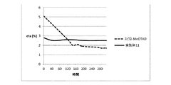
Classifications
-
- H—ELECTRICITY
- H10—SEMICONDUCTOR DEVICES; ELECTRIC SOLID-STATE DEVICES NOT OTHERWISE PROVIDED FOR
- H10K—ORGANIC ELECTRIC SOLID-STATE DEVICES
- H10K85/00—Organic materials used in the body or electrodes of devices covered by this subclass
- H10K85/60—Organic compounds having low molecular weight
- H10K85/649—Aromatic compounds comprising a hetero atom
- H10K85/657—Polycyclic condensed heteroaromatic hydrocarbons
- H10K85/6572—Polycyclic condensed heteroaromatic hydrocarbons comprising only nitrogen in the heteroaromatic polycondensed ring system, e.g. phenanthroline or carbazole
-
- H—ELECTRICITY
- H01—ELECTRIC ELEMENTS
- H01G—CAPACITORS; CAPACITORS, RECTIFIERS, DETECTORS, SWITCHING DEVICES, LIGHT-SENSITIVE OR TEMPERATURE-SENSITIVE DEVICES OF THE ELECTROLYTIC TYPE
- H01G9/00—Electrolytic capacitors, rectifiers, detectors, switching devices, light-sensitive or temperature-sensitive devices; Processes of their manufacture
- H01G9/20—Light-sensitive devices
- H01G9/2059—Light-sensitive devices comprising an organic dye as the active light absorbing material, e.g. adsorbed on an electrode or dissolved in solution
-
- C—CHEMISTRY; METALLURGY
- C07—ORGANIC CHEMISTRY
- C07D—HETEROCYCLIC COMPOUNDS
- C07D455/00—Heterocyclic compounds containing quinolizine ring systems, e.g. emetine alkaloids, protoberberine; Alkylenedioxy derivatives of dibenzo [a, g] quinolizines, e.g. berberine
- C07D455/03—Heterocyclic compounds containing quinolizine ring systems, e.g. emetine alkaloids, protoberberine; Alkylenedioxy derivatives of dibenzo [a, g] quinolizines, e.g. berberine containing quinolizine ring systems directly condensed with at least one six-membered carbocyclic ring, e.g. protoberberine; Alkylenedioxy derivatives of dibenzo [a, g] quinolizines, e.g. berberine
-
- H—ELECTRICITY
- H01—ELECTRIC ELEMENTS
- H01G—CAPACITORS; CAPACITORS, RECTIFIERS, DETECTORS, SWITCHING DEVICES, LIGHT-SENSITIVE OR TEMPERATURE-SENSITIVE DEVICES OF THE ELECTROLYTIC TYPE
- H01G9/00—Electrolytic capacitors, rectifiers, detectors, switching devices, light-sensitive or temperature-sensitive devices; Processes of their manufacture
- H01G9/20—Light-sensitive devices
- H01G9/2022—Light-sensitive devices characterized by he counter electrode
-
- H—ELECTRICITY
- H01—ELECTRIC ELEMENTS
- H01G—CAPACITORS; CAPACITORS, RECTIFIERS, DETECTORS, SWITCHING DEVICES, LIGHT-SENSITIVE OR TEMPERATURE-SENSITIVE DEVICES OF THE ELECTROLYTIC TYPE
- H01G9/00—Electrolytic capacitors, rectifiers, detectors, switching devices, light-sensitive or temperature-sensitive devices; Processes of their manufacture
- H01G9/20—Light-sensitive devices
- H01G9/2027—Light-sensitive devices comprising an oxide semiconductor electrode
-
- H—ELECTRICITY
- H10—SEMICONDUCTOR DEVICES; ELECTRIC SOLID-STATE DEVICES NOT OTHERWISE PROVIDED FOR
- H10K—ORGANIC ELECTRIC SOLID-STATE DEVICES
- H10K19/00—Integrated devices, or assemblies of multiple devices, comprising at least one organic element specially adapted for rectifying, amplifying, oscillating or switching, covered by group H10K10/00
- H10K19/10—Integrated devices, or assemblies of multiple devices, comprising at least one organic element specially adapted for rectifying, amplifying, oscillating or switching, covered by group H10K10/00 comprising field-effect transistors
-
- H—ELECTRICITY
- H10—SEMICONDUCTOR DEVICES; ELECTRIC SOLID-STATE DEVICES NOT OTHERWISE PROVIDED FOR
- H10K—ORGANIC ELECTRIC SOLID-STATE DEVICES
- H10K30/00—Organic devices sensitive to infrared radiation, light, electromagnetic radiation of shorter wavelength or corpuscular radiation
- H10K30/30—Organic devices sensitive to infrared radiation, light, electromagnetic radiation of shorter wavelength or corpuscular radiation comprising bulk heterojunctions, e.g. interpenetrating networks of donor and acceptor material domains
- H10K30/353—Organic devices sensitive to infrared radiation, light, electromagnetic radiation of shorter wavelength or corpuscular radiation comprising bulk heterojunctions, e.g. interpenetrating networks of donor and acceptor material domains comprising blocking layers, e.g. exciton blocking layers
-
- H—ELECTRICITY
- H10—SEMICONDUCTOR DEVICES; ELECTRIC SOLID-STATE DEVICES NOT OTHERWISE PROVIDED FOR
- H10K—ORGANIC ELECTRIC SOLID-STATE DEVICES
- H10K30/00—Organic devices sensitive to infrared radiation, light, electromagnetic radiation of shorter wavelength or corpuscular radiation
- H10K30/80—Constructional details
- H10K30/81—Electrodes
- H10K30/82—Transparent electrodes, e.g. indium tin oxide [ITO] electrodes
-
- H—ELECTRICITY
- H10—SEMICONDUCTOR DEVICES; ELECTRIC SOLID-STATE DEVICES NOT OTHERWISE PROVIDED FOR
- H10K—ORGANIC ELECTRIC SOLID-STATE DEVICES
- H10K85/00—Organic materials used in the body or electrodes of devices covered by this subclass
- H10K85/10—Organic polymers or oligomers
- H10K85/111—Organic polymers or oligomers comprising aromatic, heteroaromatic, or aryl chains, e.g. polyaniline, polyphenylene or polyphenylene vinylene
-
- H—ELECTRICITY
- H10—SEMICONDUCTOR DEVICES; ELECTRIC SOLID-STATE DEVICES NOT OTHERWISE PROVIDED FOR
- H10K—ORGANIC ELECTRIC SOLID-STATE DEVICES
- H10K85/00—Organic materials used in the body or electrodes of devices covered by this subclass
- H10K85/50—Organic perovskites; Hybrid organic-inorganic perovskites [HOIP], e.g. CH3NH3PbI3
-
- H—ELECTRICITY
- H10—SEMICONDUCTOR DEVICES; ELECTRIC SOLID-STATE DEVICES NOT OTHERWISE PROVIDED FOR
- H10K—ORGANIC ELECTRIC SOLID-STATE DEVICES
- H10K85/00—Organic materials used in the body or electrodes of devices covered by this subclass
- H10K85/60—Organic compounds having low molecular weight
- H10K85/631—Amine compounds having at least two aryl rest on at least one amine-nitrogen atom, e.g. triphenylamine
- H10K85/633—Amine compounds having at least two aryl rest on at least one amine-nitrogen atom, e.g. triphenylamine comprising polycyclic condensed aromatic hydrocarbons as substituents on the nitrogen atom
-
- H—ELECTRICITY
- H10—SEMICONDUCTOR DEVICES; ELECTRIC SOLID-STATE DEVICES NOT OTHERWISE PROVIDED FOR
- H10K—ORGANIC ELECTRIC SOLID-STATE DEVICES
- H10K10/00—Organic devices specially adapted for rectifying, amplifying, oscillating or switching; Organic capacitors or resistors having potential barriers
- H10K10/40—Organic transistors
- H10K10/46—Field-effect transistors, e.g. organic thin-film transistors [OTFT]
- H10K10/462—Insulated gate field-effect transistors [IGFETs]
- H10K10/484—Insulated gate field-effect transistors [IGFETs] characterised by the channel regions
-
- H—ELECTRICITY
- H10—SEMICONDUCTOR DEVICES; ELECTRIC SOLID-STATE DEVICES NOT OTHERWISE PROVIDED FOR
- H10K—ORGANIC ELECTRIC SOLID-STATE DEVICES
- H10K2102/00—Constructional details relating to the organic devices covered by this subclass
- H10K2102/10—Transparent electrodes, e.g. using graphene
- H10K2102/101—Transparent electrodes, e.g. using graphene comprising transparent conductive oxides [TCO]
- H10K2102/102—Transparent electrodes, e.g. using graphene comprising transparent conductive oxides [TCO] comprising tin oxides, e.g. fluorine-doped SnO2
-
- H—ELECTRICITY
- H10—SEMICONDUCTOR DEVICES; ELECTRIC SOLID-STATE DEVICES NOT OTHERWISE PROVIDED FOR
- H10K—ORGANIC ELECTRIC SOLID-STATE DEVICES
- H10K50/00—Organic light-emitting devices
- H10K50/10—OLEDs or polymer light-emitting diodes [PLED]
- H10K50/11—OLEDs or polymer light-emitting diodes [PLED] characterised by the electroluminescent [EL] layers
-
- Y—GENERAL TAGGING OF NEW TECHNOLOGICAL DEVELOPMENTS; GENERAL TAGGING OF CROSS-SECTIONAL TECHNOLOGIES SPANNING OVER SEVERAL SECTIONS OF THE IPC; TECHNICAL SUBJECTS COVERED BY FORMER USPC CROSS-REFERENCE ART COLLECTIONS [XRACs] AND DIGESTS
- Y02—TECHNOLOGIES OR APPLICATIONS FOR MITIGATION OR ADAPTATION AGAINST CLIMATE CHANGE
- Y02E—REDUCTION OF GREENHOUSE GAS [GHG] EMISSIONS, RELATED TO ENERGY GENERATION, TRANSMISSION OR DISTRIBUTION
- Y02E10/00—Energy generation through renewable energy sources
- Y02E10/50—Photovoltaic [PV] energy
- Y02E10/542—Dye sensitized solar cells
-
- Y—GENERAL TAGGING OF NEW TECHNOLOGICAL DEVELOPMENTS; GENERAL TAGGING OF CROSS-SECTIONAL TECHNOLOGIES SPANNING OVER SEVERAL SECTIONS OF THE IPC; TECHNICAL SUBJECTS COVERED BY FORMER USPC CROSS-REFERENCE ART COLLECTIONS [XRACs] AND DIGESTS
- Y02—TECHNOLOGIES OR APPLICATIONS FOR MITIGATION OR ADAPTATION AGAINST CLIMATE CHANGE
- Y02E—REDUCTION OF GREENHOUSE GAS [GHG] EMISSIONS, RELATED TO ENERGY GENERATION, TRANSMISSION OR DISTRIBUTION
- Y02E10/00—Energy generation through renewable energy sources
- Y02E10/50—Photovoltaic [PV] energy
- Y02E10/549—Organic PV cells
-
- Y—GENERAL TAGGING OF NEW TECHNOLOGICAL DEVELOPMENTS; GENERAL TAGGING OF CROSS-SECTIONAL TECHNOLOGIES SPANNING OVER SEVERAL SECTIONS OF THE IPC; TECHNICAL SUBJECTS COVERED BY FORMER USPC CROSS-REFERENCE ART COLLECTIONS [XRACs] AND DIGESTS
- Y02—TECHNOLOGIES OR APPLICATIONS FOR MITIGATION OR ADAPTATION AGAINST CLIMATE CHANGE
- Y02P—CLIMATE CHANGE MITIGATION TECHNOLOGIES IN THE PRODUCTION OR PROCESSING OF GOODS
- Y02P70/00—Climate change mitigation technologies in the production process for final industrial or consumer products
- Y02P70/50—Manufacturing or production processes characterised by the final manufactured product
Landscapes
- Engineering & Computer Science (AREA)
- Chemical & Material Sciences (AREA)
- Materials Engineering (AREA)
- Power Engineering (AREA)
- Physics & Mathematics (AREA)
- Organic Chemistry (AREA)
- Spectroscopy & Molecular Physics (AREA)
- Microelectronics & Electronic Packaging (AREA)
- Electromagnetism (AREA)
- Photovoltaic Devices (AREA)
- Organic Low-Molecular-Weight Compounds And Preparation Thereof (AREA)
- Polyoxymethylene Polymers And Polymers With Carbon-To-Carbon Bonds (AREA)
- Nitrogen And Oxygen Or Sulfur-Condensed Heterocyclic Ring Systems (AREA)
- Health & Medical Sciences (AREA)
- Chemical Kinetics & Catalysis (AREA)
- Medicinal Chemistry (AREA)
- Polymers & Plastics (AREA)
- Heterocyclic Carbon Compounds Containing A Hetero Ring Having Oxygen Or Sulfur (AREA)
Abstract
本発明は、熱的に安定な式(I)のトリアンギュレンのp型伝導性オリゴマー及びポリマー並びにそれらを色素増感太陽電池に用いる使用に関する。The present invention relates to thermally stable p-type conducting oligomers and polymers of formula (I) triangulene and their use in dye-sensitized solar cells.
Description
発明の属する技術分野
本発明は、熱的に安定なトリアンギュレンのp型伝導性オリゴマー及びポリマー並びにそれらを有機エレクトロニクス、有機光電池、特に色素増感型ペロブスカイト系太陽電池に用いる使用に関する。
TECHNICAL FIELD The present invention relates to thermally stable p-type conductive oligomers and polymers of triangulene and their use in organic electronics, organic photovoltaic cells, particularly dye-sensitized perovskite solar cells.
有機エレクトロニクス及び有機光電池は、主に、有機半導体層に基づく電子部品を製造するための新たな材料及び製造プロセスの開発に関するものである。これらには、特定の有機電界効果トランジスタ(OFET)、有機エレクトロルミネッセンス素子(以下、「EL」デバイスと略す)及び有機太陽電池が含まれる。開発の大きな可能性は、例えば、記憶素子及び集積光電子デバイスにおける有機電界効果トランジスタに帰するものである。有機発光ダイオード(OLED)の形態のEL素子は、平坦な視覚表示装置を製造するための陰極線管及び液晶ディスプレイの代替として特に重要である。開発のための大きな可能性はまた、光誘起励起状態の最大輸送幅と高移動度(高励起子拡散長さ)を有する新規な有機材料に帰するものであり、従って、有利には、いわゆる励起子太陽電池における活性物質として使用するのに適している。かかる材料に基づく太陽電池を用いれば、一般に、非常に良好な量子収率を達成することが可能である。それぞれの使用条件の下で有利な特性、例えば、前述の用途に適した、良好な熱安定性及びUV安定性を有する有機半導体化合物に対する要求が強い。 Organic electronics and organic photovoltaic cells are primarily concerned with the development of new materials and manufacturing processes for manufacturing electronic components based on organic semiconductor layers. These include certain organic field effect transistors (OFETs), organic electroluminescent elements (hereinafter abbreviated as “EL” devices) and organic solar cells. The great potential for development is attributed, for example, to organic field effect transistors in storage elements and integrated optoelectronic devices. EL elements in the form of organic light emitting diodes (OLEDs) are particularly important as an alternative to cathode ray tubes and liquid crystal displays for producing flat visual display devices. The great potential for development is also attributed to new organic materials with a maximum transport width and high mobility (high exciton diffusion length) of the photo-induced excited state, and thus advantageously the so-called Suitable for use as an active material in exciton solar cells. With solar cells based on such materials it is generally possible to achieve very good quantum yields. There is a strong demand for organic semiconductor compounds having advantageous properties under the respective conditions of use, for example, good thermal stability and UV stability suitable for the aforementioned applications.
色素増感型太陽電池(「DSSC」)は、現在最も効率的な代替太陽電池技術の1つである。この技術の液体変形例では、12%を上回る効率が報告されている(例えば、Graetzelら、Science 2011、334、629〜634頁)。 Dye-sensitized solar cells (“DSSC”) are currently one of the most efficient alternative solar cell technologies. In liquid variants of this technique, efficiencies greater than 12% have been reported (eg, Graetzel et al., Science 2011, 334, pages 629-634).
DSSCの構造は、一般に、透明導電層、作用電極で被覆された透明基板(例えば、ガラス)に基づくものである。n型伝導性金属酸化物、例えば、約2〜20μm厚さのナノ多孔質二酸化チタン層(TiO2)は、一般に、この電極に又はその近傍に適用されている。その表面に、光感受性色素、例えば、ルテニウム錯体又は有機色素の単層が、通常、順番に吸収され、これが光吸収によって励起状態に変換され得る。対向電極は、任意に、金属、例えば、白金の触媒層を、数μmの厚さで有し得る。DSSCの機能は、光が色素によって吸収され、電子が励起した色素からn型半導体金属酸化膜半導体に移動し、その表面でアノードに移行する事実に基づくものである。液体DSSCでは、2つの電極間の領域がレドックス電解質、例えば、ヨウ素(I2)及びヨウ化リチウム(LiI)の溶液で満たされており、このため、電池の前面及び背面の接点で確実に光電流を集めることができる。 The structure of DSSC is generally based on a transparent substrate (eg, glass) coated with a transparent conductive layer and a working electrode. An n-type conductive metal oxide, for example, a nanoporous titanium dioxide layer (TiO 2 ) of about 2-20 μm thickness is generally applied to or near this electrode. On its surface, a monolayer of a photosensitive dye, such as a ruthenium complex or an organic dye, is usually absorbed in turn, which can be converted to an excited state by light absorption. The counter electrode may optionally have a catalyst layer of metal, for example platinum, with a thickness of a few μm. The function of DSSC is based on the fact that light is absorbed by the dye, the electrons move from the excited dye to the n-type semiconductor metal oxide semiconductor, and migrate to the anode on the surface. In liquid DSSCs, the area between the two electrodes is filled with a redox electrolyte, for example, a solution of iodine (I 2 ) and lithium iodide (LiI), so that light is reliably transmitted at the front and back contacts of the battery. Can collect current.
液体電解質を含む電池は、この技術のより広い使用を妨げる特別な欠点を有する。そのため、多くの場合、液体DSSCは、電極腐食や電解液漏れなどの深刻な問題を引き起こす有機液体電解質の使用に起因する耐久性の問題がある。従って、液体電解質の代わりに正孔伝導に使用され得る適切な代替物が探し求められている。その結果、様々な材料が、固体電解質/p型半導体としての適性について研究されてきた。 Batteries containing liquid electrolytes have special drawbacks that prevent wider use of this technology. Thus, in many cases, liquid DSSCs have durability problems due to the use of organic liquid electrolytes that cause serious problems such as electrode corrosion and electrolyte leakage. Accordingly, there is a need for suitable alternatives that can be used for hole conduction instead of liquid electrolytes. As a result, various materials have been studied for their suitability as solid electrolyte / p-type semiconductors.
様々な無機p型半導体、例えば、CuI、CuBr3(S(C4H9)2)又はCuSCNが、今日まで固体段階のDSSCでの使用が見出されてきた。CuIベースの固体DSSCを使用する場合、例えば、7%を上回る効率がHitoshi Sakamotoらによって報告されている(Organic Electronics 13 (2012), 514〜518頁)。 Various inorganic p-type semiconductor, for example, CuI, CuBr3 (S (C 4 H 9) 2) or CuSCN, have found use in a DSSC of the solid phase to date. For example, when using a CuI-based solid DSSC, efficiencies greater than 7% have been reported by Hitoshi Sakamoto et al. (Organic Electronics 13 (2012), pages 514-518).
正孔伝導性材料としてフッ素及び二フッ化錫ドープCsSnl3を含み且つ約10%の効率を示す固体DSSCがIn Chungらによって報告された(Nature 第485巻, 5月24日, 2012年, 486〜490頁)。特に、ヨウ化化合物の欠点は腐食性である。 A solid DSSC comprising fluorine and tin difluoride doped CsSnl 3 as hole conducting material and showing an efficiency of about 10% was reported by In Chung et al. (Nature 485, May 24, 2012, 486). ~ 490). In particular, the disadvantage of iodide compounds is corrosiveness.
低い分子量の有機p型半導体を用いて高い効率を達成することが可能である。例えば、WO98/48433A1号は、有機化合物、2,2’,7,7’−テトラキス(N,N−ジ−p−メトキシフェニル−アミン)−9,9’−スピロビフルオレン(”スピロ−MeOTAD”)を正孔輸送材料としてDSSCに用いる使用を報告している。それにもかかわらず、スピロ−MeOTADの熱安定性は、まだ改善の余地がある。 High efficiencies can be achieved using low molecular weight organic p-type semiconductors. For example, WO 98/48433 A1 describes an organic compound, 2,2 ′, 7,7′-tetrakis (N, N-di-p-methoxyphenyl-amine) -9,9′-spirobifluorene (“spiro-MeOTAD”). ") Is used for DSSC as a hole transport material. Nevertheless, the thermal stability of Spiro-MeOTAD still has room for improvement.
有機ポリマーも非腐食性の固体p型半導体として使用される。その例としては、ポリピロール、ポリ(3,4−エチレンジオキシチオフェン)、カルバゾール系ポリマー、ポリアニリン、ポリ(4−ウンデシル−2,2’−ビチオフェン)、ポリ(3−オクチルチオフェン)、ポリ(トリフェニルジアミン)及びポリ(N−ビニルカルバゾール)が挙げられる。ポリ(N−ビニルカルバゾール)の場合、ポリマーが典型的には純粋な形で使用されていないが、通常、添加剤との混合物で使用されていても、効率は、インサイチュで重合された、PEDOT(ポリ(3,4−エチレンジオキシチオフェン)を用いて2%に達し、更に、2.9%の効率も達成された(Xiaら、J. Phys. Chem. C 2008, 112, 11569)。Peter, K.はAppl. Phys. A 2004, 79, 65において概念を記載しており、その際、ポリマーのp型半導体がRu色素に直接結合されている。 Organic polymers are also used as non-corrosive solid p-type semiconductors. Examples thereof include polypyrrole, poly (3,4-ethylenedioxythiophene), carbazole polymer, polyaniline, poly (4-undecyl-2,2′-bithiophene), poly (3-octylthiophene), poly (tri Phenyldiamine) and poly (N-vinylcarbazole). In the case of poly (N-vinylcarbazole), the polymer is typically not used in pure form, but the efficiency is usually in-situ polymerized PEDOT, even when used in admixture with additives. (Using poly (3,4-ethylenedioxythiophene), it reached 2% and an efficiency of 2.9% was also achieved (Xia et al., J. Phys. Chem. C 2008, 112, 11569). Peter, K. describes the concept in Appl. Phys. A 2004, 79, 65, where the polymer p-type semiconductor is bonded directly to the Ru dye.
WO2007/031165A2号は、以下の式(1)及び(2)

の化合物、並びにこれらの化合物を、エレクトロルミネセンスデバイス、例えば、OLED及びOFETに用いる使用を記載している。具体的な化合物は、中心コアとしてたった1つの(ヘテロ)トリアンギュレン部分を含む。
WO2007 / 031165A2 describes the following formulas (1) and (2)
And the use of these compounds in electroluminescent devices such as OLEDs and OFETs. Specific compounds contain only one (hetero) triangulene moiety as the central core.
Tetrahedron 65 (2009年), 4455〜4463頁は、周辺枝としてのカルバゾールデンドロンと中心コアとしてのトリアンギュレンを有する星型ドナー−アクセプターデンドリマーの合成、特性評価及びエレクトロルミネセンス特性を記載している。 Tetrahedron 65 (2009), pages 4455-4463 describe the synthesis, characterization and electroluminescence properties of star-type acceptor-dendrimers with carbazole dendrons as peripheral branches and triangulene as central core. Yes.
J. Mater. Chem., 2012, 22, 15397〜15404頁は、エレクトロルミネセントデバイスのための正孔輸送材料としてのブリッジドトリアリールアミンスターバーストオリゴマーを記載している。この論文は、とりわけ、以下の式:
この文書では、オリゴマーの非線形構造が、用途特性、例えば、良好な溶解性及び高い熱耐久性にとって非常に重要であると考えられる。著者は、DSC(示差走査熱量測定)測定以外のデバイスデータを示していない。しかしながら、DSCは、デバイスの条件がはるかに複雑である(例えば、異なる材料/インタフェース)ため、多くの場合、デバイスの性能と相関することができない。 In this document, the non-linear structure of the oligomer is considered very important for application properties such as good solubility and high thermal durability. The author shows no device data other than DSC (Differential Scanning Calorimetry) measurements. However, DSCs often cannot correlate with device performance because the device conditions are much more complex (eg, different materials / interfaces).
固体DSSCの製造における新たな進展は、有機金属ペロブスカイトを集光性化合物として用いる使用である。H.-S. Kimらは、Scientific Reports, 2 : 59, DOI: 10.1038 / srep00591において、9%を超える効率を有するヨウ化鉛ペロブスカイト増感型太陽電池を記載している。これらの電池では、メチルアンモニウムヨウ化鉛のペロブスカイトナノ粒子は、透明n型半導体としてのメソポーラスTiO2とp型正孔伝導体としてのスピロMeOTADとを組み合わせた吸収体材料として使用されている。 A new advance in the production of solid DSSCs is the use of organometallic perovskites as light collecting compounds. H.-S. Kim et al., In Scientific Reports, 2:59, DOI: 10.1038 / srep00591, describe lead iodide perovskite sensitized solar cells with efficiencies greater than 9%. In these batteries, perovskite nanoparticles of methylammonium lead iodide are used as an absorber material combining mesoporous TiO 2 as a transparent n-type semiconductor and spiro MeOTAD as a p-type hole conductor.
M. M. Leeらは、Sciencexpress, 4 October 2012, 10. 1126 / science.1228604において、メソ超構造有機金属ハロゲン化物ペロブスカイトに基づくハイブリッド太陽電池を記載している。これらの電池では、メソポーラスアルミナが、二酸化チタンの代わりに使用されている。これらの電池では、Al2O3はn型酸化物として機能しないが、デバイスが構成される際のメソスケールの「足場」の役目を果たす。従って、著者らは、もはやデバイスを「増感」太陽電池として示さず、2成分ハイブリッド太陽電池又は「メソ超構造太陽電池」として示す。 MM Lee et al., In Siencexpress, 4 October 2012, 10. 1126 / science. 1228604, describe hybrid solar cells based on mesosuperstructured organometallic halide perovskites. In these batteries, mesoporous alumina is used instead of titanium dioxide. In these batteries, Al 2 O 3 does not function as an n-type oxide, but serves as a mesoscale “scaffold” when the device is constructed. Thus, the authors no longer indicate the device as a “sensitized” solar cell, but as a two-component hybrid solar cell or “meso superstructure solar cell”.
Jeong-Hyeok Imらは、Nanoscale Research lettersにおいて、ナノ結晶2Hペロブスカイト型新規増感剤(CH3CH2NH3)Pbl3の合成、構造及び光起電性を記載している。 Jeong-Hyeok Im et al. Describe in Nanoscale Research letters the synthesis, structure and photovoltaic properties of a novel nanocrystalline 2H perovskite type sensitizer (CH 3 CH 2 NH 3 ) Pbl 3 .
本発明の課題は、p型半導体として、様々な適用分野、特に、太陽電池、とりわけ、固体状態の正孔伝導体に基づく太陽電池において有利に使用され得る化合物を提供することである。これらの適用特性に関して、これらの化合物は、良好な熱安定性と良好な正孔導電性を有するべきである。 The object of the present invention is to provide compounds which can be used advantageously as p-type semiconductors in various applications, in particular in solar cells, in particular solar cells based on solid state hole conductors. With respect to these application properties, these compounds should have good thermal stability and good hole conductivity.
ここで驚くことに、この課題が、直鎖状トリアンギュレンオリゴマー及びポリマーによって達成されることが判明した。 Surprisingly, it has now been found that this task is achieved by linear triangulene oligomers and polymers.
発明の概要
本発明の第1の態様によれば、一般式I
nは0〜100であり、
X1、X2、X3、X4、及びX5は互いに独立して水素、F、Cl、Br、I、CN、B(ORc)2、
ヒドロキシ、メルカプト、ニトロ、シアナト、チオシアナト、ホルミル、アシル、カルボキシ、カルボキシレート、アルキルカルボニルオキシ、カルバモイル、アルキルアミノカルボニル、ジアルキルアミノカルボニル、スルホ、スルホネート、スルホアミノ、スルファモイル、アルキルスルホニル、アリールスルホニル、アミジノ、NE1E2から選択され、ここで、E1及びE2はそれぞれ独立して水素、アルキル、シクロアルキル、ヘテロシクロアルキル、アリール又はヘタリールから選択され、
それぞれの場合に、非置換又は置換のアルキル、アルコキシ、アルキルチオ、(モノアルキル)アミノ、(ジアルキル)アミノ、シクロアルキル、シクロアルコキシ、シクロアルキルチオ、(モノシクロアルキル)アミノ、(ジシクロアルキル)アミノ、ヘテロシクロアルキル、ヘテロシクロアルコキシ、ヘテロシクロ−アルキルチオ、(モノヘテロシクロアルキル)アミノ、(ジヘテロシクロアルキル)アミノ、アリール、アリールオキシ、アリールチオ、(モノアリール)アミノ、(ジアリール)アミノ、ヘタリール、ヘタリールオキシ、ヘタリールチオ、(モノ−ヘタリール)アミノ及び(ジヘタリール)アミノから選択され、
ここで、Rcはそれぞれの場合に非置換又は置換のアルキル、シクロアルキル又はアリールから選択されるか、又は2つの基Rcが一緒にそれぞれの場合に非置換又は置換のC2〜C10−アルキレン、C3〜C6−シクロアルキレン及びC6〜C14−アリーレンから選択される二価の橋かけ基を形成してよく、ここで、C2〜C10−アルキレン、C3〜C6−シクロアルキレン及びC6〜C14−アリーレンは、1つ以上の同一又は異なるC1〜C12−アルキル基を有してよく、
Ra及びRbは、互いに独立して、水素及び非置換のC1〜C6−アルキルから選択され、
R1、R2、R3、R4、R5、R6、R13、R14、R15、R16、及び存在する場合、R7、R8、R9、R10、R11及びR12は、互いに独立して、水素、及びそれぞれの場合に非置換又は置換のアルキル、アルコキシ、アルケニル、アルカジエニル、アルキニル、シクロアルキル、シクロアルコキシ、ビシクロアルキル、シクロアルケニル、ヘテロシクロアルキル、ヘテロシクロアルキルオキシ、アリール、アリールオキシ、ヘテロアリール及びヘテロアリールオキシから選択される)
の化合物が提供される。
SUMMARY OF THE INVENTION According to a first aspect of the present invention, the general formula I
n is 0-100,
X 1 , X 2 , X 3 , X 4 , and X 5 are independently of each other hydrogen, F, Cl, Br, I, CN, B (OR c ) 2 ,
Hydroxy, mercapto, nitro, cyanato, thiocyanato, formyl, acyl, carboxy, carboxylate, alkylcarbonyloxy, carbamoyl, alkylaminocarbonyl, dialkylaminocarbonyl, sulfo, sulfonate, sulfoamino, sulfamoyl, alkylsulfonyl, arylsulfonyl, amidino, NE 1 E 2 , wherein E 1 and E 2 are each independently selected from hydrogen, alkyl, cycloalkyl, heterocycloalkyl, aryl or hetaryl;
In each case, unsubstituted or substituted alkyl, alkoxy, alkylthio, (monoalkyl) amino, (dialkyl) amino, cycloalkyl, cycloalkoxy, cycloalkylthio, (monocycloalkyl) amino, (dicycloalkyl) amino, Heterocycloalkyl, heterocycloalkoxy, heterocyclo-alkylthio, (monoheterocycloalkyl) amino, (diheterocycloalkyl) amino, aryl, aryloxy, arylthio, (monoaryl) amino, (diaryl) amino, hetaryl, hetaryl Selected from oxy, hetarylthio, (mono-hetaryl) amino and (dihetaryl) amino;
Wherein R c is in each case selected from unsubstituted or substituted alkyl, cycloalkyl or aryl, or the two groups R c together in each case are unsubstituted or substituted C 2 -C 10 May form a divalent bridging group selected from -alkylene, C 3 -C 6 -cycloalkylene and C 6 -C 14 -arylene, wherein C 2 -C 10 -alkylene, C 3 -C 6 - cycloalkylene and C 6 -C 14 - arylene, one or more identical or different C 1 -C 12 - may have an alkyl group,
R a and R b are independently of one another selected from hydrogen and unsubstituted C 1 -C 6 -alkyl;
R 1 , R 2 , R 3 , R 4 , R 5 , R 6 , R 13 , R 14 , R 15 , R 16 , and if present, R 7 , R 8 , R 9 , R 10 , R 11 and R 12 is independently of one another hydrogen and, in each case, unsubstituted or substituted alkyl, alkoxy, alkenyl, alkadienyl, alkynyl, cycloalkyl, cycloalkoxy, bicycloalkyl, cycloalkenyl, heterocycloalkyl, heterocycloalkyl Selected from oxy, aryl, aryloxy, heteroaryl and heteroaryloxy)
Are provided.
本発明の更なる対象は、上記及び下記に定義される一般式(I)の少なくとも1種の化合物を含む組成物に関する。 A further subject of the present invention relates to a composition comprising at least one compound of general formula (I) as defined above and below.
本発明の更なる対象は、式(I)の化合物の製造方法に関する。 A further subject of the present invention relates to a process for the preparation of the compounds of formula (I).
本発明の更なる対象は、色素増感型光電変換素子及び光電セル、好ましくはかかる素子を含む、太陽電池に関する。 A further subject of the present invention relates to a dye-sensitized photoelectric conversion element and a photoelectric cell, preferably a solar cell comprising such an element.
好ましい実施態様は、色素増感型光電変換素子であって、
− 作用電極(アノード)の一部であるか又はそれを形成する導電層、
− 半導体金属酸化物及び発色物質を含む感光層、
− 上記及び下記で定義される式(I)の少なくとも1種の化合物を含む電荷輸送層、
− 対向電極(カソード)の一部であるか又はそれを形成する導電層
を含む、前記色素増感型光電変換素子である。
A preferred embodiment is a dye-sensitized photoelectric conversion element,
A conductive layer that is part of or forms part of the working electrode (anode);
A photosensitive layer comprising a semiconductor metal oxide and a coloring material,
A charge transport layer comprising at least one compound of formula (I) as defined above and below,
-The dye-sensitized photoelectric conversion element which is a part of the counter electrode (cathode) or includes a conductive layer forming the same.
本発明の更なる対象は、ペロブスカイト型光電変換素子及び光電セル、好ましくは、かかる素子を含む、太陽電池に関する。 A further subject matter of the present invention relates to a perovskite photoelectric conversion element and a photoelectric cell, preferably a solar cell comprising such an element.
光電セルは、色素増感型光電変換素子を含み且つ電気回路の一部である。 The photoelectric cell includes a dye-sensitized photoelectric conversion element and is a part of an electric circuit.
好ましい実施態様は、ペロブスカイト型光電変換素子であって、
− 作用電極(アノード)の一部であるか又はそれを形成する導電層、
− ペロブスカイト吸収材料を含む感光層、
− 上記及び下記で定義される少なくとも1種の式(I)の化合物を含む電荷輸送層、
− 対向電極(カソード)の一部であるか又はそれを形成する導電層
を含む、前記ペロブスカイト型光電変換素子である。
A preferred embodiment is a perovskite photoelectric conversion element,
A conductive layer that is part of or forms part of the working electrode (anode);
A photosensitive layer comprising a perovskite absorbing material,
A charge transport layer comprising at least one compound of formula (I) as defined above and below,
-The perovskite photoelectric conversion element, which is a part of the counter electrode (cathode) or includes a conductive layer forming the same.
本発明の更なる対象は、上記及び下記で定義される式(I)の化合物又は式(I)の少なくとも1種の化合物を含む組成物を、色素増感型光電変換素子に用いる使用に関する。これは特に、式(I)の化合物又は式(I)の少なくとも1種の化合物を含む組成物を、正孔輸送材料(p型半導体)として色素増感型太陽電池に用いる使用に関する。 A further subject of the present invention relates to the use of a composition comprising a compound of formula (I) or at least one compound of formula (I) as defined above and below for use in a dye-sensitized photoelectric conversion element. This particularly relates to the use of a compound of formula (I) or a composition comprising at least one compound of formula (I) in a dye-sensitized solar cell as a hole transport material (p-type semiconductor).
本発明の更なる対象は、上記及び下記に定義される式(I)の化合物又は式(I)の少なくとも1種の化合物を含む組成物を、有機エレクトロニクス用途又は有機太陽電池、特に有機電界効果トランジスタ及び有機太陽電池に用いる使用に関する。 A further subject of the present invention is the use of a compound of formula (I) as defined above and below or a composition comprising at least one compound of formula (I) for organic electronics applications or organic solar cells, in particular organic field effects. The present invention relates to use for transistors and organic solar cells.
図面の簡単な説明
図1は、正孔輸送材料(HTM)として実施例11のトリアンギュレンモノマーを含むDSSC又は正孔輸送材料(HTM)としてスピロMeOTADを含むDSSCの寿命にわたる効率(η)の比較を示す。
BRIEF DESCRIPTION OF THE DRAWINGS FIG. 1 shows the efficiency (η) over the lifetime of a DSSC comprising the triangulene monomer of Example 11 as a hole transport material (HTM) or a DSSC comprising spiro MeOTAD as a hole transport material (HTM). A comparison is shown.
発明の詳細な説明
好ましくは、一般式(I)の化合物は直鎖状構造を有する。本発明の意味において、直鎖状構造は、トリアンギュレン繰り返し単位が直接結合を介して2つを上回る更なるトリアンギュレン繰り返し単位に全く結合されていないことを意味する。特に、一般式(I)の化合物は、例えば、J. Mater. Chem., 2012年, 22, 15397〜15404頁に記載されるようなスターバースト構造を有していない。
DETAILED DESCRIPTION OF THE INVENTION Preferably, the compound of general formula (I) has a linear structure. In the sense of the present invention, a linear structure means that the triangulene repeat unit is not bound to any more than two further triangulene repeat units via a direct bond. In particular, the compound of the general formula (I) does not have a starburst structure as described in, for example, J. Mater. Chem., 2012, 22, 15397-15404.
本発明の文脈において、「ペロブスカイト型光電変換素子」との表現は、ペロブスカイト成分がn型半導体金属酸化物(例えば、二酸化チタン)と組み合わせて使用される素子並びにペロブスカイト成分が吸収体としてだけでなく、n型導電体としても使用される素子を意味する。これらのセルでは、ペロブスカイト成分は、n型酸化物(例えば、Al2O3)として機能しない担体材料と組み合わせて使用される。 In the context of the present invention, the expression “perovskite-type photoelectric conversion device” means not only an element in which a perovskite component is used in combination with an n-type semiconductor metal oxide (for example, titanium dioxide), but also a perovskite component as an absorber. , Means an element also used as an n-type conductor. In these cells, the perovskite component is used in combination with a carrier material that does not function as an n-type oxide (eg, Al 2 O 3 ).
「ハロゲン」との表現は、それぞれの場合に、フッ素、臭素、塩素又はヨウ素、特に塩素、臭素又はヨウ素を意味する。 The expression “halogen” means in each case fluorine, bromine, chlorine or iodine, in particular chlorine, bromine or iodine.
本願明細書で使用される、「非置換又は置換のアルキル、アルケニル、アルカジエニル、アルキニル、シクロアルキル、ビシクロアルキル、シクロアルケニル、ヘテロシクロアルキル、アリール又はヘテロアリール」との表現は、非置換又は置換のアルキル、非置換又は置換のアルケニル、非置換又は置換のアルカジエニル、非置換又は置換のアルキニル、非置換又は置換のシクロアルキル、非置換又は置換のビシクロアルキル、非置換又は置換のシクロアルケニル、非置換又は置換のヘテロシクロアルキル、非置換又は置換のアリール又は非置換又は置換のヘテロアリールを指す。 As used herein, the expression “unsubstituted or substituted alkyl, alkenyl, alkadienyl, alkynyl, cycloalkyl, bicycloalkyl, cycloalkenyl, heterocycloalkyl, aryl or heteroaryl” refers to unsubstituted or substituted Alkyl, unsubstituted or substituted alkenyl, unsubstituted or substituted alkadienyl, unsubstituted or substituted alkynyl, unsubstituted or substituted cycloalkyl, unsubstituted or substituted bicycloalkyl, unsubstituted or substituted cycloalkenyl, unsubstituted or Refers to substituted heterocycloalkyl, unsubstituted or substituted aryl or unsubstituted or substituted heteroaryl.
本発明の文脈において、「非置換又は置換アルキル、アルコキシ、アルキルチオ、(モノアルキル)アミノ、(ジアルキル)アミノ、シクロアルキル、シクロアルコキシ、シクロアルキルチオ、(モノシクロアルキル)アミノ、(ジシクロアルキル)アミノ、ヘテロシクロアルキル、ヘテロシクロアルコキシ、ヘテロシクロアルキルチオ、(モノヘテロシクロアルキル)アミノ、(ジヘテロシクロアルキル)アミノ、アリール、アリールオキシ、アリールチオ、(モノアリール)アミノ、(ジアリール)アミノ、ヘタリール、ヘタリールオキシ、ヘタリールチオ、(モノヘタリール)アミノ及び(ジヘタリール)アミノ」との表現は、非置換又は置換のアルキル、非置換又は置換のアルコキシ、非置換又は置換のアルキルチオ、非置換又は置換の(モノアルキル)アミノ、非置換又は置換の(ジアルキル)アミノ、非置換又は置換のシクロアルキル、非置換又は置換のシクロアルコキシ、非置換又は置換のシクロアルキルチオ、非置換又は置換の(モノシクロアルキル)アミノ、非置換又は置換の(ジシクロアルキル)アミノ、非置換又は置換のヘテロシクロアルキル、非置換又は置換のヘテロシクロアルコキシ、非置換又は置換のヘテロシクロアルキルチオ、非置換又は置換の(モノヘテロシクロアルキル)アミノ、非置換又は置換の(ジヘテロシクロアルキル)アミノ、非置換又は置換のアリール、非置換又は置換のアリールオキシ、非置換又は置換のアリールチオ、非置換又は置換の(モノアリール)アミノ、非置換又は置換の(ジアリール)アミノ、非置換又は置換のヘタリール、非置換又は置換のヘタリールオキシ、非置換又は置換のヘタリールチオ、非置換又は置換の(モノヘタリール)アミノ及び非置換又は置換の(ジヘタリール)アミノを表す。 In the context of the present invention, “unsubstituted or substituted alkyl, alkoxy, alkylthio, (monoalkyl) amino, (dialkyl) amino, cycloalkyl, cycloalkoxy, cycloalkylthio, (monocycloalkyl) amino, (dicycloalkyl) amino” , Heterocycloalkyl, heterocycloalkoxy, heterocycloalkylthio, (monoheterocycloalkyl) amino, (diheterocycloalkyl) amino, aryl, aryloxy, arylthio, (monoaryl) amino, (diaryl) amino, hetaryl, hetaryl The expressions "reeloxy, hetarylthio, (monohetaryl) amino and (dihetaryl) amino" are unsubstituted or substituted alkyl, unsubstituted or substituted alkoxy, unsubstituted or substituted alkylthio, unsubstituted or substituted. (Monoalkyl) amino, unsubstituted or substituted (dialkyl) amino, unsubstituted or substituted cycloalkyl, unsubstituted or substituted cycloalkoxy, unsubstituted or substituted cycloalkylthio, unsubstituted or substituted (monocycloalkyl) ) Amino, unsubstituted or substituted (dicycloalkyl) amino, unsubstituted or substituted heterocycloalkyl, unsubstituted or substituted heterocycloalkoxy, unsubstituted or substituted heterocycloalkylthio, unsubstituted or substituted (monohetero) Cycloalkyl) amino, unsubstituted or substituted (diheterocycloalkyl) amino, unsubstituted or substituted aryl, unsubstituted or substituted aryloxy, unsubstituted or substituted arylthio, unsubstituted or substituted (monoaryl) amino , Unsubstituted or substituted (diaryl) amino, unsubstituted or substituted Over represented Le, unsubstituted or substituted hetaryloxy, unsubstituted or substituted hetarylthio, unsubstituted or substituted (Monohetariru) amino and unsubstituted or substituted with (Jihetariru) amino.
本発明の文脈において、「アルキル」との表現は、直鎖状又は分枝鎖状のアルキル基を含む。アルキルは好ましくはC1〜C30−アルキル、更に好ましくはC1〜C20−アルキル、最も好ましくはC1〜C12−アルキルである。アルキル基の例は、特に、メチル、エチル、n−プロピル、イソプロピル、n−ブチル、イソブチル、sec−ブチル、tert−ブチル、n−ペンチル、1−メチルブチル、1−エチルプロピル、ネオ−ペンチル、n−ヘキシル、1−メチルペンチル、2−メチルペンチル、1−エチルブチル、2−エチルブチル、n−ヘプチル、1−メチルヘキシル、2−メチルヘキシル、1−エチルペンチル、1−プロピルブチル、2−エチルペンチル、n−オクチル、1−メチルヘプチル、2−メチルヘプチル、1−エチルヘキシル、2−エチルヘキシル、1−プロピルペンチル、2−プロピルペンチル、n−ノニル、1−メチルオクチル、2−メチルオクチル、1−エチルヘプチル、2−エチルヘプチル、1−プロピルヘキシル、2−プロピルヘキシル、1−ブチルペンチル、n−デシル、2−メチルデシル、1−メチルノニル、2−メチルノニル、1−エチルオクチル、2−エチルオクチル、1−プロピルヘプチル、2−プロピルヘプチル、1−ブチルヘキシル、2−ブチルヘキシル、n−ウンデシル、2−エチルノニル、1−プロピルオクチル、2−プロピルオクチル、1−ブチルヘプチル、2−ブチルヘプチル、1−ペンチルヘキシル、n−ドデシル、2−エチルデシル、2−プロピルノニル、1−ブチルオクチル、2−ブチルオクチル、1−ペンチルヘプチル、2−ペンチルヘプチル、2−プロピルデシル、n−トリデシル、1−ペンチルオクチル、2−ペンチルオクチル、1−ヘキシルヘプチル、2−ブチルノニル、n−テトラデシル、1−ヘキシルオクチル、2−ヘキシルオクチル、2−ペンチルノニル、2−ヘキシルノニル、2−ペンチルデシル、2−ブチルデシル、n−ヘキサデシル、1−ヘプチルオクチル、2−ヘプチルノニル、2−ヘキシルデシル、2−ヘプチルデシル、n−オクタデシル、2−オクチルデシル、n−エイコシル、2−ノニルウンデシル、2−オクチルウンデシル、2−ヘプチルウンデシル、2−ヘキシルウンデシル、2−ペンチルウンデシル、2−ブチルウンデシル、2−プロピルウンデシル、2−エチルウンデシル、2−メチルウンデシル、2−デシルドデシル、2−ノニルドデシル、2−オクチルドデシル、2−ヘプチルドデシル、2−ヘキシルドデシル、2−ペンチルドデシル、2−ブチルドデシル、2−プロピルドデシル、2−エチルドデシル、2−メチルドデシル、2−ウンデシルトリデシル、2−デシルトリデシル、2−ノニルトリデシル、2−オクチルトリデシル、2−ヘプチルトリデシル、2−ヘキシルトリデシル、2−ペンチルトリデシル、2−ブチルトリデシル、2−プロピルトリデシル、2−エチルトリデシル、2−メチルトリデシル、2−ウンデシルテトラデシル、2−デシルテトラデシル、2−ノニルテトラデシル、2−オクチルテトラデシル、2−ヘチルテトラデシル(hetyltetradecyl)、2−ヘキシルテトラデシル、2−ペンチルテトラデシル、2−ブチルテトラデシル、2−プロピルテトラデシル、2−エチルテトラデシル、2−メチルテトラデシル、2−テトラデシルヘキサデシル、2−トリデシルヘキサデシル、2−ドデシルヘキサデシル、2−ウンデシルヘキサデシル、2−デシルヘキサデシル、2−ノニルヘキサデシル、2−オクチルヘキサデシル、2−ヘプチルヘキサデシル、2−ヘキシルヘキサデシル、2−ペンチルヘキサデシル、2−ブチルヘキサデシル、2−プロピルヘキサデシル、2−エチルヘキサデシル、2−メチルヘキサデシル、2−ドデシルオクタデシル、2−ウンデシルオクタデシル、2−デシルオクタデシル、2−ノニルオクタデシル、2−オクチルオクタデシル、2−ヘプチルオクタデシル、2−ヘキシルオクタデシル、2−ペンチルオクタデシル、2−ブチルオクタデシル、2−プロピルオクタデシル、2−エチルオクタデシル、2−メチルオクタデシル、2−デシルエイコサニル、2−ノニルエイコサニル、2−オクチルエイコサニル、2−ヘプチルエイコサニル、2−ヘキシルエイコサニル、2−ペンチルエイコサニル、2−ブチルエイコサニル、2−プロピルエイコサニル、2−エチルエイコサニル、2−メチルエイコサニル、2−オクタデシルドコサニル、2−ヘプタデシルドコサニル、2−ヘキサデシルドコサニル、2−ペンタデシルドコサニル、2−テトラデシルドコサニル、2−トリデシルドコサニル、2−ウンデシルドコサニル、2−デシルドコサニル、2−ノニルドコサニル、2−オクチルドコサニル、2−ヘプチルドコサニル、2−ヘキシルドコサニル、2−ペンチルドコサニル、2−ブチルドコサニル、2−プロピルドコサニル、2−エチルドコサニル、2−メチルドコサニル、2−ドコサニルテトラコサニル、2−ヘキサデシルテトラコサニル、2−ペンタデシルテトラコサニル、2−ペンタデシルテトラコサニル、2−テトラデシルテトラコサニル、2−トリデシルテトラコサニル、2−ドデシルテトラコサニル、2−ウンデシルテトラコサニル、2−デシルテトラコサニル、2−ノニルテトラコサニル、2−オクチルテトラコサニル、2−ヘプチルテトラコサニル、2−ヘキシルテトラコサニル、2−ペンチルテトラコサニル、2−ブチルテトラコサニル、2−プロピルテトラコサニル、2−エチルテトラコサニル、2−メチルテトラコサニル、2−ドデシルオクタコサニル、2−ウンデシルオクタコサニル、2−デシルオクタコサニル、2−ノニルオクタコサニル、2−オクチルオクタコサニル、2−ヘプチルオクタコサニル、2−ヘキシルオクタコサニル、2−ペンチルオクタコサニル、2−ブチルオクタコサニル、2−プロピルオクタコサニル、2−エチルオクタコサニル及び2−メチルオクタコサニルである。 In the context of the present invention, the expression “alkyl” includes straight-chain or branched alkyl groups. Alkyl is preferably C 1 -C 30 -alkyl, more preferably C 1 -C 20 -alkyl, most preferably C 1 -C 12 -alkyl. Examples of alkyl groups are in particular methyl, ethyl, n-propyl, isopropyl, n-butyl, isobutyl, sec-butyl, tert-butyl, n-pentyl, 1-methylbutyl, 1-ethylpropyl, neo-pentyl, n -Hexyl, 1-methylpentyl, 2-methylpentyl, 1-ethylbutyl, 2-ethylbutyl, n-heptyl, 1-methylhexyl, 2-methylhexyl, 1-ethylpentyl, 1-propylbutyl, 2-ethylpentyl, n-octyl, 1-methylheptyl, 2-methylheptyl, 1-ethylhexyl, 2-ethylhexyl, 1-propylpentyl, 2-propylpentyl, n-nonyl, 1-methyloctyl, 2-methyloctyl, 1-ethylheptyl 2-ethylheptyl, 1-propylhexyl, 2-propylhexyl 1-butylpentyl, n-decyl, 2-methyldecyl, 1-methylnonyl, 2-methylnonyl, 1-ethyloctyl, 2-ethyloctyl, 1-propylheptyl, 2-propylheptyl, 1-butylhexyl, 2- Butylhexyl, n-undecyl, 2-ethylnonyl, 1-propyloctyl, 2-propyloctyl, 1-butylheptyl, 2-butylheptyl, 1-pentylhexyl, n-dodecyl, 2-ethyldecyl, 2-propylnonyl, 1 -Butyloctyl, 2-butyloctyl, 1-pentylheptyl, 2-pentylheptyl, 2-propyldecyl, n-tridecyl, 1-pentyloctyl, 2-pentyloctyl, 1-hexylheptyl, 2-butylnonyl, n-tetradecyl 1-hexyloctyl 2-hexylo Tyl, 2-pentylnonyl, 2-hexylnonyl, 2-pentyldecyl, 2-butyldecyl, n-hexadecyl, 1-heptyloctyl, 2-heptylnonyl, 2-hexyldecyl, 2-heptyldecyl, n-octadecyl, 2-octyl Decyl, n-eicosyl, 2-nonylundecyl, 2-octylundecyl, 2-heptylundecyl, 2-hexylundecyl, 2-pentylundecyl, 2-butylundecyl, 2-propylundecyl, 2-ethylun Decyl, 2-methylundecyl, 2-decyldodecyl, 2-nonyldodecyl, 2-octyldodecyl, 2-heptyldodecyl, 2-hexyldecyl, 2-pentyldecyl, 2-butyldodecyl, 2-propyldodecyl, 2- Ethyl dodecyl, 2-methyl dodecyl, 2-unde Siltridecyl, 2-decyltridecyl, 2-nonyltridecyl, 2-octyltridecyl, 2-heptyltridecyl, 2-hexyltridecyl, 2-pentyltridecyl, 2-butyltridecyl, 2-propyltridecyl, 2-ethyltridecyl Decyl, 2-methyltridecyl, 2-undecyltetradecyl, 2-decyltetradecyl, 2-nonyltetradecyl, 2-octyltetradecyl, 2-hetyltetradecyl, 2-hexyltetradecyl, 2 -Pentyltetradecyl, 2-butyltetradecyl, 2-propyltetradecyl, 2-ethyltetradecyl, 2-methyltetradecyl, 2-tetradecylhexadecyl, 2-tridecylhexadecyl, 2-dodecylhexadecyl, 2 -Undecyl hexadecyl, 2-decyl hexadec 2-nonylhexadecyl, 2-octylhexadecyl, 2-heptylhexadecyl, 2-hexylhexadecyl, 2-pentylhexadecyl, 2-butylhexadecyl, 2-propylhexadecyl, 2-ethylhexadecyl, 2-methylhexadecyl, 2-dodecyloctadecyl, 2-undecyloctadecyl, 2-decyloctadecyl, 2-nonyloctadecyl, 2-octyloctadecyl, 2-heptyloctadecyl, 2-hexyloctadecyl, 2-pentyloctadecyl, 2-butyl Octadecyl, 2-propyloctadecyl, 2-ethyloctadecyl, 2-methyloctadecyl, 2-decyleicosanyl, 2-nonyleicosanyl, 2-octyleicosanyl, 2-heptyleicosanyl, 2-hexyleicosa Nil, 2- Nethyleicosanyl, 2-butyleicosanyl, 2-propyleicosanyl, 2-ethyleicosanil, 2-methyleicosanyl, 2-octadecyldocosanyl, 2-heptadecyldocosanyl, 2-hexa Decyl docosanyl, 2-pentadecyl docosanyl, 2-tetradecyl docosanyl, 2-tridecyl docosanyl, 2-undecyl docosanyl, 2-decyl docosanyl, 2-nonyl docosanyl, 2-octyl docosanyl, 2-heptyldocosa Nyl, 2-hexyldocosanyl, 2-pentyldocosanyl, 2-butyl docosanyl, 2-propyl docosanyl, 2-ethyl docosanyl, 2-methyl docosanyl, 2-docosanyl tetracosanyl, 2-hexadecyl tetracosanyl, 2- Pentadecyltetracosanyl, 2-pentadecyltetracosanyl, 2-tetradecyltetracosanyl, 2-tridecyltetracosanyl, 2-dodecyltetracosanyl, 2-undecyltetracosanyl, 2-decyltetracosanyl, 2-nonyltetracosanyl, 2-octyltetracosa Nyl, 2-heptyltetracosanyl, 2-hexyltetracosanyl, 2-pentyltetracosanyl, 2-butyltetracosanyl, 2-propyltetracosanyl, 2-ethyltetracosanyl, 2-methyltetracosanyl 2-dodecyl octacosanyl, 2-undecyl octacosanyl, 2-decyl octacosanyl, 2-nonyl octacosanyl, 2-octyl octacosanyl, 2-heptyl octacosanyl, 2-hexyl octacosanyl 2-pentyl octacosanyl, 2-butyl octacosanyl, 2-propyl octacosanyl, - ethyl octacosanyl and 2-methyl-octacosanyl.
アルキルとの表現は、炭素鎖が−O−、−S−、−NRn−、−C(=O)−、−S(=O)−及び/又は−S(=O)2−から選択される1つ以上の非隣接基によって中断され得るアルキル基も含む。Rnは好ましくは水素、アルキル、シクロアルキル、ヘテロ−シクロアルキル、アリール又はヘタリールである。 The expression alkyl represents a carbon chain selected from —O—, —S—, —NR n —, —C (═O) —, —S (═O) — and / or —S (═O) 2 —. Also included are alkyl groups that can be interrupted by one or more non-adjacent groups. R n is preferably hydrogen, alkyl, cycloalkyl, hetero-cycloalkyl, aryl or hetaryl.
置換アルキル基は、アルキル鎖の長さに応じて、1つ以上の(例えば、1つ、2つ、3つ、4つ、5つ又は5を上回る)置換基を有し得る。これらは好ましくはそれぞれ独立して、Si(アルキル)(O−Si(アルキル))2、Si(アリール)(O−Si(アルキル))2、シクロアルキル、ヘテロシクロアルキル、アリール、ヘタリール、フッ素、塩素、臭素、ヒドロキシル、メルカプト、シアノ、ニトロ、ニトロソ、ホルミル、アシル、COOH、カルボキシレート、アルキルカルボニルオキシ、カルバモイル、SO3H、スルホネート、スルファミノ、スルファミド、アミジノ、NE1E2(ここでE1及びE2は、それぞれ独立して、水素、アルキル、シクロアルキル、ヘテロシクロアルキル、アリール又はヘタリールである)から選択される。アルキル基のシクロアルキル、ヘテロシクロアルキル、アリール及びヘタリール置換基も同様に非置換又は置換されてよく;適切な置換基は、これらの基について以下に記載される置換基である。 A substituted alkyl group can have one or more (eg, more than 1, 2, 3, 4, 5, or 5) substituents depending on the length of the alkyl chain. These are preferably each independently, Si (alkyl) (O—Si (alkyl)) 2 , Si (aryl) (O—Si (alkyl)) 2 , cycloalkyl, heterocycloalkyl, aryl, hetaryl, fluorine, Chlorine, bromine, hydroxyl, mercapto, cyano, nitro, nitroso, formyl, acyl, COOH, carboxylate, alkylcarbonyloxy, carbamoyl, SO 3 H, sulfonate, sulfamino, sulfamide, amidino, NE 1 E 2 (where E 1 And E 2 are each independently selected from hydrogen, alkyl, cycloalkyl, heterocycloalkyl, aryl, or hetaryl. The cycloalkyl, heterocycloalkyl, aryl and hetaryl substituents of the alkyl groups may be unsubstituted or substituted as well; suitable substituents are those described below for these groups.
カルボキシレート及びスルホネートは、それぞれ、カルボン酸官能基とスルホン酸官能基、特に金属カルボキシレート又はスルホネート、カルボン酸エステル又はスルホン酸エステル官能基又はカルボキサミド又はスルホンアミド官能基の誘導体を表す。かかる誘導体としては、例えば、C1〜C4−アルカノール、例えば、メタノール、エタノール、n−プロパノール、イソプロパノール、n−ブタノール、sec−ブタノール及びtert−ブタノールとのエステルが挙げられる。 Carboxylate and sulfonate represent derivatives of carboxylic acid functionality and sulfonic acid functionality, in particular metal carboxylate or sulfonate, carboxylic acid ester or sulfonate functionality or carboxamide or sulfonamide functionality, respectively. Such derivatives include, for example, C 1 -C 4 -alkanols such as esters with methanol, ethanol, n-propanol, isopropanol, n-butanol, sec-butanol and tert-butanol.
アルキルに関する上記の説明は、アルコキシ、アルキルチオ(=アルキルスルファニル)、モノアルキルアミノ及びジアルキルアルキルにおけるアルキル部分にも当てはまる。 The above explanations regarding alkyl also apply to the alkyl part in alkoxy, alkylthio (= alkylsulfanyl), monoalkylamino and dialkylalkyl.
アルキレンは、1〜10個、特に1〜4個の炭素原子を有する直鎖状飽和炭化水素鎖、例えば、エタン−1,2−ジイル、プロパン−1,3−ジイル、ブタン−1,4−ジイル、ペンタン−1,5−ジイル又はヘキサン−1,6−ジイルを表す。 Alkylene is a straight-chain saturated hydrocarbon chain having 1 to 10, in particular 1 to 4, carbon atoms, such as ethane-1,2-diyl, propane-1,3-diyl, butane-1,4- It represents diyl, pentane-1,5-diyl or hexane-1,6-diyl.
本発明の文脈において、「シクロアルキル」との用語は、通常、3〜20個、好ましくは3〜12個、更に好ましくは5〜12個の炭素原子を有する単環式、二環式又は三環式炭化水素基、例えば、シクロプロピル、シクロブチル、シクロペンチル、シクロヘキシル、シクロヘプチル、シクロオクチル、シクロドデシル、シクロペンタデシル、ノルボルニル、ビシクロ[2.2.2]オクチル又はアダマンチルを意味する。 In the context of the present invention, the term “cycloalkyl” is usually monocyclic, bicyclic or tricyclic having 3 to 20, preferably 3 to 12, more preferably 5 to 12 carbon atoms. It means a cyclic hydrocarbon group such as cyclopropyl, cyclobutyl, cyclopentyl, cyclohexyl, cycloheptyl, cyclooctyl, cyclododecyl, cyclopentadecyl, norbornyl, bicyclo [2.2.2] octyl or adamantyl.
置換シクロアルキル基は、環の大きさに応じて、1つ以上の(例えば、1つ、2つ、3つ、4つ、5つ又は5を上回る)置換基を有し得る。これらは好ましくはそれぞれ独立して、アルキル、アルコキシ、アルキルチオ、シクロアルキル、ヘテロシクロアルキル、アリール、ヘタリール、フッ素、塩素、臭素、ヒドロキシル、メルカプト、シアノ、ニトロ、ニトロソ、ホルミル、アシル、COOH、カルボキシレート、アルキルカルボニルオキシ、カルバモイル、SO3H、スルホネート、スルファミノ、スルファミド、アミジノ、NE3E4(ここでE3及びE4は、それぞれ独立して、水素、アルキル、シクロアルキル、ヘテロシクロアルキル、アリール又はヘタリールである)から選択される。置換基の場合、シクロアルキル基は、好ましくは、1つ以上、例えば、1つ、2つ、3つ、4つ、又は5つのC1〜C6−アルキル基を有する。置換されたシクロアルキル基の例は、特に、2−及び3−メチルシクロペンチル、2−及び3−エチルシクロペンチル、2−、3−及び4−メチルシクロヘキシル、2−、3−及び4−エチルシクロヘキシル、2−、3−及び4−プロピルシクロヘキシル、2−、3−及び4−イソプロピルシクロヘキシル、2−、3−及び4−ブチルシクロヘキシル、2−、3−及び4−sec−ブチルシクロヘキシル、2−、3−及び4−tert−ブチルシクロヘキシル、2−、3−及び4−メチルシクロヘプチル、2−、3−及び4−エチルシクロヘプチル、2−、3−及び4−プロピルシクロヘプチル、2−、3−及び4−イソプロピルシクロヘプチル、2−、3−及び4−ブチルシクロヘプチル、2−、3−及び4−sec−ブチルシクロヘプチル、2−、3−及び4−tert−ブチルシクロヘプチル、2−、3−、4−及び5−メチルシクロオクチル、2−、3−、4−及び5−エチルシクロオクチル、2−、3−、4−及び5−プロピルシクロオクチルである。 A substituted cycloalkyl group can have one or more (eg, more than 1, 2, 3, 4, 5, or 5) substituents depending on the size of the ring. These are preferably each independently alkyl, alkoxy, alkylthio, cycloalkyl, heterocycloalkyl, aryl, hetaryl, fluorine, chlorine, bromine, hydroxyl, mercapto, cyano, nitro, nitroso, formyl, acyl, COOH, carboxylate , Alkylcarbonyloxy, carbamoyl, SO 3 H, sulfonate, sulfamino, sulfamide, amidino, NE 3 E 4 (where E 3 and E 4 are each independently hydrogen, alkyl, cycloalkyl, heterocycloalkyl, aryl Or hetaryl). In the case of a substituent, the cycloalkyl group preferably has one or more, for example one, two, three, four, or five C 1 -C 6 -alkyl groups. Examples of substituted cycloalkyl groups are in particular 2- and 3-methylcyclopentyl, 2- and 3-ethylcyclopentyl, 2-, 3- and 4-methylcyclohexyl, 2-, 3- and 4-ethylcyclohexyl, 2-, 3- and 4-propylcyclohexyl, 2-, 3- and 4-isopropylcyclohexyl, 2-, 3- and 4-butylcyclohexyl, 2-, 3- and 4-sec-butylcyclohexyl, 2-3 -And 4-tert-butylcyclohexyl, 2-, 3- and 4-methylcycloheptyl, 2-, 3- and 4-ethylcycloheptyl, 2-, 3- and 4-propylcycloheptyl, 2-, 3- And 4-isopropylcycloheptyl, 2-, 3- and 4-butylcycloheptyl, 2-, 3- and 4-sec-butylcycloheptyl 2-, 3- and 4-tert-butylcycloheptyl, 2-, 3-, 4- and 5-methylcyclooctyl, 2-, 3-, 4- and 5-ethylcyclooctyl, 2-, 3- 4- and 5-propylcyclooctyl.
シクロアルキルに関する上記の説明は、シクロアルコキシ、シクロアルキルチオ(=シクロアルキルスルファニル)、モノシクロアルキルアミノ及びジシクロアルキルアミノのシクロアルキル部分にも当てはまる。 The above explanation for cycloalkyl also applies to the cycloalkyl part of cycloalkoxy, cycloalkylthio (= cycloalkylsulfanyl), monocycloalkylamino and dicycloalkylamino.
本発明の文脈において、「アリール」との用語は、単環式又は多環式芳香族炭化水素基を意味する。アリールは通常、6〜24個の炭素原子、好ましくは6〜20個の炭素原子、特に6〜14個の炭素原子を環員として有する芳香族基である。アリールは好ましくはフェニル、ナフチル、インデニル、フルオレニル、アントラセニル、フェナントレニル、ナフタセニル、クリセニル、ピレニル、コロネニル、ペリレニル等、更に好ましくはフェニル又はナフチルである。 In the context of the present invention, the term “aryl” means a monocyclic or polycyclic aromatic hydrocarbon group. Aryl is usually an aromatic group having 6 to 24 carbon atoms, preferably 6 to 20 carbon atoms, especially 6 to 14 carbon atoms as ring members. Aryl is preferably phenyl, naphthyl, indenyl, fluorenyl, anthracenyl, phenanthrenyl, naphthacenyl, chrycenyl, pyrenyl, coronenyl, perylenyl, and more preferably phenyl or naphthyl.
置換アリールは、その環系の数及び大きさに応じて、1つ以上の(例えば、1つ、2つ、3つ、4つ、5つ又は5を上回る)置換基を有し得る。これらは好ましくはそれぞれ独立して、アルキル、アルコキシ、アルキルチオ、シクロアルキル、ヘテロシクロアルキル、アリール、ヘタリール、フッ素、塩素、臭素、ヒドロキシル、メルカプト、シアノ、ニトロ、ニトロソ、ホルミル、アシル、COOH、カルボキシラート、アルキルカルボニルオキシ、カルバモイル、O−Si(アリール)3、Si(アルキル)(O−Si(アルキル)3)2、Si(アリール)(O−Si(アルキル)3)2、SO3H、スルホナート、スルファミノ、スルファミド、アミジノ、NE5E6(ここでE5及びE6はそれぞれ独立して水素、アルキル、シクロアルキル、ヘテロシクロアルキル、アリール又はヘタリールである)から選択される。アリール上のアルキル、アルコキシ、アルキルアミノ、アルキルチオ、シクロアルキル、ヘテロシクロアルキル、アリール及びヘタリール置換基も同様に非置換又は置換され得る。これらの基については、上記の置換基を参照されたい。アリール上の置換基は好ましくはアルキル、アルコキシ、ハロアルキル、ハロアルコキシ、アリール、フッ素、塩素、臭素、シアノ及びニトロから選択される。置換アリールは、更に好ましくは、一般に1つ、2つ、3つ、4つ又は5つ、好ましくは1つ、2つ又は3つの置換基を有する置換フェニルである。 A substituted aryl can have one or more (eg, more than 1, 2, 3, 4, 5, or 5) substituents depending on the number and size of the ring system. These are preferably each independently alkyl, alkoxy, alkylthio, cycloalkyl, heterocycloalkyl, aryl, hetaryl, fluorine, chlorine, bromine, hydroxyl, mercapto, cyano, nitro, nitroso, formyl, acyl, COOH, carboxylate , Alkylcarbonyloxy, carbamoyl, O—Si (aryl) 3 , Si (alkyl) (O—Si (alkyl) 3 ) 2 , Si (aryl) (O—Si (alkyl) 3 ) 2 , SO 3 H, sulfonate , Sulfamino, sulfamide, amidino, NE 5 E 6, wherein E 5 and E 6 are each independently hydrogen, alkyl, cycloalkyl, heterocycloalkyl, aryl or hetaryl. Alkyl, alkoxy, alkylamino, alkylthio, cycloalkyl, heterocycloalkyl, aryl and hetaryl substituents on aryl can be unsubstituted or substituted as well. For these groups, see the above substituents. The substituents on aryl are preferably selected from alkyl, alkoxy, haloalkyl, haloalkoxy, aryl, fluorine, chlorine, bromine, cyano and nitro. Substituted aryl is more preferably substituted phenyl generally having one, two, three, four or five, preferably one, two or three substituents.
置換アリールは、好ましくは、少なくとも1つのアルキル基によって置換されたアリール(以下、アルキルアリールとも呼ばれる「アルカリール」)である。アルカリール基は、芳香環系の大きさに応じて、1つ以上の(例えば、1つ、2つ、3つ、4つ、5つ、6つ、7つ、8つ、9つ又は9を上回る)アルキル置換基を有し得る。アルキル置換基は非置換又は置換され得る。これに関しては、非置換又は置換のアルキルに関する上記の記載を参照されたい。好ましい実施態様では、アルカリール基は、専ら非置換のアルキル置換基を有する。アルカリールは好ましくは、1つ、2つ、3つ、4つ又は5つ、好ましくは1つ、2つ又は3つ、更に好ましくは1つ又は2つのアルキル置換基を有するフェニルである。 Substituted aryl is preferably aryl substituted with at least one alkyl group (hereinafter “alkaryl”, also referred to as alkylaryl). The alkaryl group can have one or more (eg, one, two, three, four, five, six, seven, eight, nine or nine depending on the size of the aromatic ring system. Can have an alkyl substituent. Alkyl substituents can be unsubstituted or substituted. In this regard, reference is made to the above description regarding unsubstituted or substituted alkyl. In a preferred embodiment, the alkaryl group has exclusively unsubstituted alkyl substituents. Alkaryl is preferably phenyl having 1, 2, 3, 4 or 5, preferably 1, 2 or 3, more preferably 1 or 2 alkyl substituents.
1つ以上の基を有するアリールは、例えば、2−、3−及び4−メチルフェニル、2,4−、2,5−、3,5−及び2,6−ジメチルフェニル、2,4,6−トリメチルフェニル、2−、3−及び4−エチルフェニル、2,4−、2,5−、3,5−及び2,6−ジエチルフェニル、2,4,6−トリエチルフェニル、2−、3−及び4−プロピルフェニル、2,4−、2,5−、3,5−及び2,6−ジプロピルフェニル、2,4,6−トリプロピルフェニル、2−、3−及び4−イソプロピルフェニル、2,4−、2,5−、3,5−及び2,6−ジイソプロピルフェニル、2,4,6−トリイソプロピルフェニル、2−、3−及び4−ブチルフェニル、2,4−、2,5−、3,5−及び2,6−ジブチルフェニル、2,4,6−トリブチルフェニル、2−、3−及び4−イソブチルフェニル、2,4−、2,5−、3,5−及び2,6−ジイソブチルフェニル、2,4,6−トリイソブチルフェニル、2−、3−及び4−sec−ブチルフェニル、2,4−、2,5−、3,5−及び2,6−ジ−sec−ブチルフェニル、2,4,6−トリ−sec−ブチルフェニル、2−、3−及び4−tert−ブチルフェニル、2,4−、2,5−、3,5−及び2,6−ジ−tert−ブチルフェニル及び2,4,6−トリ−tert−ブチルフェニル;2−、3−及び4−メトキシフェニル、2,4−、2,5−、3,5−及び2,6−ジメトキシフェニル、2,4,6−トリメトキシフェニル、2−、3−及び4−エトキシフェニル、2,4−、2,5−、3,5−及び2,6−ジエトキシフェニル、2,4,6−トリエトキシフェニル、2−、3−及び4−プロポキシフェニル、2,4−、2,5−、3,5−及び2,6−ジプロポキシフェニル、2−、3−及び4−イソプロポキシフェニル、2,4−、2,5−、3,5−及び2,6−ジイソプロポキシフェニル及び2−、3−及び4−ブトキシフェニル;2−、3−及び4−クロロフェニル、(2−クロロ−6−メチル)フェニル、(2−クロロ−6−エチル)フェニル、(4−クロロ−6−メチル)フェニル、(4−クロロ−6−エチル)フェニルである。 Aryl having one or more groups is, for example, 2-, 3- and 4-methylphenyl, 2,4-, 2,5-, 3,5- and 2,6-dimethylphenyl, 2,4,6 -Trimethylphenyl, 2-, 3- and 4-ethylphenyl, 2,4-, 2,5-, 3,5- and 2,6-diethylphenyl, 2,4,6-triethylphenyl, 2-3 -And 4-propylphenyl, 2,4-, 2,5-, 3,5- and 2,6-dipropylphenyl, 2,4,6-tripropylphenyl, 2-, 3- and 4-isopropylphenyl 2,4-, 2,5-, 3,5- and 2,6-diisopropylphenyl, 2,4,6-triisopropylphenyl, 2-, 3- and 4-butylphenyl, 2,4-, 2 , 5-, 3,5- and 2,6-dibutylphenyl, 2,4,6-to Butylphenyl, 2-, 3- and 4-isobutylphenyl, 2,4-, 2,5-, 3,5- and 2,6-diisobutylphenyl, 2,4,6-triisobutylphenyl, 2-3 -And 4-sec-butylphenyl, 2,4-, 2,5-, 3,5- and 2,6-di-sec-butylphenyl, 2,4,6-tri-sec-butylphenyl, 2- 3-, 4- and 4-tert-butylphenyl, 2,4-, 2,5-, 3,5- and 2,6-di-tert-butylphenyl and 2,4,6-tri-tert-butylphenyl; 2-, 3- and 4-methoxyphenyl, 2,4-, 2,5-, 3,5- and 2,6-dimethoxyphenyl, 2,4,6-trimethoxyphenyl, 2-, 3- and 4 -Ethoxyphenyl, 2,4-, 2,5-, 3,5- and 2 6-diethoxyphenyl, 2,4,6-triethoxyphenyl, 2-, 3- and 4-propoxyphenyl, 2,4-, 2,5-, 3,5- and 2,6-dipropoxyphenyl, 2-, 3- and 4-isopropoxyphenyl, 2,4-, 2,5-, 3,5- and 2,6-diisopropoxyphenyl and 2-, 3- and 4-butoxyphenyl; 3- and 4-chlorophenyl, (2-chloro-6-methyl) phenyl, (2-chloro-6-ethyl) phenyl, (4-chloro-6-methyl) phenyl, (4-chloro-6-ethyl) phenyl It is.
アリールに関する上記の説明は、アリールオキシ、アリールチオ(=アリールスルファニル)、モノアリールアミノ及びジアリールアミノにおけるアリール部分にも当てはまる。 The above explanations regarding aryl also apply to the aryl moiety in aryloxy, arylthio (= arylsulfanyl), monoarylamino and diarylamino.
本発明の文脈において、「ヘテロシクロアルキル」との表現は、非芳香族、不飽和又は完全に飽和した、通常5〜8個の環原子、好ましくは5個又は6個の環原子を有する脂環式基を含む。ヘテロシクロアルキル基では、対応するシクロアルキル基と比較して、1個、2個、3個、4個又は4個を上回る環原子がヘテロ原子又はヘテロ原子含有基によって置換されている。ヘテロ原子又はヘテロ原子含有基は、好ましくは、−O−、−S−、−NRe−、−C(=O)−、−S(=O)−及び/又は−S(=O)2−から選択される。Reは好ましくは水素、アルキル、シクロアルキル、ヘテロシクロアルキル、アリール又はヘタリールである。ヘテロシクロアルキルは、非置換であるか又は任意に1つ以上、例えば、1つ、2つ、3つ、4つ、5つ、6つ又は7つの同一又は異なる基を有する。これらは好ましくは、それぞれ独立して、アルキル、アルコキシ、アルキルアミノ、アルキルチオ、シクロアルキル、ヘテロシクロアルキル、アリール、ヘタリール、フッ素、塩素、臭素、ヒドロキシル、メルカプト、シアノ、ニトロ、ニトロソ、ホルミル、アシル、COOH、カルボキシレート、アルキルカルボニルオキシ、カルバモイル、SO3H、スルホネート、スルファミノ、スルファミド、アミジノ、NE5E6(ここでE5及びE6はそれぞれ独立して水素、アルキル、シクロアルキル、ヘテロシクロアルキル、アリール又はヘタリールである)から選択される。ヘテロシクロアルキル基の例は、特に、ピロリジニル、ピペリジニル、2,2,6,6−テトラメチルピペリジニル、イミダゾリジニル、ピラゾリジニル、オキサゾリジニル、モルホリニル、チアゾリジニル、イソチアゾリジニル、イソオキサゾリジニル、ピペラジニル、テトラヒドロチオフェニル、ジヒドロチエン−2−イル、テトラヒドロフラニル、ジヒドロフラン−2−イル、テトラヒドロピラニル、2−オキサゾリニル、3−オキサゾリニル、4−オキサゾリニル及びジオキサニルである。 In the context of the present invention, the expression “heterocycloalkyl” is a non-aromatic, unsaturated or fully saturated fatty acid, usually having 5 to 8 ring atoms, preferably 5 or 6 ring atoms. Includes cyclic groups. In heterocycloalkyl groups, 1, 2, 3, 4 or more than 4 ring atoms are replaced by a heteroatom or heteroatom-containing group compared to the corresponding cycloalkyl group. The heteroatom or heteroatom-containing group is preferably —O—, —S—, —NR e —, —C (═O) —, —S (═O) — and / or —S (═O) 2. Selected from-. R e is preferably hydrogen, alkyl, cycloalkyl, heterocycloalkyl, aryl or hetaryl. A heterocycloalkyl is unsubstituted or optionally has one or more, for example one, two, three, four, five, six or seven, identical or different groups. These are preferably each independently alkyl, alkoxy, alkylamino, alkylthio, cycloalkyl, heterocycloalkyl, aryl, hetaryl, fluorine, chlorine, bromine, hydroxyl, mercapto, cyano, nitro, nitroso, formyl, acyl, COOH, carboxylate, alkylcarbonyloxy, carbamoyl, SO 3 H, sulfonate, sulfamino, sulfamide, amidino, NE 5 E 6 (where E 5 and E 6 are each independently hydrogen, alkyl, cycloalkyl, heterocycloalkyl) , Aryl or hetaryl). Examples of heterocycloalkyl groups are in particular pyrrolidinyl, piperidinyl, 2,2,6,6-tetramethylpiperidinyl, imidazolidinyl, pyrazolidinyl, oxazolidinyl, morpholinyl, thiazolidinyl, isothiazolidinyl, isoxazolidinyl, piperazinyl , Tetrahydrothiophenyl, dihydrothien-2-yl, tetrahydrofuranyl, dihydrofuran-2-yl, tetrahydropyranyl, 2-oxazolinyl, 3-oxazolinyl, 4-oxazolinyl and dioxanyl.
置換ヘテロシクロアルキル基は、環の大きさに応じて、1つ以上の(例えば、1つ、2つ、3つ、4つ、5つ又は5を上回る)置換基を有し得る。これらは好ましくはそれぞれ独立してアルキル、アルコキシ、アルキルチオ、シクロアルキル、ヘテロシクロアルキル、アリール、ヘタリール、フッ素、塩素、臭素、ヒドロキシル、メルカプト、シアノ、ニトロ、ニトロソ、ホルミル、アシル、COOH、カルボキシラート、アルキルカルボニルオキシ、カルバモイル、SO3H、スルホナート、スルファミノ、スルファミド、アミジノ、NE7E8(ここでE7及びE8はそれぞれ独立して水素、アルキル、シクロアルキル、ヘテロシクロアルキル、アリール又はヘタリールである)から選択される。置換の場合、ヘテロシクロアルキル基は、好ましくは、1つ以上、例えば、1つ、2つ、3つ、4つ又は5つのC1〜C6−アルキル基を有する。 A substituted heterocycloalkyl group can have one or more (eg, more than 1, 2, 3, 4, 5, or 5) substituents depending on the size of the ring. These are preferably each independently alkyl, alkoxy, alkylthio, cycloalkyl, heterocycloalkyl, aryl, hetaryl, fluorine, chlorine, bromine, hydroxyl, mercapto, cyano, nitro, nitroso, formyl, acyl, COOH, carboxylate, Alkylcarbonyloxy, carbamoyl, SO 3 H, sulfonate, sulfamino, sulfamide, amidino, NE 7 E 8 (where E 7 and E 8 are each independently hydrogen, alkyl, cycloalkyl, heterocycloalkyl, aryl or hetaryl) Selected). In the case of substitution, the heterocycloalkyl group preferably has one or more, for example one, two, three, four or five C 1 -C 6 -alkyl groups.
ヘテロシクロアルキルに関する上記の説明は、ヘテロシクロアルコキシ、ヘテロシクロアルキルチオ(=ヘテロシクロアルキルスルファニル)、モノヘテロ−シクロアルキルアミノ及びジヘテロシクロアルキルアミノにおけるヘテロシクロアルキル部分にも当てはまる。 The above explanation for heterocycloalkyl also applies to the heterocycloalkyl moiety in heterocycloalkoxy, heterocycloalkylthio (= heterocycloalkylsulfanyl), monohetero-cycloalkylamino and diheterocycloalkylamino.
本発明の文脈において、「ヘタリール」(ヘテロアリール)との表現は、ヘテロ芳香族、単環式又は多環式基を含む。環炭素原子の他に、これらは1つ、2つ、3つ、4つ、又は4を上回るヘテロ原子を環員として有する。ヘテロ原子は好ましくは酸素、窒素、セレン及び硫黄から選択される。ヘタリール基は、好ましくは5〜18個、例えば、5個、6個、8個、9個、10個、11個、12個、13個又は14個の環原子を有する。 In the context of the present invention, the expression “hetaryl” (heteroaryl) includes heteroaromatic, monocyclic or polycyclic groups. In addition to ring carbon atoms, they have 1, 2, 3, 4, or more than 4 heteroatoms as ring members. The heteroatoms are preferably selected from oxygen, nitrogen, selenium and sulfur. A hetaryl group preferably has 5 to 18, for example 5, 6, 8, 9, 10, 11, 12, 13, or 14 ring atoms.
単環式ヘタリール基は、好ましくは、5員又は6員のヘタリール基、例えば、2−フリル(フラン−2−イル)、3−フリル(フラン−3−イル)、2−チエニル(チオフェン−2−イル)、3−チエニル(チオフェン−3−イル)、セレノフェン−2−イル、セレノフェン−3−イル、1H−ピロール−2−イル、1H−ピロール−3−イル、ピロール−1−イル、イミダゾール−2−イル、イミダゾール−1−イル、イミダゾール−4−イル、ピラゾール−1−イル、ピラゾール−3−イル、ピラゾール−4−イル、ピラゾール−5−イル、3−イソオキサゾリル、4−イソオキサゾリル、5−イソオキサゾリル、3−イソチアゾリル、4−イソチアゾリル、5−イソチアゾリル、2−オキサゾリル、4−オキサゾリル、5−オキサゾリル、2−チアゾリル、4−チアゾリル、5−チアゾリル、1,2,4−オキサジアゾール−3−イル、1,2,4−オキサジアゾール−5−イル、1,3,4−オキサジアゾール−2−イル、1,2,4−チアジアゾール−3−イル、1,2,4−チアジアゾール−5−イル、1,3,4−チアジアゾール−2−イル、4H−[1,2,4]−トリアゾール−3−イル、1,3,4−トリアゾール−2−イル、1,2,3−トリアゾール−1−イル、1,2,4−トリアゾール−1−イル、ピリジン−2−イル、ピリジン−3−イル、ピリジン−4−イル、3−ピリダジニル、4−ピリダジニル、2−ピリミジニル、4−ピリミジニル、5−ピリミジニル、2−ピラジニル、1,3,5−トリアジン−2−イル及び1,2,4−トリアジン−3−イルである。 Monocyclic hetaryl groups are preferably 5- or 6-membered hetaryl groups such as 2-furyl (furan-2-yl), 3-furyl (furan-3-yl), 2-thienyl (thiophene-2 -Yl), 3-thienyl (thiophen-3-yl), selenophen-2-yl, selenophen-3-yl, 1H-pyrrol-2-yl, 1H-pyrrol-3-yl, pyrrol-1-yl, imidazole 2-yl, imidazol-1-yl, imidazol-4-yl, pyrazol-1-yl, pyrazol-3-yl, pyrazol-4-yl, pyrazol-5-yl, 3-isoxazolyl, 4-isoxazolyl, 5 -Isoxazolyl, 3-isothiazolyl, 4-isothiazolyl, 5-isothiazolyl, 2-oxazolyl, 4-oxazolyl, 5-oxazoly 2-thiazolyl, 4-thiazolyl, 5-thiazolyl, 1,2,4-oxadiazol-3-yl, 1,2,4-oxadiazol-5-yl, 1,3,4-oxadiazole -2-yl, 1,2,4-thiadiazol-3-yl, 1,2,4-thiadiazol-5-yl, 1,3,4-thiadiazol-2-yl, 4H- [1,2,4] -Triazol-3-yl, 1,3,4-triazol-2-yl, 1,2,3-triazol-1-yl, 1,2,4-triazol-1-yl, pyridin-2-yl, pyridine -3-yl, pyridin-4-yl, 3-pyridazinyl, 4-pyridazinyl, 2-pyrimidinyl, 4-pyrimidinyl, 5-pyrimidinyl, 2-pyrazinyl, 1,3,5-triazin-2-yl and 1,2 , 4-Triazine- - yl.
多環式ヘタリール基は、2つ、3つ、4つ又は4を上回る縮合環を有する。縮合される環は、芳香族、飽和又は部分的に不飽和であってよい。多環式ヘタリール基の例は、キノリニル、イソキノリニル、インドリル、イソインドリル、インドリジニル、ベンゾフラニル、イソベンゾフラニル、ベンゾチオフェニル、ベンゾオキサゾリル、ベンゾイソオキサゾリル、ベンズチアゾリル、ベンゾオキサジアゾリル、ベンゾチアジアゾリル、ベンゾオキサジニル、ベンゾピラゾリル、ベンゾイミダゾリル、ベンゾトリアゾリル、ベンゾトリアジニル、ベンゾセレノフェニル、チエノチオフェニル、チエノピリミジル、チアゾロチアゾリル、ジベンゾピロリル(カルバゾリル)、ジベンゾフラニル、ジベンゾチオフェニル、ナフト[2,3−b]チオフェニル、ナフサ[2,3−b]フリル、ジヒドロインドリル、ジヒドロインドリジニル、ジヒドロイソインドリル、ジヒドロキノリニル及びジヒドロイソキノリニルである。 Polycyclic hetaryl groups have 2, 3, 4, or more than 4 fused rings. The ring to be fused may be aromatic, saturated or partially unsaturated. Examples of polycyclic hetaryl groups are quinolinyl, isoquinolinyl, indolyl, isoindolyl, indolizinyl, benzofuranyl, isobenzofuranyl, benzothiophenyl, benzoxazolyl, benzoisoxazolyl, benzthiazolyl, benzoxiadiazolyl, benzothia Diazolyl, benzoxazinyl, benzopyrazolyl, benzoimidazolyl, benzotriazolyl, benzotriazinyl, benzoselenophenyl, thienothiophenyl, thienopyrimidyl, thiazolothiazolyl, dibenzopyrrolyl (carbazolyl), dibenzofuranyl, Dibenzothiophenyl, naphtho [2,3-b] thiophenyl, naphtha [2,3-b] furyl, dihydroindolyl, dihydroindolidinyl, dihydroisoindolyl, dihydroquinolinyl and A tetrahydroisoquinolinyl.
置換ヘタリール基は、その環系の数及び大きさに応じて、1つ以上の(例えば、1つ、2つ、3つ、4つ、5つ又は5を上回る)置換基を有し得る。これらは好ましくはそれぞれ独立してアルキル、アルコキシ、アルキルチオ、シクロアルキル、ヘテロシクロアルキル、アリール、ヘタリール、フッ素、塩素、臭素、ヒドロキシル、メルカプト、シアノ、ニトロ、ニトロソ、ホルミル、アシル、COOH、カルボキシラート、アルキルカルボニルオキシ、カルバモイル、SO3H、スルホナート、スルファミノ、スルファミド、アミジノ、NE9E10(ここでE9及びE10はそれぞれ独立して水素、アルキル、シクロアルキル、ヘテロシクロアルキル、アリール又はヘタリールである)から選択される。ハロゲン置換基は好ましくはフッ素、塩素又は臭素である。置換基は好ましくはC1〜C6−アルキル、C1〜C6−アルコキシ、ヒドロキシル、カルボキシル、ハロゲン及びシアノから選択される。 A substituted hetaryl group can have one or more (eg, more than 1, 2, 3, 4, 5, or 5) substituents depending on the number and size of the ring system. These are preferably each independently alkyl, alkoxy, alkylthio, cycloalkyl, heterocycloalkyl, aryl, hetaryl, fluorine, chlorine, bromine, hydroxyl, mercapto, cyano, nitro, nitroso, formyl, acyl, COOH, carboxylate, Alkylcarbonyloxy, carbamoyl, SO 3 H, sulfonate, sulfamino, sulfamide, amidino, NE 9 E 10 (where E 9 and E 10 are each independently hydrogen, alkyl, cycloalkyl, heterocycloalkyl, aryl or hetaryl) Selected). The halogen substituent is preferably fluorine, chlorine or bromine. Substituents are preferably C 1 -C 6 - alkyl, C 1 -C 6 - alkoxy, hydroxyl, carboxyl, selected from halogen and cyano.
ヘタリールに関する上記の説明は、ヘタリールオキシ、ヘタリールチオ、モノヘタリールアミノ及びジヘタリールアミノにも当てはまる。 The above description regarding hetaryl also applies to hetaryloxy, hetarylthio, monohetarylamino and dihetarylamino.
本発明の課題のために、「アシル」との表現は、一般に2〜11個、好ましくは2〜8個の炭素原子を有するアルカノイル基又はアロイル基、例えば、アセチル、プロパノイル、ブタノイル、ペンタノイル、ヘキサノイル、ヘプタノイル−、2−エチル−ヘキサノイル、2−プロピルヘプタノイル、ピバロイル、ベンゾイル又はナフトイル基を意味する。 For the purposes of the present invention, the expression “acyl” generally means an alkanoyl or aroyl group having 2 to 11, preferably 2 to 8 carbon atoms, for example acetyl, propanoyl, butanoyl, pentanoyl, hexanoyl. , Heptanoyl-, 2-ethyl-hexanoyl, 2-propylheptanoyl, pivaloyl, benzoyl or naphthoyl.
基NE1E2は、好ましくは、N,N−ジメチルアミノ、N,N−ジエチルアミノ、N,N−ジプロピルアミノ、N,N−ジイソプロピルアミノ、N,N−ジ−n−ブチルアミノ、N,N−ジ−t−ブチルアミノ、N,N−ジシクロヘキシルアミノ又はN,N−ジフェニルアミノである。 The group NE 1 E 2 is preferably N, N-dimethylamino, N, N-diethylamino, N, N-dipropylamino, N, N-diisopropylamino, N, N-di-n-butylamino, N , N-di-t-butylamino, N, N-dicyclohexylamino or N, N-diphenylamino.
縮合環系は、脂環式、脂肪族複素環、芳香族及びヘテロ芳香環及びそれらの組み合わせ、縮合によって結合されたヒドロ芳香族を含み得る。縮合環系は、2つ、3つ又はそれ以上(例えば、4つ、5つ、6つ、7つ、又は8つ)の環を含む。縮合環系における環が結合される方法に応じて、オルト縮合(即ち、それぞれの環が少なくとも1つのエッジ又は2つの原子をそれぞれ隣接する環と共有する)と、炭素原子が3以上の環に属するペリ縮合との間で区別がなされている。好適な縮合環系は、オルト縮合環系である。 Fused ring systems can include cycloaliphatic, aliphatic heterocycles, aromatic and heteroaromatic rings and combinations thereof, hydroaromatics linked by condensation. A fused ring system includes two, three or more (eg, four, five, six, seven, or eight) rings. Depending on how the rings in the fused ring system are bonded, ortho-condensation (ie, each ring shares at least one edge or two atoms with each adjacent ring) and a ring with 3 or more carbon atoms A distinction is made between the pericondensation to which it belongs. A preferred fused ring system is an ortho fused ring system.
置換パターンに応じて、式Iの化合物は1つ以上のキラル中心を有してよく、その場合、それらはエナンチオマー又はジアステレオマーの混合物として存在する。本発明は、純粋なエナンチオマー又はジアステレオマー及びそれらの混合物と、化合物Iの純粋なエナンチオマー又はジアステレオマー又はその混合物の本発明による使用の両方を提供する。式Iの好適な化合物としては、また、全ての可能な幾何学的な立体異性体(シス/トランス異性体)及びそれらの混合物が挙げられる。 Depending on the substitution pattern, the compounds of formula I may have one or more chiral centers, in which case they exist as a mixture of enantiomers or diastereomers. The present invention provides both the pure enantiomers or diastereomers and mixtures thereof and the use according to the invention of the pure enantiomers or diastereomers or mixtures thereof of compound I. Suitable compounds of formula I also include all possible geometric stereoisomers (cis / trans isomers) and mixtures thereof.
以下の式及びそれらの置換基に記載された基の特別な例は、
メチル、エチル、プロピル、イソプロピル、ブチル、イソブチル、tert−ブチル、ペンチル、イソペンチル、ネオペンチル、tert−ペンチル、ヘキシル、2−メチルペンチル、ヘプチル、1−エチルペンチル、オクチル、2−エチルヘキシル、イソオクチル、ノニル、イソノニル、デシル、イソデシル、ウンデシル、ドデシル、トリデシル、イソトリデシル、テトラデシル、ペンタデシル、ヘキサデシル、ヘプタデシル、オクタデシル、ノナデシル及びエイコシル(上記のイソオクチル、イソノニル、イソデシル及びイソトリデシルとの用語は慣用名であり且つオキソプロセスによって得られるアルコールに由来する);
2−メトキシエチル、2−エトキシエチル、2−プロポキシエチル、2−イソプロポキシエチル、2−ブトキシエチル、2−及び3−メトキシプロピル、2−及び3−エトキシプロピル、2−及び3−プロポキシプロピル、2−及び3−ブトキシプロピル、2−及び4−メトキシブチル、2−及び4−エトキシブチル、2−及び4−プロポキシブチル、3,6−ジオキサヘプチル、3,6−ジオキサオクチル、4,8−ジオキサノニル、3,7−ジオキサオクチル、3,7−ジオキサノニル、4,7−ジオキサオクチル、4,7−ジオキサノニル、2−及び4−ブトキシブチル、4,8−ジオキサデシル、3,6,9−トリオキサデシル、3,6,9−トリオキサウンデシル、3,6,9−トリオキサドデシル、3,6,9,12−テトラオキサトリデシル及び3,6,9,12−テトラ−オキサテトラデシル;
2−メチルチオエチル、2−エチルチオエチル、2−プロピルチオエチル、2−イソプロピルチオエチル、2−ブチルチオエチル、2−及び3−メチルチオプロピル、2−及び3−エチルチオプロピル、2−及び3−プロピルチオプロピル、2−及び3−ブチルチオプロピル、2−及び4−メチルチオブチル、2−及び4−エチル−チオブチル、2−及び4−プロピルチオブチル、3,6−ジチアヘプチル、3,6−ジチアオクチル、4,8−ジチアノニル、3,7−ジチアオクチル、3,7−ジチアノニル、2−及び4−ブチルチオブチル、4,8−ジチアデシル、3,6,9−トリ−チアデシル、3,6,9−トリチアウンデシル、3,6,9−トリチアドデシル、3,6,9,12−テトラチアトリデシル及び3,6,9,12−テトラチアテトラデシル;
2−モノメチル−及び2−モノエチルアミノエチル、2−ジメチルアミノエチル、2−及び3−ジメチル−アミノプロピル、3−モノイソプロピルアミノプロピル、2−及び4−モノプロピルアミノブチル、2−及び4−ジメチルアミノブチル、6−メチル−3,6−ジアザヘプチル、3,6−ジメチル−3,6−ジアザヘプチル、3,6−ジ−アザオクチル、3,6−ジメチル−3,6−ジアザオクチル、9−メチル−3,6,9−トリアザデシル、3,6,9−トリメチル−3,6,9−トリアザデシル、3,6,9−トリアザウンデシル、3,6,9−トリメチル−3,6,9−トリアザウンデシル、12−メチル−3,6,9,12−テトラアザトリデシル及び3,6,9,12−テトラメチル−3,6,9,12−テトラアザトリデシル;
(1−エチルエチリデン)アミノエチレン、(1−エチルエチリデン)アミノプロピレン、(1−エチルエチリデン)アミノブチレン、(1−エチルエチリデン)アミノデシレン及び(1−エチルエチリデン)アミノドデシレン;
プロパン−2−オン−1−イル、ブタン−3−オン−1−イル、ブタン−3−オン−2−イル及び2−エチルペンタン−3−オン−1−イル;
2−メチルスルホキシドエチル、2−エチルスルホキシドエチル、2−プロピルスルホキシドエチル、2−イソプロピルスルホキシドエチル、2−ブチルスルホキシドエチル、2−及び3−メチルスルホキシドプロピル、2−及び3−エチルスルホキシドプロピル、2−及び3−プロピルスルホキシドプロピル、2−及び3−ブチルスルホキシドプロピル、2−及び4−メチルスルホキシドブチル、2−及び4−エチルスルホキシドブチル、2−及び4−プロピルスルホキシドブチル及び4−ブチルスルホキシドブチル;
2−メチルスルホニルエチル、2−エチルスルホニルエチル、2−プロピルスルホニルエチル、2−イソプロピルスルホニルエチル、2−ブチルスルホニルエチル、2−及び3−メチルスルホニルプロピル、2−及び3−エチルスルホニルプロピル、2−及び3−プロピルスルホニルプロピル、2−及び3−ブチルスルホニルプロピル、2−及び4−メチルスルホニルブチル、2−及び4−エチルスルホニルブチル、2−及び4−プロピルスルホニルブチル及び4−ブチルスルホニルブチル;
カルボキシメチル、2−カルボキシエチル、3−カルボキシプロピル、4−カルボキシブチル、5−カルボキシペンチル、6−カルボキシヘキシル、8−カルボキシオクチル、10−カルボキシデシル、12−カルボキシドデシル及び14−カルボキシ−テトラデシル;
スルホメチル、2−スルホエチル、3−スルホプロピル、4−スルホブチル、5−スルホペンチル、6−スルホヘキシル、8−スルホオクチル、10−スルホデシル、12−スルホドデシル及び14−スルホテトラデシル;
2−ヒドロキシエチル、2−及び3−ヒドロキシプロピル、1−ヒドロキシプロプ−2−イル、3−及び4−ヒドロキシブチル、1−ヒドロキシブト−2−イル及び8−ヒドロキシ−4−オキサオクチル;
2−シアノエチル、3−シアノプロピル、3−及び4−シアノブチル、2−メチル−3−エチル−3−シアノプロピル、7−シアノ−7−エチルヘプチル及び4,7−ジメチル−7−シアノヘプチル;
2−クロロエチル、2−及び3−クロロプロピル、2−、3−及び4−クロロブチル、2−ブロモエチル、2−及び3−ブロモプロピル及び2−、3−及び4−ブロモブチル;
2−ニトロエチル、2−及び3−ニトロプロピル及び2−、3−及び4−ニトロブチル;
メトキシ、エトキシ、プロポキシ、イソプロポキシ、ブトキシ、イソブトキシ、sec−ブトキシ、tert−ブトキシ、ペントキシ、イソペントキシ、ネオペントキシ、tert−ペントキシ及びヘキソキシ;
メチルチオ、エチルチオ、プロピルチオ、イソプロピルチオ、ブチルチオ、イソブチルチオ、sec−ブチルチオ、tert−ブチルチオ、ペンチルチオ、イソペンチルチオ、ネオペンチルチオ、tert−ペンチルチオ及びヘキシルチオ;
エチニル、1−及び2−プロピニル、1−、2−及び3−ブチニル、1−、2−、3−及び4−ペンチニル、1−、2−、3−、4−及び5−ヘキシニル、1−、2−、3−、4−、5−、6−、7−、8−及び9−デシニル、1−、2−、3−、4−、5−、6−、7−、8−、9−、10−及び11−ドデシニル及び1−、2−、3−、4−、5−、6−、7−、8−、9−、10−、11−、12−、13−、14−、15−、16−及び17−オクタデシニル;
エテニル、1−及び2−プロペニル、1−、2−及び3−ブテニル、1−、2−、3−及び4−ペンテニル、1−、2−、3−、4−及び5−ヘキセニル、1−、2−、3−、4−、5−、6−、7−、8−及び9−デセニル、1−、2−、3−、4−、5−、6−、7−、8−、9−、10−及び11−ドデセニル及び1−、2−、3−、4−、5−、6−、7−、8−、9−、10−、11−、12−、13−、14−、15−、16−及び17−オクタデセニル;
メチルアミノ、エチルアミノ、プロピルアミノ、イソプロピルアミノ、ブチルアミノ、イソブチルアミノ、ペンチルアミノ、ヘキシルアミノ、ジメチルアミノ、メチルエチルアミノ、ジエチルアミノ、ジプロピル−アミノ、ジイソプロピルアミノ、ジブチルアミノ、ジイソブチルアミノ、ジペンチルアミノ、ジヘキシルアミノ、ジシクロペンチルアミノ、ジシクロヘキシルアミノ、ジシクロヘプチルアミノ、ジフェニルアミノ及びジベンジルアミノ;
ホルミルアミノ、アセチルアミノ、プロピオニルアミノ及びベンゾイルアミノ;
カルバモイル、メチルアミノカルボニル、エチルアミノカルボニル、プロピルアミノカルボニル、ブチルアミノカルボニル、ペンチルアミノカルボニル、ヘキシルアミノカルボニル、ヘプチルアミノカルボニル、オクチルアミノカルボニル、ノニルアミノカルボニル、デシルアミノカルボニル及びフェニルアミノカルボニル;
アミノスルホニル、N,N−ジメチルアミノスルホニル、N,N−ジエチルアミノスルホニル、N−メチル−N−エチルアミノスルホニル、N−メチル−N−ドデシルアミノスルホニル、N−ドデシルアミノスルホニル、(N,N−ジメチルアミノ)エチルアミノスルホニル、N,N−(プロポキシエチル)ドデシルアミノスルホニル、N,N−ジフェニルアミノスルホニル、N,N−(4−tert−ブチルフェニル)オクタデシルアミノスルホニル及びN,N−ビス(4−クロロフェニル)アミノスルホニル;
メトキシカルボニル、エトキシカルボニル、プロポキシカルボニル、イソプロポキシカルボニル、ヘキソキシカルボニル、ドデシルオキシカルボニル、オクタデシルオキシカルボニル、フェノキシカルボニル、(4−tert−ブチルフェノキシ)カルボニル及び(4−クロロフェノキシ)カルボニル;
メトキシスルホニル、エトキシスルホニル、プロポキシスルホニル、イソプロポキシスルホニル、ブトキシスルホニル、イソブトキシスルホニル、tert−ブトキシスルホニル、ヘキソキシスルホニル、ドデシルオキシスルホニル、オクタデシルオキシスルホニル、フェノキシスルホニル、1−及び2−ナフチルオキシスルホニル、(4−tertブチルフェノキシ)スルホニル及び(4−クロロフェノキシ)スルホニル;
ジフェニルホスフィノ、ジ(o−トリル)ホスフィノ及びジフェニルホスフィノキシド;
フッ素、塩素、臭素及びヨウ素;
フェニルアゾ、2−ナフチルアゾ、2−ピリジルアゾ及び2−ピリミジルアゾ;
シクロプロピル、シクロブチル、シクロペンチル、2−及び3−メチルシクロペンチル、2−及び3−エチルシクロペンチル、シクロヘキシル、2−、3−及び4−メチルシクロヘキシル、2−、3−及び4−エチルシクロヘキシル、3−及び4−プロピルシクロヘキシル、3−及び4−イソプロピルシクロヘキシル、3−及び4−ブチルシクロヘキシル、3−及び4−sec−ブチルシクロヘキシル、3−及び4−tert−ブチルシクロヘキシル、シクロヘプチル、2−、3−及び4−メチル−シクロヘプチル、2−、3−及び4−エチルシクロヘプチル、3−及び4−プロピルシクロヘプチル、3−及び4−イソプロピルシクロヘプチル、3−及び4−ブチルシクロヘプチル、3−及び4−sec−ブチルシクロヘプチル、3−及び4−tert−ブチルシクロヘプチル、シクロオクチル、2−、3−、4−及び5−メチルシクロオクチル、2−、3−、4−及び5−エチルシクロオクチル及び3−、4−及び5−プロピルシクロオクチル;3−及び4−ヒドロキシシクロヘキシル、3−及び4−ニトロシクロヘキシル及び3−及び4−クロロシクロヘキシル;
1−、2−及び3−シクロペンテニル、1−、2−、3−及び4−シクロヘキセニル、1−、2−及び3−シクロヘプテニル及び1−、2−、3−及び4−シクロオクテニル;
2−ジオキサニル、1−モルホリニル、1−チオモルホリニル、2−及び3−テトラヒドロフリル、1−、2−及び3−ピロリジニル、1−ピペラジル、1−ジケトピペラジル及び1−、2−、3−及び4−ピペリジル;
フェニル、2−ナフチル、2−及び3−ピリル、2−、3−及び4−ピリジル、2−、4−及び5−ピリミジル、3−、4−及び5−ピラゾリル、2−、4−及び5−イミダゾリル、2−、4−及び5−チアゾリル、3−(1,2,4−トリアジル)、2−(1,3,5−トリアジル)、6−キナルジル、3−、5−、6−及び8−キノリニル、2−ベンゾオキサゾリル、2−ベンゾチアゾリル、5−ベンゾチアジアゾリル、2−及び5−ベンゾイミダゾリル及び1−及び5−イソキノリル;
1−、2−、3−、4−、5−、6−及び7−インドリル、1−、2−、3−、4−、5−、6−及び7−イソインドリル、5−(4−メチルイソインドリル)、5−(4−フェニルイソインドリル)、1−、2−、4−、6−、7−及び8−(1,2,3,4−テトラヒドロイソキノリニル)、3−(5−フェニル)−(1,2,3,4−テトラヒドロイソキノリニル)、5−(3−ドデシル)−(1,2,3,4−テトラヒドロ−イソキノリニル)、1−、2−、3−、4−、5−、6−、7−及び8−(1,2,3,4−テトラヒドロキノリニル)及び2−、3−、4−、5−、6−、7−及び8−クロマニル、2−、4−及び7−キノリニル、2−(4−フェニルキノリニル)及び2−(5−エチル−キノリニル);
2−、3−及び4−メチルフェニル、2,4−、3,5−及び2,6−ジメチルフェニル、2,4,6−トリメチルフェニル、2−、3−及び4−エチルフェニル、2,4−、3,5−及び2,6−ジエチルフェニル、2,4,6−トリエチルフェニル、2−、3−及び4−プロピルフェニル、2,4−、3,5−及び2,6−ジプロピルフェニル、2,4,6−トリプロピルフェニル、2−、3−及び4−イソプロピルフェニル、2,4−、3,5−及び2,6−ジイソプロピルフェニル、2,4,6−トリイソプロピルフェニル、2−、3−及び4−ブチルフェニル、2,4−、3,5−及び2,6−ジブチルフェニル、2,4,6−トリブチルフェニル、2−、3−及び4−イソブチルフェニル、2,4−、3,5−及び2,6−ジイソブチルフェニル、2,4,6−トリイソブチルフェニル、2−、3−及び4−sec−ブチルフェニル、2,4−、3,5−及び2,6−ジ−sec−ブチルフェニル及び2,4,6−トリ−sec−ブチルフェニル;2−、3−及び4−メトキシフェニル、2,4−、3,5−及び2,6−ジメトキシフェニル、2,4,6−トリメトキシフェニル、2−、3−及び4−エトキシフェニル、2,4−、3,5−及び2,6−ジエトキシフェニル、2,4,6−トリエトキシフェニル、2−、3−及び4−プロポキシフェニル、2,4−、3,5−及び2,6−ジプロポキシフェニル、2−、3−及び4−イソプロポキシフェニル、2,4−及び2,6−ジイソプロポキシフェニル及び2−、3−及び4−ブトキシフェニル;2−、3−及び4−クロロフェニル及び2,4−、3,5−及び2,6−ジクロロフェニル;2−、3−及び4−ヒドロキシ−フェニル及び2,4−、3,5−及び2,6−ジヒドロキシフェニル;2−、3−及び4−シアノフェニル;3−及び4−カルボキシフェニル;3−及び4−カルボキサミドフェニル、3−及び4−N−メチルカルボキサミドフェニル及び3−及び4−N−エチルカルボキサミドフェニル;3−及び4−アセチルアミノフェニル、3−及び4−プロピオニルアミノフェニル及び3−及び4−ブチリルアミノフェニル;3−及び4−N−フェニルアミノフェニル、3−及び4−N−(o−トリル)アミノフェニル、3−及び4−N−(m−トリル)アミノフェニル及び3−及び4−(p−トリル)アミノフェニル;3−及び4−(2−ピリジル)アミノフェニル、3−及び4−(3−ピリジル)アミノフェニル、3−及び4−(4−ピリジル)アミノフェニル、3−及び4−(2−ピリミジル)アミノフェニル及び4−(4−ピリミジル)アミノフェニル;
4−フェニルアゾフェニル、4−(1−ナフチルアゾ)フェニル、4−(2−ナフチルアゾ)フェニル、4−(4−ナフチルアゾ)フェニル、4−(2−ピリジルアゾ)フェニル、4−(3−ピリジルアゾ)フェニル、4−(4−ピリジルアゾ)フェニル、4−(2−ピリミジルアゾ)フェニル、4−(4−ピリミジルアゾ)フェニル及び4−(5−ピリミジルアゾ)フェニル;
フェノキシ、フェニルチオ、2−ナフトキシ、2−ナフチルチオ、2−、3−及び4−ピリジルオキシ、2−、3−及び4−ピリジルチオ、2−、4−及び5−ピリミジルオキシ及び2−、4−及び5−ピリミジルチオである。
Specific examples of groups described in the following formulas and their substituents are:
Methyl, ethyl, propyl, isopropyl, butyl, isobutyl, tert-butyl, pentyl, isopentyl, neopentyl, tert-pentyl, hexyl, 2-methylpentyl, heptyl, 1-ethylpentyl, octyl, 2-ethylhexyl, isooctyl, nonyl, Isononyl, decyl, isodecyl, undecyl, dodecyl, tridecyl, isotridecyl, tetradecyl, pentadecyl, hexadecyl, heptadecyl, octadecyl, nonadecyl and eicosyl (the terms isooctyl, isononyl, isodecyl and isotridecyl above are conventional names and obtained by oxo process) Derived from alcohol)
2-methoxyethyl, 2-ethoxyethyl, 2-propoxyethyl, 2-isopropoxyethyl, 2-butoxyethyl, 2- and 3-methoxypropyl, 2- and 3-ethoxypropyl, 2- and 3-propoxypropyl, 2- and 3-butoxypropyl, 2- and 4-methoxybutyl, 2- and 4-ethoxybutyl, 2- and 4-propoxybutyl, 3,6-dioxaheptyl, 3,6-dioxaoctyl, 4, 8-dioxanonyl, 3,7-dioxaoctyl, 3,7-dioxanonyl, 4,7-dioxaoctyl, 4,7-dioxanonyl, 2- and 4-butoxybutyl, 4,8-dioxadecyl, 3,6, 9-trioxadecyl, 3,6,9-trioxaundecyl, 3,6,9-trioxadodecyl, 3,6,9,12-tetrao Satorideshiru and 3,6,9,12-tetra - oxa tetradecyl;
2-methylthioethyl, 2-ethylthioethyl, 2-propylthioethyl, 2-isopropylthioethyl, 2-butylthioethyl, 2- and 3-methylthiopropyl, 2- and 3-ethylthiopropyl, 2- and 3 -Propylthiopropyl, 2- and 3-butylthiopropyl, 2- and 4-methylthiobutyl, 2- and 4-ethyl-thiobutyl, 2- and 4-propylthiobutyl, 3,6-dithiaheptyl, 3,6- Dithiaoctyl, 4,8-dithianonyl, 3,7-dithiaoctyl, 3,7-dithianonyl, 2- and 4-butylthiobutyl, 4,8-dithiadecyl, 3,6,9-tri-thiadecyl, 3,6,9 -Trithiaundecyl, 3,6,9-trithiadecyl, 3,6,9,12-tetrathiatridecyl and 3,6,9,12-teto Chia tetradecyl;
2-monomethyl- and 2-monoethylaminoethyl, 2-dimethylaminoethyl, 2- and 3-dimethyl-aminopropyl, 3-monoisopropylaminopropyl, 2- and 4-monopropylaminobutyl, 2- and 4- Dimethylaminobutyl, 6-methyl-3,6-diazaheptyl, 3,6-dimethyl-3,6-diazaheptyl, 3,6-di-azaoctyl, 3,6-dimethyl-3,6-diazaoctyl, 9-methyl- 3,6,9-triazadecyl, 3,6,9-trimethyl-3,6,9-triazadecyl, 3,6,9-triazaundecyl, 3,6,9-trimethyl-3,6,9-tria Zaundecyl, 12-methyl-3,6,9,12-tetraazatridecyl and 3,6,9,12-tetramethyl-3,6,9,12-tetraazatri Sill;
(1-ethylethylidene) aminoethylene, (1-ethylethylidene) aminopropylene, (1-ethylethylidene) aminobutylene, (1-ethylethylidene) aminodecylene and (1-ethylethylidene) aminododecylene;
Propan-2-one-1-yl, butan-3-one-1-yl, butan-3-on-2-yl and 2-ethylpentan-3-on-1-yl;
2-methyl sulfoxide ethyl, 2-ethyl sulfoxide ethyl, 2-propyl sulfoxide ethyl, 2-isopropyl sulfoxide ethyl, 2-butyl sulfoxide ethyl, 2- and 3-methyl sulfoxide propyl, 2- and 3-ethyl sulfoxide propyl, 2- And 3-propyl sulfoxide propyl, 2- and 3-butyl sulfoxide propyl, 2- and 4-methyl sulfoxide butyl, 2- and 4-ethyl sulfoxide butyl, 2- and 4-propyl sulfoxide butyl and 4-butyl sulfoxide butyl;
2-methylsulfonylethyl, 2-ethylsulfonylethyl, 2-propylsulfonylethyl, 2-isopropylsulfonylethyl, 2-butylsulfonylethyl, 2- and 3-methylsulfonylpropyl, 2- and 3-ethylsulfonylpropyl, 2- And 3-propylsulfonylpropyl, 2- and 3-butylsulfonylpropyl, 2- and 4-methylsulfonylbutyl, 2- and 4-ethylsulfonylbutyl, 2- and 4-propylsulfonylbutyl and 4-butylsulfonylbutyl;
Carboxymethyl, 2-carboxyethyl, 3-carboxypropyl, 4-carboxybutyl, 5-carboxypentyl, 6-carboxyhexyl, 8-carboxyoctyl, 10-carboxydecyl, 12-carboxydodecyl and 14-carboxy-tetradecyl;
Sulfomethyl, 2-sulfoethyl, 3-sulfopropyl, 4-sulfobutyl, 5-sulfopentyl, 6-sulfohexyl, 8-sulfooctyl, 10-sulfodecyl, 12-sulfododecyl and 14-sulfotetradecyl;
2-hydroxyethyl, 2- and 3-hydroxypropyl, 1-hydroxyprop-2-yl, 3- and 4-hydroxybutyl, 1-hydroxybut-2-yl and 8-hydroxy-4-oxaoctyl;
2-cyanoethyl, 3-cyanopropyl, 3- and 4-cyanobutyl, 2-methyl-3-ethyl-3-cyanopropyl, 7-cyano-7-ethylheptyl and 4,7-dimethyl-7-cyanoheptyl;
2-chloroethyl, 2- and 3-chloropropyl, 2-, 3- and 4-chlorobutyl, 2-bromoethyl, 2- and 3-bromopropyl and 2-, 3- and 4-bromobutyl;
2-nitroethyl, 2- and 3-nitropropyl and 2-, 3- and 4-nitrobutyl;
Methoxy, ethoxy, propoxy, isopropoxy, butoxy, isobutoxy, sec-butoxy, tert-butoxy, pentoxy, isopentoxy, neopentoxy, tert-pentoxy and hexoxy;
Methylthio, ethylthio, propylthio, isopropylthio, butylthio, isobutylthio, sec-butylthio, tert-butylthio, pentylthio, isopentylthio, neopentylthio, tert-pentylthio and hexylthio;
Ethynyl, 1- and 2-propynyl, 1-, 2- and 3-butynyl, 1-, 2-, 3- and 4-pentynyl, 1-, 2-, 3-, 4- and 5-hexynyl, 1- , 2-, 3-, 4-, 5-, 6-, 7-, 8- and 9-decynyl, 1-, 2-, 3-, 4-, 5-, 6-, 7-, 8-, 9-, 10- and 11-dodecynyl and 1-, 2-, 3-, 4-, 5-, 6-, 7-, 8-, 9-, 10-, 11-, 12-, 13-, 14 -, 15-, 16- and 17-octadecynyl;
Ethenyl, 1- and 2-propenyl, 1-, 2- and 3-butenyl, 1-, 2-, 3- and 4-pentenyl, 1-, 2-, 3-, 4- and 5-hexenyl, 1- , 2-, 3-, 4-, 5-, 6-, 7-, 8- and 9-decenyl, 1-, 2-, 3-, 4-, 5-, 6-, 7-, 8-, 9-, 10- and 11-dodecenyl and 1-, 2-, 3-, 4-, 5-, 6-, 7-, 8-, 9-, 10-, 11-, 12-, 13-, 14 -, 15-, 16- and 17-octadecenyl;
Methylamino, ethylamino, propylamino, isopropylamino, butylamino, isobutylamino, pentylamino, hexylamino, dimethylamino, methylethylamino, diethylamino, dipropyl-amino, diisopropylamino, dibutylamino, diisobutylamino, dipentylamino, dihexyl Amino, dicyclopentylamino, dicyclohexylamino, dicycloheptylamino, diphenylamino and dibenzylamino;
Formylamino, acetylamino, propionylamino and benzoylamino;
Carbamoyl, methylaminocarbonyl, ethylaminocarbonyl, propylaminocarbonyl, butylaminocarbonyl, pentylaminocarbonyl, hexylaminocarbonyl, heptylaminocarbonyl, octylaminocarbonyl, nonylaminocarbonyl, decylaminocarbonyl and phenylaminocarbonyl;
Aminosulfonyl, N, N-dimethylaminosulfonyl, N, N-diethylaminosulfonyl, N-methyl-N-ethylaminosulfonyl, N-methyl-N-dodecylaminosulfonyl, N-dodecylaminosulfonyl, (N, N-dimethyl) Amino) ethylaminosulfonyl, N, N- (propoxyethyl) dodecylaminosulfonyl, N, N-diphenylaminosulfonyl, N, N- (4-tert-butylphenyl) octadecylaminosulfonyl and N, N-bis (4- Chlorophenyl) aminosulfonyl;
Methoxycarbonyl, ethoxycarbonyl, propoxycarbonyl, isopropoxycarbonyl, hexoxycarbonyl, dodecyloxycarbonyl, octadecyloxycarbonyl, phenoxycarbonyl, (4-tert-butylphenoxy) carbonyl and (4-chlorophenoxy) carbonyl;
Methoxysulfonyl, ethoxysulfonyl, propoxysulfonyl, isopropoxysulfonyl, butoxysulfonyl, isobutoxysulfonyl, tert-butoxysulfonyl, hexoxysulfonyl, dodecyloxysulfonyl, octadecyloxysulfonyl, phenoxysulfonyl, 1- and 2-naphthyloxysulfonyl, ( 4-tertbutylphenoxy) sulfonyl and (4-chlorophenoxy) sulfonyl;
Diphenylphosphino, di (o-tolyl) phosphino and diphenylphosphinoxide;
Fluorine, chlorine, bromine and iodine;
Phenylazo, 2-naphthylazo, 2-pyridylazo and 2-pyrimidylazo;
Cyclopropyl, cyclobutyl, cyclopentyl, 2- and 3-methylcyclopentyl, 2- and 3-ethylcyclopentyl, cyclohexyl, 2-, 3- and 4-methylcyclohexyl, 2-, 3- and 4-ethylcyclohexyl, 3- and 4-propylcyclohexyl, 3- and 4-isopropylcyclohexyl, 3- and 4-butylcyclohexyl, 3- and 4-sec-butylcyclohexyl, 3- and 4-tert-butylcyclohexyl, cycloheptyl, 2-, 3- and 4-methyl-cycloheptyl, 2-, 3- and 4-ethylcycloheptyl, 3- and 4-propylcycloheptyl, 3- and 4-isopropylcycloheptyl, 3- and 4-butylcycloheptyl, 3- and 4 -Sec-butylcycloheptyl, 3- and 4 tert-butylcycloheptyl, cyclooctyl, 2-, 3-, 4- and 5-methylcyclooctyl, 2-, 3-, 4- and 5-ethylcyclooctyl and 3-, 4- and 5-propylcyclooctyl 3- and 4-hydroxycyclohexyl, 3- and 4-nitrocyclohexyl and 3- and 4-chlorocyclohexyl;
1-, 2- and 3-cyclopentenyl, 1-, 2-, 3- and 4-cyclohexenyl, 1-, 2- and 3-cycloheptenyl and 1-, 2-, 3- and 4-cyclooctenyl;
2-dioxanyl, 1-morpholinyl, 1-thiomorpholinyl, 2- and 3-tetrahydrofuryl, 1-, 2- and 3-pyrrolidinyl, 1-piperazyl, 1-diketopiperazyl and 1-, 2-, 3- and 4-piperidyl ;
Phenyl, 2-naphthyl, 2- and 3-pyryl, 2-, 3- and 4-pyridyl, 2-, 4- and 5-pyrimidyl, 3-, 4- and 5-pyrazolyl, 2-, 4- and 5 -Imidazolyl, 2-, 4- and 5-thiazolyl, 3- (1,2,4-triazyl), 2- (1,3,5-triazyl), 6-quinaldyl, 3-, 5-, 6- and 8-quinolinyl, 2-benzoxazolyl, 2-benzothiazolyl, 5-benzothiadiazolyl, 2- and 5-benzimidazolyl and 1- and 5-isoquinolyl;
1-, 2-, 3-, 4-, 5-, 6- and 7-indolyl, 1-, 2-, 3-, 4-, 5-, 6- and 7-isoindolyl, 5- (4-methyl Isoindolyl), 5- (4-phenylisoindolyl), 1-, 2-, 4-, 6-, 7- and 8- (1,2,3,4-tetrahydroisoquinolinyl), 3 -(5-phenyl)-(1,2,3,4-tetrahydroisoquinolinyl), 5- (3-dodecyl)-(1,2,3,4-tetrahydro-isoquinolinyl), 1-, 2- , 3-, 4-, 5-, 6-, 7- and 8- (1,2,3,4-tetrahydroquinolinyl) and 2-, 3-, 4-, 5-, 6-, 7- And 8-chromanyl, 2-, 4- and 7-quinolinyl, 2- (4-phenylquinolinyl) and 2- (5-ethyl-quinolinyl);
2-, 3- and 4-methylphenyl, 2,4-, 3,5- and 2,6-dimethylphenyl, 2,4,6-trimethylphenyl, 2-, 3- and 4-ethylphenyl, 2, 4-, 3,5- and 2,6-diethylphenyl, 2,4,6-triethylphenyl, 2-, 3- and 4-propylphenyl, 2,4-, 3,5- and 2,6-di Propylphenyl, 2,4,6-tripropylphenyl, 2-, 3- and 4-isopropylphenyl, 2,4-, 3,5- and 2,6-diisopropylphenyl, 2,4,6-triisopropylphenyl 2-, 3- and 4-butylphenyl, 2,4-, 3,5- and 2,6-dibutylphenyl, 2,4,6-tributylphenyl, 2-, 3- and 4-isobutylphenyl, 2 , 4-, 3,5- and 2,6-di Butylphenyl, 2,4,6-triisobutylphenyl, 2-, 3- and 4-sec-butylphenyl, 2,4-, 3,5- and 2,6-di-sec-butylphenyl and 2,4 , 6-tri-sec-butylphenyl; 2-, 3- and 4-methoxyphenyl, 2,4-, 3,5- and 2,6-dimethoxyphenyl, 2,4,6-trimethoxyphenyl, 2- 3-, 4-ethoxyphenyl, 2,4-, 3,5- and 2,6-diethoxyphenyl, 2,4,6-triethoxyphenyl, 2-, 3- and 4-propoxyphenyl, 2, 4-, 3,5- and 2,6-dipropoxyphenyl, 2-, 3- and 4-isopropoxyphenyl, 2,4- and 2,6-diisopropoxyphenyl and 2-, 3- and 4- Butoxyphenyl; 2-, 3- and 4-chlorophenyl and 2,4-, 3,5- and 2,6-dichlorophenyl; 2-, 3- and 4-hydroxy-phenyl and 2,4-, 3,5- and 2,6-dihydroxyphenyl; 2 -, 3- and 4-cyanophenyl; 3- and 4-carboxyphenyl; 3- and 4-carboxamidophenyl, 3- and 4-N-methylcarboxamidophenyl and 3- and 4-N-ethylcarboxamidophenyl; 3- And 4-acetylaminophenyl, 3- and 4-propionylaminophenyl and 3- and 4-butyrylaminophenyl; 3- and 4-N-phenylaminophenyl, 3- and 4-N- (o-tolyl) amino Phenyl, 3- and 4-N- (m-tolyl) aminophenyl and 3- and 4- (p-tolyl) aminophenyl; 3- and 4- (2 -Pyridyl) aminophenyl, 3- and 4- (3-pyridyl) aminophenyl, 3- and 4- (4-pyridyl) aminophenyl, 3- and 4- (2-pyrimidyl) aminophenyl and 4- (4- Pyrimidyl) aminophenyl;
4-phenylazophenyl, 4- (1-naphthylazo) phenyl, 4- (2-naphthylazo) phenyl, 4- (4-naphthylazo) phenyl, 4- (2-pyridylazo) phenyl, 4- (3-pyridylazo) phenyl 4- (4-pyridylazo) phenyl, 4- (2-pyrimidylazo) phenyl, 4- (4-pyrimidylazo) phenyl and 4- (5-pyrimidylazo) phenyl;
Phenoxy, phenylthio, 2-naphthoxy, 2-naphthylthio, 2-, 3- and 4-pyridyloxy, 2-, 3- and 4-pyridylthio, 2-, 4- and 5-pyrimidyloxy and 2-, 4- and 5 -Pyrimidylthio.
フッ素を含有する基の特別な例は以下のものである:
2,2,2−トリフルオロエチル、2,2,3,3,3−ペンタフルオロプロピル、2,2−ジフルオロエチル、2,2,2−トリフルオロ−1−フェニルエチルアミン、1−ベンジル−2,2,2−トリフルオロエチル、2−ブロモ−2,2−ジフルオロエチル、2,2,2−トリフルオロ−1−ピリジン−2−イルエチル、2,2−ジフルオロプロピル、2,2,2−トリフルオロ−1−(4−メトキシフェニル)エチルアミン、2,2,2−トリフルオロ−1−フェニルエチルアミン、2,2−ジフルオロ−1−フェニルエチルアミン、1−(4−ブロモ−フェニル)−2,2,2−トリフルオロエチル、3−ブロモ−3,3−ジフルオロプロピル、3,3,3−トリフルオロプロピルアミン、3,3,3−トリフルオロ−n−プロピル、1H,1H,2H,2H−ペルフルオロデシル、3−(ペルフルオロオクチル)プロピル、ペンタフルオロフェニル、2,3,5,6−テトラフルオロフェニル、4−シアノ−(2,3,5,6)−テトラフルオロフェニル、4−カルボキシ−2,3,5,6−テトラフルオロフェニル、2,4−ジフルオロフェニル、2,4,5−トリフルオロフェニル、2,4,6−トリフルオロフェニル、2,5−ジフルオロフェニル、2−フルオロ−5−ニトロフェニル、2−フルオロ−5−トリフルオロメチルフェニル、2−フルオロ−5−メチルフェニル、2,6−ジフルオロフェニル、4−カルボキサミド−2,3,5,6−テトラフルオロフェニル、2−ブロモ−4,6−ジフルオロフェニル、4−ブロモ−2−フルオロフェニル、2,3−ジフルオロフェニル、4−クロロ−2−フルオロフェニル、2,3,4−トリフルオロフェニル、2−フルオロ−4−ヨードフェニル、4−ブロモ−2,3,5,6−テトラフルオロフェニル、2,3,6−トリフルオロフェニル、2−ブロモ−3,4,6−トリフルオロフェニル、2−ブロモ−4,5,6−トリフルオロフェニル、4−ブロモ−2,6−ジフルオロフェニル、2,3,4,5−テトラフルオロフェニル、2,4−ジフルオロ−6−ニトロフェニル、2−フルオロ−4−ニトロフェニル、2−クロロ−6−フルオロフェニル、2−フルオロ−4−メチルフェニル、3−クロロ−2,4−ジフルオロフェニル、2,4−ジブロモ−6−フルオロフェニル、3,5−ジクロロ−2,4−ジフルオロフェニル、4−シアノ−1−フルオロフェニル、1−クロロ−4−フルオロフェニル、2−フルオロ−3−トリフルオロメチルフェニル、2−トリフルオロメチル−6−フルオロフェニル、2,3,4,6−テトラフルオロフェニル、3−クロロ−2−フルオロフェニル、5−クロロ−2−フルオロフェニル、2−ブロモ−4−クロロ−6−フルオロフェニル、2,3−ジシアノ−4,5,6−トリフルオロフェニル、2,4,5−トリフルオロ−3−カルボキシフェニル、2,3,4−トリフルオロ−6−カルボキシフェニル、2,3,5−トリフルオロフェニル、4−トリフルオロメチル−2,3,5,6−テトラフルオロフェニル、1−フルオロ−5−カルボキシフェニル、2−クロロ−4,6−ジフルオロフェニル、6−ブロモ−3−クロロ−2,4−ジフルオロフェニル、2,3,4−トリフルオロ−6−ニトロフェニル、2,5−ジフルオロ−4−シアノフェニル、2,5−ジフルオロ−4−トリフルオロメチルフェニル、2,3−ジフルオロ−6−ニトロフェニル、4−トリフルオロメチル−2,3−ジフルオロフェニル、2−ブロモ−4,6−ジフルオロフェニル、4−ブロモ−2−フルオロフェニル、2−ニトロテトラフルオロフェニル、2,2’,3,3’,4’,5,5’,6,6’−ノナビフェニル、2−ニトロ−3,5,6−トリフルオロフェニル、2−ブロモ−6−フルオロフェニル、4−クロロ−2−フルオロ−6−ヨードフェニル、2−フルオロ−6−カルボキシフェニル、2,4−ジフルオロ−3−トリフルオロフェニル、2−フルオロ−4−トリフルオロフェニル、2−フルオロ−4−カルボキシフェニル、4−ブロモ−2,5−ジフルオロフェニル、2,5−ジブロモ−3,4,6−トリフルオロフェニル、2−フルオロ−5−メチルスルホニルペニル、5−ブロモ−2−フルオロフェニル、2−フルオロ−4−ヒドロキシメチルフェニル、3−フルオロ−4−ブロモメチルフェニル、2−ニトロ−4−トリフルオロメチルフェニル、4−トリフルオロメチルフェニル、2−ブロモ−4−トリフルオロメチルフェニル、2−ブロモ−6−クロロ−4−(トリフルオロメチル)フェニル、2−クロロ−4−トリフルオロメチルフェニル、3−ニトロ−4−(トリフルオロメチル)フェニル、2,6−ジクロロ−4−(トリフルオロメチル)フェニル、4−トリフルオロフェニル、2,6−ジブロモ−4−(トリフルオロメチル)フェニル、4−トリフルオロメチル2,3,5,6−テトラフルオロフェニル、3−フルオロ−4−トリフルオロメチルフェニル、2,5−ジフルオロ−4−トリフルオロメチルフェニル、3,5−ジフルオロ−4−トリフルオロメチルフェニル、2,3−ジフルオロ−4−トリフルオロメチルフェニル、2,4−ビス(トリフルオロメチル)フェニル、3−クロロ−4−トリフルオロメチルフェニル、2−ブロモ−4,5−ジ(トリフルオロメチル)フェニル、5−クロロ−2−ニトロ−4−(トリフルオロメチル)フェニル、2,4,6−トリス(トリフルオロメチル)フェニル、3,4−ビス(トリフルオロメチル)フェニル、2−フルオロ−3−トリフルオロメチルフェニル、2−ロド−4−トリフルオロメチルフェニル、2−ニトロ−4,5−ビス(トリフルオロメチル)フェニル、2−メチル4−(トリフルオロメチル)フェニル、3,5−ジクロロ−4−(トリフルオロメチル)フェニル、2,3,6−トリクロロ−4−(トリフルオロメチル)フェニル、4−(トリフルオロメチル)ベンジル、2−フルオロ−4−(トリフルオロメチル)ベンジル、3−フルオロ−4−(トリフルオロメチル)ベンジル、3−クロロ−4−(トリフルオロメチル)ベンジル、4−フルオロフェネチル、3−(トリフルオロメチル)フェネチル、2−クロロ−6−フルオロフェネチル、2,6−ジクロロフェネチル、3−フルオロフェネチル、2−フルオロフェネチル、(2−トリフルオロメチル)フェネチル、4−フルオロフェネチル、3−フルオロフェネチル、4−トリフルオロメチルフェネチル、2,3−ジフルオロフェネチル、3,4−ジフルオロフェネチル、2,4−ジフルオロフェネチル、2,5−ジフルオロフェネチル、3,5−ジフルオロフェネチル、2,6−ジフルオロフェネチル,4−(4−フルオロフェニル)フェネチル、3,5−ジ(トリフルオロメチル)フェネチル、ペンタフルオロフェネチル、2,4−ジ(トリフルオロメチル)フェネチル、2−ニトロ−4−(トリフルオロメチル)フェネチル、(2−フルオロ−3−トリフルオロメチル)フェネチル、(2−フルオロ−5−トリフルオロメチル)フェネチル、(3−フルオロ−5−トリフルオロメチル)フェネチル、(4−フルオロ−2−トリフルオロメチル)フェネチル、(4−フルオロ−3−トリフルオロメチル)フェネチル、(2−フルオロ−6−トリフルオロメチル)フェネチル、(2,3,6−トリフルオロ)フェネチル、(2,4,5−トリフルオロ)フェネチル、(2,4,6−トリフルオロ)フェネチル、(2,3,4−トリフルオロ)フェネチル、(3,4,5−トリフルオロ)フェネチル、(2,3,5−トリフルオロ)フェネチル、(2−クロロ−5−フルオロ)フェネチル、(3−フルオロ−4−トリフルオロメチル)フェネチル、(2−クロロ−5−トリフルオロメチル)フェネチル、(2−フルオロ−3−クロロ−5−トリフルオロメチル)フェネチル、(2−フルオロ−3−クロロ)フェネチル、(4−フルオロ−3−クロロ)フェネチル、(2−フルオロ−4−クロロ)フェネチル、(2,3−ジフルオロ−4−メチル)フェネチル−、2,6−ジフルオロ−3−クロロフェネチル、(2,6−ジフルオロ−3−メチル)フェネチル、(2−トリフルオロメチル−5−クロロ)フェネチル、(6−クロロ−2−フルオロ−5−メチル)フェネチル、(2,4−ジクロロ−5−フルオロ)フェネチル、5−クロロ−2−フルオロフェネチル、(2,5−ジフルオロ−6−クロロ)フェネチル、(2,3,4,5−テトラフルオロ)フェネチル、(2−フルオロ−4−トリフルオロメチル)フェネチル、2,3−(ジフルオロ−4−トリフルオロメチル)フェネチル、(2,5−ジ(トリフルオロメチル))フェネチル、2−フルオロ−3,5−ジブロモフェネチル、(3−フルオロ−4−ニトロ)フェネチル、(2−ブロモ−4−トリフルオロメチル)フェネチル、2−(ブロモ−5−フルオロ)フェネチル、(2,6−ジフルオロ−4−ブロモ)フェネチル、(2,6−ジフルオロ−4−クロロ)フェネチル、(3−クロロ−5−フルオロ)フェネチル、(2−ブロモ−5−トリフルオロメチル)フェネチル及び類似物である。
Specific examples of groups containing fluorine are:
2,2,2-trifluoroethyl, 2,2,3,3,3-pentafluoropropyl, 2,2-difluoroethyl, 2,2,2-trifluoro-1-phenylethylamine, 1-benzyl-2 , 2,2-trifluoroethyl, 2-bromo-2,2-difluoroethyl, 2,2,2-trifluoro-1-pyridin-2-ylethyl, 2,2-difluoropropyl, 2,2,2- Trifluoro-1- (4-methoxyphenyl) ethylamine, 2,2,2-trifluoro-1-phenylethylamine, 2,2-difluoro-1-phenylethylamine, 1- (4-bromo-phenyl) -2, 2,2-trifluoroethyl, 3-bromo-3,3-difluoropropyl, 3,3,3-trifluoropropylamine, 3,3,3-trifluoro-n-propiyl 1H, 1H, 2H, 2H-perfluorodecyl, 3- (perfluorooctyl) propyl, pentafluorophenyl, 2,3,5,6-tetrafluorophenyl, 4-cyano- (2,3,5,6)- Tetrafluorophenyl, 4-carboxy-2,3,5,6-tetrafluorophenyl, 2,4-difluorophenyl, 2,4,5-trifluorophenyl, 2,4,6-trifluorophenyl, 2,5 -Difluorophenyl, 2-fluoro-5-nitrophenyl, 2-fluoro-5-trifluoromethylphenyl, 2-fluoro-5-methylphenyl, 2,6-difluorophenyl, 4-carboxamide-2,3,5 6-tetrafluorophenyl, 2-bromo-4,6-difluorophenyl, 4-bromo-2-fluorophenyl, 2, -Difluorophenyl, 4-chloro-2-fluorophenyl, 2,3,4-trifluorophenyl, 2-fluoro-4-iodophenyl, 4-bromo-2,3,5,6-tetrafluorophenyl, 2, 3,6-trifluorophenyl, 2-bromo-3,4,6-trifluorophenyl, 2-bromo-4,5,6-trifluorophenyl, 4-bromo-2,6-difluorophenyl, 2,3 , 4,5-tetrafluorophenyl, 2,4-difluoro-6-nitrophenyl, 2-fluoro-4-nitrophenyl, 2-chloro-6-fluorophenyl, 2-fluoro-4-methylphenyl, 3-chloro -2,4-difluorophenyl, 2,4-dibromo-6-fluorophenyl, 3,5-dichloro-2,4-difluorophenyl, 4-cyano-1- Fluorophenyl, 1-chloro-4-fluorophenyl, 2-fluoro-3-trifluoromethylphenyl, 2-trifluoromethyl-6-fluorophenyl, 2,3,4,6-tetrafluorophenyl, 3-chloro- 2-fluorophenyl, 5-chloro-2-fluorophenyl, 2-bromo-4-chloro-6-fluorophenyl, 2,3-dicyano-4,5,6-trifluorophenyl, 2,4,5-triphenyl Fluoro-3-carboxyphenyl, 2,3,4-trifluoro-6-carboxyphenyl, 2,3,5-trifluorophenyl, 4-trifluoromethyl-2,3,5,6-tetrafluorophenyl, 1 -Fluoro-5-carboxyphenyl, 2-chloro-4,6-difluorophenyl, 6-bromo-3-chloro-2,4-difluor Phenyl, 2,3,4-trifluoro-6-nitrophenyl, 2,5-difluoro-4-cyanophenyl, 2,5-difluoro-4-trifluoromethylphenyl, 2,3-difluoro-6-nitrophenyl 4-trifluoromethyl-2,3-difluorophenyl, 2-bromo-4,6-difluorophenyl, 4-bromo-2-fluorophenyl, 2-nitrotetrafluorophenyl, 2,2 ′, 3,3 ′ , 4 ′, 5,5 ′, 6,6′-nonabiphenyl, 2-nitro-3,5,6-trifluorophenyl, 2-bromo-6-fluorophenyl, 4-chloro-2-fluoro-6- Iodophenyl, 2-fluoro-6-carboxyphenyl, 2,4-difluoro-3-trifluorophenyl, 2-fluoro-4-trifluorophenyl, 2-fluoro -4-carboxyphenyl, 4-bromo-2,5-difluorophenyl, 2,5-dibromo-3,4,6-trifluorophenyl, 2-fluoro-5-methylsulfonylpenyl, 5-bromo-2- Fluorophenyl, 2-fluoro-4-hydroxymethylphenyl, 3-fluoro-4-bromomethylphenyl, 2-nitro-4-trifluoromethylphenyl, 4-trifluoromethylphenyl, 2-bromo-4-trifluoromethyl Phenyl, 2-bromo-6-chloro-4- (trifluoromethyl) phenyl, 2-chloro-4-trifluoromethylphenyl, 3-nitro-4- (trifluoromethyl) phenyl, 2,6-dichloro-4 -(Trifluoromethyl) phenyl, 4-trifluorophenyl, 2,6-dibromo-4- (trifluoro Til) phenyl, 4-trifluoromethyl 2,3,5,6-tetrafluorophenyl, 3-fluoro-4-trifluoromethylphenyl, 2,5-difluoro-4-trifluoromethylphenyl, 3,5-difluoro -4-trifluoromethylphenyl, 2,3-difluoro-4-trifluoromethylphenyl, 2,4-bis (trifluoromethyl) phenyl, 3-chloro-4-trifluoromethylphenyl, 2-bromo-4, 5-di (trifluoromethyl) phenyl, 5-chloro-2-nitro-4- (trifluoromethyl) phenyl, 2,4,6-tris (trifluoromethyl) phenyl, 3,4-bis (trifluoromethyl) ) Phenyl, 2-fluoro-3-trifluoromethylphenyl, 2-rho-4-trifluoromethylphenyl, -Nitro-4,5-bis (trifluoromethyl) phenyl, 2-methyl 4- (trifluoromethyl) phenyl, 3,5-dichloro-4- (trifluoromethyl) phenyl, 2,3,6-trichloro- 4- (trifluoromethyl) phenyl, 4- (trifluoromethyl) benzyl, 2-fluoro-4- (trifluoromethyl) benzyl, 3-fluoro-4- (trifluoromethyl) benzyl, 3-chloro-4- (Trifluoromethyl) benzyl, 4-fluorophenethyl, 3- (trifluoromethyl) phenethyl, 2-chloro-6-fluorophenethyl, 2,6-dichlorophenethyl, 3-fluorophenethyl, 2-fluorophenethyl, (2- Trifluoromethyl) phenethyl, 4-fluorophenethyl, 3-fluorophenethyl, 4-tri Fluoromethylphenethyl, 2,3-difluorophenethyl, 3,4-difluorophenethyl, 2,4-difluorophenethyl, 2,5-difluorophenethyl, 3,5-difluorophenethyl, 2,6-difluorophenethyl, 4- (4 -Fluorophenyl) phenethyl, 3,5-di (trifluoromethyl) phenethyl, pentafluorophenethyl, 2,4-di (trifluoromethyl) phenethyl, 2-nitro-4- (trifluoromethyl) phenethyl, (2- Fluoro-3-trifluoromethyl) phenethyl, (2-fluoro-5-trifluoromethyl) phenethyl, (3-fluoro-5-trifluoromethyl) phenethyl, (4-fluoro-2-trifluoromethyl) phenethyl, ( 4-Fluoro-3-trifluoromethyl) phenethyl , (2-fluoro-6-trifluoromethyl) phenethyl, (2,3,6-trifluoro) phenethyl, (2,4,5-trifluoro) phenethyl, (2,4,6-trifluoro) phenethyl, (2,3,4-trifluoro) phenethyl, (3,4,5-trifluoro) phenethyl, (2,3,5-trifluoro) phenethyl, (2-chloro-5-fluoro) phenethyl, (3- Fluoro-4-trifluoromethyl) phenethyl, (2-chloro-5-trifluoromethyl) phenethyl, (2-fluoro-3-chloro-5-trifluoromethyl) phenethyl, (2-fluoro-3-chloro) phenethyl , (4-fluoro-3-chloro) phenethyl, (2-fluoro-4-chloro) phenethyl, (2,3-difluoro-4-methyl) phenethyl 2,6-difluoro-3-chlorophenethyl, (2,6-difluoro-3-methyl) phenethyl, (2-trifluoromethyl-5-chloro) phenethyl, (6-chloro-2-fluoro-5-methyl) ) Phenethyl, (2,4-dichloro-5-fluoro) phenethyl, 5-chloro-2-fluorophenethyl, (2,5-difluoro-6-chloro) phenethyl, (2,3,4,5-tetrafluoro) Phenethyl, (2-fluoro-4-trifluoromethyl) phenethyl, 2,3- (difluoro-4-trifluoromethyl) phenethyl, (2,5-di (trifluoromethyl)) phenethyl, 2-fluoro-3, 5-dibromophenethyl, (3-fluoro-4-nitro) phenethyl, (2-bromo-4-trifluoromethyl) phenethyl, 2- (bromo Mo-5-fluoro) phenethyl, (2,6-difluoro-4-bromo) phenethyl, (2,6-difluoro-4-chloro) phenethyl, (3-chloro-5-fluoro) phenethyl, (2-bromo- 5-trifluoromethyl) phenethyl and the like.
式(I)の化合物において、nは好ましくは0〜50である。 In the compound of formula (I), n is preferably 0-50.
第1の好ましい実施態様では、式(I)の化合物は、2〜15個のトリアンギュレン繰り返し単位を有するオリゴマーである。更に好ましくは、nは5、6、7、8又は9である。特に、式(I)の化合物は、九量体、即ち、nが7である、式(I)の化合物である。 In a first preferred embodiment, the compound of formula (I) is an oligomer having 2 to 15 triangulene repeat units. More preferably, n is 5, 6, 7, 8 or 9. In particular, the compound of formula (I) is a nonamer, ie a compound of formula (I), wherein n is 7.
第2の好ましい実施態様では、式(I)の化合物はポリマーであり、nは16〜100の範囲、好ましくは20〜75の範囲である。 In a second preferred embodiment, the compound of formula (I) is a polymer and n is in the range of 16-100, preferably in the range of 20-75.
式(I)の化合物では、Ra及びRb基は、同一又は異なる定義を有し得る。好ましい実施態様では、Ra及びRb基は同一の定義を有する。 In the compounds of formula (I), the R a and R b groups can have the same or different definitions. In a preferred embodiment, the R a and R b groups have the same definition.
好ましい実施態様では、基Ra及びRbは互いに独立して水素、メチル又はエチルから選択される。特に、Ra及びRbは同じ意味を有し且つ全てメチルである。 In a preferred embodiment, the radicals R a and R b are independently selected from hydrogen, methyl or ethyl. In particular, R a and R b have the same meaning and are all methyl.
好ましい実施態様では、基R1、R2、R3、R4、R5、R6、R13、R14、R15、R16、存在する場合、R7、R8、R9、R10、R11及びR12は全ての水素である。 In a preferred embodiment, the groups R 1 , R 2 , R 3 , R 4 , R 5 , R 6 , R 13 , R 14 , R 15 , R 16 , if present, R 7 , R 8 , R 9 , R 10 , R 11 and R 12 are all hydrogen.
式(I)の化合物では、X3基は、同一又は異なる定義を有し得る。 In the compounds of formula (I), the X 3 groups can have the same or different definitions.
好ましくは、X3基は同一の定義を有する。 Preferably, X 3 group has the same definition.
好ましい一実施態様では、X3基は全て水素である。 In one preferred embodiment, all X 3 groups are hydrogen.
更に好ましい実施態様では、X3基は、それぞれの場合に非置換又は置換のアルキル、アルコキシ、アルキルチオ、シクロアルキル、アリール、アリールオキシ及びアリールチオから選択される。 In a further preferred embodiment, the X 3 group is in each case selected from unsubstituted or substituted alkyl, alkoxy, alkylthio, cycloalkyl, aryl, aryloxy and arylthio.
好ましい一実施態様では、基X1、X2、X4及びX5は全て水素である。 In one preferred embodiment, the groups X 1 , X 2 , X 4 and X 5 are all hydrogen.
更に好ましい実施態様では、基X1及びX2のうち1つは水素であり、他方は水素及び非置換又は置換のアルキル、アルコキシ、アルキルチオ、シクロアルキル、アリール、アリールオキシ及びアリールチオから選択される。 In a further preferred embodiment, one of the groups X 1 and X 2 is hydrogen and the other is selected from hydrogen and unsubstituted or substituted alkyl, alkoxy, alkylthio, cycloalkyl, aryl, aryloxy and arylthio.
更に好ましい実施態様では、基X4及びX5のうち1つは水素であり、他方は水素及び非置換又は置換のアルキル、アルコキシ、アルキルチオ、シクロアルキル、アリール、アリールオキシ及びアリールチオから選択される。 In a further preferred embodiment, one of the groups X 4 and X 5 is hydrogen and the other is selected from hydrogen and unsubstituted or substituted alkyl, alkoxy, alkylthio, cycloalkyl, aryl, aryloxy and arylthio.
式(I)の化合物の特に好ましい実施態様は、式(I.a)
第2の好ましい実施態様では、式(I)の化合物は、16〜100トリアンギュレン繰り返し単位を有するポリマーである。更に好ましくは、nは20〜75の範囲である。 In a second preferred embodiment, the compound of formula (I) is a polymer having 16 to 100 triangulene repeat units. More preferably, n is in the range of 20-75.
好ましくは、式(I)の化合物は、3500〜30000g/モル、更に好ましくは7000〜25000g/モルの範囲の数平均分子量Mnを有する。 Preferably, the compound of formula (I) has a number average molecular weight M n in the range of 3500-30000 g / mol, more preferably 7000-25000 g / mol.
好ましくは、式(I)の化合物は、4000〜60000g/モル、更に好ましくは10000〜40000g/モルの範囲の質量平均分子量Mnを有する。 Preferably, the compound of formula (I) has a weight average molecular weight Mn in the range of 4000-60000 g / mol, more preferably 10000-40000 g / mol.
好ましくは、式(I)の化合物は、6以下、更に好ましくは4以下の多分散性PD(=Mw/Mn)を有する。 Preferably, the compound of formula (I) has a polydispersity PD (= M w / M n ) of 6 or less, more preferably 4 or less.
本発明の意味において、Mn及びMwはゲル透過クロマトグラフィー(GPC)によって決定される。較正は、低分散性のPMMA標準で行った。 In the sense of the present invention, M n and M w are determined by gel permeation chromatography (GPC). Calibration was performed with a low dispersion PMMA standard.
式(I)の化合物の特に好ましい実施態様は、以下の式(I.b)
nは16〜100であり、
X2及びX4は互いに独立して水素、及びそれぞれの場合に非置換又は置換のアルキル、アルコキシ、アルキルチオ、(モノアルキル)アミノ、(ジアルキル)アミノ、シクロアルキル、シクロアルコキシ、シクロアルキルチオ、(モノシクロアルキル)アミノ、(ジシクロアルキル)アミノ、ヘテロシクロアルキル、ヘテロシクロアルコキシ、ヘテロシクロアルキルチオ、(モノヘテロシクロアルキル)アミノ、(ジヘテロシクロアルキル)アミノ、アリール、アリールオキシ、アリールチオ、(モノアリール)アミノ、(ジアリール)アミノ、ヘタリール、ヘタリールオキシ、ヘタリールチオ、(モノヘタリール)アミノ及び(ジヘタリール)アミノから選択される)
のポリマーである。
Particularly preferred embodiments of the compounds of formula (I) are those of the following formula (Ib)
n is 16-100,
X 2 and X 4 are independently of each other hydrogen and in each case unsubstituted or substituted alkyl, alkoxy, alkylthio, (monoalkyl) amino, (dialkyl) amino, cycloalkyl, cycloalkoxy, cycloalkylthio, (mono (Cycloalkyl) amino, (dicycloalkyl) amino, heterocycloalkyl, heterocycloalkoxy, heterocycloalkylthio, (monoheterocycloalkyl) amino, (diheterocycloalkyl) amino, aryl, aryloxy, arylthio, (monoaryl) ) Amino, (diaryl) amino, hetaryl, hetaryloxy, hetarylthio, (monohetaryl) amino and (dihetaryl) amino)
The polymer.
本発明による化合物(I)は、以下のスキームに示すように、ハロゲン化、ハロゲン化アリールとのカップリング、鈴木カップリング等の当業者に公知の合成工程によって調製され得る。 Compound (I) according to the present invention can be prepared by synthetic steps known to those skilled in the art such as halogenation, coupling with aryl halide, Suzuki coupling, etc., as shown in the following scheme.
式(I)の化合物の骨格の形成において中心的な工程は、遷移金属触媒の存在下でのハロゲン化アリールのカップリングである。従って、本発明の更なる対象は、以下の式I
nは0〜100であり、
X1、X2、X3、X4、及びX5は互いに独立して水素、F、Cl、Br、I、CN、B(ORc)2、
ヒドロキシ、メルカプト、ニトロ、シアナト、チオシアナト、ホルミル、アシル、カルボキシ、カルボキシラート、アルキルカルボニルオキシ、カルバモイル、アルキルアミノカルボニル、ジアルキルアミノカルボニル、スルホ、スルホナート、スルホアミノ、スルファモイル、アルキルスルホニル、アリールスルホニル、アミジノ、NE1E2(ここでE1及びE2はそれぞれ独立して水素、アルキル、シクロアルキル、ヘテロシクロアルキル、アリール又はヘタリールから選択される)、
それぞれの場合に非置換又は置換のアルキル、アルコキシ、アルキルチオ、(モノアルキル)アミノ、(ジアルキル)アミノ、シクロアルキル、シクロアルコキシ、シクロアルキルチオ、(モノシクロアルキル)アミノ、(ジシクロアルキル)アミノ、ヘテロシクロアルキル、ヘテロシクロアルコキシ、ヘテロシクロ−アルキルチオ、(モノヘテロシクロアルキル)アミノ、(ジヘテロシクロアルキル)アミノ、アリール、アリールオキシ、アリールチオ、(モノアリール)アミノ、(ジアリール)アミノ、ヘタリール、ヘタリールオキシ、ヘタリールチオ、(モノ−ヘタリール)アミノ及び(ジヘタリール)アミノから選択され、
ここで、Rcはそれぞれの場合に非置換又は置換のアルキル、シクロアルキル又はアリールから選択されるか、又は2つの基Rcが一緒にそれぞれの場合に非置換又は置換のC2〜C10−アルキレン、C3〜C6−シクロアルキレン及びC6〜C14−アリーレンから選択される二価の橋かけ基を形成してよく、ここでC2〜C10−アルキレン、C3〜C6−シクロアルキレン及びC6〜C14−アリーレンは1つ以上の同一又は異なるC1〜C12−アルキル基を有してよく、
Ra及びRbは互いに独立して水素及び非置換のC1〜C6−アルキルから選択され、
R1、R2、R3、R4、R5、R6、R13、R14、R15、R16、及び存在する場合、R7、R8、R9、R10、R11及びR12は、互いに独立して水素、及びそれぞれの場合に非置換又は置換のアルキル、アルコキシ、アルケニル、アルカジエニル、アルキニル、シクロアルキル、シクロアルコキシ、ビシクロアルキル、シクロアルケニル、ヘテロシクロアルキル、ヘテロシクロアルキルオキシ、アリール、アリールオキシ、ヘテロアリール及びヘテロアリールオキシから選択される)
の化合物の製造方法であって、以下の式(A)
の化合物と、
以下の式(B)
の化合物とを、
遷移金属含有触媒の存在下で反応させることを含むが、
但し、y+zの合計がnであることを条件とする、前記製造方法である。
A central step in the formation of the backbone of the compound of formula (I) is the coupling of aryl halides in the presence of a transition metal catalyst. Accordingly, a further subject of the present invention is the following formula I
n is 0-100,
X 1 , X 2 , X 3 , X 4 , and X 5 are independently of each other hydrogen, F, Cl, Br, I, CN, B (OR c ) 2 ,
Hydroxy, mercapto, nitro, cyanato, thiocyanato, formyl, acyl, carboxy, carboxylate, alkylcarbonyloxy, carbamoyl, alkylaminocarbonyl, dialkylaminocarbonyl, sulfo, sulfonate, sulfoamino, sulfamoyl, alkylsulfonyl, arylsulfonyl, amidino, NE 1 E 2 (where E 1 and E 2 are each independently selected from hydrogen, alkyl, cycloalkyl, heterocycloalkyl, aryl or hetaryl),
In each case unsubstituted or substituted alkyl, alkoxy, alkylthio, (monoalkyl) amino, (dialkyl) amino, cycloalkyl, cycloalkoxy, cycloalkylthio, (monocycloalkyl) amino, (dicycloalkyl) amino, hetero Cycloalkyl, heterocycloalkoxy, heterocyclo-alkylthio, (monoheterocycloalkyl) amino, (diheterocycloalkyl) amino, aryl, aryloxy, arylthio, (monoaryl) amino, (diaryl) amino, hetaryl, hetaryloxy , Hetarylthio, (mono-hetaryl) amino and (dihetaryl) amino,
Wherein R c is in each case selected from unsubstituted or substituted alkyl, cycloalkyl or aryl, or the two groups R c together in each case are unsubstituted or substituted C 2 -C 10 May form a divalent bridging group selected from -alkylene, C 3 -C 6 -cycloalkylene and C 6 -C 14 -arylene, wherein C 2 -C 10 -alkylene, C 3 -C 6 - cycloalkylene and C 6 -C 14 - arylene one or more identical or different C 1 -C 12 - may have an alkyl group,
R a and R b are independently of each other selected from hydrogen and unsubstituted C 1 -C 6 -alkyl;
R 1 , R 2 , R 3 , R 4 , R 5 , R 6 , R 13 , R 14 , R 15 , R 16 , and if present, R 7 , R 8 , R 9 , R 10 , R 11 and R 12 is independently of each other hydrogen and in each case unsubstituted or substituted alkyl, alkoxy, alkenyl, alkadienyl, alkynyl, cycloalkyl, cycloalkoxy, bicycloalkyl, cycloalkenyl, heterocycloalkyl, heterocycloalkyloxy , Aryl, aryloxy, heteroaryl and heteroaryloxy)
Wherein the following formula (A):
A compound of
The following formula (B)
A compound of
Including reacting in the presence of a transition metal-containing catalyst,
However, it is the said manufacturing method on condition that the sum total of y + z is n.
好ましくは、利用される触媒は金属としてのNi、特にNi(0)を含む。好適なNi(0)介在アリール−アリール結合の形成は、特に、Chemical Reviews, 2002年, 第102巻, 第5号, 1378〜1392頁に記載されている。好ましい触媒は、ビス(1,5−シクロオクタジエン)−ニッケル(0)(=Ni(COD)2)である。触媒は好ましくは、形成されたアリール−アリール結合につき少なくとも等モル量で使用される。更に好ましくは、触媒は、形成されたアリール−アリール結合につき、1.1〜4.0倍のモル過剰で、特に1.2〜2.5倍のモル過剰で使用される。好ましくは、Ni(0)触媒は更にビピリジンを含有する。 Preferably, the catalyst utilized comprises Ni as a metal, in particular Ni (0). The formation of suitable Ni (0) mediated aryl-aryl bonds is described in particular in Chemical Reviews, 2002, 102, 5, 1378-1392. A preferred catalyst is bis (1,5-cyclooctadiene) -nickel (0) (= Ni (COD) 2 ). The catalyst is preferably used in at least equimolar amounts per aryl-aryl bond formed. More preferably, the catalyst is used in a 1.1 to 4.0 fold molar excess, in particular a 1.2 to 2.5 fold molar excess, per formed aryl-aryl bond. Preferably, the Ni (0) catalyst further contains bipyridine.
式(I)の化合物の製造のための適切な出発材料を提供するために、トリアンギュレン化合物に、ハロゲン化、特に臭素化又はヨウ素化を行うことができる。従って、例えば、N−ブロモスクシンイミド(NBS)との臭素化及びN−ヨードスクシンイミド(NIS)とのヨウ素化は、スキーム1に示されるように、1当量、2当量又は3当量のハロゲンを用いてトリアンギュレン骨格の2位、6位及び10位の官能化を可能にする。
ハロゲン化化合物は、化合物(I)の合成において直接利用され得るか又は他の反応基、例えば、鈴木型カップリング反応での反応を可能にするボロンエステル基を用いて更なる官能化が行われ得る。得られるボロンエステル化合物も同様に、化合物(I)の合成のためのカップリング反応に直接利用され得るか、又は更なる官能化が行われ得る。従って、少なくとも1つのホウ素エステル基を有する化合物(I)は、上記のように、ハロゲン化、特に臭素化又はヨウ素化を行うことができる。スキーム2は、トリアンギュレンの臭素化、その後の、臭素基のホウ素エステル基への変換及び更なる臭素化を示す。
Halogenated compounds can be utilized directly in the synthesis of compound (I) or can be further functionalized with other reactive groups, eg, boron ester groups that allow reaction in Suzuki-type coupling reactions. obtain. The resulting boron ester compound can likewise be utilized directly in the coupling reaction for the synthesis of compound (I) or further functionalization can be carried out. Accordingly, the compound (I) having at least one boron ester group can be halogenated, particularly brominated or iodinated, as described above.
好適なジホウ素化合物は、式(RcO)2B−B(ORc)2(式中、Rcは前述の意味を有する)の化合物である。好ましくは、ジボラン化合物(B)は、以下の式(B1)
の化合物から選択される。
Suitable diboron compounds are those of the formula (R c O) 2 BB (OR c ) 2 , where R c has the aforementioned meaning. Preferably, the diborane compound (B) has the following formula (B1)
Selected from the following compounds:
好ましくは、化合物(B1)において、Lは非置換の直鎖状C2〜C3−アルキレン又は1つ、2つ、3つ又は4つのC1〜C4−アルキル基によって置換される直鎖状C2〜C3−アルキレンから選択される。 Preferably, in compound (B1), L is an unsubstituted straight chain C 2 -C 3 -alkylene or a straight chain substituted by 1, 2, 3 or 4 C 1 -C 4 -alkyl groups. Jo C 2 -C 3 - is selected from alkylene.
特に、ジボラン化合物(B)は、ビス(ピナコラト)ジボラン、ビス(2,2−ジメチル−1,3−プロパンジオラト)ジボラン(=ビス(ネオペンチルグリコラト)ジボラン)、ビス(1,1,3,3−テトラメチル−1,3−プロパンジオラト)ジボラン、ビス(4,5−ピナンジオラト)ジボラン及びビス(1,2−ベンゼンジオラト)ジボランから選択される。特に好ましいのはビス(ピナコラト)ジボランである。 In particular, the diborane compound (B) includes bis (pinacolato) diborane, bis (2,2-dimethyl-1,3-propanediolato) diborane (= bis (neopentylglycolato) diborane), bis (1,1,1). 3,3-tetramethyl-1,3-propanediolato) diborane, bis (4,5-pinandiolate) diborane and bis (1,2-benzenediolato) diborane. Particularly preferred is bis (pinacolato) diborane.
ホウ素化は、好ましくは、遷移金属含有触媒の存在下で行われる。好適な遷移金属含有触媒は、[1,1’−ビス(ジフェニルホスフィノ)−フェロセン]ジクロロパラジウム(II)(Pd(dppf)Cl2)である。 Boronation is preferably performed in the presence of a transition metal-containing catalyst. A preferred transition metal containing catalyst is [1,1′-bis (diphenylphosphino) -ferrocene] dichloropalladium (II) (Pd (dppf) Cl 2 ).
通常、遷移金属触媒は、ボリル化される化合物の質量を基準として、0.05〜20質量%、更に好ましくは0.1〜10質量%の量で使用される。ボリル化は、好ましくは、0〜200℃の範囲、更に好ましくは10〜180℃の範囲、特に20〜150℃の範囲の温度で実施される。反応は、通常、非プロトン性溶媒中で行われる。好適な非プロトン性溶媒は、エーテル、例えば、ジオキサン及びジグリム(ビス(2−メトキシエチル)エーテル)、ジメチルホルムアミド、N−メチルピロリドン、(CH3)2SO、ジメチルスルホン、スルホラン、環状尿素、例えば、1,3−ジメチル−3,4,5,6−テトラヒドロ−2(1H)−ピリミジノン(DMPU)及びイミダゾリジン−2−オン又はそれらの混合物である。好ましい実施態様では、反応は不活性ガス雰囲気下で行われる。好適な不活性ガスは、例えば、窒素又はアルゴンである。 Usually, the transition metal catalyst is used in an amount of 0.05 to 20% by mass, more preferably 0.1 to 10% by mass, based on the mass of the compound to be borylated. Borylation is preferably carried out at a temperature in the range of 0-200 ° C, more preferably in the range of 10-180 ° C, in particular in the range of 20-150 ° C. The reaction is usually performed in an aprotic solvent. Suitable aprotic solvents are ethers such as dioxane and diglyme (bis (2-methoxyethyl) ether), dimethylformamide, N-methylpyrrolidone, (CH 3 ) 2 SO, dimethylsulfone, sulfolane, cyclic ureas such as 1,3-dimethyl-3,4,5,6-tetrahydro-2 (1H) -pyrimidinone (DMPU) and imidazolidin-2-one or mixtures thereof. In a preferred embodiment, the reaction is performed under an inert gas atmosphere. A suitable inert gas is, for example, nitrogen or argon.
スキーム2:
ホウ素エステル基を有する化合物には、鈴木カップリング反応が行われ得る。スキーム3は、鈴木カップリング反応によるトリアンギュレン三量体の形成、その後のNi(0)介在アリール−アリール結合形成による対応する九量体を得るための三量化を示す。
A Suzuki coupling reaction can be performed on a compound having a boron ester group.
カップリング反応により、ハロゲン化末端繰り返し単位を有する式(I)の化合物が得られる場合、ハロゲン基は更に官能化され得る。好ましい実施態様では、この更なる官能化は、前述のカップリング反応の1つによって化合物(I)の骨格の形成と一緒にワンポット反応として実施される。従って、例えば、Ni(0)介在アリール−アリール結合の形成が、プロトン供与体でクエンチされる場合、ハロゲン基の少なくとも一部は、水素原子で置換されている。好適なプロトン供与体は、ブレンステッド酸、好ましくは、塩酸又は硫酸である。スキーム3によって九量体を得るための三量化において、ブレンステッド酸は、最終反応段階として添加され、その結果、末端トリアンギュレン単位は臭素原子によって置換されていない。代替的な変形において非置換又は置換のハロゲン化アリールがNi(0)介在アリール−アリール結合の形成に添加される場合、ハロゲン基の少なくとも1部は非置換又は置換のアリール基によって置換される。スキーム4による式(I)のポリマー化合物を得るための重合化において、ブロモベンゼンが最終反応工程として添加され、その結果、得られたポリマーは末端フェニル基を有する。
When the coupling reaction yields a compound of formula (I) having a halogenated terminal repeat unit, the halogen group can be further functionalized. In a preferred embodiment, this further functionalization is carried out as a one-pot reaction together with the formation of the backbone of compound (I) by one of the aforementioned coupling reactions. Thus, for example, when formation of a Ni (0) mediated aryl-aryl bond is quenched with a proton donor, at least a portion of the halogen group is replaced with a hydrogen atom. Suitable proton donors are Bronsted acids, preferably hydrochloric acid or sulfuric acid. In the trimerization to obtain the nonamer according to
スキーム3:
スキーム4は、Ni(0)介在アリール−アリール結合の形成によるトリアンギュレンポリマーの形成を示し、その際、nは繰り返し単位の数であり、好ましくは、20〜75の範囲である。
スキーム4:
式(I)の化合物は、カラムクロマトグラフィーなどの当該技術分野で公知の方法によって単離され得る。 The compound of formula (I) can be isolated by methods known in the art such as column chromatography.
式(I)の化合物は、特に、有機半導体、特にp型半導体として好適である。 The compounds of formula (I) are particularly suitable as organic semiconductors, in particular p-type semiconductors.
好ましくは、式(I)の化合物は、色素増感型又はペロブスカイト型光電変換素子の製造のために使用される。 Preferably, the compound of the formula (I) is used for the production of a dye-sensitized or perovskite photoelectric conversion element.
好ましい実施態様は、
− 作用電極(アノード)の一部であるか又はこれを形成する導電層、
− 半導体金属酸化物及び発色物質を含む感光層、
− 式(I)の少なくとも1つの化合物を含む電荷輸送層、
− 対向電極(カソード)の一部であるか又はこれを形成する導電層
を含む、色素増感型光電変換素子である。
Preferred embodiments are:
A conductive layer that is part of or forms part of the working electrode (anode);
A photosensitive layer comprising a semiconductor metal oxide and a coloring material,
A charge transport layer comprising at least one compound of formula (I),
-It is a dye-sensitized photoelectric conversion element including a conductive layer which is a part of the counter electrode (cathode) or forms the counter electrode (cathode).
更に好ましい実施態様は、
− 作用電極(アノード)の一部であるか又はこれを形成する導電層、
− ペロブスカイト吸収材料を含む感光層、
− 式(I)の少なくとも1つの化合物を含む電荷輸送層、
− 対向電極(カソード)の一部であるか又はこれを形成する導電層
を含む、ペロブスカイト型光電変換素子である。
Further preferred embodiments are:
A conductive layer that is part of or forms part of the working electrode (anode);
A photosensitive layer comprising a perovskite absorbing material,
A charge transport layer comprising at least one compound of formula (I),
A perovskite photoelectric conversion element comprising a conductive layer that is part of or forms a counter electrode (cathode).
本発明の色素増感型光電変換素子は、液体又は固体状態の色素増感型光電変換素子の形であってよい。好ましくは、本発明の色素増感型光電変換素子は、固体状態の素子、特に固体状態の色素増感型太陽電池(sDSSC)の形である。 The dye-sensitized photoelectric conversion element of the present invention may be in the form of a liquid- or solid-state dye-sensitized photoelectric conversion element. Preferably, the dye-sensitized photoelectric conversion element of the present invention is in the form of a solid-state element, particularly a solid-state dye-sensitized solar cell (sDSSC).
本発明のペロブスカイト型光電変換素子は、一般に固体状態の素子の形である。第1の実施態様では、ペロブスカイト型光電変換素子の感光層は、ペロブスカイト吸収材料と少なくとも1つの半導電性金属酸化物を含む。好適な半導体金属酸化物は、色素増感光電変換素子の場合、以下に記載されるもの、特にTiO2である。この第1の実施態様による素子は、H.-S. Kimら, Scientific Reports, 2 : 59, DOI: 10.1038/srep00591に記載されている。第2の実施態様では、ペロブスカイト型光電変換の感光層は、ペロブスカイト吸収材料とn型酸化物、特にAl2O3として機能しない担体材料を含む。この第2の実施態様による素子は、M. M. LeeらによってSciencexpress, 4 October 2012,10.1126 / science.1228604に記載されている。 The perovskite photoelectric conversion element of the present invention is generally in the form of a solid state element. In the first embodiment, the photosensitive layer of the perovskite photoelectric conversion element includes a perovskite absorbing material and at least one semiconductive metal oxide. Suitable semiconductor metal oxides are those described below, especially TiO 2 in the case of dye-sensitized photoelectric conversion elements. The element according to this first embodiment is described in H.-S. Kim et al., Scientific Reports, 2:59, DOI: 10.1038 / srep00591. In the second embodiment, the photosensitive layer for perovskite photoelectric conversion includes a perovskite absorbing material and a carrier material that does not function as an n-type oxide, particularly Al 2 O 3 . The element according to this second embodiment is described by MM Lee et al. In Sciencexpress, 4 October 2012, 10.1126 / science.1228604.
本発明の文脈において、「層」は、必ずしも、それぞれの層が厳密に他の層から物理的に分離されていることを示唆するものではない。実際に、これらの層は互いに浸透し得る。例えば、電荷輸送層を構成する材料は、一般に、感光層内に浸透して半導体金属酸化物と色素に密着しているので、高速電荷輸送が可能である。 In the context of the present invention, “layer” does not necessarily imply that each layer is strictly physically separated from other layers. Indeed, these layers can penetrate each other. For example, since the material constituting the charge transport layer generally penetrates into the photosensitive layer and is in close contact with the semiconductor metal oxide and the dye, high-speed charge transport is possible.
色素増感型又はペロブスカイト型光電変換素子の好適な製造方法は、以下の工程:
i)導電層を提供する工程、
ii)任意にその上に下塗り層を堆積する工程、
iii)工程i)で得られる導電層の上に又は、存在する場合、工程ii)で得られる下塗り層の上に感光層を堆積する工程;半導性
iv)工程iii)で得られる感光層の上に電荷輸送層を堆積する工程;及び
v)工程iv)で得られる電荷輸送層の上に対向導電層を堆積する工程
を含む。
A preferred method for producing a dye-sensitized or perovskite photoelectric conversion element includes the following steps:
i) providing a conductive layer;
ii) optionally depositing a subbing layer thereon;
iii) depositing a photosensitive layer on the conductive layer obtained in step i) or, if present, on the subbing layer obtained in step ii); semiconducting iv) photosensitive layer obtained in step iii) Depositing a charge transport layer on the substrate; and v) depositing a counter conductive layer on the charge transport layer obtained in step iv).
色素増感型光電変換素子の場合、工程iii)で製造される感光層は、発色物質によって増感される半導体金属酸化物を含む。ペロブスカイト型光電変換素子の場合、工程iii)で製造される感光層は、ペロブスカイト吸収体と半導体金属酸化物又はn型酸化物として機能しない担体材料を含む。 In the case of a dye-sensitized photoelectric conversion element, the photosensitive layer produced in step iii) contains a semiconductor metal oxide that is sensitized by a coloring material. In the case of a perovskite photoelectric conversion element, the photosensitive layer produced in step iii) includes a perovskite absorber and a carrier material that does not function as a semiconductor metal oxide or n-type oxide.
導電層及び/又は対向導電層は、光電変換素子の強度を向上させるために基板(支持体又は担体とも呼ばれる)の上に配置され得る。本発明において、導電層と、これがその上に配置される基板から構成される層は、導電性支持体と呼ばれる。対向導電層及び、これが任意に配置された基板から構成される層は、対向電極と呼ばれる。好ましくは、導電層及びこれが任意に配置された基板は透明である。対向導電層、さらには場合により任意に配置された支持体も透明であってよいが、これは重要ではない。 The conductive layer and / or the counter conductive layer may be disposed on a substrate (also called a support or a carrier) in order to improve the strength of the photoelectric conversion element. In the present invention, a layer composed of a conductive layer and a substrate on which the conductive layer is disposed is called a conductive support. A layer composed of a counter conductive layer and a substrate on which the counter conductive layer is arbitrarily arranged is called a counter electrode. Preferably, the conductive layer and the substrate on which it is optionally disposed are transparent. The opposing conductive layer, and optionally the support optionally disposed, may also be transparent, but this is not important.
本発明の方法で得られた光電変換素子に含まれるそれぞれの層は、以下に詳細に説明されている。 Each layer included in the photoelectric conversion element obtained by the method of the present invention is described in detail below.
(A)導電層[工程(i)]
導電層は、それ自体が残りの層を支持するのに十分に安定であるか又は導電層を形成する導電性材料が基板(支持体又は担体とも呼ばれる)上に配置されているかいずれかである。好ましくは、導電層を形成する導電性材料は基板上に配置されている。基板上に配置された導電性材料の組み合わせは、以下において「導電性支持体」と呼ばれる。
(A) Conductive layer [step (i)]
The conductive layer is either stable enough to support the rest of the layer or the conductive material forming the conductive layer is disposed on a substrate (also called a support or carrier) . Preferably, the conductive material forming the conductive layer is disposed on the substrate. The combination of conductive materials disposed on the substrate is hereinafter referred to as a “conductive support”.
最初の例では、導電層は、好ましくは、十分な強度を有する材料で作られており、これは光電変換素子、例えば、白金、金、銀、銅、亜鉛、チタン、アルミニウムなどの金属及びそれらで構成される合金を十分に封止し得る。 In the first example, the conductive layer is preferably made of a material having sufficient strength, which is a photoelectric conversion element, for example a metal such as platinum, gold, silver, copper, zinc, titanium, aluminum and the like Can be sufficiently sealed.
次の例では、基板上では導電性材料を含む導電層が一般に感光層の反対側に配置されているので、導電層は、感光層と直接接触している。 In the following example, the conductive layer is in direct contact with the photosensitive layer because a conductive layer comprising a conductive material is generally disposed on the opposite side of the photosensitive layer on the substrate.
導電性材料の好適な例としては、金属、例えば、白金、金、銀、銅、亜鉛、チタン、アルミニウム、インジウム及びこれらで構成された合金;炭素、特にカーボンナノチューブの形の炭素;導電性金属酸化物、特に透明導電性酸化物(TCO)、例えば、インジウム−錫複合酸化物、フッ素、アンチモン又はインジウムをドープした酸化錫及びアルミニウムをドープした酸化亜鉛が挙げられる。金属の場合、これらは一般に、それらが十分に透明な層を形成するように、薄膜の形で使用されている。更に好ましくは、導電性材料は、透明導電性酸化物(TCO)から選択される。これらの中でも、フッ素、アンチモン又はインジウムをドープした酸化錫及びインジウム−錫酸化物(ITO)が好ましく、更に好ましいのは、フッ素、アンチモン又はインジウムをドープした酸化錫であり、特に好ましいのはフッ素をドープした酸化錫である。特に、酸化錫はSnO2である。 Suitable examples of the conductive material include metals such as platinum, gold, silver, copper, zinc, titanium, aluminum, indium and alloys composed thereof; carbon, particularly carbon in the form of carbon nanotubes; conductive metal Oxides, in particular transparent conductive oxides (TCO), such as indium-tin composite oxides, fluorine, antimony or indium doped tin oxide and aluminum doped zinc oxide. In the case of metals, these are generally used in the form of thin films so that they form a sufficiently transparent layer. More preferably, the conductive material is selected from a transparent conductive oxide (TCO). Among these, tin oxide and indium-tin oxide (ITO) doped with fluorine, antimony or indium are preferable, and tin oxide doped with fluorine, antimony or indium is more preferable, and fluorine is particularly preferable. Doped tin oxide. In particular, tin oxide is SnO 2.
導電層は好ましくは、0.02〜10μm、更に好ましくは0.1〜1μmの厚さを有する。 The conductive layer preferably has a thickness of 0.02 to 10 μm, more preferably 0.1 to 1 μm.
一般に、光は(対向導電層側からではなく)導電層側から照射される。従って、既に述べたように、導電層を担持する支持体、好ましくは全体として導電性支持体は、実質的に透明であることが好ましい。本願明細書では、「実質的に透明」との用語は、光の透過率が、可視領域〜近赤外領域(400nm〜1000nm)の光に対して50%以上であることを意味する。光の透過率は、好ましくは、60%以上、更に好ましくは70%以上、特に80%以上である。導電性支持体は、特に好ましくは、感光層が感度を有する光に対して高い光透過率を有する。 In general, light is irradiated from the conductive layer side (not from the opposite conductive layer side). Therefore, as already mentioned, it is preferred that the support carrying the conductive layer, preferably the conductive support as a whole, is substantially transparent. In this specification, the term “substantially transparent” means that the light transmittance is 50% or more with respect to light in the visible region to the near infrared region (400 nm to 1000 nm). The light transmittance is preferably 60% or more, more preferably 70% or more, and particularly preferably 80% or more. The conductive support particularly preferably has a high light transmittance with respect to light to which the photosensitive layer is sensitive.
基板は、ガラス、例えば、ソーダガラス(即ち、強度に優れている)及び無アルカリガラス(即ち、アルカリ溶出に影響されない)で製造され得る。あるいは、透明ポリマーフィルムが基板として使用され得る。ポリマーフィルムの材料として使用されるのは、テトラアセチルセルロース(TAC)、ポリエチレンテレフタレート(PET)、ポリエチレンナフタレート(PEN)、シンジオタクチックポリスチレン(SPS)、ポリフェニレンスルフィド(PPS)、ポリカーボネート(PC)、ポリアクリレート(PAr)、ポリスルホン(PSF)、ポリエステルスルホン(PES)、ポリイミド(PI)、ポリエーテルイミド(PEI)、環状ポリオレフィン、ブロム化フェノキシ樹脂等であってよい。 The substrate can be made of glass, such as soda glass (ie, excellent strength) and non-alkali glass (ie, unaffected by alkali elution). Alternatively, a transparent polymer film can be used as the substrate. As the material of the polymer film, tetraacetyl cellulose (TAC), polyethylene terephthalate (PET), polyethylene naphthalate (PEN), syndiotactic polystyrene (SPS), polyphenylene sulfide (PPS), polycarbonate (PC), Polyacrylate (PAr), polysulfone (PSF), polyester sulfone (PES), polyimide (PI), polyetherimide (PEI), cyclic polyolefin, brominated phenoxy resin, and the like may be used.
導電性支持体は、好ましくは、液体コーティング又は蒸着法によって、基板上に導電性材料を配置することによって製造される。 The conductive support is preferably manufactured by placing a conductive material on a substrate by liquid coating or vapor deposition.
基板上に配置されるべき導電性材料の量は、十分な透明性が確保されるように選択されている。適した量は、導電性材料と使用される基板に依存し且つ個別の場合につき決定される。例えば、導電性材料としてのTCO及び基板としてのガラスの場合、量は1m2当たり0.01〜100gであってよい。 The amount of conductive material to be placed on the substrate is selected to ensure sufficient transparency. The appropriate amount depends on the conductive material and the substrate used and is determined for each individual case. For example, in the case of TCO as the conductive material and glass as the substrate, the amount may be 0.01-100 g per m 2 .
金属リードは、導電性支持体の抵抗を低減するために使用されるのが好ましい。金属リードは、好ましくは、白金、金、ニッケル、チタン、アルミニウム、銅、銀等の金属で作られている。金属リードが、蒸着法、スパッタ法等により基板上に設けられており、導電層が、その上に配置されていることが好ましい。金属リードによる入射光量の低下は、好ましくは10%以下、更に好ましくは1〜5%以下に限定されている。 Metal leads are preferably used to reduce the resistance of the conductive support. The metal lead is preferably made of a metal such as platinum, gold, nickel, titanium, aluminum, copper, silver or the like. It is preferable that the metal lead is provided on the substrate by vapor deposition, sputtering, or the like, and the conductive layer is disposed thereon. The decrease in the amount of incident light due to the metal lead is preferably 10% or less, more preferably 1 to 5% or less.
(B)下塗り層(「緩衝層」)[任意の工程(ii)]
工程(i)で得られた層は、緩衝層で被覆されてよい。目的は電荷輸送層と導電層との直接接触を回避し、従って、特に電荷輸送層が固体の正孔輸送材料である場合の短絡を防止することである。
(B) Undercoat layer ("buffer layer") [optional step (ii)]
The layer obtained in step (i) may be coated with a buffer layer. The aim is to avoid direct contact between the charge transport layer and the conductive layer, thus preventing short circuits, especially when the charge transport layer is a solid hole transport material.
この「下塗り」又は緩衝層材料は、好ましくは金属酸化物である。金属酸化物は、好ましくは、酸化チタン、酸化錫、酸化亜鉛、酸化鉄、酸化タングステン、酸化バナジウム又は酸化ニオブ、例えば、TiO2、SnO2、Fe2O3、WO3、ZnO、V2O5又はNb2O5から選択され、更に好ましくはTiO2である。 This “priming” or buffer layer material is preferably a metal oxide. The metal oxide is preferably titanium oxide, tin oxide, zinc oxide, iron oxide, tungsten oxide, vanadium oxide or niobium oxide, such as TiO 2 , SnO 2 , Fe 2 O 3 , WO 3 , ZnO, V 2 O 5 or Nb 2 O 5 , more preferably TiO 2 .
下塗り層は、例えば、Electrochim. Acta, 40, 643 to 652 (1995)に記載されるようなスプレー熱分解法、又は例えば、Thin Solid Films 445, 251-258 (2003), Suf. Coat. Technol. 200, 967〜971頁 (2005)又はCoord. Chem. Rev. 248 (2004), 1479に記載されるようなスパッタリング法によって配置され得る。 The undercoat layer may be obtained by spray pyrolysis as described in, for example, Electrochim. Acta, 40, 643 to 652 (1995), or, for example, by Thin Solid Films 445, 251-258 (2003), Suf. Coat. Technol. 200, 967-971 (2005) or Coord. Chem. Rev. 248 (2004), 1479.
下塗り層の厚さは、好ましくは5〜1000nm、更に好ましくは10〜500nm、特に10〜200nmである。 The thickness of the undercoat layer is preferably 5 to 1000 nm, more preferably 10 to 500 nm, particularly 10 to 200 nm.
(C)感光層[工程(iii)]
第1の実施態様では、感光層は発色物質(色素又は感光性色素としても示される)で増感される半導体金属酸化物を含有する。色素増感半導体金属酸化物は、感光性物質として機能して光を吸収し、電荷分離を行い、それによって電子を生成する。一般に知られているように、薄層又は金属酸化物の膜は、有用な固体半導体材料(n型半導体)である。しかしながら、その大きなバンドギャップのために、それらは電磁スペクトルの可視領域で吸収せず、むしろUV領域で吸収する。従って、太陽電池の光電変換素子での使用のために、それらは約300〜2000nmの範囲で吸収する色素で増感されなければならない。感光層では、色素分子は、十分なエネルギーを有する没入光の光子を吸収する。これは、半導体金属酸化物の伝導帯に電子を注入する色素分子の励起状態を作り出す。半導体金属酸化物は、電子を受信してこれを導電層に、更に作用電極に伝達する(下記参照)。
(C) Photosensitive layer [Step (iii)]
In a first embodiment, the photosensitive layer contains a semiconductor metal oxide that is sensitized with a color former (also indicated as a dye or photosensitive dye). The dye-sensitized semiconductor metal oxide functions as a photosensitive material, absorbs light, performs charge separation, and thereby generates electrons. As is generally known, thin layers or metal oxide films are useful solid semiconductor materials (n-type semiconductors). However, due to their large band gap, they do not absorb in the visible region of the electromagnetic spectrum, but rather in the UV region. Therefore, for use in photovoltaic elements of solar cells, they must be sensitized with dyes that absorb in the range of about 300-2000 nm. In the photosensitive layer, the dye molecules absorb immersive photons with sufficient energy. This creates an excited state of the dye molecule that injects electrons into the conduction band of the semiconductor metal oxide. The semiconductor metal oxide receives electrons and transmits them to the conductive layer and further to the working electrode (see below).
第2の実施態様では、感光層は、ペロブスカイト吸収体及び半導体金属酸化物又はn型酸化物として機能しない担体材料を含む。 In a second embodiment, the photosensitive layer includes a perovskite absorber and a carrier material that does not function as a semiconductor metal oxide or n-type oxide.
(1)半導体金属酸化物
n型半導体は、好ましくは、本発明で使用されており、その際、伝導帯の電子は、アノード電流を提供するために光励起状態で担体として機能する。
(1) Semiconductor Metal Oxides N-type semiconductors are preferably used in the present invention, where the electrons in the conduction band function as carriers in the photoexcited state to provide the anode current.
好適な半導体金属酸化物は、有機太陽電池において有用であることが知られた全ての金属酸化物である。それらの酸化物としては、チタン、錫、亜鉛、鉄、タングステン、ジルコニウム、ハフニウム、ストロンチウム、インジウム、セリウム、イットリウム、ランタン、バナジウム、セシウム、ニオブ又はタンタルの酸化物が挙げられる。更に、本発明においてM1 xM2 yOzなどの複合半導体が使用されており、その際、M、M1及びM2は独立して金属原子を表し、Oは酸素原子を表し、x、y及びzは、中性分子を形成するために互いに結合された数を表す。例はTiO2、SnO2、Fe2O3、WO3、ZnO、Nb2O5、SrTiO3、Ta2O5、Cs2O、スズ酸亜鉛、ペロブスカイト型の複合酸化物、例えば、チタン酸バリウム及び二元系及び三元系酸化鉄である。 Suitable semiconductor metal oxides are all metal oxides known to be useful in organic solar cells. These oxides include oxides of titanium, tin, zinc, iron, tungsten, zirconium, hafnium, strontium, indium, cerium, yttrium, lanthanum, vanadium, cesium, niobium or tantalum. Furthermore, a composite semiconductor such as M 1 x M 2 y O z is used in the present invention, where M, M 1 and M 2 independently represent a metal atom, O represents an oxygen atom, x , Y and z represent the numbers linked together to form a neutral molecule. Examples are TiO 2 , SnO 2 , Fe 2 O 3 , WO 3 , ZnO, Nb 2 O 5 , SrTiO 3 , Ta 2 O 5 , Cs 2 O, zinc stannate, perovskite type complex oxides such as titanic acid Barium and binary and ternary iron oxides.
好ましい半導体金属酸化物は、TiO2、SnO2、Fe2O3、WO3、ZnO、Nb2O5、及びSrTiO3から選択される。これらの半導体の中で、更に好ましいのは、TiO2、SnO2、ZnO及びそれらの混合物である。更に一層好ましいのは、TiO2、ZnO及びそれらの混合物であり、特に好ましいのはTiO2である。
Preferred semiconductive metal oxide is selected from TiO 2, SnO 2, Fe 2
金属酸化物は、好ましくは非晶質又はナノ結晶の形で存在する。更に好ましくは、それらはナノ結晶の多孔質層として存在する。このような層は、多数の色素分子が吸収され得る大きな表面を有しており、従って、浸漬光の高吸収がもたらされる。金属酸化物層は、ナノロッドなどの構造化された形でも存在し得る。ナノロッドは、高い電子移動度と改善された色素による細孔の充填の利点を提供する。 The metal oxide is preferably present in amorphous or nanocrystalline form. More preferably, they are present as a nanocrystalline porous layer. Such a layer has a large surface on which a large number of dye molecules can be absorbed, thus providing a high absorption of immersion light. The metal oxide layer can also be present in a structured form such as a nanorod. Nanorods offer the advantages of high electron mobility and improved pore filling with dyes.
2つ以上の金属酸化物が使用される場合、2種以上の金属酸化物は、感光層が形成される時に混合物として適用され得る。あるいは、金属酸化物の層は、それとは異なる1種以上の金属酸化物で被覆され得る。 When two or more metal oxides are used, the two or more metal oxides can be applied as a mixture when the photosensitive layer is formed. Alternatively, the metal oxide layer can be coated with one or more different metal oxides.
金属酸化物は、GaP、ZnP又はZnSなどの、それとは異なる半導体上の層としても存在し得る。 The metal oxide may also exist as a layer on a different semiconductor, such as GaP, ZnP or ZnS.
本発明において使用されるTiO2及びZnOは、好ましくは、アナターゼ型の結晶構造であり、その際、同様に好ましくはナノ結晶である。 The TiO 2 and ZnO used in the present invention preferably have an anatase type crystal structure, in which case they are preferably nanocrystals as well.
半導体は、その導電性を高めるために、ドーパントを含むか又は含まなくてもよい。好ましいドーパントは金属化合物、例えば、金属、金属塩及び金属カルコゲナイドである。 The semiconductor may or may not contain a dopant to increase its conductivity. Preferred dopants are metal compounds such as metals, metal salts and metal chalcogenides.
感光層において、半導体金属酸化物層は、好ましくは、多孔性、特に好ましくは、ナノ多孔性、特にメソ多孔性である。 In the photosensitive layer, the semiconductor metal oxide layer is preferably porous, particularly preferably nanoporous, in particular mesoporous.
多孔性材料は、多孔質、非平滑な表面を特徴とする。多孔性は、材料内の空隙空間の目安であり、総容量に対する空隙の体積の割合である。ナノ多孔性材料は、ナノメートル範囲、即ち、約0.2nm〜1000nm、好ましくは、0.2〜100nmの直径を有する細孔を有する。メソ多孔性材料は、2〜50nmの直径を有する細孔を有するナノ多孔性材料の特別な形である。この文脈において「直径」とは、細孔の最大寸法を指す。細孔の直径は、複数のポロシメータ法、例えば、光学的方法、吸収法、水蒸発法、水銀圧入法又はガス膨張法によって測定され得る。 Porous materials are characterized by a porous, non-smooth surface. The porosity is a measure of the void space in the material and is the ratio of the void volume to the total volume. Nanoporous materials have pores having a diameter in the nanometer range, i.e., about 0.2 nm to 1000 nm, preferably 0.2 to 100 nm. Mesoporous material is a special form of nanoporous material with pores having a diameter of 2-50 nm. “Diameter” in this context refers to the largest dimension of a pore. The diameter of the pores can be measured by a plurality of porosimeter methods such as optical methods, absorption methods, water evaporation methods, mercury intrusion methods or gas expansion methods.
半導体金属酸化物層を製造するために使用される半導体金属酸化物の粒径は、一般にnm〜μm範囲である。その投影面積に相当する円の直径から得られる一次半導体粒子の平均サイズは、好ましくは200nm以下、例えば5〜200nm、更に好ましくは100nm以下、例えば5〜100nm又は8〜100nmである。 The particle size of the semiconductor metal oxide used to produce the semiconductor metal oxide layer is generally in the range of nm to μm. The average size of the primary semiconductor particles obtained from the diameter of the circle corresponding to the projected area is preferably 200 nm or less, such as 5 to 200 nm, more preferably 100 nm or less, such as 5 to 100 nm or 8 to 100 nm.
異なる粒径分布を有する2種以上の半導体金属酸化物は、感光層の製造中に混合され得る。この場合、更に小さな粒子の平均粒径は、好ましくは25nm以下、更に好ましくは10nm以下である。入射光線を散乱させることによって光電変換素子の光捕獲率を向上させるために、より大きな粒径、例えば、約100〜300nmの直径を有する半導体金属酸化物は、感光層に使用されてよい。 Two or more semiconductor metal oxides having different particle size distributions can be mixed during the production of the photosensitive layer. In this case, the average particle size of the smaller particles is preferably 25 nm or less, more preferably 10 nm or less. In order to improve the light capture rate of the photoelectric conversion element by scattering incident light, a semiconductor metal oxide having a larger particle size, for example, a diameter of about 100 to 300 nm, may be used in the photosensitive layer.
半導体金属酸化物の好ましい製造方法は、例えば、Materia, 第35巻, 第9号, 1012〜1018頁(1996年)に記載されているゾルゲル法である。塩化物を酸水素塩中で高温加水分解に付すことにより酸化物を製造することを含む、デグサ社によって開発された方法も好ましい。 A preferred method for producing a semiconductor metal oxide is, for example, the sol-gel method described in Materia, Vol. 35, No. 9, pages 1012 to 1018 (1996). Also preferred is a process developed by Degussa, which involves producing oxides by subjecting chloride to high temperature hydrolysis in oxyhydrogen salts.
半導体金属酸化物として酸化チタンを使用する場合、上記のゾルゲル法、ゲルゾル法、高温加水分解法が好ましくは使用される。ゾルゲル法の中では、Barbeら, Journal of American Ceramic Society, 第80巻, 第12号, 3157〜3171頁(1997年)及びBurnsideら, Chemistry of Materials, 第10巻, 第9号, 2419〜2425頁(1998年)に記載されるようなのも好ましい。 When titanium oxide is used as the semiconductor metal oxide, the above sol-gel method, gel sol method, and high-temperature hydrolysis method are preferably used. Among the sol-gel methods, Barbe et al., Journal of American Ceramic Society, Vol. 80, No. 12, 3157-3171 (1997) and Burnside et al., Chemistry of Materials, Vol. 10, No. 9, 2419-2425 It is also preferable to be described on page (1998).
半導体金属酸化物は、工程(i)又は(ii)で得られる層が分散液又は粒子含有コロイド溶液で被覆される方法;上記のゾルゲル法等によって、工程(i)又は実施される場合、工程(ii)で得られた層の上に適用されてよい。湿式層の形成方法は、光電変換素子の大量生産に、半導体金属酸化物分散液の特性の改善に、及び工程(i)又は(ii)等で得られた層の適応性の改善に比較的有利である。従って、湿式層の形成方法、コーティング法、印刷法、電解析出法及び電着技術は代表的な例である。更に、半導体金属酸化物層は、金属の酸化;金属溶液に配位子交換が行われるLPD(液相析出)法等;スパッタリング法;PVD(物理蒸着)法;CVD(化学蒸着)法;又は熱分解型金属酸化物前駆体が加熱された基板上に噴霧されて金属酸化物を生成するSPD(スプレー熱分解蒸着)法によって配置され得る。 The semiconductor metal oxide is a method in which the layer obtained in step (i) or (ii) is coated with a dispersion or a particle-containing colloid solution; when the step (i) or the sol-gel method is performed, It may be applied on the layer obtained in (ii). The wet layer formation method is relatively suitable for mass production of photoelectric conversion elements, for improving the characteristics of semiconductor metal oxide dispersions, and for improving the adaptability of layers obtained in step (i) or (ii). It is advantageous. Therefore, the wet layer forming method, coating method, printing method, electrolytic deposition method and electrodeposition technique are typical examples. Further, the semiconductor metal oxide layer is formed by oxidizing metal; LPD (liquid phase deposition) method in which ligand exchange is performed on a metal solution; sputtering method; PVD (physical vapor deposition) method; CVD (chemical vapor deposition) method; The pyrolytic metal oxide precursor may be deposited by an SPD (spray pyrolysis deposition) method in which a metal oxide is produced by spraying onto a heated substrate.
半導体金属酸化物を含有する分散液は、上記のゾルゲル法;乳鉢内で半導体を粉砕し;該半導体をミル内で粉砕する間にこれを分散し;溶媒内で半導体金属酸化物を合成して沈殿させることによって調製され得る。 The dispersion containing the semiconductor metal oxide is obtained by the sol-gel method described above: pulverizing the semiconductor in a mortar; dispersing the semiconductor while pulverizing the semiconductor in the mill; and synthesizing the semiconductor metal oxide in a solvent. It can be prepared by precipitation.
分散溶媒として、水又は有機溶媒、例えば、メタノール、エタノール、イソプロピルアルコール、シトロネロール、ターピネオール、ジクロロメタン、アセトン、アセトニトリル、酢酸エチル等、それらの混合物及び1種以上の有機溶媒と水との混合物も使用されてよい。ポリエチレングリコール、ヒドロキシエチルセルロース及びカルボキシメチルセルロース、界面活性剤、酸、キレート剤等のポリマーは、必要に応じて、分散剤として使用され得る。特に、ポリエチレングリコールの分子量を変えることによって分散液の粘度及び半導体金属酸化物層の空隙率を制御することができ、ポリエチレングリコールを含有する半導体金属酸化物層はほとんど剥離しないため、ポリエチレングリコールが分散液に添加されてよい。 As a dispersion solvent, water or an organic solvent such as methanol, ethanol, isopropyl alcohol, citronellol, terpineol, dichloromethane, acetone, acetonitrile, ethyl acetate, or a mixture thereof and a mixture of one or more organic solvents and water are also used. It's okay. Polymers such as polyethylene glycol, hydroxyethyl cellulose and carboxymethyl cellulose, surfactants, acids, chelating agents and the like can be used as a dispersant as required. In particular, by changing the molecular weight of polyethylene glycol, the viscosity of the dispersion and the porosity of the semiconductor metal oxide layer can be controlled. Since the semiconductor metal oxide layer containing polyethylene glycol hardly peels off, the polyethylene glycol is dispersed. It may be added to the liquid.
好ましいコーティング方法としては、例えば、半導体金属酸化物を塗布するためのローラー法及び浸漬法、並びに例えば、層を較正するためのエアーナイフ法及びブレード法が挙げられる。更に、塗布と較正が同時に実施され得る方法として好ましいのは、ワイヤーバー法、スライドホッパー法、例えば、US2,761,791号に記載されるような方法、押出法、カーテン法等である。更に、スピン法及びスプレー法が使用され得る。湿式印刷法に関しては、凸版印刷、オフセット印刷、グラビア印刷、凹版印刷、ガム印刷、スクリーン印刷等が好ましい。好ましい層形成法は、分散液の粘度と所望の湿潤厚さに応じて、これらの方法から選択され得る。 Preferred coating methods include, for example, the roller method and dipping method for applying semiconductor metal oxides, and the air knife method and blade method for calibrating the layer, for example. Furthermore, preferred methods for applying and calibrating at the same time are the wire bar method and the slide hopper method, for example, the method as described in US Pat. No. 2,761,791, the extrusion method, the curtain method and the like. In addition, spin and spray methods can be used. Regarding the wet printing method, letterpress printing, offset printing, gravure printing, intaglio printing, gum printing, screen printing and the like are preferable. Preferred layer formation methods can be selected from these methods depending on the viscosity of the dispersion and the desired wet thickness.
既に述べたように、半導体金属酸化物層は、単層に限定されない。それぞれ異なる粒径を有する半導体金属酸化物を含む分散液が、多層コーティングされてよい。更に、異なる種類の半導体金属酸化物、結合剤又は添加剤をそれぞれ含む分散液が、多層コーティングされてよい。多層コーティングは、単層の厚さが不十分である場合にも効果的に使用される。 As already mentioned, the semiconductor metal oxide layer is not limited to a single layer. Dispersions containing semiconducting metal oxides having different particle sizes may be multi-layer coated. Furthermore, dispersions each containing different types of semiconductor metal oxides, binders or additives may be multi-layer coated. Multilayer coatings are also effectively used when the monolayer thickness is insufficient.
一般的に、感光層の厚さに等しい、半導体金属酸化物層の厚さの増加に伴って、投影面積の単位当たりそこに組み込まれた色素の量が増加して、より高い光捕獲率をもたらす。しかしながら、発生した電子の拡散距離も増加するので、電荷の再結合によるより高い損失率が予想される。更に、フタロシアニン及びポルフィリンなどの通常使用される色素は、高い吸収率を有しているため、薄層又は金属酸化物の膜は十分である。その結果、半導体金属酸化物層の好ましい厚さは、0.1μm〜100μm、更に好ましくは0.1〜50μm、更に一層好ましくは0.1〜30μm、特に0.1〜20μm、特に0.5〜3μmである。 In general, as the thickness of the semiconductor metal oxide layer, equal to the thickness of the photosensitive layer, increases the amount of dye incorporated therein per unit of projected area, resulting in higher light capture rates. Bring. However, since the diffusion distance of the generated electrons also increases, a higher loss rate due to charge recombination is expected. Furthermore, since commonly used dyes such as phthalocyanine and porphyrin have a high absorption rate, a thin layer or a metal oxide film is sufficient. As a result, the preferred thickness of the semiconductor metal oxide layer is 0.1 μm to 100 μm, more preferably 0.1 to 50 μm, still more preferably 0.1 to 30 μm, especially 0.1 to 20 μm, especially 0.5. ~ 3 μm.
1m2の基板当たりの半導体金属酸化物のコーティング量は、好ましくは、0.5〜100g、更に好ましくは、3〜50gである。 The coating amount of the semiconductor metal oxide per 1 m 2 substrate is preferably 0.5 to 100 g, more preferably 3 to 50 g.
半導体金属酸化物を工程(i)又は(ii)で得られた層の上に適用した後、得られた生成物を、好ましくは、熱処理(焼結工程)にかけ、金属酸化物粒子を互いに電子的接触させ、そして塗膜強度及びそれらと下の層との付着性を向上させる。加熱温度は、好ましくは40〜700℃、更に好ましくは100〜600℃である。加熱時間は、好ましくは10分〜10時間である。 After the semiconductor metal oxide is applied on the layer obtained in step (i) or (ii), the resulting product is preferably subjected to a heat treatment (sintering step) to bring the metal oxide particles And improve coating strength and adhesion between them and the underlying layer. The heating temperature is preferably 40 to 700 ° C, more preferably 100 to 600 ° C. The heating time is preferably 10 minutes to 10 hours.
しかしながら、導電層が、低融点又は軟化点を有する感熱材料、例えば、ポリマーフィルムを含有する場合、半導体金属酸化物の適用後に得られた生成物は、かかる基板を破損し得るため、好ましくは、高温処理が施されない。この場合、熱処理は、好ましくは、出来る限り低い温度、例えば、50〜350℃で行われる。この場合、半導体金属酸化物は、好ましくは、より小さな粒子を有するもの、特に5nm以下の中間粒径を有するものである。あるいは、鉱酸又は金属酸化物前駆体は、そのような低温で熱処理され得る。 However, if the conductive layer contains a heat sensitive material having a low melting point or softening point, for example a polymer film, the product obtained after application of the semiconductor metal oxide can damage such a substrate, preferably, High temperature treatment is not applied. In this case, the heat treatment is preferably performed at the lowest possible temperature, for example, 50 to 350 ° C. In this case, the semiconductor metal oxide is preferably one having smaller particles, in particular having an intermediate particle size of 5 nm or less. Alternatively, the mineral acid or metal oxide precursor can be heat treated at such low temperatures.
更に、熱処理は、加熱温度を低下させるために、紫外線、赤外線、マイクロ波放射、電界、超音波等を半導体金属酸化物に適用する間に実施され得る。不要な有機化合物等を除去するために、熱処理は、好ましくは、排気、酸素プラズマ処理、純水による洗浄、溶媒又はガス等と組み合わせて実施される。 Further, the heat treatment can be performed while applying ultraviolet light, infrared light, microwave radiation, electric field, ultrasonic waves, etc. to the semiconductor metal oxide to lower the heating temperature. In order to remove unnecessary organic compounds and the like, the heat treatment is preferably performed in combination with exhaust, oxygen plasma treatment, cleaning with pure water, a solvent, a gas, or the like.
所望であれば、半導体金属酸化物層の性能を向上させるために、色素によってこれを増感する前に、半導体金属酸化物の層の上にブロッキング層を形成することが可能である。かかるブロッキング層は、通常、前述の熱処理後に導入される。ブロッキング層の形成例は、半導体金属酸化物層を、金属アルコキシド、例えば、チタンエトキシド、チタンイソプロポキシド又はチタンブトキシド、塩化物、例えば、塩化チタン、塩化スズ又は塩化亜鉛、窒化物又は硫化物の溶液に浸漬し、次いで基板を乾燥又は焼結することである。例えば、ブロッキング層は、金属酸化物、例えば、TiO2、SiO2、Al2O3、ZrO2、MgO、SnO2、ZnO、Eu2O3、Nb2O5又はそれらの組み合わせ、TiCl4、又はポリマー、例えば、ポリ(フェニレンオキシド−コ−2−アリルフェニレンオキシド)又はポリ(メチルシロキサン)から作られている。かかる層の製造の詳細は、例えば、Electrochimica Acta 40, 643, 1995; J. Am. Chem. Soc 125, 475, 2003; Chem. Lett. 35, 252, 2006; J. Phys. Chem. B, 110, 1991, 2006に記載されている。好ましくは、TiCl4が使用される。ブロッキング層は、通常、隙間なく、ぎっしり詰まっており、通常、半導体金属酸化物層よりも薄い。
If desired, a blocking layer can be formed over the semiconductor metal oxide layer before sensitizing it with a dye to improve the performance of the semiconductor metal oxide layer. Such a blocking layer is usually introduced after the aforementioned heat treatment. Examples of the formation of the blocking layer are: a semiconductor metal oxide layer, a metal alkoxide such as titanium ethoxide, titanium isopropoxide or titanium butoxide, chloride such as titanium chloride, tin chloride or zinc chloride, nitride or sulfide. And then drying or sintering the substrate. For example, the blocking layer is a metal oxide, e.g., TiO 2, SiO 2, Al 2
既に述べたように、半導体金属酸化物層は、多数の色素分子を吸着するために大きな表面積を有することが好ましい。半導体金属酸化物層の表面積は、好ましくは、その投影面積の10倍以上、更に好ましくは100倍以上高い。 As already described, the semiconductor metal oxide layer preferably has a large surface area for adsorbing a large number of dye molecules. The surface area of the semiconductor metal oxide layer is preferably 10 times or more, more preferably 100 times or more the projected area.
(2)色素
感光層に発色物質として使用される色素は、これが特に可視領域及び/又は近赤外領域(特に約300〜2000nm)の光を吸収することができ且つ半導体金属酸化物を増感することができる場合、特に限定されるものではない。例は、金属錯体色素(例えば、US4,927,721号、US5,350,644号、EP−A−1176646号、Nature 353号,1991年,737〜740頁、Nature395号,1998年,583〜585頁、US5,463,057号、US5,525,440号、US6,245,988号、WO98/50393号を参照のこと)、インドリン色素(例えば、Adv.Mater.2005年,17,813を参照のこと)、オキサジン系色素(US6,359,211号を参照のこと)、チアジン色素(例えば、US6,359,211号を参照のこと)、アクリジン色素(例えば、US6,359,211号を参照のこと)、ポルフィリン色素、メチン色素(好ましくはポリメチン色素、例えば、シアニン色素、メロシアニン色素、スクアリリウム色素等;例えば、US6,359,211号、EP892411号、EP911841号、EP991092号、WO2009/109499号を参照のこと)及びリレン色素(例えばJP−A−10−189065号、JP2000−243463号、JP2001−093589号、JP2000−100484号、JP10−334954号、New J.Chem.26,2002年,1155〜1160頁、特にDE−A−102005053995号及びWO2007/054470号を参照のこと)である。
(2) Dye The dye used as the color developing material in the photosensitive layer can absorb light in the visible region and / or near infrared region (especially about 300 to 2000 nm) and sensitize the semiconductor metal oxide. If it can be done, it is not particularly limited. Examples are metal complex dyes (for example, US 4,927,721, US 5,350,644, EP-A-1176646, Nature 353, 1991, pages 737-740, Nature 395, 1998, 583). 585, US 5,463,057, US 5,525,440, US 6,245,988, WO 98/50393), indoline dyes (eg, Adv. Mater. 2005, 17, 813). Oxazine dyes (see US Pat. No. 6,359,211), thiazine dyes (see, for example, US Pat. No. 6,359,211), acridine dyes (see, for example, US Pat. No. 6,359,211) See also), porphyrin dyes, methine dyes (preferably polymethine dyes such as cyani Dyes, merocyanine dyes, squarylium dyes, and the like; see, for example, US Pat. JP2000-243463, JP2001-093589, JP2000-10000484, JP10-334594, New J. Chem. 26, 2002, 1155 to 1160, particularly DE-A-102005053995 and WO2007 / 054470 It is).
光電変換素子の光電変換の波長域を大きくするために、及び光電変換効率を高めるために、2種以上の色素が混合物として又はそれらを組み合わせて使用され得る。2種以上の色素を使用する場合、色素の種類及び比は、波長範囲及び光源の強度分布に応じて選択され得る。 In order to increase the photoelectric conversion wavelength range of the photoelectric conversion element and to increase the photoelectric conversion efficiency, two or more kinds of dyes may be used as a mixture or a combination thereof. When two or more dyes are used, the kind and ratio of the dyes can be selected according to the wavelength range and the intensity distribution of the light source.
例えば、リレン色素の吸収は共役系の程度に依存する。DE−A−10 2005 053 995号のリレン誘導体は、400nm(ペリレン誘導体I)〜900nm(クアテリレン誘導体I)の吸収を有する。テリレン系色素は約400〜800nmを吸収する。従って、できるだけ大きな電磁波の範囲にわたって吸収を得るために、異なる吸収極大を有するリレン色素の混合物を使用することが有利である。 For example, the absorption of the rylene dye depends on the degree of the conjugated system. The rylene derivative of DE-A-10 2005 053 995 has an absorption of 400 nm (perylene derivative I) to 900 nm (quaterylene derivative I). Terylene dyes absorb about 400-800 nm. It is therefore advantageous to use a mixture of rylene dyes having different absorption maxima in order to obtain absorption over as large an electromagnetic wave range as possible.
色素は、好ましくは、半導体金属酸化物の表面に相互作用し得る又は吸着し得る、インターロック基又はアンカー基を有する。好ましいインターロック基としては、酸性基、例えば、−COOH、−OH、−SO3H、−P(O)(OH)2及び−OP(O)(OH)2、及びπ導電性キレート基、例えば、オキシム基、ジオキシム基、ヒドロキシキノリン基、サリチル酸基、及びα−ケトエノレート基が挙げられる。無水物基はインサイチュでカルボン酸基に反応するので、無水物基も適している。その中で、好ましいのは酸性基であり、特に好ましいのは−COOH、−P(O)(OH)2及び−OP(O)(OH)2である。インターロック基は、アルカリ金属等との塩、又は分子内塩を形成し得る。ポリメチン色素の場合、メチン鎖によって形成されるスクアリリウム環基又はクロコニウム環基などの酸性基はインターロック基として作用し得る。 The dye preferably has an interlock or anchor group that can interact or adsorb to the surface of the semiconductor metal oxide. Preferred interlocking groups include acidic groups such as —COOH, —OH, —SO 3 H, —P (O) (OH) 2 and —OP (O) (OH) 2 , and π conductive chelating groups, Examples include oxime groups, dioxime groups, hydroxyquinoline groups, salicylic acid groups, and α-ketoenolate groups. Anhydride groups are also suitable because they react with carboxylic acid groups in situ. Among them, preferred is an acidic group, and particularly preferred are —COOH, —P (O) (OH) 2 and —OP (O) (OH) 2 . The interlock group can form a salt with an alkali metal or the like, or an inner salt. In the case of a polymethine dye, an acidic group such as a squarylium ring group or a croconium ring group formed by a methine chain can act as an interlock group.
好ましくは、色素は遠位端(即ち、アンカー基の反対側にある色素分子の末端)を有し、1つ以上の電子供与基は、電子を半導体金属酸化物に供与した後に色素の再生成を促進し、任意に、供与された電子との再結合も防ぐ。 Preferably, the dye has a distal end (ie, the end of the dye molecule opposite the anchor group) and the one or more electron donating groups regenerate the dye after donating electrons to the semiconductor metal oxide. And optionally prevent recombination with donated electrons.
色素は、これらの成分を互いに接触させることによって、例えば、半導体金属酸化物層の適用後に得られる生成物を色素吸着溶液中に浸漬するか、又は色素吸着溶液を半導体金属酸化物層に塗布することによって半導体金属酸化物に吸着され得る。前者の場合、浸漬法、ディッピング法、ローラー法、エアーナイフ法等が使用され得る。浸漬法において、
色素は、JP7249790号に記載されるように加熱の間、室温で又は還流下で吸着され得る。後者の塗布方法として、ワイヤーバー法、スライドホッパー法、押出法、カーテン法、スピン法、スプレー法等が使用され得る。更に、色素は、インクジェット法によって画像上の半導体金属酸化物層に適用されてよく、それによって画像の形状を有する光電変換面を提供する。
The dye is brought into contact with each other by, for example, immersing the product obtained after application of the semiconductor metal oxide layer in the dye adsorption solution or applying the dye adsorption solution to the semiconductor metal oxide layer. Can be adsorbed on the semiconductor metal oxide. In the former case, an immersion method, a dipping method, a roller method, an air knife method, or the like can be used. In the dipping method,
The dye can be adsorbed during heating at room temperature or under reflux as described in JP 7249790. As the latter application method, a wire bar method, a slide hopper method, an extrusion method, a curtain method, a spin method, a spray method, or the like can be used. Further, the dye may be applied to the semiconductor metal oxide layer on the image by an ink jet method, thereby providing a photoelectric conversion surface having the shape of the image.
これらの方法は、WO2012/001628A1号に記載されるように、半導体金属酸化物が添加剤、例えば、少なくとも1種のヒドロキサム酸又はその塩で処理されている間に、色素が半導体金属酸化物に吸着される場合も使用することができる。従って、色素吸着溶液は、添加剤、特に1種以上のヒドロキサム酸又はその塩を含有し得る。好ましくは、色素、例えば、懸濁液又は溶液の形態の色素は、半導体金属酸化物が新たに焼結する時、即ち、まだ温かい時に半導体金属酸化物と接触する。接触時間は、色素を金属酸化物の表面に吸着させるだけ十分に長くなければならない。接触時間は通常、0.5〜24時間である。 These methods are described in WO2012 / 001628A1, wherein the dye is converted into the semiconductor metal oxide while the semiconductor metal oxide is treated with an additive, for example, at least one hydroxamic acid or salt thereof. It can also be used when adsorbed. Thus, the dye adsorbing solution may contain additives, particularly one or more hydroxamic acids or salts thereof. Preferably, the dye, for example in the form of a suspension or solution, comes into contact with the semiconductor metal oxide when the semiconductor metal oxide is freshly sintered, i.e. still warm. The contact time must be long enough to allow the dye to adsorb to the surface of the metal oxide. The contact time is usually 0.5 to 24 hours.
1種を超える色素が適用されるべき場合、2種以上の色素の適用は、例えば、2種以上の色素の混合物を使用することによって、又はその後に一方の染料を他方の染料の後に適用することによって、同時に行うことができる。 Where more than one dye is to be applied, the application of two or more dyes can be applied, for example, by using a mixture of two or more dyes, or thereafter one dye after the other. Can be performed simultaneously.
染料はまた、少なくとも1種のヒドロキサム酸又はその塩との混合物にも適用され得る。追加的に又は代替的に、色素は、電荷輸送材料と組み合わせて適用され得る。 The dye can also be applied to a mixture with at least one hydroxamic acid or salt thereof. Additionally or alternatively, the dye can be applied in combination with a charge transport material.
半導体金属酸化物層上の未吸着の色素は、好ましくは、色素吸着プロセスの直後に洗浄によって除去される。洗浄は、好ましくは、極性溶媒で、特に極性有機溶媒、例えば、アセトニトリル又はアルコール溶媒中で、槽を湿式洗浄することによって行われる。 Unadsorbed dye on the semiconductor metal oxide layer is preferably removed by washing immediately after the dye adsorption process. The washing is preferably performed by wet washing the bath with a polar solvent, in particular a polar organic solvent such as acetonitrile or an alcohol solvent.
半導体金属酸化物に吸着された色素の量は、好ましくは、1gの半導体金属酸化物当たり0.01〜1ミリモルである。かかる色素の吸着量は、通常、半導体への十分な増感に影響を与える。少なすぎる量の色素は不十分な増感効果をもたらす。他方では、未吸着の色素は、半導体金属酸化物上に浮いて増感効果の減少をもたらす。 The amount of the dye adsorbed on the semiconductor metal oxide is preferably 0.01 to 1 mmol per 1 g of the semiconductor metal oxide. The amount of the dye adsorbed usually affects sufficient sensitization to the semiconductor. Too little amount of dye provides an insufficient sensitizing effect. On the other hand, unadsorbed dye floats on the semiconductor metal oxide, resulting in a decrease in sensitization effect.
色素の吸着量を増加させるために、半導体金属酸化物層は、色素をその上に吸着させる前に熱処理され得る。熱処理後、水が半導体金属酸化物層上に吸着されることを防ぐために、層を室温まで冷却する前に、色素が、60〜150℃の温度を有する半導体金属酸化物層上に迅速に吸着されることが好ましい。 In order to increase the amount of dye adsorbed, the semiconductor metal oxide layer can be heat treated before adsorbing the dye onto it. After heat treatment, to prevent water from being adsorbed on the semiconductor metal oxide layer, before the layer is cooled to room temperature, the dye quickly adsorbs on the semiconductor metal oxide layer having a temperature of 60-150 ° C. It is preferred that
(3)ペロブスカイト吸収材料
ペロブスカイト吸収材料は、好ましくは、有機金属ハライド化合物である。好ましいのは式(RdNH3)PbXa 3(式中、RdはC1〜C4−アルキルであり且つXaはCl、Br又はIである)の化合物である。特に好ましいのは、(CH3NH3)Pbl3、(CH3CH2NH3)Pbl3、(CH3NH3)Pbl2Cl及び(CH3CH2NH3)Pbl2Clである。
(3) Perovskite absorbing material The perovskite absorbing material is preferably an organometallic halide compound. Preference is given to compounds of the formula (R d NH 3 ) PbX a 3 , wherein R d is C 1 -C 4 -alkyl and X a is Cl, Br or I. Particularly preferred are (CH 3 NH 3) Pbl 3 , (
(4)非半導体担体材料
非半導体担体材料として好ましいのはAl2O3である。
(4) Non-semiconductor carrier material Al 2 O 3 is preferred as the non-semiconductor carrier material.
(5)不動態化材料
半導体金属酸化物中の電子と電荷輸送層との再結合を防止するために、不動態化層は、半導体金属酸化物上に設けられ得る。不動態化層は、色素の吸着前に、さらにはヒドロキサム酸又はその塩の吸着前に、又は色素吸着プロセス及びヒドロキサム酸又はその塩による処理後に設けられ得る。好適な不動態化材料は、アルミニウム塩、Al2O3、シラン、例えば、CH3SiCl3、有機金属錯体、特にAl3+錯体、4−tert−ブチルピリジン、MgO、4−グアニジノ酪酸及びヘキサデシルマロン酸である。不動態化層は好ましくは非常に薄い。
(5) Passivation material In order to prevent recombination between the electrons in the semiconductor metal oxide and the charge transport layer, a passivation layer may be provided on the semiconductor metal oxide. The passivating layer may be provided before adsorption of the dye, and further before adsorption of the hydroxamic acid or salt thereof, or after treatment with the dye adsorption process and hydroxamic acid or salt thereof. Suitable passivating materials are aluminum salts, Al 2 O 3 , silanes such as CH 3 SiCl 3 , organometallic complexes, in particular Al 3+ complexes, 4-tert-butylpyridine, MgO, 4-guanidinobutyric acid and hexadecyl. Malonic acid. The passivating layer is preferably very thin.
(D)電荷移動層[工程(IV)]
電荷移動層は、電子を酸化された色素に補充する。本発明の好ましい実施態様によれば、電荷輸送層は、正孔輸送材料(p型半導体)として少なくとも1種の式(I)の化合物を含む。式(I)の好適な好ましい化合物に関しては、前述の式(I)の化合物の好適な好ましい実施態様を参照されたい。
(D) Charge transfer layer [Step (IV)]
The charge transfer layer replenishes electrons to the oxidized dye. According to a preferred embodiment of the invention, the charge transport layer comprises at least one compound of formula (I) as a hole transport material (p-type semiconductor). Regarding suitable preferred compounds of formula (I), reference is made to preferred preferred embodiments of compounds of formula (I) above.
電荷輸送層は、式(I)の化合物とは異なる少なくとも1つの更なる正孔輸送材料を含み得る。 The charge transport layer may comprise at least one further hole transport material different from the compound of formula (I).
好適な追加の正孔輸送材料は、無機正孔輸送材料、有機正孔輸送材料又はそれらの組合せである。好ましくは、付加的な正孔輸送材料は固体状態である。これらの化合物は、当業者に知られている。 Suitable additional hole transport materials are inorganic hole transport materials, organic hole transport materials or combinations thereof. Preferably, the additional hole transport material is in the solid state. These compounds are known to those skilled in the art.
好ましい実施態様では、本発明による色素増感型又はペロブスカイト型光電変換素子は、少なくとも1種の式(I)の化合物の他に更なる正孔輸送材料を含んでいない。 In a preferred embodiment, the dye-sensitized or perovskite photoelectric conversion element according to the present invention does not contain any further hole transporting material in addition to at least one compound of formula (I).
電荷輸送層の形成方法
電荷輸送層は、例えば、以下の2つの方法のうちの1つによって提供され得る。第1の方法によれば、最初に、対向電極が感光層上に配置され、次に、電荷輸送層の材料が液体の状態で塗布されて、それらの間の隙間に浸透する。第2の方法によれば、最初に電荷輸送層が感光層上に直接配置され、その後に対向電極が配置される。
Method for Forming Charge Transport Layer The charge transport layer can be provided, for example, by one of the following two methods. According to the first method, first the counter electrode is placed on the photosensitive layer and then the charge transport layer material is applied in a liquid state and penetrates into the gap between them. According to the second method, the charge transport layer is first disposed directly on the photosensitive layer, and then the counter electrode is disposed.
第2の方法により湿式電荷輸送層を設ける場合、湿式電荷輸送層が感光層に適用され、対向電極は、それを乾燥させることなく、湿潤電荷輸送層上に配置され、それらの縁は、必要であれば、液漏れを防止するための処理が施される。第2の方法によってゲルの電荷輸送層を設ける場合、電荷輸送材料は液体状態で適用され、重合等によりゲル化され得る。この場合、対向電極は、電荷輸送層の乾燥及び固定の前後に電荷輸送層上に配置されてよい。 When the wet charge transport layer is provided by the second method, the wet charge transport layer is applied to the photosensitive layer, the counter electrode is disposed on the wet charge transport layer without drying it, and the edges thereof are necessary. If so, a process for preventing liquid leakage is performed. When the charge transport layer of the gel is provided by the second method, the charge transport material can be applied in a liquid state and gelled by polymerization or the like. In this case, the counter electrode may be disposed on the charge transport layer before and after drying and fixing the charge transport layer.
電荷輸送層は、例えば、ローラー法、ディップ法、エアーナイフ法、押出法、スライドホッパー法、ワイヤーバー法、スピン法、スプレー法、キャスト法又は印刷法によって配置され得る。好適な方法は、上記の、半導体金属酸化物層の形成方法又は半導体への色素の吸着方法に類似する。 The charge transport layer can be disposed by, for example, a roller method, a dip method, an air knife method, an extrusion method, a slide hopper method, a wire bar method, a spin method, a spray method, a casting method, or a printing method. A suitable method is similar to the method for forming the semiconductor metal oxide layer or the method for adsorbing the dye to the semiconductor described above.
電荷輸送層が少なくとも1種の固体電解質から構成される場合、固体の正孔輸送材料等は、乾式成膜法、例えば、物理的真空蒸着法又はCVD法の後に、対向電極をその上に配置することによって形成され得る。正孔輸送材料は、真空蒸着法、キャスト法、塗布法、スピンコート法、浸漬法、電解重合法、光重合法、これらの方法の組み合わせ等によって感光層内に浸透され得る。 When the charge transport layer is composed of at least one solid electrolyte, a solid hole transport material or the like is placed on the counter electrode after a dry film formation method, for example, a physical vacuum deposition method or a CVD method. Can be formed. The hole transport material can be infiltrated into the photosensitive layer by vacuum deposition, casting, coating, spin coating, dipping, electrolytic polymerization, photopolymerization, a combination of these methods, and the like.
(E)対向電極[工程(v)]
既に述べたように、対向電極は、任意に上記で定義されるような基板によって支持されている、対向導電層である。対向導電層に用いられる導電性材料の例としては、金属、例えば、白金、金、銀、銅、アルミニウム、マグネシウム及びインジウム;混合物及びそれらの合金、特にアルミニウム及び銀のもの;炭素;特に導電性金属酸化物、例えば、インジウム−錫複合酸化物及びフッ素ドープ錫酸化物が挙げられる。これらのうち、好ましいのは、白金、金、銀、銅、アルミニウム及びマグネシウムであり、特に好ましいのは銀又は金である。特に、銀が使用される。好適な電極は、その他に、混合された無機/有機電極及び多層電極、例えば、LiF/Al電極である。好適な電極は、例えば、WO02/101838号(特に18〜20頁)に記載されている。
(E) Counter electrode [step (v)]
As already mentioned, the counter electrode is a counter conductive layer, optionally supported by a substrate as defined above. Examples of conductive materials used for the opposing conductive layer include metals such as platinum, gold, silver, copper, aluminum, magnesium and indium; mixtures and their alloys, particularly those of aluminum and silver; carbon; particularly conductive Examples of the metal oxide include indium-tin composite oxide and fluorine-doped tin oxide. Of these, platinum, gold, silver, copper, aluminum and magnesium are preferable, and silver or gold is particularly preferable. In particular, silver is used. Other suitable electrodes are mixed inorganic / organic electrodes and multilayer electrodes, for example LiF / Al electrodes. Suitable electrodes are described, for example, in WO 02/101838 (especially pages 18-20).
対向電極の基板は、好ましくは、導電性材料で被覆又は蒸着されるべきガラス又はプラスチックで作られている。対向導電層は、好ましくは、厚さが特に限定されていなくても、3nm〜10μmの厚さを有する。 The substrate of the counter electrode is preferably made of glass or plastic to be coated or deposited with a conductive material. The counter conductive layer preferably has a thickness of 3 nm to 10 μm even if the thickness is not particularly limited.
光は工程(i)で施された導電層及び工程(v)で設けられた対向電極のうちの片側又は両側から照射され得るため、それらのうち少なくとも1つは、感光層に光が到達するように実質的に透明であるべきである。発電効率を向上させる観点から、工程(i)で設けられる導電層は、入射光に対して実質的に透明であることが好ましい。この場合、対向電極は好ましくは光反射性を有している。かかる対向電極は、金属又は導電性酸化物の蒸着層を有するガラス又はプラスチック、又は金属薄膜から構成され得る。「集光器」とも呼ばれる、このタイプの素子は、例えば、WO02/101838号の実施例(特に23〜24頁)に記載されている。 Since light can be irradiated from one side or both sides of the conductive layer applied in step (i) and the counter electrode provided in step (v), at least one of them reaches the photosensitive layer. Should be substantially transparent. From the viewpoint of improving the power generation efficiency, the conductive layer provided in step (i) is preferably substantially transparent to incident light. In this case, the counter electrode preferably has light reflectivity. Such a counter electrode may be composed of glass or plastic having a vapor-deposited layer of metal or conductive oxide, or a metal thin film. Elements of this type, also called “concentrators”, are described, for example, in the examples of WO 02/101838 (especially pages 23-24).
対向電極は、金属メッキ又は気相蒸着(物理蒸着(PVD)、CVD等)で導電性材料を電荷輸送層上に直接塗布することによって配置され得る。導電性支持体と同様に、金属リードが、対向電極の抵抗を低減するために使用されることが好ましい。金属リードは、特に好ましくは透明な対向電極のために使用される。対向電極に使用される金属リードの好ましい実施態様は、上記の導電層に使用される金属リードのものと同じである。 The counter electrode can be placed by applying a conductive material directly onto the charge transport layer by metal plating or vapor deposition (physical vapor deposition (PVD), CVD, etc.). Similar to the conductive support, metal leads are preferably used to reduce the resistance of the counter electrode. Metal leads are particularly preferably used for transparent counter electrodes. The preferred embodiment of the metal lead used for the counter electrode is the same as that of the metal lead used for the conductive layer.
(F)その他
少なくとも1つの更なる機能層、例えば、保護層及び反射防止層は、導電層及び/又は対向電極のうちの1つ又は両方に配置され得る。機能層は、塗布法、蒸着法、及び付着法などのそのために使用される材料に応じて選択された方法によって配置され得る。
(F) Others At least one further functional layer, such as a protective layer and an antireflection layer, may be disposed on one or both of the conductive layer and / or the counter electrode. The functional layer can be arranged by a method selected depending on the material used for it, such as a coating method, a vapor deposition method, and an adhesion method.
(G)光電変換素子の内部構造
上記のように、光電変換素子は、所望の最終用途に応じて様々な内部構造を有し得る。構造は、2つの主要な形態、両面から光の入射を可能にする構造と片面からのみそれを可能にする構造に分類される。第1の場合、感光層、電荷輸送層及び任意に存在する他の層は、透明導電層と透明対向導電層との間に配置されている。この構造は、素子の両面からの光の入射を可能にする。第2の場合、透明導電層と透明対向導電層のうち一方は透明であるが、他方は透明ではない。当然のことながら、導電層が透明である場合、光は導電層側から浸漬するが、対向導電層が透明である場合、光は対向電極側から浸漬する。
(G) Internal structure of photoelectric conversion element As described above, the photoelectric conversion element may have various internal structures depending on a desired end use. Structures are divided into two main forms, one that allows light incidence from both sides and one that allows it from only one side. In the first case, the photosensitive layer, the charge transport layer, and other optionally present layers are disposed between the transparent conductive layer and the transparent counter conductive layer. This structure allows light to enter from both sides of the device. In the second case, one of the transparent conductive layer and the transparent counter conductive layer is transparent, but the other is not transparent. As a matter of course, when the conductive layer is transparent, light is immersed from the conductive layer side, but when the counter conductive layer is transparent, light is immersed from the counter electrode side.
本発明は更に、本発明の方法によって得られる光電変換素子に関する。 The present invention further relates to a photoelectric conversion element obtained by the method of the present invention.
好ましくは、本発明の光電変換素子は、
I)導電層;
II)任意に下塗り層、
III)感光層;
IV)式(I)の少なくとも1つの化合物を含む、電荷輸送層;及び
V)対向導電層
を含む。
Preferably, the photoelectric conversion element of the present invention has
I) conductive layer;
II) Optionally an undercoat layer,
III) photosensitive layer;
IV) a charge transport layer comprising at least one compound of formula (I); and V) a counter conductive layer.
光電セル
本発明はまた、上記のような光電変換素子を含む光電セル、好ましくは、太陽電池に関する。
Photoelectric cell This invention also relates to the photoelectric cell containing the above photoelectric conversion elements, Preferably, a solar cell.
光電セルは、光電変換素子を外部回路に接続して電気的に作用させるか又は外部回路に電気を発生させることで構成されている。イオン導電性材料からなる電荷輸送層を有するこのような光電セルは、光電気化学セルと呼ばれる。太陽光を使用する発電を目的とした光電セルは、太陽電池と呼ばれる。 The photoelectric cell is configured by connecting a photoelectric conversion element to an external circuit to be electrically operated or generating electricity in the external circuit. Such a photoelectric cell having a charge transport layer made of an ion conductive material is called a photoelectrochemical cell. Photocells intended for power generation using sunlight are called solar cells.
従って、本発明の光電セルは、本発明の光電変換素子を外部回路に接続して電気的に作用させるか又は外部回路に電気を発生することで構成されている。好ましくは、光電セルは、太陽電池、即ち、太陽光を使用する発電を目的としたセルである。 Therefore, the photoelectric cell of the present invention is configured by connecting the photoelectric conversion element of the present invention to an external circuit to act electrically or generating electricity in the external circuit. Preferably, the photoelectric cell is a solar cell, that is, a cell intended for power generation using sunlight.
光電池の側面は、好ましくは、セルの劣化及び内容物の揮発を防止するために、ポリマー又は接着剤等で封止されている。外部回路は、リードを介して導電性支持体及び対向電極に接続されている。様々な既知の回路が、本発明において使用され得る。 The side surface of the photovoltaic cell is preferably sealed with a polymer or an adhesive to prevent cell deterioration and content volatilization. The external circuit is connected to the conductive support and the counter electrode through leads. Various known circuits can be used in the present invention.
本発明の光電変換素子が太陽電池に適用される場合、太陽電池の内部構造は、上記の光電変換素子のものと本質的に同じであってよい。本発明の光電変換素子を含む太陽電池は、公知のモジュール構造を有し得る。太陽電池の一般的に知られたモジュール構造では、セルは、金属、セラミック等の基板上に配置され、コーティング樹脂、保護ガラス等で被覆され、それによって光が基板の反対側から導入される。太陽電池モジュールは、光を透明基板側から導入するために、セルが透明材料、例えば、強化ガラスの基板上に配置される構造を有し得る。具体的には、一般にアモルファスシリコン太陽電池等で用いられるスーパーストレート型モジュール構造、基板型モジュール構造、ポッティング型モジュール構造、基板一体型モジュール構造は、太陽電池モジュール構造として知られている。本発明の光電変換素子を含む太陽電池は、例えば、それぞれの特定の使用の要求に応じて適応され得る上記の構造から、適切に選択されるモジュール構造を有し得る。 When the photoelectric conversion element of the present invention is applied to a solar cell, the internal structure of the solar cell may be essentially the same as that of the photoelectric conversion element described above. The solar cell including the photoelectric conversion element of the present invention can have a known module structure. In the generally known module structure of solar cells, the cells are placed on a substrate of metal, ceramic, etc. and covered with a coating resin, protective glass, etc., whereby light is introduced from the opposite side of the substrate. The solar cell module may have a structure in which cells are arranged on a transparent material, for example, a substrate of tempered glass, in order to introduce light from the transparent substrate side. Specifically, a super straight type module structure, a substrate type module structure, a potting type module structure, and a substrate integrated module structure generally used in amorphous silicon solar cells and the like are known as solar cell module structures. The solar cell including the photoelectric conversion element of the present invention may have a module structure appropriately selected from the above structures that can be adapted according to the requirements of each specific use, for example.
本発明の太陽電池は、タンデムセルで使用され得る。従って、本発明はまた、本発明の色素増感太陽電池及び有機太陽電池を含むタンデム型セルに関する。 The solar cell of the present invention can be used in a tandem cell. Accordingly, the present invention also relates to a tandem cell including the dye-sensitized solar cell and the organic solar cell of the present invention.
タンデム型セルは原則的に例えば、WO2009/013282号に記載されている。本発明のタンデム型セルは、WO2009/013282号に記載されたものとして製造され得るが、その際、本発明の太陽電池は、この文献に記載された色素増感太陽電池に置き換わる。 A tandem cell is in principle described, for example, in WO2009 / 013282. The tandem cell of the present invention can be produced as described in WO2009 / 013282, in which case the solar cell of the present invention replaces the dye-sensitized solar cell described in this document.
式(I)の化合物は、有利には、有機電界効果トランジスタに特に適している。それらは、例えば、集積回路(IC)の製造に使用されており、そのため、慣用のnチャネルMOSFET(金属酸化膜半導体電界効果トランジスタ)が今日まで使用されている。これらは、従って、CMOS様の半導体装置、例えば、マイクロプロセッサ、マイクロコントローラ、スタティックRAM及び他のデジタル論理回路である。半導体材料の製造のために、式(I)の化合物が、以下のプロセス:印刷(オフセット、フレキソ、グラビア、スクリーン印刷、インクジェット、電子写真)、蒸着、レーザー転写、フォトリソグラフィ、ドロップキャスティングのうちの1つによって更に処理され得る。それらは特に、ディスプレイ(特に大きな表面積及び/又はフレキシブルディスプレイ)、RFIDタグ、スマートラベル及びセンサでの使用に適している。 The compounds of formula (I) are advantageously particularly suitable for organic field effect transistors. They are used, for example, in the manufacture of integrated circuits (ICs), and so conventional n-channel MOSFETs (metal oxide semiconductor field effect transistors) have been used to date. These are thus CMOS-like semiconductor devices such as microprocessors, microcontrollers, static RAMs and other digital logic circuits. For the production of semiconductor materials, the compound of formula (I) is produced from the following processes: printing (offset, flexo, gravure, screen printing, ink jet, electrophotography), vapor deposition, laser transfer, photolithography, drop casting It can be further processed by one. They are particularly suitable for use in displays (especially large surface area and / or flexible displays), RFID tags, smart labels and sensors.
式(I)の化合物は、有利には、有機電界効果トランジスタ、有機太陽電池及び有機発光ダイオードにおいて電子伝導体としても適している。それらはまた、特に、励起子太陽電池における励起子輸送材料として有利である。 The compounds of formula (I) are advantageously also suitable as electronic conductors in organic field effect transistors, organic solar cells and organic light emitting diodes. They are also particularly advantageous as exciton transport materials in exciton solar cells.
本発明は、更に、少なくとも1つのゲート構造を有する基板、ソース電極及びドレイン電極、並びに半導体として上記で定義された少なくとも1種の式(I)の化合物を含む有機電界効果トランジスタを提供する。 The present invention further provides an organic field effect transistor comprising a substrate having at least one gate structure, a source electrode and a drain electrode, and at least one compound of formula (I) as defined above as a semiconductor.
本発明は更に、複数の有機電界効果トランジスタを有する基板を提供し、その際、電界効果トランジスタの少なくとも一部が、上記で定義された少なくとも1種の式(I)の化合物を含む。 The invention further provides a substrate having a plurality of organic field effect transistors, wherein at least some of the field effect transistors comprise at least one compound of formula (I) as defined above.
本発明はまた、少なくとも1つのかかる基板を含む半導体装置を提供する。 The present invention also provides a semiconductor device comprising at least one such substrate.
具体的な実施態様は、有機電界効果トランジスタのパターン(トポグラフィー)を有する基板であり、それぞれのトランジスタは、
− 基板上に配置された有機半導体;
− 導電チャネルの導電性を制御するためのゲート構造;及び
− チャネルの2つの端に導電性のソース電極及びドレイン電極
を含み、有機半導体は少なくとも1種の式(I)の化合物からなるか又は式(I)の化合物を含む。更に、有機電界効果トランジスタは一般に誘電体を含む。
A specific embodiment is a substrate having an organic field effect transistor pattern (topography), each transistor comprising:
-An organic semiconductor arranged on a substrate;
A gate structure for controlling the conductivity of the conductive channel; and- a conductive source electrode and a drain electrode at the two ends of the channel, the organic semiconductor consisting of at least one compound of formula (I) or Including compounds of formula (I). In addition, organic field effect transistors generally include a dielectric.
具体的な実施態様は、有機電界効果トランジスタのパターン(トポグラフィー)を有する基板であり、それぞれのトランジスタは、
− 基板上のバッファ層上に配置された有機半導体;
− 導電チャネルの導電性を制御するためのゲート構造;及び
− チャネルの2つの端に導電性のソース電極及びドレイン電極
を含み、有機半導体は少なくとも1種の式(I)の化合物からなるか又は式(I)の化合物を含む。更に、有機電界効果トランジスタは一般に誘電体を含む。
A specific embodiment is a substrate having an organic field effect transistor pattern (topography), each transistor comprising:
-An organic semiconductor arranged on a buffer layer on the substrate;
A gate structure for controlling the conductivity of the conductive channel; and- a conductive source electrode and a drain electrode at the two ends of the channel, the organic semiconductor consisting of at least one compound of formula (I) or Including compounds of formula (I). In addition, organic field effect transistors generally include a dielectric.
本発明の更なる態様は、n型及び/又はp型半導体であってよい、複数の半導体部品を含む電子部品の提供である。かかる部品の例は、電界効果トランジスタ(FET)、バイポーラ接合トランジスタ(BJT)、トンネルダイオード、コンバータ、発光部品、生物学的及び化学的検出器又はセンサ、温度依存性検出器、光検出器、例えば、偏光感受型光検出器、ゲート、AND、NAND、NOT、OR、TOR及びNORゲート、レジスタ、スイッチ、タイマーユニット、静的又は動的記憶装置及び他の動的又は連続的、論理的、又は他のデジタル部品、例えば、プログラマブルスイッチである。 A further aspect of the present invention is the provision of an electronic component comprising a plurality of semiconductor components, which may be n-type and / or p-type semiconductors. Examples of such components are field effect transistors (FETs), bipolar junction transistors (BJTs), tunnel diodes, converters, light emitting components, biological and chemical detectors or sensors, temperature dependent detectors, photodetectors, eg Polarization sensitive photodetectors, gates, AND, NAND, NOT, OR, TOR and NOR gates, registers, switches, timer units, static or dynamic storage and other dynamic or continuous, logical, or Other digital components such as programmable switches.
式(I)の化合物はまた、有機光電池(OPV)での使用にも特に有利に適している。好ましいのは、励起状態の拡散(励起子拡散)によって特徴付けられる太陽電池でのそれらの使用である。この場合、利用される半導体材料のうちの1つ又は両方が、励起状態の拡散(励起子の移動)にとって注目に値する。また適しているのは、ポリマー鎖に沿って励起状態の伝導を可能にするポリマーによる励起状態の拡散によって特徴付けられる少なくとも1つの半導体材料の組み合わせである。本発明の文脈において、そのような太陽電池は励起子太陽電池と呼ばれる。太陽電池内での太陽エネルギーの電気エネルギーへの直接変換は、半導体材料の内部光効果、即ち、光子の吸収による電子−正孔対の生成及びp−n型移行又はショットキー接触での負及び正の電荷キャリアの分離に基づくものである。励起子は、例えば、光子が半導体に貫入し、且つ電子を励起して価電子帯から伝導帯に移行させる時に形成され得る。電流を発生させるために、吸収された光子によって生成される励起状態は、しかしながら、その後に、アノードとカソードに流れる正孔と電子を生成するために、p−n遷移に到達しなければならない。こうして生成した光起電力は、太陽電池が電力を供給する外部回路において光電流をもたらし得る。半導体は、そのバンドギャップよりも大きなエネルギーを有するそれらの光子のみを吸収し得る。従って、半導体のバンドギャップの大きさは、電気エネルギーに変換され得る太陽光の割合を決定する。太陽電池は、通常、非常に効率的に太陽エネルギーを利用するために、異なるバンドギャップを有する2つの吸収材料からなる。殆どの有機半導体は、10nmまでの励起子拡散長を有する。励起状態が非常に大きな距離にわたり通過され得る有機半導体がここでは未だ必要とされている。ここで驚くことに、上記の一般式(I)の化合物が、特に有利には、励起子太陽電池における使用に適していることが判明した。 The compounds of formula (I) are also particularly advantageously suitable for use in organic photovoltaic cells (OPV). Preference is given to their use in solar cells characterized by excited state diffusion (exciton diffusion). In this case, one or both of the semiconductor materials utilized is notable for excited state diffusion (exciton migration). Also suitable is a combination of at least one semiconductor material characterized by excited state diffusion through the polymer that allows conduction of the excited state along the polymer chain. In the context of the present invention, such a solar cell is called an exciton solar cell. The direct conversion of solar energy into electrical energy within the solar cell is due to the internal light effects of the semiconductor material, i.e. the generation of electron-hole pairs by absorption of photons and negative and pn transitions or Schottky contacts. Based on the separation of positive charge carriers. An exciton can be formed, for example, when a photon penetrates a semiconductor and excites an electron to transition from a valence band to a conduction band. In order to generate a current, the excited state generated by the absorbed photons must, however, subsequently reach a pn transition to generate holes and electrons that flow to the anode and cathode. The photovoltaic power thus generated can provide a photocurrent in the external circuit to which the solar cell supplies power. A semiconductor can only absorb those photons that have an energy greater than its band gap. Thus, the size of the semiconductor band gap determines the proportion of sunlight that can be converted to electrical energy. Solar cells usually consist of two absorbing materials with different band gaps in order to utilize solar energy very efficiently. Most organic semiconductors have exciton diffusion lengths up to 10 nm. There is still a need here for organic semiconductors in which excited states can be passed over very large distances. Surprisingly, it has now been found that the compounds of the general formula (I) described above are particularly advantageously suitable for use in excitonic solar cells.
有機太陽電池は、一般に層構造を有し且つ一般に少なくとも以下の層:アノード、光活性層及びカソードを含む。これらの層は一般にこの目的に適した基板に適用される。有機太陽電池の構造は、例えば、US2005/0098726号及びUS2005/0224905号に記載されている。 Organic solar cells generally have a layer structure and generally include at least the following layers: an anode, a photoactive layer, and a cathode. These layers are generally applied to a substrate suitable for this purpose. The structure of the organic solar cell is described in, for example, US2005 / 0098726 and US2005 / 0224905.
本発明は、少なくとも1つのカソードと少なくとも1つのアノードを有する基板、及び光活性材料として上記に定義された少なくとも1種の一般式(I)の化合物を含む有機太陽電池を提供する。本発明の有機太陽電池は少なくとも1つの光活性領域を含む。光活性領域は、それぞれが均一な組成を有し且つ平坦な供与体−受容体ヘテロ接合を形成する、2つの層を含み得る。光活性領域は、混合層も含み、且つ供与体−受容体バルクヘテロ接合の形の供与体−受容体ヘテロ接合を形成し得る。バルクヘテロ接合の形の光活性供与体−受容体遷移を有する有機太陽電池は、本発明の好ましい実施態様である。 The present invention provides an organic solar cell comprising a substrate having at least one cathode and at least one anode, and at least one compound of general formula (I) as defined above as a photoactive material. The organic solar cell of the present invention includes at least one photoactive region. The photoactive region can include two layers, each having a uniform composition and forming a flat donor-acceptor heterojunction. The photoactive region also includes a mixed layer and can form a donor-acceptor heterojunction in the form of a donor-acceptor bulk heterojunction. Organic solar cells having a photoactive donor-acceptor transition in the form of a bulk heterojunction are a preferred embodiment of the present invention.
本発明は更に、上部電極、下部電極を含むエレクトロルミネセンス(EL)装置であって、前記電極のうち少なくとも1つが、透明な、電界発光層及び任意の補助層であり、その際、エレクトロルミネセンス装置が上記で定義された少なくとも1種の式Iの化合物を含む、前記装置を提供する。EL装置は、電圧が電流と一緒に印加される時に発光する事実によって特徴付けられる。かかる装置は、発光ダイオード(LED)のような工業技術において長い間知られている。発光は、正電荷(正孔)と負電荷(電子)が光の放出と組み合わされる事実によるものである。本願の意味において、エレクトロルミネセンス装置と有機発光ダイオード(OLED)との用語は同義語として使用されている。原則として、EL装置は複数の層から構成されている。これらの層のうち少なくとも1つは、1種以上の有機電荷輸送化合物を含有する。層の構造は、原則として以下の通りである:
1.キャリア、基板
2.ベース電極(アノード)
3.正孔注入層
4.正孔輸送層
5.発光層
6.電子輸送層
7.電子注入層
8.上部電極(カソード)
9.コンタクト
10.カバーリング、カプセル化。
The present invention further provides an electroluminescence (EL) device comprising an upper electrode and a lower electrode, wherein at least one of said electrodes is a transparent electroluminescent layer and optional auxiliary layer, wherein electroluminescence There is provided said device, wherein the sense device comprises at least one compound of formula I as defined above. An EL device is characterized by the fact that it emits light when a voltage is applied along with the current. Such devices have long been known in the industrial arts such as light emitting diodes (LEDs). Luminescence is due to the fact that positive charges (holes) and negative charges (electrons) are combined with light emission. In the meaning of the present application, the terms electroluminescent device and organic light emitting diode (OLED) are used synonymously. In principle, the EL device is composed of a plurality of layers. At least one of these layers contains one or more organic charge transport compounds. The layer structure is in principle as follows:
1. Carrier,
3.
9. Contact 10. Covering, encapsulation.
この構造は、最も一般的な場合を表しており、1つの層が複数のタスクを実行するように、個々の層を省略して簡略化することができる。最も簡単な場合、EL装置は、光の放出を含む、全ての機能を果たす、有機層がその間に配置されている2つの電極から構成されている。有機発光ダイオードの構造及びその製造プロセスは、原則的に、例えば、WO2005/019373号から当業者に知られている。OLEDの個々の層に適した材料は、例えば、WO00/70655号に開示されている。ここでこれらの文献の開示を参照されたい。原則的に、本発明によるOLEDは、当業者に公知の方法によって製造され得る。第1の実施態様では、OLEDは、個々の層の適切な基板上への連続蒸着によって製造される。蒸着の場合、慣用の技術、例えば、熱蒸着、化学蒸着等を使用することが可能である。別の実施態様では、有機層は、当業者に公知のコーティング技術が使用される適切な溶媒の溶液又は分散液から被覆され得る。 This structure represents the most general case and can be simplified by omitting individual layers so that one layer performs multiple tasks. In the simplest case, the EL device consists of two electrodes with an organic layer disposed between them that performs all functions, including light emission. The structure of an organic light-emitting diode and its manufacturing process are in principle known to the person skilled in the art, for example from WO 2005/019373. Suitable materials for the individual layers of the OLED are disclosed, for example, in WO 00/70655. Reference is now made to the disclosure of these documents. In principle, the OLED according to the invention can be produced by methods known to those skilled in the art. In a first embodiment, the OLED is manufactured by continuous vapor deposition of individual layers onto a suitable substrate. In the case of vapor deposition, it is possible to use conventional techniques such as thermal vapor deposition, chemical vapor deposition and the like. In another embodiment, the organic layer can be coated from a solution or dispersion in a suitable solvent using coating techniques known to those skilled in the art.
本発明は、以下の非限定的な実施例を参照して詳細に説明されている。 The invention has been described in detail with reference to the following non-limiting examples.
実施例
略語:
bipy 2,2’−ビピリジン
COD 1,5−シクロオクタジエン
DMF N,N−ジメチルホルムアミド
KOAc 酢酸カリウム
MeOH メタノール
NaOMe ナトリウムメタノラート
NBS N−ブロモスクシンイミド
NIS N−ヨードスクシンイミド
Pd(dppf)Cl2 [1,1’−ビス(ジフェニルホスフィノ)−フェロセン]ジクロロパラジウム(II)ジクロロメタン
Examples Abbreviations:
I)化合物(I)の製造
一般的な手順
電界脱離質量スペクトルを、m/z 110〜3,300の間で収集されたデータを用いて、VGインスツルメンツZAB 2−SE−FPD分光計で得た。MALDI−TOF分光法を、337nmの窒素レーザーを用いて、ブルカー反射IITOF分光計で行った。サイズ排除クロマトグラフィー(SEC)分析を、ポリスチレン標準に対してRI及びUV(254nm)検出器に接続されたSDV(PSS)カラム(106,104、及び500Å多孔度)を用いて行い、溶出溶媒としてTHFを用いて1,4−ポリ(パラフェニレン)(PPP)について較正を行った。高分解能質量分析を、ESI−Q−TOFシステム(マクシス、BrukerDaltonics、ドイツ)で行った。装置を、MS実験のために、広い通過四重極モードで操作し、その際、TOFデータをm/z 100〜5,000の間に収集する。NMR測定を、Bruker AVANCE 250及びBruker AVANCE 300システムで記録した。1H NMRスペクトル(5ミリメートルのBBIのz勾配プローブ)の場合、128個の過渡を、5秒のリサイクル遅延と共に9,3μs長の90°パルス及び12600Hzのスペクトル幅で使用した。温度を298.3Kに維持し、トップスピン3.0ソフトウェア(ブルカー)を使用して、標準1HメタノールNMR試料により調整した。プロトン及び炭素スペクトルをCD2Cl2及びCDCl3で測定し、スペクトルを以下のように参照した:δ(1Η)=5.32ppmにおける残留CHDCl2、δ(1Η)=3.26ppmにおけるCHCl3。割り当ては1H、1H COSY(相関分光法)、2D法によって達成した。ホモ核2D COSY実験の分光幅は、通常、両方の寸法(f1とf2)で14000ヘルツであり、緩和遅延1.2秒であった。
I) Preparation of Compound (I) General Procedure Field desorption mass spectra were obtained on a VG Instruments ZAB 2-SE-FPD spectrometer using data collected between m / z 110-3,300. It was. MALDI-TOF spectroscopy was performed on a Bruker reflection IIITF spectrometer using a 337 nm nitrogen laser. Size exclusion chromatography (SEC) analysis is performed using SDV (PSS) columns (106, 104, and 500Å porosity) connected to RI and UV (254 nm) detectors against polystyrene standards and as the eluting solvent. Calibration was performed for 1,4-poly (paraphenylene) (PPP) using THF. High resolution mass spectrometry was performed on an ESI-Q-TOF system (Maxis, BrukerDaltonics, Germany). The instrument is operated in wide-pass quadrupole mode for MS experiments, where TOF data is collected between m / z 100-5,000. NMR measurements were recorded on a Bruker AVANCE 250 and Bruker AVANCE 300 system. For the 1 H NMR spectrum (5 millimeter BBI z-gradient probe), 128 transients were used with a 9.3 μs long 90 ° pulse and a spectral width of 12600 Hz with a 5 second recycle delay. The temperature was maintained at 298.3 K and adjusted with a standard 1 H methanol NMR sample using Topspin 3.0 software (Bruker). Proton and carbon spectra were measured with CD 2 Cl 2 and CDCl 3 and the spectra were referenced as follows: δ ( 1 Η) = residual CHDCl 2 at 5.32 ppm, δ ( 1 Η) = CHCl at 3.26 ppm 3 . Assignment was achieved by 1 H, 1 H COSY (correlation spectroscopy), 2D method. The spectral width of homonuclear 2D COSY experiments was typically 14000 hertz in both dimensions (f1 and f2) with a relaxation delay of 1.2 seconds.
4,4,8,8,12,12−ヘキサメチル−8,12−ジヒドロ−4H−ベンゾ[1,9]キノリジノ[3,4,5,6,7−defg]−アクリジンは、以下の文献によって合成した:
(1)Fang, Z.; Zhang, X. H.; Lai, Y. H.; Liu, B. Chem. Commun. 2009, 920.
(2)Fang, Z.; Teo, T. L; Cai, L. P.; Lai, Y. H.; Samoc, A.; Samoc, M. Org. Lett. 2009, 11,1.
(3)Fang, Z.; Chellappan, V.; Webster, R. D.; Ke, L.; Zhang, T. F.; Liu, B.; Lai, Y. H. J. Mater. Chem. 2012, 22,15397。
4,4,8,8,12,12-Hexamethyl-8,12-dihydro-4H-benzo [1,9] quinolidino [3,4,5,6,7-defg] -acridine according to the following literature: Synthesized:
(1) Fang, Z .; Zhang, XH; Lai, YH; Liu, B. Chem. Commun. 2009, 920.
(2) Fang, Z .; Teo, T. L; Cai, LP; Lai, YH; Samoc, A .; Samoc, M. Org. Lett. 2009, 11, 1.
(3) Fang, Z .; Chellappan, V .; Webster, RD; Ke, L .; Zhang, TF; Liu, B .; Lai, YHJ Mater. Chem. 2012, 22,15397.
実施例1:
2,6−ジブロモ−4,4,8,8,12,12−ヘキサメチル−8,12−ジヒドロ−4H−ベンゾ[1,9]キノリジノ−[3,4,5,6,7−defg]アクリジン
2,6-dibromo-4,4,8,8,12,12-hexamethyl-8,12-dihydro-4H-benzo [1,9] quinolidino- [3,4,5,6,7-defg] acridine
4,4,8,8,12,12−ヘキサメチル−8,12−ジヒドロ−4H−ベンゾ[1,9]キノリジノ[3,4,5,6,7−defg]アクリジン(0.5g、1.37ミリモル)のCHCl3溶液(40mL)に、0℃で20分かけてN−ブロモスクシンイミド(0.487グラム、2.74ミリモル)を添加した。室温まで加温しながら、得られた溶液を、光の不存在下で一晩撹拌した。反応はNa2S2O3の飽和水溶液でクエンチした。得られた混合物をCH2Cl2(3×)で抽出し、合わせた有機画分をMgSO4で乾燥させた。濾過して溶媒を蒸発させた後、残渣をカラムクロマトグラフィー(シリカ、n−ヘキサン/CH2Cl2 4:1)にかけた。エタノールからの最終的な再結晶化によって、2,6−ジブロモ−4,4,8,8,12,12−ヘキサメチル−8,12−ジヒドロ−4H−ベンゾ[1,9]キノリジノ[3,4,5,6、7−defg]アクリジンが白色粉末(0.55g、77%)として得られた。
実施例2:
2,6−ジメトキシ−4,4,8,8,12,12−ヘキサメチル−8,12−ジヒドロ−4H−ベンゾ[1,9]キノリジノ−[3,4,5,6,7−defg]アクリジン
この実施例は、化合物(I)の官能化の可能性を実証する。
2,6-dimethoxy-4,4,8,8,12,12-hexamethyl-8,12-dihydro-4H-benzo [1,9] quinolidino- [3,4,5,6,7-defg] acridine This example demonstrates the possibility of functionalization of compound (I).
火炎乾燥した50mLのシュレンクフラスコに、ナトリウムメタノラート(1.90g、35.1ミリモル、6.5mL;MeOH中5.4M)、ヨウ化銅(I)(0.77g、4.05ミリモル)及び2,6−ジブロモ−4,4,8,8,12,12−ヘキサメチル−8,12−ジヒドロ−4H−ベンゾ[1,9]キノリジノ[3,4,5,6,7−defg]アクリジン(0.21g、0.40ミリモル)を装入し、N,N−ジメチルホルムアミド(12.4mL)中で懸濁し、30分間アルゴンで脱気した。この混合物をアルゴン雰囲気下にて100℃で一晩撹拌した。反応を、NH4Cl水溶液の添加によって停止し、反応混合物をCH2Cl2(3x)で抽出した。合わせた有機画分を、MgSO4で乾燥し、濾過し、溶媒を蒸発させた。粗生成物をカラムクロマトグラフィー(シリカ、n−ヘキサン/酢酸エチル8:1)によって精製すると、2,6−ジメトキシ−4,4,8,8,12,12−ヘキサメチル−8,12−ジヒドロ−4H−ベンゾ[1,9]キノリジノ−[3,4,5,6,7−defg]アクリジンが、緑がかった油(0.12g、70%)として得られた。
実施例3:
2,6,10−トリブロモ−4,4,8,8,12,12−ヘキサメチル−8,12−ジヒドロ−4H−ベンゾ[1,9]キノリジノ−[3,4,5,6,7−defg]アクリジン
2,6,10-tribromo-4,4,8,8,12,12-hexamethyl-8,12-dihydro-4H-benzo [1,9] quinolidino- [3,4,5,6,7-defg Acridine
4,4,8,8,12,12−ヘキサメチル−8,12−ジヒドロ−4H−ベンゾ[1,9]キノリジノ[3,4,5,6,7−defg]アクリジン(0.516g、1.41ミリモル)のCHCl3溶液(30ml)に、0℃でN−ブロモスクシンイミド(0.754g、4.24ミリモル)を添加した。室温まで加温しながら、得られた溶液を、光の不存在下で一晩撹拌した。反応をNa2S2O3の飽和水溶液でクエンチした。得られた混合物をCH2Cl2(3×)で抽出し、合わせた有機画分をMgSO4で乾燥させた。溶媒の濾過及び蒸発後、残渣をカラムクロマトグラフィー(シリカ、n−ヘキサン/CH2Cl2 4:1)にかけた。エタノールからの最終的な再結晶化によって2,6,10−トリブロモ−4,4,8,8,12,12−ヘキサメチル−8,12−ジヒドロ−4H−ベンゾ[1,9]キノリジノ−[3,4,5,6,7−defg]アクリジンが白色の粉末(0.760g、90%)として得られた。
実施例4:
2,6,10−トリメトキシ−4,4,8,8,12,12−ヘキサメチル−8,12−ジヒドロ−4H−ベンゾ[1,9]キノリジノ−[3,4,5,6,7−defg]アクリジン
この実施例は化合物(I)の官能化の可能性を実証する。
2,6,10-trimethoxy-4,4,8,8,12,12-hexamethyl-8,12-dihydro-4H-benzo [1,9] quinolidino- [3,4,5,6,7-defg Acridine This example demonstrates the potential for functionalization of compound (I).
火炎乾燥させた50mlのシュレンクフラスコに、ナトリウムメタノラート(5.24g、96.9ミリモル、17.9ml;MeOH中5.4 M)、ヨウ化銅(I)(0.683g、3.59ミリモル)及び2,6,10−トリブロモ−4,4,8,8,12,12−ヘキサメチル−8,12−ジヒドロ−4H−ベンゾ[1,9]キノリジノ[3,4,5,6,7−defg]アクリジン(0.216g、0.36ミリモル)を装入し、N,N−ジメチルホルムアミド(11ml)中に懸濁し、30分間アルゴンで脱気した。この混合物をアルゴン雰囲気下にて100℃で一晩撹拌した。反応を、NH4Cl水溶液の添加によって停止し、反応混合物をCH2Cl2(3x)で抽出した。合わせた有機画分を、MgSO4で乾燥し、濾過し、溶媒を蒸発させた。粗生成物をカラムクロマトグラフィー(シリカ、n−ヘキサン/酢酸エチル8:1)によって精製すると、2,6,10−トリメトキシ−4,4,8,8,12,12−ヘキサメチル−8,12−ジヒドロ−4H−ベンゾ[1,9]キノリジノ−[3,4,5,6,7−defg]アクリジンが、白色の結晶固体(0.147g、88%)として得られた。
実施例5:
2−ブロモ−4,4,8,8,12,12−ヘキサメチル−8,12−ジヒドロ−4H−ベンゾ[1,9]キノリジノ[3,4,5,6,7−defg]アクリジン
2-Bromo-4,4,8,8,12,12-hexamethyl-8,12-dihydro-4H-benzo [1,9] quinolidino [3,4,5,6,7-defg] acridine
4,4,8,8,12,12−ヘキサメチル−8,12−ジヒドロ−4H−ベンゾ[1,9]キノリジノ[3,4,5,6,7−defg]アクリジン(5g、13.68ミリモル)のCHCl3溶液(133ml)に、0℃でN−ブロモスクシンイミド(2.44g、13.68ミリモル)を20分間かけて添加した。室温まで加温しながら、得られた溶液を、光の不存在下で一晩撹拌した。反応をNa2S2O3の飽和水溶液でクエンチした。得られた混合物をCH2Cl2(3×)で抽出し、合わせた有機画分をMgSO4で乾燥させた。溶媒の濾過及び蒸発後、残渣をカラムクロマトグラフィー(シリカ、n−ヘキサン/CH2Cl2 4:1)にかけた。エタノールからの最終的な再結晶化によって2−ブロモ−4,4,8,8,12,12−ヘキサメチル−8,12−ジヒドロ−4H−ベンゾ[1,9]キノリジノ[3,4,5,6,7−defg]アクリジンが白色の粉末(5.6g、92%)として得られた。
実施例6:
トリアンギュレン二量体
Triangulene dimer
ビス(1,5−シクロオクタジエン)ニッケル(0)(0.193g、0.70ミリモル)、1,5−シクロオクタジエン(0.08g、0.09ml、0.70ミリモル)及び2,2’−ビピリジン(0.109g、0.70ミリモル)を、火炎乾燥した100mLのシュレンクフラスコに添加し、9.4mLの無水N,N−ジメチルホルムアミドに溶解し、光の不存在下にて65℃で30分間撹拌した。2−ブロモ−4,4,8,8,12,12−ヘキサメチル−8,12−ジヒドロ−4H−ベンゾ[1,9]キノリジノ[3,4,5,6,7−defg]アクリジン(0.25g、0.56ミリモル)の無水トルエン溶液18.8mlを、65℃でダブルチップニードルを介してゆっくりと添加し、得られた混合物を85℃で2日間撹拌した。反応を10%の塩酸水溶液の添加によりクエンチし、CH2Cl2で3回抽出し、有機相をMgSO4で乾燥させた。溶媒を減圧除去した後、残渣をカラムクロマトグラフィー(シリカ、n−ヘキサン/CH2Cl2 3:1)にかけると、トリアンギュレン二量体が白色の結晶性固体(0.165g、80%)として得られた。
実施例7:
4,4,8,8,12,12−ヘキサメチル−2−(4,4,5,5−テトラメチル−1,3,2−ジオキサボロラン−2−イル)−8,12−ジヒドロ−4H−ベンゾ[1,9]キノリジノ[3,4,5,6,7−defg]アクリジン
4,4,8,8,12,12-Hexamethyl-2- (4,4,5,5-tetramethyl-1,3,2-dioxaborolan-2-yl) -8,12-dihydro-4H-benzo [1,9] quinolidino [3,4,5,6,7-defg] acridine
火炎乾燥した250mLのシュレンクフラスコに、2−ブロモ−4,4,8,8,12,12−ヘキサメチル−8,12−ジヒドロ−4H−ベンゾ[1,9]キノリジノ[3,4,5,6,7−defg]アクリジン(5.12g、11.52ミリモル)、ビスピナコラトジボロン(3.66g、14.40ミリモル)及び酢酸カリウム(4.07g、41.47ミリモル)を装入した。混合物を無水N,N−ジメチルホルムアミド(96mL)に懸濁し、1.5時間アルゴンで脱気した。その後、[1,1’−ビス(ジフェニルホスフィノ)−フェロセン]ジクロロパラジウム(II)ジクロロメタンを添加し、得られた混合物を85℃で15時間にわたりアルゴン雰囲気下で撹拌した。反応を、水の添加によって停止し、得られる混合物をCH2Cl2(3x)で抽出した。合わせた有機画分を、MgSO4で乾燥し、濾過し、溶媒を蒸発させた。粗生成物をカラムクロマトグラフィー(シリカ、n−ヘキサン/CH2Cl2 2:3)によって精製すると、4,4,8,8,12,12−ヘキサメチル−2−(4,4,5,5−テトラメチル−1,3,2−ジオキサボロラン−2−イル)−8,12−ジヒドロ−4H−ベンゾ[1,9]キノリジノ[3,4,5,6,7−defg]アクリジンが、無色の結晶性固体(4.88g、86%)として得られた。
実施例8:
2−ブロモ−4,4,8,8,12,12−ヘキサメチル−6−(4,4,5,5−テトラメチル−1,3,2−ジオキサボロラン−2−イル)−8,12−ジヒドロ−4H−ベンゾ[1,9]キノリジノ[3,4,5,6,7−defg]アクリジン
2-Bromo-4,4,8,8,12,12-hexamethyl-6- (4,4,5,5-tetramethyl-1,3,2-dioxaborolan-2-yl) -8,12-dihydro -4H-benzo [1,9] quinolidino [3,4,5,6,7-defg] acridine
4,4,8,8,12,12−ヘキサメチル−2−(4,4,5,5−テトラメチル−1,3,2−ジオキサボロラン−2−イル)−8,12−ジヒドロ−4H−ベンゾ[1,9]キノリジノ[3,4,5,6,7−defg]アクリジン(2.10g、4.27ミリモル)のCHCl3溶液(77ml)に、0℃でN−ブロモスクシンイミド(0.761g、4.27ミリモル)を20分間かけて添加した。室温まで加温しながら、得られた溶液を、光の不存在下で一晩撹拌した。反応をNa2S2O3の飽和水溶液でクエンチした。得られた混合物をCH2Cl2(3×)で抽出し、合わせた有機画分をMgSO4で乾燥させた。溶媒の濾過及び蒸発後、残渣をカラムクロマトグラフィー(シリカ、n−ヘキサン/CH2Cl2 2:3)にかけた。エタノールからの最終的な再結晶化によって2−ブロモ−4,4,8,8,12,12−ヘキサメチル−6−(4,4,5,5−テトラメチル−1,3,2−ジオキサボロラン−2−イル)−8,12−ジヒドロ−4H−ベンゾ[1,9]キノリジノ[3,4,5,6,7−defg]アクリジンが白色粉末(1.87g、77%)として得られた。
実施例9:
2,6−ジヨード−4,4,8,8,12,12−ヘキサメチル−8,12−ジヒドロ−4H−ベンゾ[1,9]キノリジノ[3,4,5,6,7−defg]アクリジン
2,6-Diiodo-4,4,8,8,12,12-hexamethyl-8,12-dihydro-4H-benzo [1,9] quinolidino [3,4,5,6,7-defg] acridine
4,4,8,8,12,12−ヘキサメチル−8,12−ジヒドロ−4H−ベンゾ[1,9]キノリジノ[3,4,5,6,7−defg]アクリジン(DTPA)(1.52g、4.17ミリモル)のCHCl3溶液(40ml)に、0℃でN−ヨードスクシンイミド(2.38g、10.58ミリモル)を、20分間かけて添加した(反応の完了のために過剰のNISが必要であった)。ゆっくりと室温まで温めた後、得られた溶液を、96時間にわたり光の非存在下にて50℃で撹拌した。反応をNa2S2O3の飽和水溶液でクエンチした。得られた混合物をCH2Cl2(3×)で抽出し、合わせた有機画分をMgSO4で乾燥させた。溶媒の濾過及び蒸発後、残渣をカラムクロマトグラフィー(シリカ、n−ヘキサン/CH2Cl2 4:1)にかけた。エタノールからの最終的な再結晶化によって2,6−ジヨード−4,4,8,8,12,12−ヘキサメチル−8,12−ジヒドロ−4H−ベンゾ[1,9]キノリジノ[3,4,5,6,7−defg]アクリジンが白色の粉末(2.3g、89%)として得られた。
実施例10:
ヘテロトリアンギュレントリマー
Heterotriangulene trimer
250mLのシュレンク管に、2−ブロモ−4,4,8,8,12,12−ヘキサメチル−6−(4,4,5,5−テトラメチル−1,3,2−ジオキサボロラン−2−イル)−8,12−ジヒドロ−4H−ベンゾ[1,9]キノリジノ[3,4,5,6,7−defg]アクリジン(0.750g、1.21ミリモル)及び2,6−ジヨード−4,4,8,8,12,12−ヘキサメチル−8,12−ジヒドロ−4H−ベンゾ[1,9]キノリジノ[3,4,5,6,7−defg]アクリジン(1.42g、2.49ミリモル)を装入した後、3回排気してアルゴンでバックフィリングした。55mlのトルエン、27.5mlの水性2M Na2CO3溶液及び3滴のアリコート336を添加した後、得られた混合物をアルゴンで1時間脱気した。この混合物にPd(PPh3)4(0.112g、4モル%)を添加し、これを65℃のアルゴン雰囲気下で3日間撹拌した。水相をトルエンで3回洗浄し、合わせた有機相をMgSO4で乾燥させ、溶媒を真空下で蒸発させると粗混合物が得られ、これをカラムクロマトグラフィー(シリカ、n−ヘキサン/CH2Cl2 3:1)にかけた。ヘテロトリアンギュレントリマーが淡色の黄色固体(0.836g、55%)として得られた。
実施例11:
ヘテロトリアンギュレン九量体
Heterotriangulene nonamer
ビス(1,5−シクロオクタジエン)ニッケル(0)(0.381g、1.39ミリモル)、1,5−シクロオクタジエン(0.150g、0.17mL、1.39ミリモル)及び2,2’−ビピリジン(0.216g、1.39ミリモル)を、火炎乾燥した250mLのシュレンクフラスコに添加し、30mLの無水N,N−ジメチルホルムアミドに溶解し、光の不存在下にて65℃で30分間撹拌した。ジブロモトリアンギュレン三量体(0.825g、0.66ミリモル)の無水トルエン溶液141mlを、65℃でダブルチップニードルを介してゆっくりと添加し、得られた混合物を85℃で2日間撹拌した。反応を10%の塩酸水溶液を添加することによりクエンチし、CH2Cl2で3回抽出し、有機相をMgSO4で乾燥させた。溶媒を減圧除去した後、残留物をシリカのプラグ(n−ヘキサン/塩化メチレン1:1)を介して濾過した。最後に、ヘテロトリアンギュレン九量体が、分取サイズ排除クロマトグラフィー(BioBeads S−X1、トルエン)によって六量体大環状分子から除去されて、メタノールへの沈殿後に黄色の固体(0.108g、15%)として得られた。
実施例12:
ヘテロトリアンギュレンポリマー
Heterotriangulene polymer
ビス(1,5−シクロオクタジエン)ニッケル(0)(0.460g、1.67ミリモル)、1,5−シクロオクタジエン(0.181g、0.21mL、1.67ミリモル)及び2,2’−ビピリジン(0.261g、1.67ミリモル)を、火炎乾燥した100mlのシュレンクフラスコに添加し、7mlの無水トルエンとN,N−ジメチルホルムアミド(2:1)に溶解し、光の非存在下にて65℃で30分間撹拌した。2,6−ジブロモ−4,4,8,8,12,12−ヘキサメチル−8,12−ジヒドロ−4H−ベンゾ[1,9]キノリジノ[3,4,5,6,7−defg]アクリジン(0.350g、0.67ミリモル)の無水トルエン溶液23mlを、65℃でダブルチップニードルを介して迅速に添加し、得られた混合物を、光の不存在下にて85℃で2日間撹拌した。1mlのブロモベンゼンの添加後、混合物を更に2時間撹拌した。その後、反応混合物を、160mlのMeOH/HCl(30:1)中に注入して1時間撹拌し、沈殿を濾過した。MeOH/HCl中で沈殿を繰り返した後、ポリマーに、アセトン及びヘキサンを用いてソックスレー抽出を行った。最終的な沈殿によって白色の固体(0.160g、66%)が得られた。
II)色素増感型及びペロブスカイト型太陽電池の製造及びその特性
実施例13:
固体色素増感型太陽の製造:
TiO2ブロッキング層を、スプレー熱分解(B. Peng, G. Jungmann, C. Jager, D. Haarer, H. W. Schmidt, M. Thelakkat, Coord. Chem. Rev. 2004, 248, 1479を参照のこと)を用いてフッ素ドープ酸化錫(FTO)被覆ガラス基板上に製造した。次に、テルピネオールで希釈したTiO2ペースト(色素ゾル)を、スクリーン印刷により塗布すると、1.7μmの膜厚が得られた。次に全ての膜を450℃で45分間焼結し、40mMのTiCl4水溶液中で60℃で30分間処理し、その後、更なる焼結工程を行った。TiO2層を用いて調製された試料を、5mMの添加剤2−(p−ブトキシフェニル)アセトヒドロキサム酸ナトリウム塩(「ADD1」)のエタノール溶液で前処理した(この添加剤はWO2012/001628A1号の52頁に「実施例6」として記載されている)。電極を、次いで、以下のCH2Cl2の色素の0.5mM色素溶液で染色した。
Production of solid dye-sensitized sun:
The TiO 2 blocking layer is subjected to spray pyrolysis (see B. Peng, G. Jungmann, C. Jager, D. Haarer, HW Schmidt, M. Thelakkat, Coord. Chem. Rev. 2004, 248, 1479). And produced on a fluorine-doped tin oxide (FTO) coated glass substrate. Next, when a TiO 2 paste (pigment sol) diluted with terpineol was applied by screen printing, a film thickness of 1.7 μm was obtained. All films were then sintered at 450 ° C. for 45 minutes, treated in 40 mM TiCl 4 aqueous solution at 60 ° C. for 30 minutes, and then subjected to a further sintering step. Samples prepared with TiO 2 layers were pretreated with 5 mM additive 2- (p-butoxyphenyl) acetohydroxamic acid sodium salt (“ADD1”) in ethanol (this additive is WO2012 / 001628A1). 52, described as “Example 6”). The electrode was then stained with a 0.5 mM dye solution of the following CH 2 Cl 2 dye.
正孔輸送材料スピロMeOTAD(比較例;Merck KGaA社、ダルムシュタットからSHT−263livilux(登録商標)として市販)及び実施例11の化合物(九量体)を、20mMのLi(CF3SO2)2Nも含有するジクロロメタンの溶液(200mg/mL)からスピンコートすることによって塗布した。デバイスの作製は、対向電極としての200nmの銀の蒸着によって完了した。sDSSCの活性領域は、これらのコンタクトの大きさ(0.13cm2)によって規定し、セルは、測定のために、同じ面積の開口によりマスクされた。 A hole transport material spiro MeOTAD (comparative example; Merck KGaA, commercially available from Darmstadt as SHT-263livilux®) and the compound of Example 11 (nonamer), 20 mM Li (CF 3 SO 2 ) 2 N Was also applied by spin coating from a solution of dichloromethane (200 mg / mL). Device fabrication was completed by deposition of 200 nm silver as the counter electrode. The active area of the sDSSC was defined by the size of these contacts (0.13 cm 2 ), and the cell was masked with openings of the same area for measurement.
実施例14:
(CH3NH3)Pbl3を吸収材料として含むTiO2系ペロブスカイト型セルの製造:
TiO2ブロッキング層を、スプレー熱分解を用いてフッ素ドープ酸化錫(FTO)被覆ガラス基板上で調製した(B. Peng, G. Jungmann, C. Jager, D. Haarer, H. W. Schmidt, M. Thelakkat, Coord. Chem. Rev. 2004, 248, 1479を参照のこと)。次に、エタノールで希釈したTiO2ペースト(色素ゾル)(1:3)を、スピンコートすることによって塗布すると、500nmの膜厚が得られた。膜を次いで45分間で450℃まで加熱し、450℃で30分間焼結した。196mgのCH3NH3I、573mgのPbl2及び1mlのγ−ブチロラクトンの溶液を60℃で1時間撹拌し、その後、2μlのシリンジによって濾過した。焼結した基板を100℃のホットプレート上に置き、短時間の冷却後、100μlのペロブスカイト溶液を、エッペンドルフピペットで基板全体に塗布し、2000rpmで45秒間の20秒後にスピンオフした。被覆した基板を50℃のホットプレート上で更に5秒間維持した。被覆された基板を周囲温度まで冷却した後(10分)、125μlのスピロ−MeOTAD(80mM)、固体LiTFSI(12mM)及び73μmの4−t−ブチルピリジンの溶液を、ジクロロメタンの溶液(200mg/mL)からスピンコートすることによって塗布した。デバイスの作製は、対向電極としての200nmの銀の蒸着によって完了した。
Example 14:
Production of TiO 2 -based perovskite cell containing (CH 3 NH 3 ) Pbl 3 as an absorbent material:
TiO 2 blocking layer was prepared on fluorine doped tin oxide (FTO) coated glass substrate using spray pyrolysis (B. Peng, G. Jungmann, C. Jager, D. Haarer, HW Schmidt, M. Thelakkat, Coord. Chem. Rev. 2004, 248, 1479). Next, when a TiO 2 paste (pig sol) (1: 3) diluted with ethanol was applied by spin coating, a film thickness of 500 nm was obtained. The membrane was then heated to 450 ° C. in 45 minutes and sintered at 450 ° C. for 30 minutes. A solution of 196 mg CH 3 NH 3 I, 573 mg Pbl 2 and 1 ml γ-butyrolactone was stirred for 1 hour at 60 ° C. and then filtered through a 2 μl syringe. The sintered substrate was placed on a hot plate at 100 ° C., and after a short cooling, 100 μl of perovskite solution was applied to the entire substrate with an Eppendorf pipette and spun off after 20 seconds at 2000 rpm for 45 seconds. The coated substrate was maintained on a 50 ° C. hot plate for an additional 5 seconds. After cooling the coated substrate to ambient temperature (10 min), a solution of 125 μl Spiro-MeOTAD (80 mM), solid LiTFSI (12 mM) and 73 μm 4-tert-butylpyridine was added to a solution of dichloromethane (200 mg / mL). ) By spin coating. Device fabrication was completed by deposition of 200 nm silver as the counter electrode.
実施例15:
吸収材料として(CH3NH3)Pbl2Clを含むAl2O3系ペロブスカイト型セルの製造
TiO2ブロッキング層を、スプレー熱分解を用いてフッ素ドープ酸化錫(FTO)被覆ガラス基板上に製造した(B. Peng, G. Jungmann, C. Jager, D. Haarer, H. W. Schmidt, M. Thelakkat, Coord. Chem. Rev. 2004, 248, 1479を参照のこと)。次に、エタノールで希釈したAl2O3(1.1:1)をスピンコートすることによって塗布すると、350nmの膜厚が得られた。膜を次いで45分間で500℃まで加熱し、500℃で30分間焼結した。270mg/mlのCH3NH3I及び158mg/mlのPbCl2を含有するジメチルホルムアミドの溶液を、60℃で1時間撹拌し、その後、2μlの注射器を介して濾過した。焼結した基板を100℃のホットプレート上に置き、短時間の冷却後、100μlのペロブスカイト溶液を、エッペンドルフピペットで基板全体に塗布し、2000rpmで45秒間の20秒後にスピンオフした。被覆した基板を100℃のホットプレート上で更に45分間維持した。被覆された基板を周囲温度まで冷却した後(10分)、125μlのスピロ−MeOTAD(80mM)、固体LiTFSI(12mM)及び73μmの4−t−ブチルピリジンの溶液を、ジクロロメタンの溶液(200mg/mL)からスピンコートすることによって塗布した。デバイスの作製は、対向電極として200nmの銀の蒸着によって完了した。
Example 15:
As absorbing material (CH 3 NH 3) Pbl producing TiO 2 blocking layer of Al 2 O 3 perovskite cell containing 2 Cl, to produce a fluorine-doped tin oxide (FTO) coated glass substrate using a spray pyrolysis (See B. Peng, G. Jungmann, C. Jager, D. Haarer, HW Schmidt, M. Thelakkat, Coord. Chem. Rev. 2004, 248, 1479). Next, when Al 2 O 3 diluted with ethanol (1.1: 1) was applied by spin coating, a film thickness of 350 nm was obtained. The membrane was then heated to 500 ° C. in 45 minutes and sintered at 500 ° C. for 30 minutes. A solution of dimethylformamide containing 270 mg / ml CH 3 NH 3 I and 158 mg / ml PbCl 2 was stirred for 1 hour at 60 ° C. and then filtered through a 2 μl syringe. The sintered substrate was placed on a hot plate at 100 ° C., and after a short cooling, 100 μl of perovskite solution was applied to the entire substrate with an Eppendorf pipette and spun off after 20 seconds at 2000 rpm for 45 seconds. The coated substrate was kept on a 100 ° C. hot plate for an additional 45 minutes. After cooling the coated substrate to ambient temperature (10 min), a solution of 125 μl Spiro-MeOTAD (80 mM), solid LiTFSI (12 mM) and 73 μm 4-tert-butylpyridine was added to a solution of dichloromethane (200 mg / mL). ) By spin coating. Device fabrication was completed by deposition of 200 nm silver as the counter electrode.
塗装性
実施例16:
全てのセルの電流−電圧特性を、1000W/m2、AM1.5G条件(LOT ORIEL 450W)の下でケースレー2400を用いて測定した。光電変換効率(IPCE)は、更なる白背景光照明を使用してアクトンリサーチ社製モノクロメータ(Mono-chromator)によって得られた。
Paintability Example 16:
The current-voltage characteristics of all cells were measured using a Keithley 2400 under 1000 W / m 2 , AM1.5G conditions (LOT ORIEL 450 W). Photoelectric conversion efficiency (IPCE) was obtained with a Mono-chromator from Acton Research using additional white background light illumination.
試料を、重水素ランプを有する石英モノクロメータからの単色光で照射した。入射光ビームのパワーは(2〜5)×10−8Wであった。−300ボルトの負の電圧を試料基板に供給した。照明用の4.5×15mm2のスリットを有する対向電極を、試料表面から8mmの距離に置いた。対向電極をBK2−16型の電位計のインプットに接続し、光電流測定のために、オープン入力体制で作業する。強い光電流は、照明の下で回路内に流れていた。光電流Jは、入射光の光子エネルギーhνに強く依存している。J0.5=f(hν)の依存性をプロットした。通常、入射光線量子エネルギーに対する光電流の依存性は、J0.5としきい値近傍のhνとの間の線形関係によって十分に記載されている(E. Miyamoto, Y. Yamaguchi, M. Yokoyama, Electrophotography 1989, 28, 364及びM. Cordona, L. Ley, Top. Appl. Phys. 1978, 26,1を参照のこと)。この依存性の線形部分は、hν軸に対して外挿され、Jp値は遮断点での光子エネルギーとして決定された。表1は実施例13〜15の異なるセル型に関する結果を示す。
これは、本発明による新規な正孔伝導性材料が、それらの使用において汎用性があり且つ一般的に様々なセル型において良好な適用特性を示すことを実証する。 This demonstrates that the novel hole conducting materials according to the present invention are versatile in their use and generally exhibit good application properties in various cell types.
実施例17:
熱安定性:
正孔輸送材料(HTM)として実施例11のトリアンギュレン九量体を含む実施例13のDSSC及び比較例としてHTMとしてスピロ−MeOTADを含むDSSCの寿命試験。DSSCを製造後に密封し、常に湿度を30%で維持した。初期値を25℃で測定した。その後、温度を60℃に上昇させ、312時間の寿命に達するまで一定に維持した。トリアンギュレン九量体を含む本発明によるDSSCの結果を表2に示す。HTMとしてスピロ−MeOTADを含む比較のDSSCの結果を表3に示す。図1は、両方のセルのDSSCの寿命にわたる効率(η)の直接比較を示す。
Thermal stability:
Life test of DSSC of Example 13 containing triangulene nonamer of Example 11 as hole transport material (HTM) and DSSC containing Spiro-MeOTAD as HTM as a comparative example. The DSSC was sealed after manufacture and the humidity was always maintained at 30%. The initial value was measured at 25 ° C. Thereafter, the temperature was raised to 60 ° C. and kept constant until a lifetime of 312 hours was reached. The results of DSSC according to the present invention containing triangulene nonamer are shown in Table 2. The results of comparative DSSCs containing spiro-MeOTAD as HTM are shown in Table 3. FIG. 1 shows a direct comparison of efficiency (η) over the lifetime of the DSSC of both cells.
以上のように、スピロ−MeOTADを含むDSSCは、熱処理の間にかなりの量の効率を失うが、実施例11のトリアンギュレン九量体を含むDSSCは、最初の測定の同じ領域にある。 As described above, DSSCs containing spiro-MeOTAD lose a significant amount of efficiency during heat treatment, while DSSCs containing the triangulene nonamer of Example 11 are in the same region of the first measurement.
実施例18:
ペロブスカイトAl2O3セルのUV安定性
表4は、ペロブスカイト吸収体と正孔輸送材料(HTM)として実施例11のトリアンギュレン九量体を含む実施例15のセルのUV安定性を示す。以下の値を取った:
1)UV前
2)UV20分後
3)一晩回収した後、更に20分のUV
4)一晩回収した後、更に90分のUV。
UV Stability of Perovskite Al 2 O 3 Cell Table 4 shows the UV stability of the cell of Example 15 containing the triangulene nonamer of Example 11 as a perovskite absorber and hole transport material (HTM). The following values were taken:
1) Before UV 2) After 20 minutes of UV 3) After overnight recovery, UV for another 20 minutes
4) 90% UV after collecting overnight.
Claims (28)
nは0〜100であり、
X1、X2、X3、X4、及びX5は互いに独立して水素、F、Cl、Br、I、CN、B(ORc)2、
ヒドロキシ、メルカプト、ニトロ、シアナト、チオシアナト、ホルミル、アシル、カルボキシ、カルボキシラート、アルキルカルボニルオキシ、カルバモイル、アルキルアミノカルボニル、ジアルキルアミノカルボニル、スルホ、スルホナート、スルホアミノ、スルファモイル、アルキルスルホニル、アリールスルホニル、アミジノ、NE1E2(ここでE1及びE2はそれぞれ独立して水素、アルキル、シクロアルキル、ヘテロシクロアルキル、アリール又はヘタリールから選択される)、
それぞれの場合に非置換又は置換のアルキル、アルコキシ、アルキルチオ、(モノアルキル)アミノ、(ジアルキル)アミノ、シクロアルキル、シクロアルコキシ、シクロアルキルチオ、(モノシクロアルキル)アミノ、(ジシクロアルキル)アミノ、ヘテロシクロアルキル、ヘテロシクロアルコキシ、ヘテロシクロアルキルチオ、(モノヘテロシクロアルキル)アミノ、(ジヘテロシクロアルキル)アミノ、アリール、アリールオキシ、アリールチオ、(モノアリール)アミノ、(ジアリール)アミノ、ヘタリール、ヘタリールオキシ、ヘタリールチオ、(モノヘタリール)アミノ及び(ジヘタリール)アミノから選択され、
ここで、Rcはそれぞれの場合に非置換又は置換のアルキル、シクロアルキル又はアリールから選択されるか、又は2つの基Rcが一緒にそれぞれの場合に非置換又は置換のC2〜C10−アルキレン、C3〜C6−シクロアルキレン及びC6〜C14−アリーレンから選択される二価の橋かけ基を形成してよく、ここでC2〜C10−アルキレン、C3〜C6−シクロアルキレン及びC6〜C14−アリーレンは1つ以上の同一又は異なるC1〜C12−アルキル基を有してよく、
Ra及びRbは互いに独立して水素及び非置換のC1〜C6−アルキルから選択され、
R1、R2、R3、R4、R5、R6、R13、R14、R15、R16、及び存在する場合、R7、R8、R9、R10、R11及びR12は、互いに独立して水素、及びそれぞれの場合に非置換又は置換のアルキル、アルコキシ、アルケニル、アルカジエニル、アルキニル、シクロアルキル、シクロアルコキシ、ビシクロアルキル、シクロアルケニル、ヘテロシクロアルキル、ヘテロシクロアルキルオキシ、アリール、アリールオキシ、ヘテロアリール及びヘテロアリールオキシから選択される)
の化合物。 Formula I
n is 0-100,
X 1 , X 2 , X 3 , X 4 , and X 5 are independently of each other hydrogen, F, Cl, Br, I, CN, B (OR c ) 2,
Hydroxy, mercapto, nitro, cyanato, thiocyanato, formyl, acyl, carboxy, carboxylate, alkylcarbonyloxy, carbamoyl, alkylaminocarbonyl, dialkylaminocarbonyl, sulfo, sulfonate, sulfoamino, sulfamoyl, alkylsulfonyl, arylsulfonyl, amidino, NE 1 E 2 (where E 1 and E 2 are each independently selected from hydrogen, alkyl, cycloalkyl, heterocycloalkyl, aryl or hetaryl),
In each case unsubstituted or substituted alkyl, alkoxy, alkylthio, (monoalkyl) amino, (dialkyl) amino, cycloalkyl, cycloalkoxy, cycloalkylthio, (monocycloalkyl) amino, (dicycloalkyl) amino, hetero Cycloalkyl, heterocycloalkoxy, heterocycloalkylthio, (monoheterocycloalkyl) amino, (diheterocycloalkyl) amino, aryl, aryloxy, arylthio, (monoaryl) amino, (diaryl) amino, hetaryl, hetaryloxy , Hetarylthio, (monohetaryl) amino and (dihetaryl) amino,
Wherein R c is in each case selected from unsubstituted or substituted alkyl, cycloalkyl or aryl, or the two groups R c together in each case are unsubstituted or substituted C 2 -C 10 May form a divalent bridging group selected from -alkylene, C 3 -C 6 -cycloalkylene and C 6 -C 14 -arylene, wherein C 2 -C 10 -alkylene, C 3 -C 6 - cycloalkylene and C 6 -C 14 - arylene one or more identical or different C 1 -C 12 - may have an alkyl group,
R a and R b are independently of each other selected from hydrogen and unsubstituted C 1 -C 6 -alkyl;
R 1 , R 2 , R 3 , R 4 , R 5 , R 6 , R 13 , R 14 , R 15 , R 16 , and if present, R 7 , R 8 , R 9 , R 10 , R 11 and R 12 is independently of each other hydrogen and in each case unsubstituted or substituted alkyl, alkoxy, alkenyl, alkadienyl, alkynyl, cycloalkyl, cycloalkoxy, bicycloalkyl, cycloalkenyl, heterocycloalkyl, heterocycloalkyloxy , Aryl, aryloxy, heteroaryl and heteroaryloxy)
Compound.
nは16〜100であり、
X2及びX4は互いに独立して水素、及びそれぞれの場合に非置換又は置換のアルキル、アルコキシ、アルキルチオ、(モノアルキル)アミノ、(ジアルキル)アミノ、シクロアルキル、シクロアルコキシ、シクロアルキルチオ、(モノシクロアルキル)アミノ、(ジシクロアルキル)アミノ、ヘテロシクロアルキル、ヘテロシクロアルコキシ、ヘテロシクロアルキルチオ、(モノヘテロシクロアルキル)アミノ、(ジヘテロシクロアルキル)アミノ、アリール、アリールオキシ、アリールチオ、(モノアリール)アミノ、(ジアリール)アミノ、ヘタリール、ヘタリールオキシ、ヘタリールチオ、(モノヘタリール)アミノ及び(ジヘタリール)アミノから選択される)
の化合物。 Formula (I.b)
n is 16-100,
X 2 and X 4 are independently of each other hydrogen and in each case unsubstituted or substituted alkyl, alkoxy, alkylthio, (monoalkyl) amino, (dialkyl) amino, cycloalkyl, cycloalkoxy, cycloalkylthio, (mono (Cycloalkyl) amino, (dicycloalkyl) amino, heterocycloalkyl, heterocycloalkoxy, heterocycloalkylthio, (monoheterocycloalkyl) amino, (diheterocycloalkyl) amino, aryl, aryloxy, arylthio, (monoaryl) ) Amino, (diaryl) amino, hetaryl, hetaryloxy, hetarylthio, (monohetaryl) amino and (dihetaryl) amino)
Compound.
nは0〜100であり、
X1、X2、X3、X4、及びX5は互いに独立して水素、F、Cl、Br、I、CN、B(ORc)2、
ヒドロキシ、メルカプト、ニトロ、シアナト、チオシアナト、ホルミル、アシル、カルボキシ、カルボキシラート、アルキルカルボニルオキシ、カルバモイル、アルキルアミノカルボニル、ジアルキルアミノカルボニル、スルホ、スルホナート、スルホアミノ、スルファモイル、アルキルスルホニル、アリールスルホニル、アミジノ、NE1E2(ここでE1及びE2はそれぞれ独立して水素、アルキル、シクロアルキル、ヘテロシクロアルキル、アリール又はヘタリールから選択される)、
及びそれぞれの場合に非置換又は置換のアルキル、アルコキシ、アルキルチオ、(モノアルキル)アミノ、(ジアルキル)アミノ、シクロアルキル、シクロアルコキシ、シクロアルキルチオ、(モノシクロアルキル)アミノ、(ジシクロアルキル)アミノ、ヘテロシクロアルキル、ヘテロシクロアルコキシ、ヘテロシクロアルキルチオ、(モノヘテロシクロアルキル)アミノ、(ジヘテロシクロアルキル)アミノ、アリール、アリールオキシ、アリールチオ、(モノアリール)アミノ、(ジアリール)アミノ、ヘタリール、ヘタリールオキシ、ヘタリールチオ、(モノヘタリール)アミノ及び(ジヘタリール)アミノから選択され、
ここで、Rcはそれぞれの場合に非置換又は置換のアルキル、シクロアルキル又はアリールから選択されるか、又は2つの基Rcが一緒にそれぞれの場合に非置換又は置換のC2〜C10−アルキレン、C3〜C6−シクロアルキレン及びC6〜C14−アリーレンから選択される二価の橋かけ基を形成してよく、ここでC2〜C10−アルキレン、C3〜C6−シクロアルキレン及びC6〜C14−アリーレンは1つ以上の同一又は異なるC1〜C12−アルキル基を有してよく、
Ra及びRbは互いに独立して水素及び非置換のC1〜C6−アルキルから選択され、
R1、R2、R3、R4、R5、R6、R13、R14、R15、R16、及び存在する場合、R7、R8、R9、R10、R11及びR12は、互いに独立して水素、及びそれぞれの場合に非置換又は置換のアルキル、アルコキシ、アルケニル、アルカジエニル、アルキニル、シクロアルキル、シクロアルコキシ、ビシクロアルキル、シクロアルケニル、ヘテロシクロアルキル、ヘテロシクロアルキルオキシ、アリール、アリールオキシ、ヘテロアリール及びヘテロアリールオキシから選択される)
の化合物の製造方法であって、
以下の式(A)
の化合物と、
以下の式(B)
の化合物とを、
遷移金属含有触媒の存在下で
反応させることを含むが、
但し、y+zの合計がnであることを条件とする、前記製造方法。 Formula I
n is 0-100,
X 1 , X 2 , X 3 , X 4 , and X 5 are independently of each other hydrogen, F, Cl, Br, I, CN, B (OR c ) 2 ,
Hydroxy, mercapto, nitro, cyanato, thiocyanato, formyl, acyl, carboxy, carboxylate, alkylcarbonyloxy, carbamoyl, alkylaminocarbonyl, dialkylaminocarbonyl, sulfo, sulfonate, sulfoamino, sulfamoyl, alkylsulfonyl, arylsulfonyl, amidino, NE 1 E 2 (where E 1 and E 2 are each independently selected from hydrogen, alkyl, cycloalkyl, heterocycloalkyl, aryl or hetaryl),
And in each case unsubstituted or substituted alkyl, alkoxy, alkylthio, (monoalkyl) amino, (dialkyl) amino, cycloalkyl, cycloalkoxy, cycloalkylthio, (monocycloalkyl) amino, (dicycloalkyl) amino, Heterocycloalkyl, heterocycloalkoxy, heterocycloalkylthio, (monoheterocycloalkyl) amino, (diheterocycloalkyl) amino, aryl, aryloxy, arylthio, (monoaryl) amino, (diaryl) amino, hetaryl, hetaryl Selected from oxy, hetarylthio, (monohetaryl) amino and (dihetaryl) amino;
Wherein R c is in each case selected from unsubstituted or substituted alkyl, cycloalkyl or aryl, or the two groups R c together in each case are unsubstituted or substituted C 2 -C 10 May form a divalent bridging group selected from -alkylene, C 3 -C 6 -cycloalkylene and C 6 -C 14 -arylene, wherein C 2 -C 10 -alkylene, C 3 -C 6 - cycloalkylene and C 6 -C 14 - arylene one or more identical or different C 1 -C 12 - may have an alkyl group,
R a and R b are independently of each other selected from hydrogen and unsubstituted C 1 -C 6 -alkyl;
R 1 , R 2 , R 3 , R 4 , R 5 , R 6 , R 13 , R 14 , R 15 , R 16 , and if present, R 7 , R 8 , R 9 , R 10 , R 11 and R 12 is independently of each other hydrogen and in each case unsubstituted or substituted alkyl, alkoxy, alkenyl, alkadienyl, alkynyl, cycloalkyl, cycloalkoxy, bicycloalkyl, cycloalkenyl, heterocycloalkyl, heterocycloalkyloxy , Aryl, aryloxy, heteroaryl and heteroaryloxy)
A method for producing the compound of
The following formula (A)
A compound of
The following formula (B)
A compound of
Including reacting in the presence of a transition metal-containing catalyst,
However, the said manufacturing method on condition that the sum total of y + z is n.
− 半導体金属酸化物及び発色物質を含む感光層、
− 請求項1から12までのいずれか1項に規定される式(I)の少なくとも1種の化合物又は請求項13に規定される組成物を含む電荷輸送層、
− 対向電極(カソード)の一部であるか又はこれを形成する導電層
を含む、請求項16に記載の色素増感型光電変換素子。 A conductive layer that is part of or forms part of the working electrode (anode);
A photosensitive layer comprising a semiconductor metal oxide and a coloring material,
A charge transport layer comprising at least one compound of formula (I) as defined in any one of claims 1 to 12 or a composition as defined in claim 13;
The dye-sensitized photoelectric conversion element according to claim 16, comprising a conductive layer which is a part of or forms a counter electrode (cathode).
− ペロブスカイト吸収材料を含む感光層、
− 請求項1から12までのいずれか1項に規定される少なくとも1種の式(I)の化合物又は請求項13に規定される組成物を含む電荷輸送層、
− 対向電極(カソード)の一部であるか又はこれを形成する導電層
を含む、請求項16に記載のペロブスカイト型光電変換素子。 A conductive layer that is part of or forms part of the working electrode (anode);
A photosensitive layer comprising a perovskite absorbing material,
A charge transport layer comprising at least one compound of formula (I) as defined in any one of claims 1 to 12 or a composition as defined in claim 13;
The perovskite photoelectric conversion element according to claim 16, comprising a conductive layer that is part of or forms a counter electrode (cathode).
Applications Claiming Priority (3)
| Application Number | Priority Date | Filing Date | Title |
|---|---|---|---|
| US201361752509P | 2013-01-15 | 2013-01-15 | |
| US61/752,509 | 2013-01-15 | ||
| PCT/EP2014/050556 WO2014111365A1 (en) | 2013-01-15 | 2014-01-14 | Triangulene oligomers and polymers and their use as hole conducting material |
Publications (1)
| Publication Number | Publication Date |
|---|---|
| JP2016513077A true JP2016513077A (en) | 2016-05-12 |
Family
ID=49956202
Family Applications (1)
| Application Number | Title | Priority Date | Filing Date |
|---|---|---|---|
| JP2015553056A Withdrawn JP2016513077A (en) | 2013-01-15 | 2014-01-14 | Triangulene oligomers and polymers and their use as hole conducting materials |
Country Status (8)
| Country | Link |
|---|---|
| US (1) | US9385326B2 (en) |
| EP (1) | EP2946420A1 (en) |
| JP (1) | JP2016513077A (en) |
| KR (1) | KR20150113014A (en) |
| CN (1) | CN104919613A (en) |
| AU (1) | AU2014206925A1 (en) |
| WO (1) | WO2014111365A1 (en) |
| ZA (1) | ZA201505854B (en) |
Cited By (2)
| Publication number | Priority date | Publication date | Assignee | Title |
|---|---|---|---|---|
| JP2020023481A (en) * | 2018-07-25 | 2020-02-13 | 株式会社リコー | Electrochromic compound, electrochromic composition, and electrochromic element |
| US11859131B2 (en) | 2018-07-25 | 2024-01-02 | Ricoh Company, Ltd. | Electrochromic compound, electrochromic composition, and electrochromic element |
Families Citing this family (35)
| Publication number | Priority date | Publication date | Assignee | Title |
|---|---|---|---|---|
| CN104603112B (en) | 2012-08-30 | 2017-06-16 | 巴斯夫欧洲公司 | Via the double donor Guan Nengization perylenes of multifunction structure unit and the imido peri-position of naphthalene list |
| TWI599757B (en) | 2012-12-19 | 2017-09-21 | 巴斯夫歐洲公司 | Detector for detecting at least one object, use thereof, method for detecting at least one object, human-machine interface, entertainment device, tracking system and camera |
| WO2014198629A1 (en) | 2013-06-13 | 2014-12-18 | Basf Se | Detector for optically detecting at least one object |
| KR20160019067A (en) | 2013-06-13 | 2016-02-18 | 바스프 에스이 | Detector for optically detecting an orientation of at least one object |
| JP6548648B2 (en) | 2013-08-05 | 2019-07-24 | ビーエーエスエフ ソシエタス・ヨーロピアBasf Se | Cyanated naphthalene benzimidazole compounds |
| KR102191139B1 (en) | 2013-08-19 | 2020-12-15 | 바스프 에스이 | Optical detector |
| CN105637382B (en) | 2013-08-19 | 2017-08-25 | 巴斯夫欧洲公司 | For the detector for the position for determining at least one object |
| US11041718B2 (en) | 2014-07-08 | 2021-06-22 | Basf Se | Detector for determining a position of at least one object |
| KR102452393B1 (en) | 2014-09-29 | 2022-10-11 | 바스프 에스이 | Detector for optically determining a position of at least one object |
| JP6403359B2 (en) | 2014-11-05 | 2018-10-10 | 学校法人沖縄科学技術大学院大学学園 | Doped manipulated hole transport layer for perovskite based devices |
| EP3230841B1 (en) | 2014-12-09 | 2019-07-03 | Basf Se | Optical detector |
| KR102633008B1 (en) | 2014-12-23 | 2024-02-01 | 에이에스엠엘 네델란즈 비.브이. | Lithographic patterning processes and resists used in those processes |
| CN104530391A (en) * | 2015-01-12 | 2015-04-22 | 华南理工大学 | Closed-loop triphenylamine derivative copolymer and preparing method and application thereof |
| CN107438775B (en) | 2015-01-30 | 2022-01-21 | 特里纳米克斯股份有限公司 | Detector for optical detection of at least one object |
| JP2016149472A (en) * | 2015-02-13 | 2016-08-18 | ペクセル・テクノロジーズ株式会社 | Photoelectric conversion element using perovskite compound |
| EP3298637A4 (en) * | 2015-05-22 | 2019-01-23 | Okinawa Institute of Science and Technology School Corporation | Fabrication of stable perovskite-based optoelectronic devices |
| US11088207B2 (en) | 2015-06-05 | 2021-08-10 | Sony Semiconductor Solutions Corporation | Solid-state image sensor, photoelectric conversion film, electron blocking layer, imaging apparatus, and electronic device |
| EP3325917B1 (en) | 2015-07-17 | 2020-02-26 | trinamiX GmbH | Detector for optically detecting at least one object |
| JP6557098B2 (en) * | 2015-09-02 | 2019-08-07 | 株式会社日本触媒 | Hole transport materials used in organic / inorganic perovskite solar cells |
| EP3350988B1 (en) | 2015-09-14 | 2019-08-07 | trinamiX GmbH | 3d camera |
| CN105355724B (en) * | 2015-12-14 | 2017-05-03 | 宁波大学 | Heat treatment method of perovskite thin film and method for preparing solar cell based on technology |
| US20180369861A1 (en) * | 2015-12-24 | 2018-12-27 | Flosfia Inc. | Film forming method |
| CN105552235B (en) * | 2015-12-24 | 2017-11-03 | 上海博暄能源科技有限公司 | A kind of method for improving perovskite solar battery efficiency |
| WO2017195669A1 (en) * | 2016-05-13 | 2017-11-16 | コニカミノルタ株式会社 | Organic electroluminescence element material, organic electroluminescence element, display apparatus and illumination apparatus |
| KR102492134B1 (en) | 2016-07-29 | 2023-01-27 | 트리나미엑스 게엠베하 | Detectors for optical sensors and optical detection |
| EP3532796A1 (en) | 2016-10-25 | 2019-09-04 | trinamiX GmbH | Nfrared optical detector with integrated filter |
| EP3532864B1 (en) | 2016-10-25 | 2024-08-28 | trinamiX GmbH | Detector for an optical detection of at least one object |
| US11860292B2 (en) | 2016-11-17 | 2024-01-02 | Trinamix Gmbh | Detector and methods for authenticating at least one object |
| KR102502094B1 (en) | 2016-11-17 | 2023-02-21 | 트리나미엑스 게엠베하 | Detector for optically detecting at least one object |
| JP2018107177A (en) * | 2016-12-22 | 2018-07-05 | 太陽誘電株式会社 | Photoelectric conversion element and electronic component having the same |
| WO2018193045A1 (en) | 2017-04-20 | 2018-10-25 | Trinamix Gmbh | Optical detector |
| WO2019002199A1 (en) | 2017-06-26 | 2019-01-03 | Trinamix Gmbh | Detector for determining a position of at least one object |
| KR102121756B1 (en) * | 2017-09-19 | 2020-06-12 | 한국화학연구원 | Perovskite solar cell, polymer for perovskite solar cell and method for manufacturing the same |
| KR20210101494A (en) * | 2020-02-10 | 2021-08-19 | 한국화학연구원 | Perovskite solution, method for producing perovskite film using same and method for manufacturing perovskite solar cell using same |
| CN112980438B (en) * | 2021-02-22 | 2022-11-08 | 南京邮电大学 | Organic-inorganic two-dimensional perovskite room temperature phosphorescent material and preparation method and application thereof |
Family Cites Families (42)
| Publication number | Priority date | Publication date | Assignee | Title |
|---|---|---|---|---|
| CA557259A (en) | 1955-02-23 | 1958-05-13 | Canadian Kodak Co. Limited | Multiple layer hopper for multiply coating a web |
| CH674596A5 (en) | 1988-02-12 | 1990-06-15 | Sulzer Ag | |
| EP0525070B1 (en) | 1990-04-17 | 1995-12-20 | Ecole Polytechnique Federale De Lausanne | Photovoltaic cells |
| DE4207659A1 (en) | 1992-03-11 | 1993-09-16 | Abb Patent Gmbh | METHOD FOR PRODUCING A PHOTOELECTROCHEMICAL CELL AND A CLEARLY PRODUCED CELL |
| GB9217811D0 (en) | 1992-08-21 | 1992-10-07 | Graetzel Michael | Organic compounds |
| JP3579078B2 (en) | 1994-03-11 | 2004-10-20 | 石原産業株式会社 | Semiconductors for photoelectric conversion materials |
| DE19711713A1 (en) | 1997-03-20 | 1998-10-01 | Hoechst Ag | Photovoltaic cell |
| EP0983282B1 (en) | 1997-05-07 | 2003-11-12 | Ecole Polytechnique Federale De Lausanne | Metal complex photosensitizer and photovoltaic cell |
| DE69838445T2 (en) | 1997-07-15 | 2008-01-10 | Fujifilm Corp. | Semiconductor particles sensitized with methine dyes |
| DE69810421T2 (en) | 1997-10-23 | 2003-10-02 | Fuji Photo Film Co., Ltd. | Photoelectric conversion assembly and photoelectrochemical cell |
| JP2000100484A (en) | 1998-09-24 | 2000-04-07 | Fuji Xerox Co Ltd | Light semiconductor electrode, photoelectric conversion device and photoelectric conversion method |
| ATE402478T1 (en) | 1998-09-30 | 2008-08-15 | Fujifilm Corp | SEMICONDUCTOR PARTICLES SENSITIZED WITH A METHINE DYE |
| JP4211120B2 (en) | 1999-02-19 | 2009-01-21 | 富士ゼロックス株式会社 | Photo-semiconductor electrode, photoelectric conversion device, and photoelectric conversion method |
| DE60031729T2 (en) | 1999-05-13 | 2007-09-06 | The Trustees Of Princeton University | LIGHT-EMITTING, ORGANIC, ELECTROPHOSPHORESCENCE-BASED ARRANGEMENT WITH VERY HIGH QUANTITY LOSSES |
| US6359211B1 (en) | 1999-06-17 | 2002-03-19 | Chemmotif, Inc. | Spectral sensitization of nanocrystalline solar cells |
| JP2001093589A (en) | 1999-09-21 | 2001-04-06 | Fuji Xerox Co Ltd | Optical semiconductor electrode, photoelectric conversion device and photoelectric conversion method |
| EP1176646A1 (en) | 2000-07-28 | 2002-01-30 | Ecole Polytechnique Féderale de Lausanne (EPFL) | Solid state heterojunction and solid state sensitized photovoltaic cell |
| JP2004523129A (en) | 2001-06-11 | 2004-07-29 | ザ、トラスティーズ オブ プリンストン ユニバーシティ | Organic photovoltaic device |
| EP1654326A1 (en) * | 2003-08-01 | 2006-05-10 | VersaMatrix A/S | Triangulenium fluorescent dyes and polymers comprising such dyes |
| DE10338550A1 (en) | 2003-08-19 | 2005-03-31 | Basf Ag | Transition metal complexes with carbene ligands as emitters for organic light-emitting diodes (OLEDs) |
| US7592539B2 (en) | 2003-11-07 | 2009-09-22 | The Trustees Of Princeton University | Solid state photosensitive devices which employ isolated photosynthetic complexes |
| US20050224905A1 (en) | 2004-04-13 | 2005-10-13 | Forrest Stephen R | High efficiency organic photovoltaic cells employing hybridized mixed-planar heterojunctions |
| DE102005043163A1 (en) | 2005-09-12 | 2007-03-15 | Merck Patent Gmbh | Connections for organic electronic devices |
| DE102005053995A1 (en) * | 2005-11-10 | 2007-05-24 | Basf Ag | Use of rylene derivatives as photosensitizers in solar cells |
| KR101479803B1 (en) | 2007-07-23 | 2015-01-06 | 바스프 에스이 | Photovoltaic tandem cell |
| EP2253031B1 (en) | 2008-03-07 | 2012-10-17 | Basf Se | Dye sensitised solar cell |
| FR2942214A1 (en) | 2009-02-19 | 2010-08-20 | Bongrain Sa | CONTAINER IN PARTICULAR FOR SOLID OR PASTY PRODUCTS, METHOD FOR MANUFACTURING SAME AND PACKAGE COMPRISING SAID CONTAINER AND CONTAINER RECEIVING SAME |
| WO2012001628A1 (en) | 2010-06-29 | 2012-01-05 | Basf Se | Photoelectric conversion device comprising hydroxamic acid derivative or salt thereof as additive and process for producing same |
| US9087991B2 (en) | 2011-02-01 | 2015-07-21 | Basf Se | Photovoltaic element |
| US9001029B2 (en) | 2011-02-15 | 2015-04-07 | Basf Se | Detector for optically detecting at least one object |
| KR101970021B1 (en) | 2011-02-24 | 2019-04-17 | 바스프 에스이 | Novel illumination devices |
| US8471020B2 (en) | 2011-03-03 | 2013-06-25 | Basf Se | Perylene-based semiconducting materials |
| KR102047789B1 (en) | 2011-05-10 | 2019-11-22 | 바스프 에스이 | Novel color converters |
| CN103619987B (en) | 2011-06-10 | 2016-11-16 | 巴斯夫欧洲公司 | Color converter |
| US9434619B2 (en) | 2011-10-26 | 2016-09-06 | Basf Se | Graphene nanoribbon precursors and monomers suitable for preparation thereof |
| US9054325B2 (en) | 2012-02-09 | 2015-06-09 | 03;Basf Se | Rylene monoimide derivatives and use thereof as photosensitizers in solar cells and photodetectors |
| JP6226949B2 (en) | 2012-03-30 | 2017-11-08 | ビーエーエスエフ ソシエタス・ヨーロピアBasf Se | Quinolinium dyes with fluorinated counter anions for dye-sensitized solar cells |
| US20140012002A1 (en) | 2012-07-04 | 2014-01-09 | Basf Se | Organic dyes comprising a hydrazone moiety and their use in dye-sensitized solar cells |
| US8816081B2 (en) | 2012-08-06 | 2014-08-26 | Basf Se | Boron containing perylene monoimides, a process for their production, their use as building blocks for the production of perylene monoimide derivatives, monoimide derivatives and their use in dye-sensitized solar cells |
| CN104603112B (en) | 2012-08-30 | 2017-06-16 | 巴斯夫欧洲公司 | Via the double donor Guan Nengization perylenes of multifunction structure unit and the imido peri-position of naphthalene list |
| US9382264B2 (en) | 2012-08-30 | 2016-07-05 | Basf Se | Conveniently prepared naphthalene and perylene derivatives as building blocks for organic electronic materials and dyestuff |
| US20140066656A1 (en) | 2012-09-04 | 2014-03-06 | Basf Se | Spiro compounds and their use in organic electronics applications and devices |
-
2014
- 2014-01-14 WO PCT/EP2014/050556 patent/WO2014111365A1/en active Application Filing
- 2014-01-14 KR KR1020157021911A patent/KR20150113014A/en not_active Application Discontinuation
- 2014-01-14 AU AU2014206925A patent/AU2014206925A1/en not_active Abandoned
- 2014-01-14 JP JP2015553056A patent/JP2016513077A/en not_active Withdrawn
- 2014-01-14 CN CN201480004757.6A patent/CN104919613A/en active Pending
- 2014-01-14 US US14/758,349 patent/US9385326B2/en not_active Expired - Fee Related
- 2014-01-14 EP EP14700399.0A patent/EP2946420A1/en not_active Withdrawn
-
2015
- 2015-08-14 ZA ZA2015/05854A patent/ZA201505854B/en unknown
Cited By (3)
| Publication number | Priority date | Publication date | Assignee | Title |
|---|---|---|---|---|
| JP2020023481A (en) * | 2018-07-25 | 2020-02-13 | 株式会社リコー | Electrochromic compound, electrochromic composition, and electrochromic element |
| JP7367363B2 (en) | 2018-07-25 | 2023-10-24 | 株式会社リコー | Electrochromic composition and electrochromic device |
| US11859131B2 (en) | 2018-07-25 | 2024-01-02 | Ricoh Company, Ltd. | Electrochromic compound, electrochromic composition, and electrochromic element |
Also Published As
| Publication number | Publication date |
|---|---|
| EP2946420A1 (en) | 2015-11-25 |
| US20150333275A1 (en) | 2015-11-19 |
| CN104919613A (en) | 2015-09-16 |
| KR20150113014A (en) | 2015-10-07 |
| WO2014111365A1 (en) | 2014-07-24 |
| AU2014206925A1 (en) | 2015-07-16 |
| ZA201505854B (en) | 2016-11-30 |
| US9385326B2 (en) | 2016-07-05 |
Similar Documents
| Publication | Publication Date | Title |
|---|---|---|
| US9385326B2 (en) | Triangulene oligomers and polymers and their use as hole conducting material | |
| US9428518B2 (en) | Perylenemonoimide and naphthalenemonoimide derivatives and their use in dye-sensitized solar cells | |
| JP6080848B2 (en) | Carbazolocarbazole-bis (dicarboximide) and its use as a semiconductor | |
| US8501046B2 (en) | Use of rylene derivatives as photosensitizers in solar cells | |
| US20140066656A1 (en) | Spiro compounds and their use in organic electronics applications and devices | |
| JP2013531892A (en) | Use of substituted perylenes in organic solar cells. | |
| JP2013520791A (en) | Use of indanthrene compounds in organic photovoltaic devices. | |
| US9624375B2 (en) | Boron containing perylene monoimides, a process for their production, their use as building blocks for the production of perylene monoimide derivatives, monoimide derivatives and their use in dye-sensitized solar cells | |
| US20150179954A1 (en) | Substituted terrylene and quaterrylene derivates and use as semiconductors thereof | |
| AU2013311273A1 (en) | New spiro compounds and their use in organic electronics applications and devices | |
| WO2014170839A2 (en) | New spiro compounds and their use in organic electronics applications and devices | |
| EP2880018A1 (en) | Boron containing perylene monoimides, process for their production, their use as building blocks for production of perylene monoimide derivatives, monoimide derivatives and their use in dye-sensitized solar cells |
Legal Events
| Date | Code | Title | Description |
|---|---|---|---|
| A621 | Written request for application examination |
Free format text: JAPANESE INTERMEDIATE CODE: A621 Effective date: 20170105 |
|
| A761 | Written withdrawal of application |
Free format text: JAPANESE INTERMEDIATE CODE: A761 Effective date: 20170404 |