JP2016219667A - Method of manufacturing semiconductor device - Google Patents
Method of manufacturing semiconductor device Download PDFInfo
- Publication number
- JP2016219667A JP2016219667A JP2015104918A JP2015104918A JP2016219667A JP 2016219667 A JP2016219667 A JP 2016219667A JP 2015104918 A JP2015104918 A JP 2015104918A JP 2015104918 A JP2015104918 A JP 2015104918A JP 2016219667 A JP2016219667 A JP 2016219667A
- Authority
- JP
- Japan
- Prior art keywords
- layer
- diffraction grating
- semiconductor
- growth rate
- semiconductor layer
- Prior art date
- Legal status (The legal status is an assumption and is not a legal conclusion. Google has not performed a legal analysis and makes no representation as to the accuracy of the status listed.)
- Pending
Links
Images


Abstract
Description
本発明は、半導体装置の製造方法に関するものである。 The present invention relates to a method for manufacturing a semiconductor device.
特許文献1は、凹凸を有する回折格子を形成し、回折格子上に半導体層を形成することによって半導体レーザを製造する方法を開示している。 Patent Document 1 discloses a method of manufacturing a semiconductor laser by forming a diffraction grating having irregularities and forming a semiconductor layer on the diffraction grating.
しかしながら、凹凸を有する回折格子上に半導体層を形成しようとすると、凹凸に起因して当該半導体層のドーパント濃度が不均一となるおそれがある。 However, if a semiconductor layer is formed on a diffraction grating having unevenness, the dopant concentration of the semiconductor layer may be nonuniform due to the unevenness.
そこで、回折格子上の半導体層のドーパント濃度の不均一化を抑制することができる半導体装置の製造方法を提供することを目的とする。 In view of the above, an object of the present invention is to provide a method for manufacturing a semiconductor device that can suppress non-uniformity of the dopant concentration of the semiconductor layer on the diffraction grating.
本発明に係る半導体装置の製造方法は、半導体基板上に表面に凹凸を有する回折格子層を形成する工程と、前記回折格子層の凹凸上に、第1半導体層を形成する工程と、前記第1半導体層上に第2半導体層を形成する工程と、を含み、前記第1半導体層の設定成長速度を、前記第2半導体層の設定成長速度よりも小さくする、半導体装置の製造方法である。 The method for manufacturing a semiconductor device according to the present invention includes a step of forming a diffraction grating layer having irregularities on a surface thereof on a semiconductor substrate, a step of forming a first semiconductor layer on the irregularities of the diffraction grating layer, Forming a second semiconductor layer on one semiconductor layer, wherein the set growth rate of the first semiconductor layer is lower than the set growth rate of the second semiconductor layer. .
本発明に係る他の半導体装置の製造方法は、活性層上に、表面に凹凸を有する回折格子層を形成する工程と、前記回折格子層の凹凸上に、導電型の半導体層を形成する工程と、を含み、前記半導体層の設定成長速度を、0.1μm/h未満にする、半導体装置の製造方法である。 Another method of manufacturing a semiconductor device according to the present invention includes a step of forming a diffraction grating layer having irregularities on the surface on an active layer, and a step of forming a conductive semiconductor layer on the irregularities of the diffraction grating layer. And a set growth rate of the semiconductor layer is less than 0.1 μm / h.
上記発明によれば、回折格子上の半導体層のドーパント濃度の不均一化を抑制することができる。 According to the said invention, the nonuniformity of the dopant concentration of the semiconductor layer on a diffraction grating can be suppressed.
[本願発明の実施形態の説明]
最初に本願発明の実施形態の内容を列記して説明する。
[Description of Embodiment of Present Invention]
First, the contents of the embodiments of the present invention will be listed and described.
本願発明は、(1)半導体基板上に表面に凹凸を有する回折格子層を形成する工程と、前記回折格子層の凹凸上に、第1半導体層を形成する工程と、前記第1半導体層上に第2半導体層を形成する工程と、を含み、前記第1半導体層の設定成長速度を、前記第2半導体層の設定成長速度よりも小さくする、半導体装置の製造方法である。第1半導体層の設定成長速度を第2半導体層の設定成長速度よりも小さくすることで、回折格子の凹凸上に半導体層を成長したときに、凹部底面における成長速度と凸部上面における成長速度との差が小さくなる。それにより、回折格子上の半導体層にドーパントを添加した場合に、ドーパント濃度の不均一化を抑制することができる。
(2)前記第1半導体層の設定成長速度を、0.1μm/h未満にすることが好ましい。第1半導体層の成長速度が小さくなるからである。
(3)前記第1半導体層の設定成長速度を、0.06μm/h以下にすることが好ましい。第1半導体層の成長速度が小さくなるからである。
(4)前記凹凸の凹部において、前記第1半導体層の厚みを、前記凹凸の凹部の深さよりも小さくすることが好ましい。
(5)前記凹凸の凹部において、前記第1半導体層の厚みを、前記凹部の深さの1/3以上1/2以下とすることが好ましい。
(6)前記第1半導体層および前記第2半導体層は導電性のドーパントを含むInPからなることが好ましい。
(7)前記第1半導体層のドーパント濃度を、0/cm3<ドーパント濃度≦5×1018cm3とすることが好ましい。半導体装置のデバイス特性の悪化を抑制できるからである。
(8)前記回折格子層の凹凸のデューティ比は、0.2以上0.7以下とすることが好ましい。結合定数を大きくすることができるからである。
(9)前記回折格子層の凹部の深さは、75nm以上500nm以下であることが好ましい。結合定数を大きくすることができるからである。
(10)本願発明は、活性層上に、表面に凹凸を有する回折格子層を形成する工程と、前記回折格子層の凹凸上に、導電型の半導体層を形成する工程と、を含み、前記半導体層の設定成長速度を、0.1μm/h未満にする、半導体装置の製造方法である。半導体層の設定成長速度を0.1μm/h未満とすることで、回折格子の凹部底面における成長速度と凸部上面における成長速度との差が小さくなる。それにより、ドーパント濃度の不均一化を抑制することができる。
(11)前記半導体層の設定成長速度を、0.06μm/h以下にすることが好ましい。半導体層の成長速度が小さくなるからである。
The present invention includes (1) a step of forming a diffraction grating layer having irregularities on the surface thereof on a semiconductor substrate, a step of forming a first semiconductor layer on the irregularities of the diffraction grating layer, and a step on the first semiconductor layer. Forming a second semiconductor layer, wherein the set growth rate of the first semiconductor layer is lower than the set growth rate of the second semiconductor layer. By setting the set growth rate of the first semiconductor layer to be lower than the set growth rate of the second semiconductor layer, when the semiconductor layer is grown on the unevenness of the diffraction grating, the growth rate on the bottom surface of the concave portion and the growth rate on the top surface of the convex portion The difference with is small. Thereby, when a dopant is added to the semiconductor layer on the diffraction grating, non-uniformity of the dopant concentration can be suppressed.
(2) The set growth rate of the first semiconductor layer is preferably less than 0.1 μm / h. This is because the growth rate of the first semiconductor layer is reduced.
(3) It is preferable that the set growth rate of the first semiconductor layer is 0.06 μm / h or less. This is because the growth rate of the first semiconductor layer is reduced.
(4) In the concave / convex concave portion, the thickness of the first semiconductor layer is preferably smaller than the depth of the concave / convex concave portion.
(5) In the concave / convex concave portion, it is preferable that the thickness of the first semiconductor layer is not less than 1/3 and not more than 1/2 the depth of the concave portion.
(6) Preferably, the first semiconductor layer and the second semiconductor layer are made of InP containing a conductive dopant.
(7) It is preferable that the dopant concentration of the first semiconductor layer is 0 / cm 3 <dopant concentration ≦ 5 × 10 18 cm 3 . This is because deterioration of device characteristics of the semiconductor device can be suppressed.
(8) The duty ratio of the unevenness of the diffraction grating layer is preferably 0.2 or more and 0.7 or less. This is because the coupling constant can be increased.
(9) The depth of the concave portion of the diffraction grating layer is preferably 75 nm or more and 500 nm or less. This is because the coupling constant can be increased.
(10) The present invention includes a step of forming a diffraction grating layer having irregularities on the surface on the active layer, and a step of forming a conductive semiconductor layer on the irregularities of the diffraction grating layer, In this method, the set growth rate of the semiconductor layer is set to less than 0.1 μm / h. By setting the set growth rate of the semiconductor layer to less than 0.1 μm / h, the difference between the growth rate on the bottom surface of the concave portion of the diffraction grating and the growth rate on the top surface of the convex portion is reduced. Thereby, non-uniformity of the dopant concentration can be suppressed.
(11) The set growth rate of the semiconductor layer is preferably set to 0.06 μm / h or less. This is because the growth rate of the semiconductor layer is reduced.
[本願発明の実施形態の詳細]
本発明の実施形態に係る半導体装置の製造方法の具体例を、以下に図面を参照しつつ説明する。なお、本発明はこれらの例示に限定されるものではなく、特許請求の範囲によって示され、特許請求の範囲と均等の意味および範囲内でのすべての変更が含まれることが意図される。
[Details of the embodiment of the present invention]
A specific example of a method for manufacturing a semiconductor device according to an embodiment of the present invention will be described below with reference to the drawings. In addition, this invention is not limited to these illustrations, is shown by the claim, and intends that all the changes within the meaning and range equivalent to a claim are included.
まず、本実施形態に係る半導体装置の製造方法の対象である半導体装置の概略について説明する。半導体装置は、凹凸を有する回折格子層を備えた半導体レーザである。一例として、サブバンド間の電子遷移を利用して光を生成するモノポーラタイプの量子カスケードレーザ(QCL:Quantum Cascade Laser)について説明する。 First, an outline of a semiconductor device that is an object of the method for manufacturing a semiconductor device according to the present embodiment will be described. The semiconductor device is a semiconductor laser including a diffraction grating layer having irregularities. As an example, a monopolar quantum cascade laser (QCL: Quantum Cascade Laser) that generates light using electronic transition between subbands will be described.
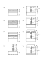
図1は、半導体装置100の断面図である。図1で例示するように、半導体装置100は、半導体基板10の主面上に、メサ20が設けられ、メサ20の両側面が埋込層30によって埋め込まれた構造を有する。半導体基板10の裏面には、裏面電極40が設けられている。埋込層30の上には、絶縁膜50がメサ20の上面を露出させるように設けられている。メサ20の上面から絶縁膜50の上面にかけて、上部電極60が設けられている。
FIG. 1 is a cross-sectional view of the
半導体基板10は、閃亜鉛鉱型の結晶構造を有するIII−V族化合物半導体であり、例えばInP基板である。半導体基板10は、一例としてn型の導電性を有するが、これに限定されるものではない。メサ20は、半導体基板10の主面上に設けられており、矢印Aの方向にストライプ状に設けられている。メサ20は、半導体基板10側から、バッファ層21、活性層22、回折格子層23、クラッド層24およびコンタクト層25が順に積層された構造を有する。なお、後述するが、回折格子層23とクラッド層24との間には、カバー層とスペーサ層とが設けられている。
The
バッファ層21は、一例としてn型のInPであり、例えば500nmの厚みを有する。ドーパントは、例えばSiである。活性層22は、光の生成に用いられる量子井戸発光層と、当該発光層への電子の注入に用いられる電子注入層とが交互かつ多段に積層されたカスケード構造を有する。具体的には、活性層22は、量子井戸発光層及び電子注入層からなる半導体積層構造を1周期分の単位積層体とし、この単位積層体が多段に積層されたカスケード構造を有する。量子井戸発光層及び電子注入層は、それぞれ、量子井戸層(GaInAs)及び量子障壁層(AlInAs)を含む所定の量子井戸構造を有している。それにより、単位積層体においては、量子井戸構造によるエネルギ準位構造であるサブバンド準位構造が形成される。活性層22は、一例として、半導体積層構造を30段有し、合計で約500層のGaInAs/AlInAsの多層構造を有し、例えば1.5μm程度の厚みを有する。
The
回折格子層23は、一例としてGaInAsであり、例えば500nm程度の厚みを有する。ここで、回折格子の結合定数κが小さすぎるとレーザ発振が起こらないおそれがある。一方、結合定数κが大きすぎると、ホールバーニング現象が起きてレーザ出力が緩和し、デバイス特性が悪化するおそれがある。そこで、結合定数κは、1〜3程度であることが好ましい。回折格子層23の凹凸のデューティ比、すなわち回折格子の周期に対する回折格子層の凸部の長さの割合を「a」とすると、結合定数κは近似的にsin(aπ)/πに比例するため、結合定数κはa=0.5の場合に最大となる。したがって、デューティ比aは、0.5に近いことが好ましい。a<0.2またはa>0.7の場合に、結合定数κは最大値の約1/2よりも小さくなる。以上のことから、デューティ比aは、0.2≦a≦0.7を満たすことが好ましい。また、結合定数κは、近似的に回折格子深さdに比例する。そこで、回折格子深さdは、75nm≦d≦500nmを満たすことが好ましい。ただし、結合定数κ=1〜3に対応させるためには、回折格子深さdは、75nm≦d≦225nmを満たすことが好ましい。
The
クラッド層24は、一例としてn型のInPであり、例えば2μmの厚みを有する。ドーパントは、例えばSiである。コンタクト層25は、一例としてGaInAsであり、例えば0.1μmの厚みを有する。埋込層30は、一例としてFeドープInPである。裏面電極40は、一例としてAuGeNi/Auである。絶縁膜50は、一例として酸化シリコン、窒化シリコンなどの絶縁体である。上部電極60は、一例としてTi/Pt/Auの3層構造の電極である。
The
次に、図2(a)〜図2(h)を参照しつつ、半導体装置100の製造方法について説明する。まず、半導体装置100の成長に用いる各種の半導体層の設定成長速度を測定する。設定成長速度とは、平坦な基板上に所定の条件で半導体層を成長させたときの、成長速度のことである。一例として、表面が平坦な半導体基板をOMVPE(Organo−Metallic Vapor Phase Epitaxy;有機金属気相成長)装置のリアクタにセットし、リアクタを所定の圧力まで減圧する。その後、PH3雰囲気下でリアクタを所定の温度に昇温し、所定の原料ガスをリアクタに供給して、所定の成長時間だけ半導体層を成長する。リアクタを室温まで降温して基板を取出し、成長した半導体層の一部をエッチングで除去して基板表面を露出させ、段差計を用いて半導体層の膜厚を測定する。この膜厚を成長時間で割った値を、設定成長速度とする。所定の圧力、温度、原料ガスの供給量および成長時間は、成長させようとする半導体層によって異なる。設定成長速度は、バッファ層21、活性層22、回折格子層23、カバー層72、スペーサ層73、クラッド層24およびコンタクト層について、事前に測定しておく。
Next, a method for manufacturing the
次に、一例として、半導体基板10をOMVPE装置のリアクタにセットし、リアクタを8000Pa(80mbar)程度まで減圧する。その後、PH3雰囲気下でリアクタを670℃(リアクタ設定温度)に昇温する。
Next, as an example, the
まず、図2(a)で例示するように、バッファ層21を、設定成長速度2.0μm/h、n型ドーパント=1×1017/cm3の成長条件で500nm成長させる。その後、リアクタを715℃に昇温してGaInAs/AlInAsからなる多層構造の活性層22(厚み1.5μm)を成長させる。GaInAs層のn型ドーパント濃度は、2×1017/cm3である。その後、回折格子層23を500nm成長させ、InPキャップ層を10nm成長させた後、PH3雰囲気で室温まで降温し、半導体基板10をOMVPE炉から取り出す。なお、図2(a)では、InPキャップ層の図示を省略している。
First, as illustrated in FIG. 2A, the
次に、図2(b)で例示するように、回折格子層23上のInPキャップ層上に、窒化シリコンなどのマスク71を所定の間隔を空けて形成する。なお、図2(b)は、図2(a)を90度回転させたものである。したがって、マスク71は、後の工程で形成されるメサストライプが延びる方向に所定の間隔を空けて複数配置されている。なお、メサストライプが延びる方向におけるマスク71の一つの長さは、例えば0.2μm〜1μm程度である。本実施形態においては、一例として、メサストライプが伸びる方向におけるマスク71の長さは0.6μmであり、マスク71同士の間隔も0.6μmである。
Next, as illustrated in FIG. 2B, a mask 71 made of silicon nitride or the like is formed on the InP cap layer on the
次に、マスク71をエッチングマスクとして用い、マスク71から露出している部分の回折格子層23をエッチングにより除去する。エッチングは、例えばハロゲン系ガスを用いたRIE(Reactive Ion Etching)により行う。それにより、回折格子層23に回折格子となる溝(凹部)が形成される。回折格子の周期は例えば1.2μmであり、デューティ比は例えば0.5であり、エッチングにより形成される凹部の深さは例えば450nmである。回折格子の周期及びデューティ比は、マスク71の長さ及び間隔を調整することによって変更可能である。その後、マスク71を除去する。
Next, using the mask 71 as an etching mask, the portion of the
次に、回折格子層23に対して、リン酸と過酸化水素水の混合液でウェットエッチングを行った後、半導体基板10を再度OMVPE装置のリアクタにセットし、リアクタを8000Pa(80mbar)程度まで減圧する。その後、PH3雰囲気下でリアクタを540℃に昇温する。540℃程度の低温のリアクタ内では、回折格子層23の凹凸の形状の変化や回折格子層23を構成する原子の抜けによる回折格子層23の組成変化を抑制することができる。その後、図3(a)で例示するように、回折格子層23上に、540℃でカバー層72を形成する。その後、670℃に昇温し、カバー層72上にスペーサ層73を順に形成する。
Next, after wet etching is performed on the
カバー層72は、一例としてn型InPである。ドーパントは、例えばSiである。カバー層72のドーパント濃度が高すぎると、デバイス特性が悪化するおそれがある。そこで、設定ドーパント濃度は、0/cm3<設定ドーパント濃度<5×1018/cm3とすることが好ましい。ここで設定ドーパント濃度とは、同じ成長条件下で基板の平坦な面上に成長した半導体層について、ホール測定で求めた半導体層のシート抵抗値を半導体層の厚さで除して算出する値のことである。本実施形態においては一例として2×1017/cm3である。回折格子の凹部において、カバー層72の層厚は、回折格子の凹部の深さより小さく、例えば回折格子の凹部の深さの1/3〜1/2程度であることが好ましい。ここで層厚とは、設定成長速度に成長時間を掛けた値のことである。カバー層の層厚が凹部深さの1/3より小さい場合、引き続いてスペーサ層を成長するために670℃まで昇温させた際に、薄いカバー層では、回折格子層からの原子の抜けや、原子のマストランスポート(回折格子を構成する原子が熱せられて表面を移動すること)による回折格子の変形を抑制できず、結果として引き続いて成長したスペーサ層の表面の凹凸が大きくなってしまい好ましくない。また、カバー層は比較的低温で成長するため結晶性が劣るが、カバー層の層厚が回折格子の凹部の深さの1/2よりも大きい場合、結晶性の悪いカバー層を厚く成長させることになり、この場合もやはり引き続いて成長するスペーサ層の表面に凸凹が生じてしまう。
The
本実施形態においては、カバー層72の層厚は、一例として200nmである。スペーサ層73は、一例としてn型InPである。ドーパントは、例えばSiである。設定ドーパント濃度は、例えば2×10¹⁷/cm3程度である。スペーサ層73の層厚は、例えば300nm程度である。スペーサ層73の少なくとも一部は、回折格子の凹部に形成されている。なお、カバー層72の設定ドーパント濃度とスペーサ層73の設定ドーパント濃度とは異なっていてもよい。
In the present embodiment, the
ここで、図3(b)で例示するように、回折格子の凹部を埋め込むようにカバー層72及びスペーサ層73を成長する際に、カバー層72の設定成長速度が比較的大きいと、回折格子の凸部上面における実際成長速度よりも凹部底面における実際成長速度が大きくなる傾向にある。なお、ここで実際成長速度とは、回折格子と同じ形状の凹凸上に成長した半導体層の厚さを、断面のSEM観察等によって測定して求められる値である。一定の時間間隔で組成の異なるマーカー層を挿入する成長を行うことで、凹部の底面上、凹部の側面上、凸部の上面上のそれぞれの成長速度を測定することができる。設定成長速度が大きいと、凸部上面の実際成長速度よりも凹部底面の実際成長速度が大きくなる傾向が見られる。この場合、凹部底面上の領域に含まれるドーパントの濃度が凸部上面上の領域に含まれるドーパントの濃度よりも小さくなる。それにより、キャリア濃度が不均一化し、十分に電流が注入されない領域と電流が集中する領域とが混在することになる。その結果、半導体装置100のレーザ特性が悪化するおそれがある。
Here, as illustrated in FIG. 3B, when the
そこで、本実施形態においては、カバー層72の設定成長速度を、スペーサ層73の設定成長速度よりも小さくする。すなわち、回折格子の凹部内において、底面に接するカバー層72(導電型の第1半導体層)の設定成長速度を、スペーサ層73(第2半導体層)の設定成長速度よりも小さくする。具体的には、カバー層の成長では、成長温度を低くし、リアクタへのIII族原料ガスの供給量を小さくする。カバー層72の設定成長速度が0.1μm/h以下、好ましくは0.06μm/h程度まで小さくなると、図3(a)で例示するように、成長モードが変化する。すなわち、マイグレーション(原料ガス中のIII族やV族の原子が表面を移動しながら堆積すること)が抑制される。すなわち、回折格子の凹部底面における実際成長速度と凸部上面における実際成長速度との差が小さくなる。それにより、凸部と凹部のドーパントの濃度の不均一化を抑制することができる。その結果、半導体装置100のレーザ特性の悪化を抑制することができる。なお、成長温度を低くするだけ、あるいは、III族(In)の供給量を減らすことだけによっても、成長速度を小さくすることができる。
Therefore, in this embodiment, the set growth rate of the
例えば、カバー層72の設定成長速度を0.1μm/h未満とすることが好ましい。また、カバー層72の設定成長速度をより小さくする観点から、カバー層72の設定成長速度を0.06μm/h以下とすることがより好ましい。また、カバー層72の設定成長速度を0.05μm以下とすることがより好ましい。カバー層72の成長過程においては、一例として、In(III族)原料の供給量を5.0×10−6mol/minとし、P(V族)原料の供給量を1.9×10−2mol/minとする。カバー層72の成長は、回折格子層の材料がGaInAsあるいはGaInAsPの場合には、リアクタの温度を520〜590℃の範囲にして行うのが好ましい。スペーサ層73の成長過程においては、一例として、In(III族)原料の供給量を3.2×10−5mol/minとし、P(V族)原料の供給量を0.9×10−2mol/minとし、リアクタの温度をカバー層の成長よりも上げて670℃で行う。
For example, the set growth rate of the
また、スペーサ層73の成長は、カバー層72側の部分(150nm)の成長速度を0.1μm/hとし、スペーサ層73の残りの部分(150nm)の成長速度を0.5μm/hとしてもよい。なお、スペーサ層73のカバー層72側の部分の成長を低温で行い、スペーサ層73の残りの部分の成長過程においては、リアクタ設定温度を670℃に昇温してもよい。
Further, the growth of the
図4は、回折格子層23上にカバー層72およびスペーサ層73を形成した実験例である。図4は、断面のSEM写真を模式的に描いたものである。回折格子層23の凹部深さを520nmとした。回折格子の周期を1.2μmとし、デューティ比を0.5とした。204nmのカバー層72の設定成長速度を0.06μm/hとし、スペーサ層73のカバー層72側部分(150nm)の設定成長速度を0.1μm/hとし、スペーサ層73のクラッド層24側部分(146nm)の設定成長速度を0.5μm/hとした。カバー層72およびスペーサ層73のカバー層72側部分の成長温度を540℃とし、スペーサ層73のクラッド層24側部分の成長温度を670℃とした。設定成長速度の変更は、原料供給量の変更及び温度の変更で行った。図4で例示するように、設定成長速度を段階的に上げることにより、回折格子の凹部底面における実際成長速度と凸部上面における実際成長速度との差がほとんど無くなったことが確認された。
FIG. 4 is an experimental example in which a
次に、図2(c)で例示するように、クラッド層24を、例えば、設定成長速度2.0μm/h、n型設定ドーパント濃度=8×1017/cm3の成長条件で2μm程度成長させる。成長時のリアクタの温度は670℃である。In(III族)原料の供給量を1.4×10−4mol/minとした。なお、図2(c)は、図2(a)と同じ方向の断面である。その後、670℃で、コンタクト層25を、例えば、設定成長速度2.0μm/h、n型設定ドーパント=1×1019/cm3の成長条件で計0.1μm程度成長させる。その後、PH3雰囲気で室温まで降温し、半導体基板10をリアクタから取り出す。
Next, as illustrated in FIG. 2C, the clad
次に、図2(d)で例示するように、メサ20を形成する領域上に、窒化シリコンなどのマスク74を形成する。次に、このマスク74をエッチングマスクとして用い、RIE装置などでドライエッチングを行う。それにより、[011]方向に延在するメサストライプを形成する。メサストライプの幅は、例えば5μm〜20μm程度である。また、メサ深さ(メサ20の高さ)は、6.0μm〜7.0μm程度である。
Next, as illustrated in FIG. 2D, a
その後、例えば、塩酸:酢酸:水:H2O2の混合溶液を用いてメサストライプの両側面を、0.25μm程度のウェットエッチングする。それにより、ドライエッチングによりメサ側面にできたダメージ層を除去する。さらに、HBr:水:Br2の混合溶液を用いてメサ側面の平滑化処理を行う。 Thereafter, for example, wet etching of about 0.25 μm is performed on both side surfaces of the mesa stripe using a mixed solution of hydrochloric acid: acetic acid: water: H 2 O 2 . Thereby, the damaged layer formed on the side surface of the mesa by dry etching is removed. Furthermore, HBr: Water: performing smoothing processing of the mesa side surface by using a mixed solution of Br 2.
次に、図2(e)で例示するように、メサ20の両側面に埋込層30を成長させる。一例として、図2(e)の埋込層30の成長工程においては、半導体基板10をリアクタにセットし、PH3雰囲気下で、成長温度:575℃、リアクタ圧力:10000Pa(100mbar)、Inの供給量:2.81×10⁻⁴mol/min、PH3の供給量:350sccm(1.56×10−2mol/min)、雰囲気中HCl濃度:11ppm、Cp2Fe流量:10sccm、埋め込み高さ:メサマスク+0.15μmの成長条件で、埋込層30をエピタキシャル成長させる。HClは埋込成長の開始時から供給し、埋込成長の間、HCl濃度は一定とする。その後、PH3雰囲気下で室温まで降温し、半導体基板10を取り出す。
Next, as illustrated in FIG. 2E, the buried layers 30 are grown on both side surfaces of the
次に、メサ20の上面および埋込層30の上面に、絶縁膜50を成膜する。次に、図2(f)で例示するように、メサ20の上面部分の絶縁膜50をエッチングなどで除去することによって、メサ20の上面を露出させる。その後、図2(g)で例示するように、メサ20の上面から絶縁膜50の上面にかけて、上部電極60を成膜する。次に、図2(h)で例示するように、半導体基板10の裏面を削ることによって半導体基板10を100μm程度まで薄膜化し、当該裏面に裏面電極40を成膜する。その後、エピウェハを分割することによってチップ化することによって、半導体装置100が完成する。
Next, an insulating
本実施形態に係る半導体装置の製造方法によれば、回折格子層23の回折格子上にカバー層72及びスペーサ層73を形成する際に、カバー層72の設定成長速度をスペーサ層73の設定成長速度よりも小さくすることによって、カバー層72におけるドーパントの濃度の不均一化を抑制することができる。また、カバー層72の設定成長速度を0.1μm/h未満とすることで、回折格子の凸部上と凹部上におけるカバー層72の実際成長速度の差を小さくすることができる。それにより、カバー層72におけるドーパントの濃度の不均一化を抑制することができる。
According to the manufacturing method of the semiconductor device according to the present embodiment, when the
10 半導体基板
20 メサ
21 バッファ層
22 活性層
23 回折格子層
24 クラッド層
25 コンタクト層
30 埋込層
40 裏面電極
50 絶縁膜
60 上部電極
71 マスク
72 カバー層
73 スペーサ層
74 マスク
100 半導体装置
DESCRIPTION OF
Claims (11)
前記回折格子層の凹凸上に、第1半導体層を形成する工程と、
前記第1半導体層上に第2半導体層を形成する工程と、を含み、
前記第1半導体層の設定成長速度を、前記第2半導体層の設定成長速度よりも小さくする、半導体装置の製造方法。 Forming a diffraction grating layer having irregularities on its surface on a semiconductor substrate;
Forming a first semiconductor layer on the irregularities of the diffraction grating layer;
Forming a second semiconductor layer on the first semiconductor layer,
A method for manufacturing a semiconductor device, wherein a set growth rate of the first semiconductor layer is made lower than a set growth rate of the second semiconductor layer.
前記回折格子層の凹凸上に、導電型の半導体層を形成する工程と、を含み、
前記半導体層の設定成長速度を、0.1μm/h未満にする、半導体装置の製造方法。 Forming a diffraction grating layer having irregularities on the surface on the active layer;
Forming a conductive semiconductor layer on the irregularities of the diffraction grating layer,
A method for manufacturing a semiconductor device, wherein the set growth rate of the semiconductor layer is less than 0.1 μm / h.
Priority Applications (1)
| Application Number | Priority Date | Filing Date | Title |
|---|---|---|---|
| JP2015104918A JP2016219667A (en) | 2015-05-22 | 2015-05-22 | Method of manufacturing semiconductor device |
Applications Claiming Priority (1)
| Application Number | Priority Date | Filing Date | Title |
|---|---|---|---|
| JP2015104918A JP2016219667A (en) | 2015-05-22 | 2015-05-22 | Method of manufacturing semiconductor device |
Publications (1)
| Publication Number | Publication Date |
|---|---|
| JP2016219667A true JP2016219667A (en) | 2016-12-22 |
Family
ID=57581528
Family Applications (1)
| Application Number | Title | Priority Date | Filing Date |
|---|---|---|---|
| JP2015104918A Pending JP2016219667A (en) | 2015-05-22 | 2015-05-22 | Method of manufacturing semiconductor device |
Country Status (1)
| Country | Link |
|---|---|
| JP (1) | JP2016219667A (en) |
Citations (4)
| Publication number | Priority date | Publication date | Assignee | Title |
|---|---|---|---|---|
| JPS61179525A (en) * | 1985-02-04 | 1986-08-12 | Agency Of Ind Science & Technol | Vapor growth method |
| JPH11330615A (en) * | 1998-05-13 | 1999-11-30 | Fujitsu Ltd | Manufacture of semiconductor device |
| JP2007042759A (en) * | 2005-08-01 | 2007-02-15 | Sumitomo Electric Ind Ltd | Method of manufacturing semiconductor light emitting device |
| US20110310915A1 (en) * | 2008-11-07 | 2011-12-22 | President And Fellows Of Harvard College | Methods and apparatus for single-mode selection in quantum cascade lasers |
-
2015
- 2015-05-22 JP JP2015104918A patent/JP2016219667A/en active Pending
Patent Citations (4)
| Publication number | Priority date | Publication date | Assignee | Title |
|---|---|---|---|---|
| JPS61179525A (en) * | 1985-02-04 | 1986-08-12 | Agency Of Ind Science & Technol | Vapor growth method |
| JPH11330615A (en) * | 1998-05-13 | 1999-11-30 | Fujitsu Ltd | Manufacture of semiconductor device |
| JP2007042759A (en) * | 2005-08-01 | 2007-02-15 | Sumitomo Electric Ind Ltd | Method of manufacturing semiconductor light emitting device |
| US20110310915A1 (en) * | 2008-11-07 | 2011-12-22 | President And Fellows Of Harvard College | Methods and apparatus for single-mode selection in quantum cascade lasers |
Similar Documents
| Publication | Publication Date | Title |
|---|---|---|
| JP6897928B2 (en) | Manufacturing method of optical semiconductor device and optical semiconductor device | |
| JP5545670B2 (en) | Optical semiconductor device and manufacturing method thereof | |
| KR960012356A (en) | A method of etching a semiconductor, a method of manufacturing a semiconductor device, and a method of manufacturing a semiconductor laser. And semiconductor lasers | |
| CN107528215B (en) | The manufacturing method of semiconductor element, semiconductor element | |
| JP2009252839A (en) | Semiconductor laser and manufacturing method therefor | |
| JP2015233093A (en) | Semiconductor device and method for manufacturing the same | |
| JP4772314B2 (en) | Nitride semiconductor device | |
| JP2007184491A (en) | Distributed feedback semiconductor laser | |
| JP2016219667A (en) | Method of manufacturing semiconductor device | |
| JP2006134926A5 (en) | ||
| JP2007042759A (en) | Method of manufacturing semiconductor light emitting device | |
| JP4762202B2 (en) | Semiconductor quantum dot device, manufacturing method thereof, optical switch, semiconductor laser, and photodetector | |
| JP6572640B2 (en) | Method for fabricating semiconductor light receiving element | |
| JP4853008B2 (en) | Method for fabricating a semiconductor optical device | |
| JP4985411B2 (en) | Method for fabricating a semiconductor optical device | |
| JP5531610B2 (en) | Manufacturing method of semiconductor laser device | |
| JP2008159684A (en) | Method for etching group iii nitride semiconductor | |
| JPH03250684A (en) | Manufacture of mesa buried type optical semiconductor device | |
| JP2008034531A (en) | Method of manufacturing compound semiconductor optical element | |
| US20070026550A1 (en) | Method of manufacturing semiconductor light emitting apparatus and semiconductor light emitting apparatus | |
| JP4121539B2 (en) | Manufacturing method of semiconductor device | |
| JP2010258273A (en) | Method of manufacturing semiconductor laser | |
| JP2018101752A (en) | Semiconductor optical element and method for manufacturing the same | |
| JPS5884483A (en) | Buried hetero-structure semiconductor laser | |
| JP2009260189A (en) | Method of manufacturing semiconductor light-emitting element |
Legal Events
| Date | Code | Title | Description |
|---|---|---|---|
| A621 | Written request for application examination |
Free format text: JAPANESE INTERMEDIATE CODE: A621 Effective date: 20180423 |
|
| A977 | Report on retrieval |
Free format text: JAPANESE INTERMEDIATE CODE: A971007 Effective date: 20190118 |
|
| A131 | Notification of reasons for refusal |
Free format text: JAPANESE INTERMEDIATE CODE: A131 Effective date: 20190129 |
|
| A02 | Decision of refusal |
Free format text: JAPANESE INTERMEDIATE CODE: A02 Effective date: 20190806 |