JP2016201545A - LED manufacturing method and LED - Google Patents
LED manufacturing method and LED Download PDFInfo
- Publication number
- JP2016201545A JP2016201545A JP2016112766A JP2016112766A JP2016201545A JP 2016201545 A JP2016201545 A JP 2016201545A JP 2016112766 A JP2016112766 A JP 2016112766A JP 2016112766 A JP2016112766 A JP 2016112766A JP 2016201545 A JP2016201545 A JP 2016201545A
- Authority
- JP
- Japan
- Prior art keywords
- led
- phosphor
- binder
- slurry
- filling
- Prior art date
- Legal status (The legal status is an assumption and is not a legal conclusion. Google has not performed a legal analysis and makes no representation as to the accuracy of the status listed.)
- Granted
Links
Images


Classifications
-
- H—ELECTRICITY
- H01—ELECTRIC ELEMENTS
- H01L—SEMICONDUCTOR DEVICES NOT COVERED BY CLASS H10
- H01L2224/00—Indexing scheme for arrangements for connecting or disconnecting semiconductor or solid-state bodies and methods related thereto as covered by H01L24/00
- H01L2224/01—Means for bonding being attached to, or being formed on, the surface to be connected, e.g. chip-to-package, die-attach, "first-level" interconnects; Manufacturing methods related thereto
- H01L2224/42—Wire connectors; Manufacturing methods related thereto
- H01L2224/47—Structure, shape, material or disposition of the wire connectors after the connecting process
- H01L2224/48—Structure, shape, material or disposition of the wire connectors after the connecting process of an individual wire connector
- H01L2224/4805—Shape
- H01L2224/4809—Loop shape
- H01L2224/48091—Arched
-
- H—ELECTRICITY
- H01—ELECTRIC ELEMENTS
- H01L—SEMICONDUCTOR DEVICES NOT COVERED BY CLASS H10
- H01L2224/00—Indexing scheme for arrangements for connecting or disconnecting semiconductor or solid-state bodies and methods related thereto as covered by H01L24/00
- H01L2224/80—Methods for connecting semiconductor or other solid state bodies using means for bonding being attached to, or being formed on, the surface to be connected
- H01L2224/85—Methods for connecting semiconductor or other solid state bodies using means for bonding being attached to, or being formed on, the surface to be connected using a wire connector
- H01L2224/85909—Post-treatment of the connector or wire bonding area
- H01L2224/8592—Applying permanent coating, e.g. protective coating
Landscapes
- Application Of Or Painting With Fluid Materials (AREA)
- Luminescent Compositions (AREA)
- Led Device Packages (AREA)
Abstract
Description
本発明はLEDに蛍光体を施与してLEDを製造する方法及び製造したLEDに関する。
特に、本発明は樹脂、溶液、蛍光体を含むスラーリーなどをLEDに充填または塗布し乾燥硬化する方法に係わり、さらには白色発光LEDを製造するための方法に係わる。
尚、本明細書中LED用部材とは完成品としてのLEDを製造する途中の中間部品としての部材等を意味しており、また本発明の塗布とは、連続的又は断続的なディスペンス、インクジェット、マイクロカーテン施与、スロットノズル施与、スクリーン印刷方式、霧化施与、静電霧化施与、スプレイ等を含むがこれらに限定するものではない。
The present invention relates to a method of manufacturing an LED by applying a phosphor to the LED and the manufactured LED.
In particular, the present invention relates to a method of filling or applying a resin, a solution, a slurry containing phosphor and the like to an LED and then drying and curing, and further relates to a method for manufacturing a white light emitting LED.
In the present specification, the LED member means a member or the like as an intermediate part in the process of manufacturing an LED as a finished product, and the application of the present invention means continuous or intermittent dispensing or inkjet. , Micro curtain application, slot nozzle application, screen printing method, atomization application, electrostatic atomization application, spray, and the like.
従来、白色発光LEDの製造方法として近紫外光や青色発光ダイオードにR(赤)、G(緑)、B(青)の蛍光体や少なくとも一つのYAG、TAG,シリカ(silica)系などの蛍光体、演色性をあげるためR、Gの蛍光体の組み合わせと2液反応熱硬化タイプシリコーンなどのバインダーを混合したスラーリー(slurry)をディスペンサー装置でディスペンス(dispense)したり、更に溶剤などを加えて粘度を低くし微粒子発生装置の一種であるスプレイ装置などを用いてLEDに直接スプレイ(spray)し被覆していた。 Conventionally, as a method for producing a white light emitting LED, near ultraviolet light, blue light emitting diodes, R (red), G (green), B (blue) phosphors and at least one YAG, TAG, silica (silica) based fluorescence Dispense slurry, which is a combination of R and G phosphors and binders such as two-component reactive thermosetting silicone, to increase body and color rendering, and dispense with solvent. The LED was directly sprayed and coated using a spray device, which is a kind of fine particle generator, with a reduced viscosity.
特許文献1は本出願人により提案されており、加熱したLEDチップ(chip)に蛍光体(phosphor)とバインダーと溶媒を含むスラーリーを圧縮エア(air)で粒子化させ薄膜でパルス的スプレイ流をもって積層塗布し、一般的なスプレイ方法ではコーティング(coating)することが難しいとされるLEDの側壁にも付着させてLEDを製造する方法が開示されている。 Patent Document 1 has been proposed by the present applicant, and a slurry containing phosphor, binder, and solvent is formed into particles with compressed air on a heated LED chip, and a pulsed spray flow is formed in a thin film. A method of manufacturing an LED by laminating and adhering to the side wall of the LED, which is difficult to coat by a general spraying method, is disclosed.
特許文献2にはLEDチップにシリコーン(silicon)などのバインダー(binder)を被覆し硬化させて、その上に蛍光体、バインダー、溶剤からなるスラーリー(slurry)を塗布し、必要により拡散材などをそれらに混合して積層する方法が提案されている。 In Patent Document 2, an LED chip is coated with a binder such as silicone and cured, and a slurry made of a phosphor, a binder and a solvent is applied thereon, and if necessary, a diffusion material or the like is applied. A method of laminating them by mixing them has been proposed.
非特許文献1などに開示されているようなディスペンサー(dispenser)を用いる方法はハイパワー(high power)でない砲弾型LEDやバックライト(back light)向けなどのカップ(cup)の内側に装着されたチップに前記スラーリーを充填して大量生産向けに多く採用されている。 A method using a dispenser as disclosed in Non-Patent Document 1 is mounted inside a cup such as a bullet-type LED that is not high power or a backlight (back light). Many of these chips are used for mass production by filling the slurry.
特許文献1の方法ではパルス的にインパクトをもってスラーリーを塗布できるのでLEDチップの側壁もコーティングでき、また薄膜で多層に塗布するのでLEDチップのエッジカバーもよく、塗着効率も極めて高くできるが、セラミックスなどのLED基板に組み込まれたLEDチップとLEDチップの間まで塗布するか、不必要な個所はマスクをして塗布するので蛍光体の使用効率は低かった。特にLEDチップ間の距離が離れている基板の場合は極めて効率が悪かった。 In the method of Patent Document 1, slurries can be applied with impact in a pulse manner, so that the side walls of LED chips can also be coated, and since the thin film is applied in multiple layers, the edge cover of the LED chips is good and the coating efficiency can be extremely high. The application efficiency of the phosphor was low because it was applied to the space between the LED chip and the LED chip incorporated into the LED substrate, or unnecessary portions were applied as a mask. In particular, in the case of a substrate in which the distance between the LED chips is large, the efficiency is extremely poor.
特許文献2ではバインダーをLEDチップに被覆し硬化させた後、その上に蛍光体を含むスラーリーをエアスプレイ方法で塗布する方法が開示されているが、通常のエアスプレイを使用する方法は塗着効率が極めて悪いことが業界の常識である。 Patent Document 2 discloses a method in which a binder is coated on an LED chip and cured, and then a slurry containing phosphor is coated thereon by an air spray method. However, a method using a normal air spray is a coating method. It is common knowledge in the industry that efficiency is extremely poor.
一方、非特許文献1などに開示されるような簡易装置を使用して無溶剤のシリコーンなどのバインダーと蛍光体からなるスラーリーをディスペンサーなどで塗布する場合はマスキングを必要とせず生産性も高いが、図7に示すようにLEDチップの中央が盛り上がり、端部が薄くなって垂直光のみならず空間分布も悪く、ハイパワーの照明用としては不向きであった。
また仮にリフレクターをダム替わりにするなどしてスラーリーを充填しても膜厚が厚いため乱反射等で光のロスが生じ蛍光体効率のロスにつながっていた。
On the other hand, when a slurry made of a binder such as solventless silicone and a phosphor is applied with a dispenser using a simple device as disclosed in Non-Patent Document 1 or the like, masking is not required and productivity is high. As shown in FIG. 7, the center of the LED chip swells, the end becomes thin, and not only vertical light but also the spatial distribution is bad, which is unsuitable for high power illumination.
Moreover, even if the slurry was filled by replacing the reflector with a dam, the film thickness was too thick, resulting in loss of light due to irregular reflection or the like, leading to loss of phosphor efficiency.
一方LED用に特化したスクリーン印刷法ではバインダーのシリコーン樹脂などは2液硬化タイプを使用するのでポットライフの関係で長時間使用できず、しかしコーティング品質を安定させるために大量にスラーリーを作成する必要があったため、ポットライフを過ぎたスラーリーは大量に廃棄していたため使用効率は極めて低かった。
蛍光体膜を均一に形成できるUS6576488B2の電気泳動方式は理想的であったがプロセスが複雑で業界では敬遠されがちであった。
LEDチップに可能な限り薄く均一に蛍光体膜を形成させ、蛍光体の使用効率を上げることが業界では求められていた。
On the other hand, in the screen printing method specialized for LED, the silicone resin of the binder uses a two-component curing type, so it cannot be used for a long time due to pot life, but a large amount of slurry is created to stabilize the coating quality. Because it was necessary, the slurries past the pot life were discarded in large quantities, so the usage efficiency was extremely low.
The electrophoretic method of US6576488B2 that can form a phosphor film uniformly was ideal, but the process was complicated and it was apt to be avoided in the industry.
There has been a need in the industry to form a phosphor film as thinly and uniformly as possible on an LED chip to increase the usage efficiency of the phosphor.
本発明は前述の課題を解決するためになされたもので、本発明の目的は性能が一般的な工法より遥かに優れ蛍光体の使用効率の高いLED製造方法を提供することである。 The present invention has been made to solve the above-described problems, and an object of the present invention is to provide an LED manufacturing method that has far superior performance than a general construction method and high use efficiency of a phosphor.
本発明は複数のLEDが配置された基板のLEDに少なくとも第1の蛍光体とバインダーからなり、その重量比率が0.01:1乃至1:1の第1のスラーリーを少なくとも1層塗布または充填する第一の工程と、次いで少なくともLED部が開口されたマスクを前記基板上にセットする第二の工程と、第2の蛍光体と溶媒のみのスラーリー又は第2の蛍光体とバインダーの重量比が1:0.01乃至1:0.5の混合体と溶媒からなるスラーリーを少なくとも前記LED開口部に少なくとも1層塗布または充填する第三の工程からなり、マスク上に付着した第2の蛍光体又は第2の蛍光体とバインダー混合体を回収することを特徴とするLEDの製造方法を提供する。 In the present invention, at least one layer of a first slurry having a weight ratio of 0.01: 1 to 1: 1 is applied to or filled in an LED on a substrate on which a plurality of LEDs are arranged, comprising at least a first phosphor and a binder. A first step, a second step of setting a mask having at least an LED portion opened on the substrate, and a second phosphor and a solvent-only slurry or a weight ratio of the second phosphor and the binder. Is a third step of applying or filling at least one layer of slurry comprising a mixture of 1: 0.01 to 1: 0.5 and a solvent into the LED opening, and the second fluorescence deposited on the mask. A method for producing an LED is provided, wherein the body or the second phosphor and the binder mixture are recovered.
更に本発明は前記複数のLEDが配置された基板がウェハーレベルLEDまたはセラミック基板LEDであってLED部を開口したマスクを前記基板にセットする第一の工程と、第1の蛍光体とバインダーの重量比が0.01:1乃至1:1の混合体からなる第1のスラーリーを少なくともLEDの周囲に充填する第二の工程と、第2の蛍光体と溶媒とからなるスラーリーまたは第2の蛍光体とバインダーとの重量比が1:0.01乃至1:0.5の混合体と溶媒とからなる第2のスラーリーをLEDに少なくとも1層充填または塗布する第三の工程とからなりマスク上に付着した第2の蛍光体または第2の蛍光体とバインダーの混合体を回収することを特徴とするLEDの製造方法を提供する。 Furthermore, the present invention provides a first step in which the substrate on which the plurality of LEDs are arranged is a wafer level LED or a ceramic substrate LED, and a mask having an LED portion opened is set on the substrate, and the first phosphor and binder A second step of filling at least the periphery of the LED with a first slurry comprising a mixture having a weight ratio of 0.01: 1 to 1: 1; and a slurry or second comprising a second phosphor and a solvent. A mask comprising a third step of filling or coating at least one layer of a second slurry comprising a mixture of a phosphor and a binder in a weight ratio of 1: 0.01 to 1: 0.5 and a solvent. Provided is a method for manufacturing an LED, wherein the second phosphor or the mixture of the second phosphor and a binder adhering to the upper phosphor is collected.
本発明はまた、ウェハーレベルLEDまたはセラミック基板LEDのLED部を開口した第1のマスクを前記基板にセットする第一の工程と、第1の蛍光体とバインダーの重量比が0.01:1乃至1:1の混合体からなる第1のスラーリーを少なくともLEDの周囲に充填する第二の工程と、前記第1のマスクの替わりにまたは第1のマスクの上から第2のマスクをセットする第三の工程と、第2の蛍光体と溶媒とからなるスラーリーまたは第2の蛍光体とバインダーとの重量比が1:0.01乃至1:0.5の混合体と溶媒とからなる第2のスラーリーを少なくとも1層塗布する第四の工程とからなり第2のマスク上に付着した第2の蛍光体または第2の蛍光体とバインダーの混合体を回収することを特徴とするLEDの製造方法を提供する。 The present invention also provides a first step of setting a first mask having an LED portion of a wafer level LED or a ceramic substrate LED on the substrate, and the weight ratio of the first phosphor to the binder is 0.01: 1. A second step of filling at least the periphery of the LED with a first slurry consisting of a 1: 1 mixture, and setting a second mask instead of the first mask or over the first mask. A third step and a slurry comprising a second phosphor and a solvent, or a mixture comprising a mixture and a solvent having a weight ratio of the second phosphor to the binder of 1: 0.01 to 1: 0.5. And a fourth step of applying at least one layer of slurry of 2 and collecting the second phosphor or the mixture of the second phosphor and the binder adhering to the second mask. A manufacturing method is provided.
前記本発明のLEDの製造方法において、前記少なくとも第2の蛍光体を含むスラーリーの塗布はスプレイ、または微粒子発生装置で発生させた微粒子で塗布することが好ましい。 In the method for producing an LED of the present invention, it is preferable that the slurry containing at least the second phosphor is applied by spraying or fine particles generated by a fine particle generator.
また前記本発明のLEDの製造方法において、前記スプレイまたは微粒子塗布が5乃至200Hzのパルス的に行われることが好ましい。 In the LED manufacturing method of the present invention, it is preferable that the spraying or fine particle coating is performed in a pulsed manner of 5 to 200 Hz.
また前記本発明のLEDの製造方法において、前記第1の蛍光体及び第2の蛍光体は同一種類であることが好ましい。 In the LED manufacturing method of the present invention, it is preferable that the first phosphor and the second phosphor are of the same type.
本発明は、LEDが青色発光LEDであって前記第2の蛍光体は赤、緑、黄色から選択された少なくとも2種類の蛍光体を積層するに当たりマスクはそれぞれの蛍光体の種類に対応して用意されることを特徴とするLEDの製造方法を提供する。 In the present invention, when the LED is a blue light emitting LED and the second phosphor is laminated with at least two kinds of phosphors selected from red, green, and yellow, the mask corresponds to the type of each phosphor. An LED manufacturing method is provided.
また本発明では、LEDが近紫外光LEDであって、第1の蛍光体は青、緑、赤の蛍光体の混色であって、第2の蛍光体は青、緑、赤を積層するにあたりマスクはそれぞれの蛍光体の種類に対応して用意されることを特徴とするLEDの製造方法を提供する。 In the present invention, the LED is a near-ultraviolet LED, the first phosphor is a mixed color of blue, green, and red phosphors, and the second phosphor is used for stacking blue, green, and red. Provided is a method for manufacturing an LED, wherein a mask is prepared corresponding to each phosphor type.
更に本発明では、前記マスクを取り外し少なくとも第2の蛍光体を含むスラーリーの層の上からバインダーを塗布することを特徴とするLEDの製造方法を提供する。 Furthermore, the present invention provides a method for producing an LED, wherein the mask is removed and a binder is applied from above the slurry layer containing at least the second phosphor.
本発明では回収した蛍光体または蛍光体とバインダーの混合体を溶媒で希釈してスラーリーとしマスクを用いて前記塗布または充填方法で製造されたLEDを提供する。 The present invention provides an LED manufactured by the coating or filling method using a mask by diluting a collected phosphor or a mixture of the phosphor and a binder with a solvent to form a slurry.
本発明の製造方法によれば第1の蛍光体とバインダーの混合体層はバインダーリッチであるので最終工程のレンズモールドでの密着性も問題ない。 According to the production method of the present invention, since the first phosphor and binder mixture layer is rich in binder, there is no problem in adhesion with the lens mold in the final process.
また最初の層の第1の蛍光体とバインダーの混合体には溶媒を加えて流動性を上げ、所望する箇所に容易に充填を行うことができる。そうすることによりパルス的スプレイなどの塗布も容易に行うことができる。 In addition, a solvent can be added to the first phosphor and binder mixture in the first layer to increase fluidity, and the desired portion can be easily filled. By doing so, application such as pulse spraying can be easily performed.
特にリードフレームタイプLEDにはリフレクターが形成されているので充填する場合あえてダムを形成する必要がなく、マスクも必要としないため生産性を上げることができる。
第1のスラーリーの充填レベルをLEDの上面プラスマイナス30ミクロン以内とし第2の蛍光体スラーリーまたは蛍光体リッチのスラーリーを薄膜で充填すれば性能のみならず生産性は飛躍的に向上する。
当然このやり方はセラミック基板タイプLEDやCOB(チップオンボード)、などにも応用でき充填したい箇所にダムを作成したり、充填したい部分が開口されたマスクを基板にセットして蛍光体を充填できる。COBの場合は第1の蛍光体からなるスラーリーを充填しバインダーの硬化を促進させたのち個々のLEDに対応したマスクをセットして第2の蛍光体からなるスラーリーを充填または塗布することできる。
In particular, since the lead frame type LED is formed with a reflector, it is not necessary to form a dam when filling, and a mask is not required, so that productivity can be increased.
If the filling level of the first slurry is within the upper surface of the LED plus or minus 30 microns and the second phosphor slurry or phosphor rich slurry is filled with a thin film, not only the performance but also the productivity is dramatically improved.
Naturally, this method can also be applied to ceramic substrate type LEDs and COB (Chip On Board), etc., and can be used to create dams at locations where filling is desired, or to set a mask with an opening where filling is desired on the substrate and fill with phosphors . In the case of COB, after filling the slurry made of the first phosphor to promote the curing of the binder, a mask corresponding to each LED can be set and the slurry made of the second phosphor can be filled or applied.
充填はポッティングでも良いが、エアスプレイやエアアシストスプレイのエア圧と流量を低くして充填してもよい。充填はパルス的でも良い。例えばエア圧は5乃至100KPaで流量は1乃至20NL/min.で良い。そうすることによってスラーリーが粗い粒子で付着するので飛び散りを抑えることができる。 The filling may be potting, but the filling may be performed by lowering the air pressure and flow rate of the air spray or air assist spray. The filling may be pulsed. For example, the air pressure is 5 to 100 KPa and the flow rate is 1 to 20 NL / min. Good. By doing so, slurries adhere with coarse particles, so that scattering can be suppressed.
前記リフレクターに蛍光体を付着させずにスプレイ塗布したい場合はリフレクターをカバーするような立体的なマスクを設置すべきである。
第1のスラーリーの充填層や塗布層の上から第2の蛍光体を含むスラーリーをパルス的スプレイにインパクトを与えることによって又はジェット流に乗せて移送することもできるのでバインダーリッチの層に蛍光体を潜り込むように付着させることができる。
When spray coating is desired without attaching the phosphor to the reflector, a three-dimensional mask that covers the reflector should be installed.
The slurry containing the second phosphor can be transported by impacting the pulsed spray or on the jet stream from above the first slurry filling layer or coating layer, so that the phosphor can be transferred to the binder-rich layer. Can be attached to sink.
更に本発明では蛍光体を溶媒に分散させてスラーリーを作成する際の溶媒または分散媒はエタノールなどのマイルドなアルコール系溶剤や水あるいはそれらの混合体、更には液化炭酸ガスなどの液化ガスなどを使用できる。これらの方法でシリコーンなどのバインダーを含む蛍光体層の上に積層する場合、溶媒や分散媒はシリコーンに対する溶解性に乏しいので溶媒を95%以上揮発させと塗布時パウダー状にして塗布することが望ましい。 Furthermore, in the present invention, the solvent or dispersion medium for producing the slurry by dispersing the phosphor in the solvent is a mild alcohol solvent such as ethanol, water or a mixture thereof, and further a liquefied gas such as liquefied carbon dioxide gas. Can be used. When laminating on a phosphor layer containing a binder such as silicone by these methods, the solvent or dispersion medium is poorly soluble in silicone. desirable.
上記のように本発明によれば例えば第1の蛍光体とバインダーからなる蛍光体を含むスラーリーをLEDの周りに充填する際、蛍光体量は側壁から出る光を所望する色温度に変換できるようしたら良く、スラーリーの充填をLED上面ギリギリのレベルか少し覆うぐらいにするとLEDのエッジのカバーは無視できる。LEDをスラーリーで充填し覆う場合はLED表面をフレーム(炎)、コロナ、プラズマ処理などで濡れを向上させておくことが好ましい。 As described above, according to the present invention, for example, when a slurry including a phosphor made of the first phosphor and a binder is filled around the LED, the amount of the phosphor can convert the light emitted from the side wall to a desired color temperature. Once you have filled the slurry to the level of the top surface of the LED or just to cover it a little, you can ignore the LED edge cover. When the LED is filled with a slurry and covered, it is preferable to improve the wettability of the LED surface with a frame (flame), corona, plasma treatment or the like.
このような方法を採用することによりインパクトをもったパルス的スプレイと同じ効果を得ることができるうえに、高価な蛍光体を容易に回収できるので、付加価値の高い高品質なLEDが低コストで製造できる。 By adopting such a method, it is possible to obtain the same effect as a pulsed spray with impact, and it is possible to easily collect expensive phosphors, so that high-value LEDs with high added value can be obtained at low cost. Can be manufactured.
以下、図面を参照して本発明の好適な実施形態について説明する。なお、以下の実施形態は発明の理解を容易にするための一例にすぎず本発明の技術的思想を逸脱しない範囲において当業者により実施可能な付加、置換、変形等を施すことを排除するものではない。 Hereinafter, preferred embodiments of the present invention will be described with reference to the drawings. The following embodiments are merely examples for facilitating understanding of the invention, and exclude additions, substitutions, modifications, etc. that can be implemented by those skilled in the art without departing from the technical idea of the present invention. is not.
図面は本発明の好適な実施の形態を概略的に示している。 The drawings schematically show a preferred embodiment of the invention.
図1においてLEDはスラーリーをパルス的スプレイ流にインパクトを与えながら薄膜で積層することによって、より具体的には本出願人が権利を有する特願2011−200395の方法や装置を使用して行うことにより側面も被覆でき塗着効率は95%以上が可能であり好適な塗膜形成を行うことができる。
しかし不必要な個所まで塗布するので蛍光体の使用効率が極めて悪かった。基板上のLED間のピッチが広いと蛍光体の実際の使用効率は5%に満たないことさえあった。
In FIG. 1, an LED is formed by laminating slurries with a thin film while impacting a pulsed spray flow, more specifically, using the method and apparatus of Japanese Patent Application No. 2011-200395 to which the present applicant has the right. Thus, the side surface can also be coated, and the coating efficiency can be 95% or more, and a suitable coating film can be formed.
However, the use efficiency of the phosphor was extremely poor because it was applied to unnecessary parts. When the pitch between the LEDs on the substrate was wide, the actual usage efficiency of the phosphor was even less than 5%.
また性能を上げるためには薄膜が求められ蛍光体の比率をバインダーより多くする必要があり、蛍光体が多すぎると樹脂のレンズモールディングングの際に基板との密着性が悪くなるため一般的にはマスクをしてコートしない個所を残す必要であった。 In order to improve performance, a thin film is required, and the ratio of the phosphor is required to be larger than that of the binder. If too much phosphor is used, the adhesion to the substrate is deteriorated during resin lens molding. Needed to leave a mask and not coat.
図2以降に示す本発明の形態の第1変形例においては図1に示すLEDなどと対応する部分については図1の参照番号に順次10,20,30,40,50,60をプラスして表記し以下には図1との相違を主として説明する。 In the first modification of the embodiment of the present invention shown in FIG. 2 and subsequent figures, the portions corresponding to the LEDs shown in FIG. 1 are sequentially added with 10, 20, 30, 40, 50, 60 to the reference numbers in FIG. The difference from FIG. 1 will be mainly described below.
図2においてLEDチップ11やワイヤー12に干渉しないようにマスク14をセットする。そしてマスク開口からバインダーリッチのスラーリーを充填又は塗布し、また必要によりバインダーの硬化を促進させた後その上に第2の蛍光体からなるスラーリーを充填又は塗布する。前記バインダーまたは第1の蛍光体とバインダーの混合体は充填などをしやすくまた気泡が混入しにくいように溶解性のある溶媒で希釈したほうが好ましい。
In FIG. 2, the
充填方法を採用する場合、事前にLEDの濡れ性を良くするためプラズマなどで表面処理を行うことが好ましいし、事前に被充填部に溶媒を施与すると尚良い。
またより蛍光体を均一に塗布させるために第1蛍光体を含むスラーリーも第2の蛍光体を含むスラーリーも複数回に分けて充填又は塗布を行うことが肝要である。第1の蛍光体を含むスラーリーを充填する場合の乾燥硬化したスラーリーの充填レベルはLEDの高さの±30マイクロメートル以内にした方がエッジカバーを良くしトータル膜厚を少なくすることができ、空間的色温度を調整しやすくできるので好ましい。
When the filling method is adopted, it is preferable to perform surface treatment with plasma or the like in advance in order to improve the wettability of the LED, and it is more preferable to apply a solvent to the filling portion in advance.
In order to more uniformly apply the phosphor, it is important to fill or apply the slurry including the first phosphor and the slurry including the second phosphor in a plurality of times. When filling the slurry containing the first phosphor, the dry and cured slurryy filling level should be within ± 30 micrometers of the LED height to improve the edge cover and reduce the total film thickness. This is preferable because the spatial color temperature can be easily adjusted.
また充填後の蛍光体の沈降を防ぎたい場合は、基板は加熱すべきであり、いずれの混合体やスラーリーも充填又は塗布を行う都度バインダーの硬化は促進たさせた方が好ましいし、充填または塗布後蛍光体を沈降させたい場合は溶媒を含むスラーリーにして粘度をさげることができる。 In addition, in order to prevent sedimentation of the phosphor after filling, the substrate should be heated, and it is preferable to accelerate the curing of the binder every time any mixture or slurry is filled or applied. When it is desired to precipitate the phosphor after coating, the viscosity can be reduced by making a slurry containing a solvent.
図3においてLED又はそれを含む基板等はバインダーと第1の蛍光体を含む混合体でコーティングされる。混合体には溶媒や拡散材を加えても良い。塗布装置は問わないがインパクトを付加したパルス的スプレイが好適である。
基板全体をコーティングする場合は後工程のレンズモールド樹脂の密着性を考慮すると蛍光体の含有量は重量比で50%以下が好ましく、理想的には3乃至30%以下が好ましい。理由はバインダーのみより蛍光体が存在するとチクソトロピック性が向上し側壁の垂れやエッジの引けが起こりにくいからである。また蛍光体の含有量はLEDの側面から発光する量と体積当たりの色変換により決定すべきである。またマスクをセットする際は指触乾燥程度にバインダーの乾燥または硬化を促進させることが好ましい。
In FIG. 3, an LED or a substrate including the LED is coated with a mixture including a binder and a first phosphor. A solvent or a diffusing material may be added to the mixture. Although a coating apparatus is not ask | required, the pulsed spray which added the impact is suitable.
In the case of coating the entire substrate, the phosphor content is preferably 50% or less by weight, and ideally 3 to 30% or less, considering the adhesion of the lens mold resin in the subsequent process. The reason is that if a phosphor is present rather than only a binder, thixotropic properties are improved and side wall dripping and edge shrinkage are unlikely to occur. The phosphor content should be determined by the amount of light emitted from the side of the LED and the color conversion per volume. Moreover, when setting a mask, it is preferable to accelerate | stimulate drying or hardening of a binder to the extent of finger touch drying.
第2の蛍光体とバインダーを含むスラーリーを充填する際はマスクを密着したほうが良いが、低温で硬化が促進するバインダーを使用する場合であってスプレイ塗布する際はマスクを基板より少し浮かせた方がマスク上のバインダーの硬化のスピードを抑えられるので回収の面からは都合がよい。通常LEDは吸着加熱テーブルで吸着して熱伝導をさせるので、断熱性のマスクを採用したりマスクへの吸着力を弱めるなどして行うと良い。充填または塗布後はすばやくマスクを除去し基板を吸着させて50乃至120℃に加熱したテーブルまたは遠赤外線ヒーターなどで硬化を急速に促進させることができる。 When filling the slurry containing the second phosphor and binder, it is better to adhere the mask, but when using a binder that promotes curing at low temperatures, the mask is slightly lifted from the substrate when spray coating is applied. However, since the speed of curing of the binder on the mask can be suppressed, it is convenient from the viewpoint of recovery. Usually, LEDs are adsorbed by an adsorption heating table to conduct heat, so it is preferable to employ a heat-insulating mask or weaken the adsorption force to the mask. After filling or coating, the mask can be quickly removed, the substrate can be adsorbed, and curing can be accelerated rapidly by a table or far infrared heater heated to 50 to 120 ° C.
図4においてLED31の周辺、または必要によりLED上部まで充填され
た第1の蛍光体を含むスラーリーの塗布層の少なくとも一部とLEDの上部に第2のスラーリーを塗布器でスプレイ塗布し蛍光体層35を形成させる。塗布器はトラバースしながら蛍光体の分散を考慮して薄膜で3乃至15層スプレイ塗布したほうがより均一に蛍光体が分散できるので性能は向上する。LEDの色温度分布を理想的なものにするためにLEDの上部にマスク34をセットしマスク開口部と塗布領域はLEDの構造、LED周囲または上部の蛍光体の比率などにより決定すべきである。
またフィリップチップタイプを除きマスクの位置はワイヤー32より高い位置にセットすることによりハンドリングが容易になるため自動化が図れる。
In FIG. 4, the second slurry is spray-coated with an applicator at least a part of the slurry coating layer including the first phosphor filled around the
Further, except for the Philip chip type, the mask position is set higher than the
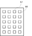
図5はマスク44でLEDチップやワイヤーが干渉しないように開口が形成してある。
In FIG. 5, the
図6は本発明により形成された塗膜である。バインダーと第1の蛍光体を含むスラーリー層53は複数層でよくまた第2の蛍光体を含むスラーリー層55も複数層にした方が好ましい。バインダーが実質的に0の第2蛍光体のみのスラーリーの塗布後は振動等で蛍光体が離脱しないようにバインダーのみで薄膜でカバーコート層55の形成もできる。もちろんのこと基板全体を例えば5マイクロメートル以下にコートすることもできる。
FIG. 6 is a coating film formed according to the present invention. The
図7は従来のディスペンサーなどにおけるLED61に蛍光体が含まれるスラーリーを塗布した略図で中央部の膜厚が厚くエッジ(edge)がカバー(cover)できないので色温度にバラツキが生じる。又塗布量が少ないとリード線62が接合されるパッド付近は陰になり塗布されにくい。
FIG. 7 is a schematic diagram in which a slurry including phosphor is applied to the
図8、図9はバインダーまたはバインダーリッチ層78に第2の蛍光体または第2の蛍光体とバインダーからなる粒子79がスプレイ流またはジェット流で衝突し潜り込むイメージを表している。
FIG. 8 and FIG. 9 show an image in which the second phosphor or the
従来技術では、例えば平均粒度分布が8マイクロメートル前後で1マイクロメートル以下から30マイクロメートルの分布をしている比重の高い蛍光体と、比重の比較的低いバインダーと、必要により加えた溶媒とからなるスラーリーを単位面積当たり±1.5%のバラツキをもって一回で薄膜塗布するのは至難の業であった。理由はミクロ的に見たら粒子の大きい部位と小さい部位は当然存在するからである。 In the prior art, for example, a phosphor having a high specific gravity having an average particle size distribution of about 8 micrometers and a distribution of 1 micrometer or less to 30 micrometers, a binder having a relatively low specific gravity, and a solvent added if necessary. It was extremely difficult to apply the slurry with a thin film at a time with a variation of ± 1.5% per unit area. The reason is that, when viewed microscopically, there are naturally large portions and small portions of particles.
本発明では特願2011−200395の技術を応用し第1のバインダーまたはスラーリーや第2の蛍光体を含むスラーリーの分散を良好に保ちながら塗布できる。さらに2つのシリンジ間に塗布機を設け、両方のシリンジ内のスラーリーを撹拌装置で撹拌しながら2つのシリンジ内のスラーリーを差圧で移動させることができる。特に蛍光体と溶媒のみ、あるいは蛍光体とバインダーの重量比が1:0.5乃至1:0.01の溶媒を含むスラーリー、複数種の蛍光体と溶媒からなるスラーリーの沈降防止と分散安定性にメリットが有る。またこの方式では沈降を防止できるので差圧を低くでき単位時間当たりの塗布量を絞ることもができるメリットもある。シリンジ容積を大きく例えば150ml以上にする場合は複数の羽根を設置し、上昇、下降の撹拌流を発生させることもできる。 In the present invention, the technique of Japanese Patent Application No. 2011-200395 is applied, and coating can be performed while maintaining good dispersion of the first binder or slurry containing the slurry or the second phosphor. Furthermore, an applicator is provided between the two syringes, and the slurry in the two syringes can be moved with a differential pressure while stirring the slurry in both syringes with a stirring device. In particular, slurries containing only a phosphor and a solvent, or a solvent having a phosphor / binder weight ratio of 1: 0.5 to 1: 0.01, and slurries composed of a plurality of types of phosphors and solvents are prevented from sedimentation and dispersion stability. There are merits. Further, this method has an advantage that the settling can be prevented, so that the differential pressure can be lowered and the coating amount per unit time can be reduced. When the syringe volume is increased to, for example, 150 ml or more, a plurality of blades can be installed to generate an ascending and descending stirring flow.
本発明を使用して薄膜で5層以上を積層することにより粒度分布の悪い蛍光体を使用しても確率の面からも塗布膜を均一にすることができる。
更に循環回路の好ましい部位に超音波等の振動を付加することにより更に良好な分散状態を保つことができる。また好適な塗膜形成ではLEDの表面を電気泳動と同じく導電性を持たせることにより、例えばスプレイ塗布の場合、霧化された粒子を静電気などで帯電させることにより静電反発で霧化粒子同士の凝集を防ぎ微粒子も付着させることができるので理想的な蛍光体塗布ができ理想的なLEDを製造できる。
By laminating five or more thin films using the present invention, even if a phosphor having a poor particle size distribution is used, the coating film can be made uniform in terms of probability.
Furthermore, by adding vibrations such as ultrasonic waves to a preferable portion of the circulation circuit, a better dispersion state can be maintained. Further, in the case of forming a suitable coating film, the surface of the LED is made conductive as in electrophoresis. For example, in the case of spray coating, the atomized particles are electrostatically repelled by charging the atomized particles with static electricity or the like. Therefore, it is possible to apply an ideal phosphor and to manufacture an ideal LED.
また本発明は、一種類のスラーリーを単一の塗布器で多層に塗布することに限定するものでなく、複数の塗布器で複数の蛍光体を多層塗布することも出来る。すなわち、本発明によれば、複数の塗布ブースに複数の塗布器を設置するだけでなく、1つの塗装ブース内に複数の塗布器を設置した塗布装置を用い、種類の異なる複数の蛍光体をLEDに積層し乾燥させてLEDを製造することができる。前記少なくとも2種類の蛍光体の積層は少なくとも赤色、緑色、黄色、青色の蛍光体から選択することが出来る。 In addition, the present invention is not limited to applying a single type of slurry to multiple layers with a single applicator, and multiple phosphors can be applied in multiple layers with multiple applicators. That is, according to the present invention, not only installing a plurality of applicators in a plurality of coating booths, but also using a coating apparatus in which a plurality of applicators are installed in a single coating booth, The LED can be manufactured by laminating and drying the LED. The laminate of the at least two kinds of phosphors can be selected from at least red, green, yellow, and blue phosphors.
また、前記少なくとも第2の蛍光体を含むスラーリーの蛍光体は少なくともバインダーを実質的に0にまた可能な限りバインダーを少なくするようにしたスラーリーとすると回収し蛍光体の再利用の面で好適である。 In addition, the slurry phosphor containing at least the second phosphor is preferably a slurry that is at least substantially free of binder and less binder as much as possible, and is suitable in terms of recovery and reuse of the phosphor. is there.
蛍光体の回収に適してさえいればマスクの寸法や形状、材質は問わないが、高性能のまま蛍光体を回収し再利用する場合は蛍光体で研磨されにくいセラミックス系材質が理想であり表面仕上げがよいほどバインダーが混入していても超音波洗浄機などを用いて短時間で除去し回収できる。 The size, shape, and material of the mask are not limited as long as it is suitable for the recovery of the phosphor, but when collecting and reusing the phosphor with high performance, a ceramic material that is difficult to be polished by the phosphor is ideal and the surface Even if the binder is mixed so that the finish is good, it can be removed and collected in a short time using an ultrasonic cleaner or the like.
またマスクはコンタミネーションの面からもLED表面や蛍光体に使用される材質と同じか影響を与えない例えばセラミックや金属に無機系の材料をコーティングするなどした方が好ましい。
高速生産向けには、例えばフッ素系やポリイミドアミド樹脂に代表されるような耐熱、耐溶剤性のプラスチックフィルムの裏面にシ予めリコーン系、架橋したアクリル系、ウレタン系等の耐熱、耐溶剤性の粘着剤を施して予めLED基板にラミネートすることもできる。
Further, it is preferable that the mask has the same or no influence on the surface of the LED or the phosphor from the viewpoint of contamination, for example, a ceramic or metal is coated with an inorganic material.
For high-speed production, heat and solvent resistant such as ricone, cross-linked acrylic and urethane on the back of heat and solvent resistant plastic films such as fluorine and polyimideamide resin. An adhesive can be applied and laminated on the LED substrate in advance.
塗布器がエアスプレイあるいはエアアシストスプレイあるいは特に第2蛍光体からなるスラーリーを粒子製造装置で粒子化した後ジェット流で蛍光体粒子を搬送する場合、LED基板表面でのそれらのパターン幅は1乃至20mm程度になるようにすることが好ましい。
パターン幅はチップの形状や種類によりチップ全体の所望するそれぞれの部位の膜厚を考慮して選択すべきである。
When the applicator transports phosphor particles by jet flow after the sprayer is made into air spray, air-assisted spray, or particularly slurry made of the second phosphor by the particle production apparatus, the pattern width on the surface of the LED substrate is 1 to It is preferable to be about 20 mm.
The pattern width should be selected in consideration of the film thickness of each desired portion of the entire chip depending on the shape and type of the chip.
スプレイする場合などフロー性やバインダーの硬化を促進させることや、スプレイなどの塗膜形成時に発生する気化熱による温度低下などを考慮してLEDを30乃至120℃の範囲に加温し、LEDとスプレイヘッドとの距離を5乃至90mmに設定し、LEDに到達する際のスプレイパターン幅を1乃至20mmとし、スプレイエア圧を0.1乃至0.4MPaでパルス的に噴出させ、パルス的にインパクトを与えながらスプレイすることが好適である。 Heating the LED in the range of 30 to 120 ° C. in consideration of the flowability and curing of the binder such as when spraying, and the temperature decrease due to the heat of vaporization generated when forming a coating film such as spray, The distance from the spray head is set to 5 to 90 mm, the spray pattern width when reaching the LED is set to 1 to 20 mm, the spray air pressure is jetted in a pulse of 0.1 to 0.4 MPa, and the pulse is impacted. It is preferable to spray while giving
単色或いは複数色に関わらず特に第2蛍光体を含むスラーリーは層ごとに或いは所望する層ごとに塗膜重量を自動的に測定し精査しながら塗布または充填することが好ましく、特に最終層の一つ前の層で色温度を測定し、必要により塗布量を補正しながら所望する品質にすることが肝要である。 Regardless of the single color or multiple colors, slurries including the second phosphor are preferably applied or filled while automatically measuring and examining the coating weight for each layer or for each desired layer. It is important to measure the color temperature in the previous layer and to obtain the desired quality while correcting the coating amount if necessary.
本発明によれば特に付加価値の高いLEDを高品位に保ちながら高価な蛍光体を回収して再利用するので、従来プロセスより使用効率を10倍以上も高くできることから、大幅なコスト低減ができる。 According to the present invention, since expensive phosphors are collected and reused while keeping high value-added LEDs in high quality, the usage efficiency can be increased by 10 times or more compared to the conventional process, so that the cost can be greatly reduced. .
1,11,21,31,41,51,61,71 LED
2,12,22,32,42,52,62 ワイヤー
3,63 蛍光体層
13,23,33,43,53 第1の蛍光体層
14,34,44 マスク
15,25,35,55 第2の蛍光体層
56 バインダー(カバー層)
78 第1の蛍光体
79 第2の蛍光体
1,11,21,31,41,51,61,71 LED
2, 12, 22, 32, 42, 52, 62
78
Claims (14)
Priority Applications (1)
| Application Number | Priority Date | Filing Date | Title |
|---|---|---|---|
| JP2016112766A JP6507434B2 (en) | 2016-06-06 | 2016-06-06 | LED manufacturing method and LED |
Applications Claiming Priority (1)
| Application Number | Priority Date | Filing Date | Title |
|---|---|---|---|
| JP2016112766A JP6507434B2 (en) | 2016-06-06 | 2016-06-06 | LED manufacturing method and LED |
Related Parent Applications (1)
| Application Number | Title | Priority Date | Filing Date |
|---|---|---|---|
| JP2014142443A Division JP2016018960A (en) | 2014-07-10 | 2014-07-10 | Manufacturing method of led and led |
Publications (2)
| Publication Number | Publication Date |
|---|---|
| JP2016201545A true JP2016201545A (en) | 2016-12-01 |
| JP6507434B2 JP6507434B2 (en) | 2019-05-08 |
Family
ID=57422765
Family Applications (1)
| Application Number | Title | Priority Date | Filing Date |
|---|---|---|---|
| JP2016112766A Active JP6507434B2 (en) | 2016-06-06 | 2016-06-06 | LED manufacturing method and LED |
Country Status (1)
| Country | Link |
|---|---|
| JP (1) | JP6507434B2 (en) |
Citations (4)
| Publication number | Priority date | Publication date | Assignee | Title |
|---|---|---|---|---|
| JP2004111882A (en) * | 2002-09-20 | 2004-04-08 | Toyoda Gosei Co Ltd | Light emitting apparatus |
| JP2012248553A (en) * | 2011-05-25 | 2012-12-13 | Panasonic Corp | Light-emitting device and luminaire using the same |
| WO2013038953A1 (en) * | 2011-09-14 | 2013-03-21 | エムテックスマート株式会社 | Led manufacturing method, led manufacturing device, and led |
| WO2014103671A1 (en) * | 2012-12-28 | 2014-07-03 | シャープ株式会社 | Light emitting device |
-
2016
- 2016-06-06 JP JP2016112766A patent/JP6507434B2/en active Active
Patent Citations (4)
| Publication number | Priority date | Publication date | Assignee | Title |
|---|---|---|---|---|
| JP2004111882A (en) * | 2002-09-20 | 2004-04-08 | Toyoda Gosei Co Ltd | Light emitting apparatus |
| JP2012248553A (en) * | 2011-05-25 | 2012-12-13 | Panasonic Corp | Light-emitting device and luminaire using the same |
| WO2013038953A1 (en) * | 2011-09-14 | 2013-03-21 | エムテックスマート株式会社 | Led manufacturing method, led manufacturing device, and led |
| WO2014103671A1 (en) * | 2012-12-28 | 2014-07-03 | シャープ株式会社 | Light emitting device |
Also Published As
| Publication number | Publication date |
|---|---|
| JP6507434B2 (en) | 2019-05-08 |
Similar Documents
| Publication | Publication Date | Title |
|---|---|---|
| JP6211420B2 (en) | LED manufacturing method, LED manufacturing apparatus, and LED | |
| WO2016006120A1 (en) | Led manufacturing method and led | |
| EP2543060B1 (en) | Methods for application of optical materials to optical elements | |
| US9608174B2 (en) | Coating method and device | |
| CN103429949B (en) | The method that reflectance coating is provided for the substrate for luminescent device | |
| JP6033413B2 (en) | Method for producing optoelectronic elements and apparatus for producing optoelectronic elements | |
| JP2015217360A (en) | Film forming device of phosphor layer and film forming method of phosphor layer | |
| US20170136492A1 (en) | Method of applying powder or granular material | |
| WO2015121794A1 (en) | Systems and methods for application of coatings including thixotropic agents onto optical elements, and optical elements having coatings including thixotropic agents | |
| JP6233872B2 (en) | LED manufacturing method | |
| CN102120213B (en) | LED fluorescent powder spraying process | |
| JP2016201545A (en) | LED manufacturing method and LED | |
| KR20130051207A (en) | Method for manufacturing light emitting device package | |
| TWI537058B (en) | LED light fluorescent powder ultrasonic spraying process | |
| US20120313120A1 (en) | Method For Depositing A Phosphor Layer On LEDs, And Apparatus Made Thereby | |
| TW201143155A (en) | Method of manufacturing LED device | |
| CN210535692U (en) | Quantum dot packaging film | |
| CN110665769B (en) | Spraying method, spraying equipment and sprayed product obtained by adopting spraying method | |
| TWI610467B (en) | Wavelength conversion film, manufacturing method thereof and light-emitting device using the same | |
| TWI645584B (en) | Wavelength conversion film, manufacturing method thereof and light-emitting device using the same | |
| CN104347778A (en) | Fluorescent powder coating method, and LED (Light Emitting Diode) lamp and support thereof | |
| JP2016221518A (en) | Conductive film formation device and method of the same | |
| JP2016190380A (en) | Method for manufacturing three-dimensional molded object, apparatus for manufacturing three-dimensional molded object, and three-dimensional molded object | |
| KR20160137815A (en) | Method for Forming Light Blocking Layer of LED Chip |
Legal Events
| Date | Code | Title | Description |
|---|---|---|---|
| A621 | Written request for application examination |
Free format text: JAPANESE INTERMEDIATE CODE: A621 Effective date: 20170615 |
|
| A977 | Report on retrieval |
Free format text: JAPANESE INTERMEDIATE CODE: A971007 Effective date: 20180221 |
|
| A131 | Notification of reasons for refusal |
Free format text: JAPANESE INTERMEDIATE CODE: A131 Effective date: 20180327 |
|
| A521 | Request for written amendment filed |
Free format text: JAPANESE INTERMEDIATE CODE: A523 Effective date: 20180614 |
|
| A131 | Notification of reasons for refusal |
Free format text: JAPANESE INTERMEDIATE CODE: A131 Effective date: 20180920 |
|
| A521 | Request for written amendment filed |
Free format text: JAPANESE INTERMEDIATE CODE: A523 Effective date: 20181116 |
|
| TRDD | Decision of grant or rejection written | ||
| A01 | Written decision to grant a patent or to grant a registration (utility model) |
Free format text: JAPANESE INTERMEDIATE CODE: A01 Effective date: 20190314 |
|
| A61 | First payment of annual fees (during grant procedure) |
Free format text: JAPANESE INTERMEDIATE CODE: A61 Effective date: 20190314 |
|
| R150 | Certificate of patent or registration of utility model |
Ref document number: 6507434 Country of ref document: JP Free format text: JAPANESE INTERMEDIATE CODE: R150 |
|
| R250 | Receipt of annual fees |
Free format text: JAPANESE INTERMEDIATE CODE: R250 |