JP2016181663A - Multilayer capacitor - Google Patents
Multilayer capacitor Download PDFInfo
- Publication number
- JP2016181663A JP2016181663A JP2015062562A JP2015062562A JP2016181663A JP 2016181663 A JP2016181663 A JP 2016181663A JP 2015062562 A JP2015062562 A JP 2015062562A JP 2015062562 A JP2015062562 A JP 2015062562A JP 2016181663 A JP2016181663 A JP 2016181663A
- Authority
- JP
- Japan
- Prior art keywords
- electrode
- element body
- arithmetic average
- average roughness
- pair
- Prior art date
- Legal status (The legal status is an assumption and is not a legal conclusion. Google has not performed a legal analysis and makes no representation as to the accuracy of the status listed.)
- Pending
Links
Images
Classifications
-
- H—ELECTRICITY
- H01—ELECTRIC ELEMENTS
- H01G—CAPACITORS; CAPACITORS, RECTIFIERS, DETECTORS, SWITCHING DEVICES, LIGHT-SENSITIVE OR TEMPERATURE-SENSITIVE DEVICES OF THE ELECTROLYTIC TYPE
- H01G4/00—Fixed capacitors; Processes of their manufacture
- H01G4/30—Stacked capacitors
-
- H—ELECTRICITY
- H01—ELECTRIC ELEMENTS
- H01G—CAPACITORS; CAPACITORS, RECTIFIERS, DETECTORS, SWITCHING DEVICES, LIGHT-SENSITIVE OR TEMPERATURE-SENSITIVE DEVICES OF THE ELECTROLYTIC TYPE
- H01G4/00—Fixed capacitors; Processes of their manufacture
- H01G4/002—Details
- H01G4/228—Terminals
- H01G4/232—Terminals electrically connecting two or more layers of a stacked or rolled capacitor
-
- H—ELECTRICITY
- H01—ELECTRIC ELEMENTS
- H01G—CAPACITORS; CAPACITORS, RECTIFIERS, DETECTORS, SWITCHING DEVICES, LIGHT-SENSITIVE OR TEMPERATURE-SENSITIVE DEVICES OF THE ELECTROLYTIC TYPE
- H01G4/00—Fixed capacitors; Processes of their manufacture
- H01G4/002—Details
- H01G4/018—Dielectrics
- H01G4/06—Solid dielectrics
- H01G4/08—Inorganic dielectrics
- H01G4/12—Ceramic dielectrics
Landscapes
- Engineering & Computer Science (AREA)
- Power Engineering (AREA)
- Manufacturing & Machinery (AREA)
- Microelectronics & Electronic Packaging (AREA)
- Chemical & Material Sciences (AREA)
- Fixed Capacitors And Capacitor Manufacturing Machines (AREA)
- Ceramic Engineering (AREA)
- Inorganic Chemistry (AREA)
- Ceramic Capacitors (AREA)
Abstract
Description
本発明は、積層コンデンサに関する。 The present invention relates to a multilayer capacitor.
直方体形状を呈しており、第一方向で互いに対向している一対の主面と、一対の主面を連結するように第一方向に延びていると共に第一方向と直交する第二方向で互いに対向している一対の第一側面と、一対の主面を連結するように第一方向に延びていると共に第一及び第二方向に直交する第三方向で互いに対向している一対の第二側面と、を有している素体と、第一方向で互いに対向するように素体内に交互に配置されている複数の内部電極と、素体の一対の第二側面側にそれぞれ配置されていると共に複数の内部電極のうち対応する内部電極に接続されている一対の端子電極と、を備えている積層コンデンサが知られている(たとえば、特許文献1参照)。 It has a rectangular parallelepiped shape and extends in the first direction so as to connect the pair of main surfaces facing each other in the first direction and in the second direction orthogonal to the first direction. A pair of second side surfaces that extend in the first direction so as to connect the pair of opposed first side surfaces and the pair of main surfaces and face each other in a third direction orthogonal to the first and second directions A plurality of internal electrodes alternately disposed in the element body so as to face each other in the first direction, and a pair of second side surfaces of the element body, respectively. In addition, a multilayer capacitor is known that includes a pair of terminal electrodes connected to a corresponding internal electrode among a plurality of internal electrodes (see, for example, Patent Document 1).
近年、情報端末機器などの電子機器では、小型化及び薄型化が進んでいる。それに伴って、電子機器に搭載される基板や基板に搭載される電子部品においても、小型化が進んでおり、高密度実装化も進んでいる。更なる小型化を図るために、基板内に電子部品が埋め込まれている、電子部品内蔵基板も開発されてきている。電子部品内蔵基板では、基板の内部に電子部品が埋め込まれて実装されている。基板に形成された配線と埋め込まれている電子部品とは、確実に、電気的に接続される必要がある。しかしながら、特許文献1に記載された積層コンデンサでは、基板への埋め込み(基板への内蔵)、及び、基板に形成された配線との電気的な接続については考慮されていない。 In recent years, electronic devices such as information terminal devices have been reduced in size and thickness. Along with this, miniaturization is progressing in boards mounted on electronic devices and electronic components mounted on boards, and high-density mounting is also progressing. In order to further reduce the size, electronic component-embedded substrates in which electronic components are embedded in the substrate have been developed. In the electronic component built-in substrate, the electronic component is embedded and mounted inside the substrate. The wiring formed on the substrate and the embedded electronic component must be reliably electrically connected. However, in the multilayer capacitor described in Patent Document 1, no consideration is given to embedding in a substrate (incorporation into the substrate) and electrical connection with wiring formed on the substrate.
本発明は、低背化が図られ、基板に形成される配線との接続性を確保しつつ、基板に適切に内蔵することが可能な積層コンデンサを提供することを目的とする。 It is an object of the present invention to provide a multilayer capacitor that can be appropriately built in a substrate while ensuring a low profile and ensuring connectivity with wiring formed on the substrate.
本発明に係る積層コンデンサは、直方体形状を呈しており、互いに対向している一対の主面と、一対の主面を連結するように一対の主面が対向している方向に延びている四つの側面と、を有している素体と、一対の主面が対向している方向で互いに対向するように素体内に交互に配置されている複数の内部電極と、素体の互いに対向する一対の側面側にそれぞれ配置されていると共に複数の内部電極のうち対応する内部電極に接続されている一対の端子電極と、を備え、一対の主面が対向している方向での素体の長さは、一対の側面が対向している方向での素体の長さ及び一対の側面とは別の一対の側面が対向している方向での素体の長さよりも小さく、各端子電極は、主面に配置されている第一電極部分と、側面に配置されている第二電極部分とを有し、第一電極部分の表面の算術平均粗さが、0.20〜0.26μmであり、第二電極部分の表面の算術平均粗さが、0.27〜0.38μmである。 The multilayer capacitor according to the present invention has a rectangular parallelepiped shape, and extends in a direction in which the pair of principal surfaces face each other so as to connect the pair of principal surfaces to each other and the pair of principal surfaces. And a plurality of internal electrodes arranged alternately in the element body so as to face each other in a direction in which the pair of main surfaces face each other, and the element bodies face each other. A pair of terminal electrodes disposed on a pair of side surfaces and connected to a corresponding internal electrode among the plurality of internal electrodes, and the element body in a direction in which the pair of main surfaces face each other The length is smaller than the length of the element body in the direction in which the pair of side surfaces face each other and the length of the element body in the direction in which the pair of side surfaces different from the pair of side surfaces face each other. Are the first electrode part arranged on the main surface and the second electrode arranged on the side surface The arithmetic average roughness of the surface of the first electrode portion is 0.20 to 0.26 μm, and the arithmetic average roughness of the surface of the second electrode portion is 0.27 to 0.38 μm. is there.
本発明に係る積層コンデンサでは、一対の主面が対向している方向での素体の長さが、一対の側面が対向している方向での素体の長さ及び一対の側面とは別の一対の側面が対向している方向での素体の長さよりも小さい。これにより、積層コンデンサの低背化が図られ、基板への内蔵に適した積層コンデンサを実現することができる。各端子電極は、主面に配置されている第一電極部分を有している。したがって、本発明に係る積層コンデンサは、主面側において、基板に形成された配線と電気的に接続可能となり、基板への内蔵が容易である。 In the multilayer capacitor according to the present invention, the length of the element body in the direction in which the pair of main surfaces face each other is different from the length of the element body in the direction in which the pair of side surfaces face each other and the pair of side surfaces. Smaller than the length of the element body in the direction in which the pair of side surfaces face each other. As a result, the multilayer capacitor can be reduced in height, and a multilayer capacitor suitable for incorporation in a substrate can be realized. Each terminal electrode has a first electrode portion disposed on the main surface. Therefore, the multilayer capacitor according to the present invention can be electrically connected to the wiring formed on the substrate on the main surface side, and can be easily embedded in the substrate.
積層コンデンサは、基板の収容部に配置された後に、収容部に樹脂が充填されることにより、基板に内蔵される。積層コンデンサが基板に内蔵された後に、各端子電極(第一電極部分)に到達するビアホールが基板に形成され、ビアホール内に導体が形成される。ビアホール内に形成された導体と第一電極部分とが接続される。 After the multilayer capacitor is disposed in the housing portion of the substrate, the housing portion is filled with a resin, thereby being built in the substrate. After the multilayer capacitor is built in the substrate, a via hole reaching each terminal electrode (first electrode portion) is formed in the substrate, and a conductor is formed in the via hole. A conductor formed in the via hole is connected to the first electrode portion.
本発明に係る積層コンデンサでは、第一電極部分の表面の算術平均粗さが、0.20〜0.26μmであり、第二電極部分の表面の算術平均粗さが、0.27〜0.38μmである。このため、ビアホール内に形成された導体と第一電極部分との間と、収容部に充填された樹脂と第二電極部分との間とに、空隙が発生するのを防ぐことができると共に、上記導体と第一電極部分との剥離と、上記樹脂と第二電極部分との剥離とが生じるのを防ぐことができる。これにより、基板に形成される配線との接続性を確保しつつ、積層コンデンサの基板への内蔵を適切に行うことができる。 In the multilayer capacitor according to the present invention, the arithmetic average roughness of the surface of the first electrode portion is 0.20 to 0.26 μm, and the arithmetic average roughness of the surface of the second electrode portion is 0.27 to 0. 38 μm. For this reason, it is possible to prevent the occurrence of voids between the conductor formed in the via hole and the first electrode portion, and between the resin filled in the housing portion and the second electrode portion, It is possible to prevent the peeling between the conductor and the first electrode portion and the peeling between the resin and the second electrode portion. Accordingly, the multilayer capacitor can be appropriately embedded in the substrate while ensuring connectivity with the wiring formed on the substrate.
素体における一対の端子電極から露出している部分の表面の算術平均粗さが、0.14〜0.19μmであってもよい。この場合、収容部に充填された樹脂と素体との間に空隙が発生するのを防ぐことができると共に、上記樹脂と素体との剥離が生じるのを防ぐことができる。これにより、積層コンデンサの基板への内蔵をより一層適切に行うことができる。 The arithmetic mean roughness of the surface of the portion exposed from the pair of terminal electrodes in the element body may be 0.14 to 0.19 μm. In this case, it is possible to prevent a gap from being generated between the resin filled in the accommodating portion and the element body, and to prevent the resin from being separated from the element body. As a result, the multilayer capacitor can be more appropriately incorporated into the substrate.
本発明によれば、低背化が図られ、基板に形成される配線との接続性を確保しつつ、基板に適切に内蔵することが可能な積層コンデンサを提供することができる。 According to the present invention, it is possible to provide a multilayer capacitor that can be reduced in height and can be appropriately embedded in a substrate while ensuring connectivity with wiring formed on the substrate.
以下、添付図面を参照して、本発明の実施形態について詳細に説明する。なお、説明において、同一要素又は同一機能を有する要素には、同一符号を用いることとし、重複する説明は省略する。 Hereinafter, embodiments of the present invention will be described in detail with reference to the accompanying drawings. In the description, the same reference numerals are used for the same elements or elements having the same function, and redundant description is omitted.
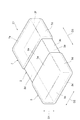
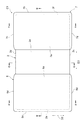
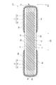
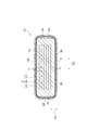
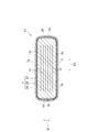
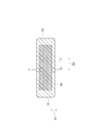
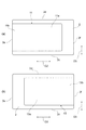
図1〜図6を参照して、本実施形態に係る積層コンデンサC1の構成を説明する。図1は、本実施形態に係る積層コンデンサを示す斜視図である。図2は、本実施形態に係る積層コンデンサを示す平面図である。図3は、図2におけるIII−III線に沿った断面構成を説明するための図である。図4は、図2におけるIV−IV線に沿った断面構成を説明するための図である。図5は、図2におけるV−V線に沿った断面構成を説明するための図である。図6は、図2におけるVI−VI線に沿った断面構成を説明するための図である。 With reference to FIGS. 1-6, the structure of the multilayer capacitor C1 which concerns on this embodiment is demonstrated. FIG. 1 is a perspective view showing the multilayer capacitor in accordance with this embodiment. FIG. 2 is a plan view showing the multilayer capacitor according to the present embodiment. FIG. 3 is a diagram for explaining a cross-sectional configuration along the line III-III in FIG. 2. FIG. 4 is a diagram for explaining a cross-sectional configuration along the line IV-IV in FIG. FIG. 5 is a diagram for explaining a cross-sectional configuration along the line V-V in FIG. 2. FIG. 6 is a diagram for explaining a cross-sectional configuration along the line VI-VI in FIG. 2.
積層コンデンサC1は、図1〜図6に示されるように、直方体形状を呈している素体2と、素体2の外表面に配置される第一端子電極5及び第二端子電極7と、を備えている。第一端子電極5と第二端子電極7とは、離間している。直方体形状には、角部及び稜線部が面取りされている直方体の形状、及び、角部及び稜線部が丸められている直方体の形状が含まれる。
As shown in FIGS. 1 to 6, the multilayer capacitor C <b> 1 includes an
素体2は、その外表面として、互いに対向している略長方形状の一対の主面2a,2bと、互いに対向している一対の第一側面2c,2dと、互いに対向している一対の第二側面2e,2fと、を有している。一対の主面2a,2bが対向している方向が第一方向D1であり、一対の第一側面2c,2dが対向している方向が第二方向D2であり、一対の第二側面2e,2fが対向している方向が第三方向D3である。本実施形態では、第一方向D1は、素体2の高さ方向である。第二方向D2は、素体2の幅方向であり、第一方向D1と直交している。第三方向D3は、素体2の長手方向であり、第一方向D1と第二方向D2とに直交している。
The
素体2の第一方向D1の長さは、素体2の第三方向D3の長さ及び素体2の第二方向D2の長さよりも小さい。素体2の第三方向D3の長さは、素体2の第二方向D2の長さよりも大きい。素体2の第三方向D3の長さは、たとえば、0.4〜1.6mmに設定される。素体2の第二方向D2の長さは、たとえば、0.2〜0.8mmに設定される。素体2の第一方向D1の長さは、たとえば、0.1〜0.35mmに設定される。積層コンデンサC1は、超低背型の積層コンデンサである。素体2の第二方向D2の長さは、素体2の第三方向D3の長さと同等であってもよく、また、素体2の第二方向D2の長さが、素体2の第三方向D3の長さよりも大きくてもよい。
The length of the
同等とは、等しいことに加えて、予め設定した範囲での微差又は製造誤差などを含んだ値を同等としてもよい。たとえば、複数の値が、当該複数の値の平均値の±5%の範囲内に含まれているのであれば、当該複数の値は同等であると規定する。 “Equivalent” may be equivalent to a value including a slight difference or a manufacturing error in a preset range in addition to being equal. For example, if a plurality of values are included in a range of ± 5% of the average value of the plurality of values, the plurality of values are defined to be equivalent.
一対の第一側面2c,2dは、主面2aと主面2bとの間を連結するように第一方向D1に延びている。一対の第一側面2c,2dは、第三方向D3(一対の主面2a,2bの長辺方向)にも延びている。一対の第二側面2e,2fは、主面2aと主面2bとの間を連結するように第一方向D1に延びている。一対の第二側面2e,2fは、第二方向D2(一対の主面2a,2bの短辺方向)にも延びている。
The pair of first side surfaces 2c, 2d extends in the first direction D1 so as to connect the
素体2は、主面2aと主面2bとが対向している方向(第一方向D1)に複数の誘電体層が積層されて構成されている。素体2では、複数の誘電体層の積層方向(以下、単に「積層方向」と称する。)が第一方向D1と一致する。各誘電体層は、例えば誘電体材料(BaTiO3系、Ba(Ti,Zr)O3系、又は(Ba,Ca)TiO3系などの誘電体セラミック)を含むセラミックグリーンシート(以下、単に「グリーンシート」と称する。)の焼結体から構成される。実際の素体2では、各誘電体層は、各誘電体層の間の境界が視認できない程度に一体化されている。
The
積層コンデンサC1は、図3〜図6に示されるように、複数の第一内部電極11と、複数の第二内部電極13と、を備えている。第一及び第二内部電極11,13は、積層型の電気素子の内部電極として通常用いられる導電性材料(たとえば、Ni又はCuなど)からなる。第一及び第二内部電極11,13は、上記導電性材料を含む導電性ペーストの焼結体として構成される。
As illustrated in FIGS. 3 to 6, the multilayer capacitor C <b> 1 includes a plurality of first
第一内部電極11と第二内部電極13とは、第一方向D1において異なる位置(層)に配置されている。すなわち、第一内部電極11と第二内部電極13とは、素体2内において、第一方向D1に間隔を有して対向するように交互に配置されている。第一内部電極11と第二内部電極13とは、互いに極性が異なる。
The first
各第一内部電極11は、図7の(a)に示されるように、主電極部11aと、接続部11bと、を含んでいる。接続部11bは、主電極部11aの一辺(一方の短辺)から延び、第一側面2cに露出している。第一内部電極11は、第二側面2eに露出し、一対の主面2a,2b、一対の第一側面2c,2d、及び第二側面2fには露出していない。主電極部11aと、接続部11bとは、一体的に形成されている。
As shown in FIG. 7A, each first
主電極部11aは、第三方向D3を長辺方向とし、第二方向D2を短辺方向とする矩形形状を呈している。すなわち、各第一内部電極11の主電極部11aは、第三方向D3の長さが第二方向D2の長さよりも大きい。接続部11bは、主電極部11aの第二側面2e側の端部から第二側面2eまで延びている。接続部11bの第三方向D3の長さは、主電極部11aの第三方向D3の長さよりも小さい。接続部11bの第二方向D2の長さは、主電極部11aの第二方向D2の長さと同等である。接続部11bは、第二側面2eに露出した端部で、第一端子電極5に接続されている。接続部11bの第二方向D2の長さは、主電極部11aの第二方向D2の長さよりも小さくてもよい。
The
各第二内部電極13は、図7の(b)に示されるように、主電極部13aと、接続部13bと、を含んでいる。主電極部13aは、第一方向D1で素体2の一部(誘電体層)を介して主電極部11aと対向している。接続部13bは、主電極部13aの一辺(一方の短辺)から延び、第二側面2fに露出している。第二内部電極13は、第二側面2fに露出し、一対の主面2a,2b、一対の第一側面2c,2d、及び第二側面2eには露出していない。主電極部13aと、接続部13bとは、一体的に形成されている。
Each 2nd
主電極部13aは、第三方向D3を長辺方向とし、第二方向D2を短辺方向とする矩形形状を呈している。すなわち、各第二内部電極13の主電極部13aは、第三方向D3の長さが第二方向D2の長さよりも大きい。接続部13bは、主電極部13aの第二側面2f側の端部から第二側面2fまで延びている。接続部13bの第三方向D3の長さは、主電極部13aの第三方向D3の長さよりも小さい。接続部13bの第二方向D2の長さは、主電極部13aの第二方向D2の長さと同等である。接続部13bは、第二側面2fに露出した端部で、第二端子電極7に接続されている。接続部13bの第二方向D2の長さは、主電極部13aの第二方向D2の長さよりも小さくてもよい。
The
第一端子電極5は、第三方向D3に見て、素体2における第二側面2e側の端部に位置している。第一端子電極5は、主面2aに配置されている電極部分5a、主面2bに配置されている電極部分5b、第二側面2eに配置されている電極部分5c、及び、一対の第一側面2c,2dに配置されている電極部分5dを有している。すなわち、第一端子電極5は、五つの面2a,2b,2c,2d,2eに形成されている。互いに隣り合う電極部分5a,5b,5c,5d同士は、素体2の稜線部において接続されており、電気的に接続されている。
The first
電極部分5aと電極部分5cとは、主面2aと第二側面2eとの間の稜線部において、接続されている。電極部分5aと電極部分5dとは、主面2aと各第一側面2c,2dとの間の稜線部において、接続されている。電極部分5bと電極部分5cとは、主面2bと第二側面2eとの間の稜線部において、接続されている。電極部分5bと電極部分5dとは、主面2bと各第一側面2c,2dとの間の稜線部において、接続されている。電極部分5cと電極部分5dとは、第二側面2eと各第一側面2c,2dとの間の稜線部において、接続されている。
The
電極部分5cは、各接続部11bの第二側面2eに露出した部分をすべて覆うように配置されており、接続部11bは、第一端子電極5に直接的に接続される。すなわち、接続部11bは、主電極部11aと電極部分5cとを接続している。これにより、各第一内部電極11は、第一端子電極5に電気的に接続される。
The
第二端子電極7は、第三方向D3に見て、素体2における第二側面2f側の端部に位置している。第二端子電極7は、主面2aに配置されている電極部分7a、主面2bに配置されている電極部分7b、第二側面2fに配置されている電極部分7c、及び、一対の第一側面2c,2dに配置されている電極部分7dを有している。すなわち、第二端子電極7は、五つの面2a,2b,2c,2d,2fに形成されている。互いに隣り合う電極部分7a,7b,7c,7d同士は、素体2の稜線部において接続されており、電気的に接続されている。
The second
電極部分7aと電極部分7cとは、主面2aと第二側面2fとの間の稜線部において、接続されている。電極部分7aと電極部分7dとは、主面2aと各第一側面2c,2dとの間の稜線部において、接続されている。電極部分7bと電極部分7cとは、主面2bと第二側面2fとの間の稜線部において、接続されている。電極部分7bと電極部分7dとは、主面2bと各第一側面2c,2dとの間の稜線部において、接続されている。電極部分7cと電極部分7dとは、第二側面2fと各第一側面2c,2dとの間の稜線部において、接続されている。
The
電極部分7cは、各接続部13bの第二側面2fに露出した部分をすべて覆うように配置されており、接続部13bは、第二端子電極7に直接的に接続される。すなわち、接続部13bは、主電極部13aと電極部分7cとを接続している。これにより、各第二内部電極13は、第二端子電極7に電気的に接続される。
The
第一端子電極5と第二端子電極7とは、第三方向D3で離間している。すなわち、素体2は、第一端子電極5と第二端子電極7との間において露出している。主面2aに配置されている電極部分5aと電極部分7aとは、主面2a上において、第三方向D3で離間している。主面2bに配置されている電極部分5bと電極部分7bとは、主面2b上において、第三方向D3で離間している。第一側面2cに配置されている電極部分5dと電極部分7dとは、第一側面2c上において、第三方向D3で離間している。第一側面2dに配置されている電極部分5dと電極部分7dとは、第一側面2d上において、第三方向D3で離間している。
The first
第一及び第二端子電極5,7は、第一電極層21、第二電極層23、及び第三電極層25をそれぞれ有している。すなわち、電極部分5a,5b,5c,5dと電極部分7a,7b,7c,7dとが、第一電極層21、第二電極層23、及び第三電極層25をそれぞれ含んでいる。第三電極層25は、第一及び第二端子電極5,7の最外層を構成している。
The first and second
第一電極層21は、導電性ペーストを素体2の表面に付与して焼き付けることにより形成されている。すなわち、第一電極層21は、焼付導体層である。本実施形態では、第一電極層21は、Cuからなる焼付導体層である。第一電極層21は、Niからなる焼付導体層であってもよい。このように、第一電極層21は、Cu又はNiを含んでいる。導電性ペーストには、Cu又はNiからなる粉末に、ガラス成分、有機バインダ、及び有機溶剤を混合したものが用いられている。第一電極層21の厚みは、たとえば、最大で20μmであり、最小で5μmである。
The
第二電極層23は、第一電極層21上にめっき法により形成されている。本実施形態では、第二電極層23は、第一電極層21上にNiめっきにより形成されたNiめっき層である。第二電極層23は、Snめっき層であってもよい。このように、第二電極層23は、Ni又はSnを含んでいる。第二電極層23の厚みは、たとえば、1〜5μmである。
The
第三電極層25は、第二電極層23上にめっき法により形成されている。本実施形態では、第三電極層25は、第二電極層23上にCuめっきにより形成されたCuめっき層である。第二電極層23は、Auめっき層であってもよい。このように、第三電極層25は、Cu又はAuを含んでいる。第三電極層25の厚みは、たとえば、1〜15μmである。
The
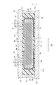
積層コンデンサC1は、図8に示されるように、基板31に埋め込まれて実装される。すなわち、積層コンデンサC1は、基板31に内蔵される。図8は、本実施形態に係る積層コンデンサの実装構造を説明するための図である。
As shown in FIG. 8, the multilayer capacitor C1 is embedded in the
基板31は、複数の絶縁層33が積層されることにより構成されている。絶縁層33は、セラミック又は樹脂などの絶縁性材料からなり、接着などにより互いに一体化されている。
The
積層コンデンサC1は、基板31に形成された収容部31aに配置されており、収容部31aに充填された樹脂34により、基板31に固定されている。これにより、積層コンデンサC1が、基板31内に埋め込まれる。図8に示された実装構造では、積層コンデンサC1は、素体2の主面2bが収容部31aの底部と対向するように、収容部31aに配置されている。
The multilayer capacitor C1 is disposed in a
積層コンデンサC1は、基板31の表面に配置された電極35,37と、ビア導体45,47を通して、電気的に接続されている。図8に示された実装構造では、第一端子電極5の電極部分5aが、ビア導体45を通して電極35と電気的に接続され、第二端子電極7の電極部分7aが、ビア導体47を通して電極37と電気的に接続されている。
The multilayer capacitor C <b> 1 is electrically connected through
ビア導体45,47は、基板31に形成されたビアホール内に導電性金属(たとえば、Cu又はAuなど)を無電解めっきなどにより成長させることにより、形成される。ビアホールは、レーザ加工により、基板31の表面側から積層コンデンサC1の第一及び第二端子電極5,7の電極部分5a,7aに達するように形成される。
The via
積層コンデンサC1では、電極部分5a,7aは、めっき層としての第三電極層25と、を有している。したがって、ビアホールに形成されるビア導体45,47と電極部分5a,7aとを確実に接続することができる。特に、ビア導体45,47がめっきにより形成される場合、ビア導体45,47と電極部分5a,7aとが、より一層確実に接続される。
In the multilayer capacitor C1, the
ここで、電極部分5a,5b,7a,7bの表面粗さ及び電極部分5c,5d,7c,7dの表面粗さについて詳細に説明する。
Here, the surface roughness of the
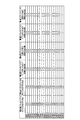
本発明者らは、電極部分5a,5b,7a,7bの表面粗さの範囲と、電極部分5c,5d,7c,7dの表面粗さの範囲とを明らかにするために、以下のような試験をおこなった。すなわち、電極部分5a,5b,5c,5d,7a,7b,7c,7dの表面粗さが異なる試料1〜12を用意し、各試料1〜12における、空隙の発生数及び剥離の発生数を確認した。その結果を図9に示す。図9は、各試料における空隙の発生数及び剥離の発生数を示す図表である。
In order to clarify the surface roughness range of the
電極部分5a,5b,5c,5d,7a,7b,7c,7dの表面粗さは、たとえば、第一電極層21を形成する際に用いられる導電性ペーストを異ならせることにより、変えることが可能である。表面粗さは導電ペーストに含まれている金属粉末(たとえば、Ni粉末又はCu粉など)の粒径の大きさによって変わる。すなわち、金属粉末の粒径が大きいほど、表面粗さは大きくなる。したがって、たとえば、電極部分5a,5b,7a,7bを形成する際に用いられる導電性ペーストと、電極部分5c,5d,7c,7dを形成する際に用いられる導電性ペーストとで、金属粉末の粒径を変えることにより、表面粗さを変えることが可能である。第一電極層21を形成する際に用いられる導電性ペーストを異ならせる以外に、第一電極層21を形成した後に、第一電極層21の表面を粗化処理又は研磨処理を行うことによっても、表面粗さを変えることが可能である。
The surface roughness of the
電極部分5a,5b,5c,5d,7a,7b,7c,7dの表面粗さは、算術平均粗さ(Ra)を用いた。算術平均粗さ(Ra)は、JIS B 0601:2013(ISO 4287:1997)に定義されている。
As the surface roughness of the
各試料1〜19は、複数の検体を含むロットである。各試料1〜19の検体は、上述した表面粗さが異なる点を除いて同じ構成である。各試料1〜19の検体では、素体2の第一方向D1の長さが0.17mmに設定され、素体2の第二方向D2の長さが0.49mmに設定され、素体2の第三方向D3の長さが0.98mmに設定されている。
Each sample 1-19 is a lot containing a plurality of specimens. The specimens of the samples 1 to 19 have the same configuration except that the surface roughness described above is different. In the specimens of the samples 1 to 19, the length of the
試料1の各検体では、電極部分5a,5b,7a,7bの表面の算術平均粗さが0.15μmに設定され、電極部分5c,5d,7c,7dの表面の算術平均粗さが0.19μmに設定されている。試料2の各検体では、電極部分5a,5b,7a,7bの表面の算術平均粗さが0.15μmに設定され、電極部分5c,5d,7c,7dの表面の算術平均粗さが0.25μmに設定されている。試料3の各検体では、電極部分5a,5b,7a,7bの表面の算術平均粗さが0.15μmに設定され、電極部分5c,5d,7c,7dの表面の算術平均粗さが0.38μmに設定されている。
In each specimen of the sample 1, the arithmetic average roughness of the surfaces of the
試料4の各検体では、電極部分5a,5b,7a,7bの表面の算術平均粗さが0.20μmに設定され、電極部分5c,5d,7c,7dの表面の算術平均粗さが0.18μmに設定されている。試料5の各検体では、電極部分5a,5b,7a,7bの表面の算術平均粗さが0.20μmに設定され、電極部分5c,5d,7c,7dの表面の算術平均粗さが0.27μmに設定されている。試料6の各検体では、電極部分5a,5b,7a,7bの表面の算術平均粗さが0.20μmに設定され、電極部分5c,5d,7c,7dの表面の算術平均粗さが0.34μmに設定されている。
In each specimen of the sample 4, the arithmetic average roughness of the surfaces of the
試料7の各検体では、電極部分5a,5b,7a,7bの表面の算術平均粗さが0.20μmに設定され、電極部分5c,5d,7c,7dの表面の算術平均粗さが0.38μmに設定されている。試料8の各検体では、電極部分5a,5b,7a,7bの表面の算術平均粗さが0.20μmに設定され、電極部分5c,5d,7c,7dの表面の算術平均粗さが0.40μmに設定されている。試料9の各検体では、電極部分5a,5b,7a,7bの表面の算術平均粗さが0.23μmに設定され、電極部分5c,5d,7c,7dの表面の算術平均粗さが0.25μmに設定されている。
In each specimen of the
試料10の各検体では、電極部分5a,5b,7a,7bの表面の算術平均粗さが0.23μmに設定され、電極部分5c,5d,7c,7dの表面の算術平均粗さが0.28μmに設定されている。試料11の各検体では、電極部分5a,5b,7a,7bの表面の算術平均粗さが0.23μmに設定され、電極部分5c,5d,7c,7dの表面の算術平均粗さが0.32μmに設定されている。試料12の各検体では、電極部分5a,5b,7a,7bの表面の算術平均粗さが0.23μmに設定され、電極部分5c,5d,7c,7dの表面の算術平均粗さが0.37μmに設定されている。
In each specimen of the sample 10, the arithmetic average roughness of the surfaces of the
試料13の各検体では、電極部分5a,5b,7a,7bの表面の算術平均粗さが0.23μmに設定され、電極部分5c,5d,7c,7dの表面の算術平均粗さが0.40μmに設定されている。試料14の各検体では、電極部分5a,5b,7a,7bの表面の算術平均粗さが0.26μmに設定され、電極部分5c,5d,7c,7dの表面の算術平均粗さが0.25μmに設定されている。試料15の各検体では、電極部分5a,5b,7a,7bの表面の算術平均粗さが0.26μmに設定され、電極部分5c,5d,7c,7dの表面の算術平均粗さが0.27μmに設定されている。
In each specimen of the
試料16の各検体では、電極部分5a,5b,7a,7bの表面の算術平均粗さが0.26μmに設定され、電極部分5c,5d,7c,7dの表面の算術平均粗さが0.32μmに設定されている。試料17の各検体では、電極部分5a,5b,7a,7bの表面の算術平均粗さが0.26μmに設定され、電極部分5c,5d,7c,7dの表面の算術平均粗さが0.28μmに設定されている。試料18の各検体では、電極部分5a,5b,7a,7bの表面の算術平均粗さが0.26μmに設定され、電極部分5c,5d,7c,7dの表面の算術平均粗さが0.40μmに設定されている。試料19の各検体では、電極部分5a,5b,7a,7bの表面の算術平均粗さが0.30μmに設定され、電極部分5c,5d,7c,7dの表面の算術平均粗さが0.27μmに設定されている。
In each specimen of the sample 16, the arithmetic average roughness of the surfaces of the
空隙の発生数は、次のようにして求めた。まず、試料1〜19ごとに、10個の検体を選び、選んだ検体を基板31の収容部31aに配置した後に、収容部31aに樹脂34を充填して、検体を基板31に埋め込んだ。その後、第一及び第二端子電極5,7に達するビアホールをレーザ加工により基板31(樹脂34)に形成し、ビアホール内にビア導体45,47を無電解めっきにより形成し、第一及び第二端子電極5,7とビア導体45,47とを接続し、検体が実装された基板31を得た。樹脂34として、エポキシ樹脂を用いた。
The number of voids was determined as follows. First, ten specimens were selected for each of the samples 1 to 19, and the selected specimens were placed in the
検体が実装された基板31を、検体(第一及び第二端子電極5,7)とビア導体45,47とを含む位置で切断し、切断面での空隙の有無を目視にて確認した。空隙の発生が確認された検体の数をカウントした。ここでは、第一及び第二端子電極5,7(電極部分5a,5b,7a,7b)とビア導体45,47との間に空隙が発生しているか否か、及び、第一及び第二端子電極5,7(電極部分5c,5d,7c,7d)と樹脂34との間に空隙が発生しているか否かを確認した。
The
電極部分5a,5b,7a,7bの表面の算術平均粗さが0.30μm以上である場合、電極部分5a,5b,7a,7bとビア導体45,47との間に空隙が発生している検体が存在することがわかった。電極部分5a,5b,7a,7bの表面の算術平均粗さが0.30μm以上である場合、電極部分5a,5b,7a,7bの表面の凹凸により、ビア導体45,47を形成する際に、金属が電極部分5a,5b,7a,7bに適切に析出され難いために、空隙が発生すると推測される。試料1〜18では、電極部分5a,5b,7a,7bとビア導体45,47との間に空隙が発生している検体は確認できなかった。
When the arithmetic average roughness of the surface of the
電極部分5c,5d,7c,7dの表面の算術平均粗さが0.40μm以上である場合、電極部分5c,5d,7c,7dと樹脂34との間に空隙が発生している検体が存在することがわかった。電極部分5c,5d,7c,7dの表面の算術平均粗さが0.40μm以上である場合、電極部分5c,5d,7c,7dの表面の凹凸の凹部に樹脂34が十分に入り込まないために、空隙が発生すると推測される。試料1〜7、試料9〜12、試料14〜17、及び試料19では、電極部分5c,5d,7c,7dと樹脂34との間に空隙が発生している検体は確認できなかった。
When the arithmetic average roughness of the surface of the
剥離の発生数は、次のようにして求めた。まず、空隙の発生が確認できなかった試料1〜7、試料9〜12、及び試料14〜17ごとに、10個の検体を選び、上述した手順と同じ手順により、検体が実装された基板31を得た。検体が実装された基板31に対し、窒素雰囲気下においてリフロー試験を5回実施した。リフロー試験の条件は、以下の通りである。まず、前処理として、予熱を125℃、24時間で行い、その後、ピーク温度260℃のリフローを行った。
The number of occurrences of peeling was determined as follows. First, 10 samples are selected for each of Samples 1 to 7, Samples 9 to 12, and Samples 14 to 17 for which no voids have been confirmed, and the
リフロー試験後に、検体が実装された基板31を、検体(第一及び第二端子電極5,7)とビア導体45,47とを含む位置で切断し、切断面での剥離の有無を目視にて確認した。剥離の発生が確認された検体の数をカウントした。ここでは、第一及び第二端子電極5,7(電極部分5a,5b,7a,7b)とビア導体45,47との間に剥離が発生しているか否か、及び、第一及び第二端子電極5,7(電極部分5c,5d,7c,7d)と樹脂34との間に剥離が発生しているか否かを確認した。
After the reflow test, the
電極部分5a,5b,7a,7bの表面の算術平均粗さが0.15μm以下である場合、電極部分5a,5b,7a,7bとビア導体45,47との間に剥離が発生している検体が存在することがわかった。電極部分5a,5b,7a,7bの表面の算術平均粗さが0.15μm以下である場合、電極部分5a,5b,7a,7bとビア導体45,47との密着性が十分に得られないため、電極部分5a,5b,7a,7bとビア導体45,47との界面から剥離が発生すると推測される。試料4〜7、試料9〜12、及び試料14〜17では、電極部分5a,5b,7a,7bとビア導体45,47との間に剥離が発生している検体は確認できなかった。
When the arithmetic average roughness of the surface of the
電極部分5c,5d,7c,7dの表面の算術平均粗さが0.25μm以下である場合、電極部分5c,5d,7c,7dと樹脂34との間に剥離が発生している検体が存在することがわかった。電極部分5c,5d,7c,7dの表面の算術平均粗さが0.25μm以下である場合、電極部分5c,5d,7c,7dの表面の凹凸の凹部に樹脂34が入り込むものの、入り込む樹脂34の量が少なく、電極部分5c,5d,7c,7dと樹脂34との密着性が十分に得られないため、電極部分5c,5d,7c,7dと樹脂34との界面から剥離が発生すると推測される。試料3、試料5〜7、試料10〜12、及び試料15〜17では、電極部分5c,5d,7c,7dと樹脂34との間に空隙が発生している検体は確認できなかった。
When the arithmetic average roughness of the surfaces of the
試料5〜7、試料10〜12、及び試料15〜17では、空隙及び剥離が発生している検体は確認できなかった。 In Samples 5-7, Samples 10-12, and Samples 15-17, the specimen in which voids and peeling occurred could not be confirmed.
以上のことから、電極部分5a,5b,7a,7bの表面の算術平均粗さが、0.20〜0.26μmであり、電極部分5c,5d,7c,7dの表面の算術平均粗さが、0.27〜0.38μmであることにより、電極部分5a,5b,7a,7bとビア導体45,47との間と、電極部分5c,5d,7c,7dと樹脂34との間とに、空隙が発生するのを防ぐことができると共に、電極部分5a,5b,7a,7bとビア導体45,47との剥離と、電極部分5c,5d,7c,7dと樹脂34との剥離とが生じるのを防ぐことができる。この結果、基板31に形成されるビア導体45との接続性を確保しつつ、積層コンデンサC1の基板31への内蔵を適切に行うことができる。
From the above, the arithmetic average roughness of the surfaces of the
続いて、素体2の表面粗さ、特に、素体2における第一及び第二端子電極5,7から露出している部分の表面粗さについて詳細に説明する。
Next, the surface roughness of the
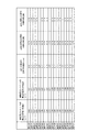
本発明者らは、素体2における第一及び第二端子電極5,7から露出している部分の表面粗さの範囲を明らかにするために、以下のような試験をおこなった。すなわち、素体2の表面粗さが異なる試料20〜37を用意し、各試料20〜37における、空隙の発生数及び剥離の発生数を確認した。その結果を図10に示す。図10は、各試料における空隙の発生数及び剥離の発生数を示す図表である。ここでも、表面粗さは、上述した算術平均粗さ(Ra)を用いた。素体2の表面粗さは、たとえば、素体を形成する際に、セラミックグリーンシートに異なる誘電体材料を用いる、又は、セラミックグリーンシートを積層した積層体を研磨することにより、変えることが可能である。
In order to clarify the surface roughness range of the portions exposed from the first and second
各試料20〜37は、複数の検体を含むロットである。各試料20〜24の検体は、素体2の表面粗さが異なる点を除いて同じ構成である。各試料25〜28の検体は、素体2の表面粗さが異なる点を除いて同じ構成である。各試料29〜33の検体は、素体2の表面粗さが異なる点を除いて同じ構成である。各試料34〜37の検体は、素体2の表面粗さが異なる点を除いて同じ構成である。各試料20〜37の検体では、素体2の第一方向D1の長さが0.17mmに設定され、素体2の第二方向D2の長さが0.49mmに設定され、素体2の第三方向D3の長さが0.98mmに設定されている。
Each sample 20 to 37 is a lot containing a plurality of specimens. The specimens of the samples 20 to 24 have the same configuration except that the surface roughness of the
試料20〜24の各検体では、電極部分5a,5b,7a,7bの表面の算術平均粗さが0.20μmに設定され、電極部分5c,5d,7c,7dの表面の算術平均粗さが0.27μmに設定されている。試料25〜28の各検体では、電極部分5a,5b,7a,7bの表面の算術平均粗さが0.26μmに設定され、電極部分5c,5d,7c,7dの表面の算術平均粗さが0.27μmに設定されている。試料29〜33の各検体では、電極部分5a,5b,7a,7bの表面の算術平均粗さが0.20μmに設定され、電極部分5c,5d,7c,7dの表面の算術平均粗さが0.38μmに設定されている。試料34〜37の各検体では、電極部分5a,5b,7a,7bの表面の算術平均粗さが0.26μmに設定され、電極部分5c,5d,7c,7dの表面の算術平均粗さが0.38μmに設定されている。
In each specimen of samples 20 to 24, the arithmetic average roughness of the surfaces of the
試料20の各検体では、素体2の表面の算術平均粗さが0.12μmに設定されている。試料21の各検体では、素体2の表面の算術平均粗さが0.14μmに設定されている。試料22の各検体では、素体2の表面の算術平均粗さが0.16μmに設定されている。試料23の各検体では、素体2の表面の算術平均粗さが0.19μmに設定されている。試料24の各検体では、素体2の表面の算術平均粗さが0.27μmに設定されている。試料25の各検体では、素体2の表面の算術平均粗さが0.14μmに設定されている。試料26の各検体では、素体2の表面の算術平均粗さが0.17μmに設定されている。試料27の各検体では、素体2の表面の算術平均粗さが0.19μmに設定されている。試料28の各検体では、素体2の表面の算術平均粗さが0.21μmに設定されている。
In each specimen of the sample 20, the arithmetic average roughness of the surface of the
試料29の各検体では、素体2の表面の算術平均粗さが0.11μmに設定されている。試料30の各検体では、素体2の表面の算術平均粗さが0.14μmに設定されている。試料31の各検体では、素体2の表面の算術平均粗さが0.15μmに設定されている。試料32の各検体では、素体2の表面の算術平均粗さが0.18μmに設定されている。試料33の各検体では、素体2の表面の算術平均粗さが0.25μmに設定されている。試料34の各検体では、素体2の表面の算術平均粗さが0.14μmに設定されている。試料35の各検体では、素体2の表面の算術平均粗さが0.17μmに設定されている。試料36の各検体では、素体2の表面の算術平均粗さが0.19μmに設定されている。試料37の各検体では、素体2の表面の算術平均粗さが0.22μmに設定されている。
In each specimen of the sample 29, the arithmetic average roughness of the surface of the
空隙の発生数は、次のようにして求めた。まず、試料20〜37ごとに、10個の検体を選び、上述した手順と同じ手順により、検体が実装された基板31を得た。検体が実装された基板31を、素体2における第一及び第二端子電極5,7から露出している部分を含む位置で切断し、切断面での空隙の有無を目視にて確認した。空隙の発生が確認された検体の数をカウントした。ここでは、素体2(第一及び第二端子電極5,7から露出している部分)と樹脂34との間に空隙が発生しているか否かを確認した。
The number of voids was determined as follows. First, ten specimens were selected for each of the samples 20 to 37, and the
素体2(第一及び第二端子電極5,7から露出している部分)の表面の算術平均粗さが0.21μm以上である場合、素体2と樹脂34との間に空隙が発生している検体が存在することがわかった。素体2の表面の算術平均粗さが0.21μm以上である場合、素体2の表面の凹凸の凹部に樹脂34が十分に入り込まないために、空隙が発生すると推測される。試料20〜23、試料25〜27、試料29〜32、及び試料34〜36では、素体2と樹脂34との間に空隙が発生している検体は確認できなかった。
When the arithmetic mean roughness of the surface of the element body 2 (the parts exposed from the first and second
剥離の発生数は、次のようにして求めた。まず、空隙の発生が確認できなかった試料20〜23、試料25〜27、試料29〜32、及び試料34〜36ごとに、10個の検体を選び、上述した手順と同じ手順により、検体が実装された基板31を得た。検体が実装された基板31に対し、窒素雰囲気下においてリフロー試験を5回実施した。リフロー試験の条件は、以下の通りである。まず、前処理として、予熱を125℃、24時間で行い、その後、ピーク温度260℃のリフローを行った。
The number of occurrences of peeling was determined as follows. First, 10 samples are selected for each of Samples 20 to 23,
リフロー試験後に、検体が実装された基板31を、素体2における第一及び第二端子電極5,7から露出している部分を含む位置で切断し、切断面での剥離の有無を目視にて確認した。剥離の発生が確認された検体の数をカウントした。ここでは、素体2(第一及び第二端子電極5,7から露出している部分)と樹脂34との間に剥離が発生しているか否かを確認した。
After the reflow test, the
素体2の表面の算術平均粗さが0.12μm以下である場合、素体2と樹脂34との間に剥離が発生している検体が存在することがわかった。素体2の表面の算術平均粗さが0.12μm以下である場合、素体2の表面の凹凸の凹部に樹脂34が入り込むものの、入り込む樹脂34の量が少なく、素体2と樹脂34との密着性が十分に得られないため、素体2と樹脂34との界面から剥離が発生すると推測される。試料21〜23、試料25〜27、試料30〜32、及び試料34〜36では、素体2と樹脂34との間に空隙が発生している検体は確認できなかった。
It was found that when the arithmetic average roughness of the surface of the
試料21〜23、試料25〜27、試料30〜32、及び試料34〜36では、空隙及び剥離が発生している検体は確認できなかった。
In
以上のことから、素体2(第一及び第二端子電極5,7から露出している部分)の表面の算術平均粗さが、0.14〜0.19μmであることにより、素体2と樹脂34との間に空隙が発生するのを防ぐことができると共に、素体2と樹脂34との剥離が生じるのを防ぐことができる。この結果、積層コンデンサC1の基板への内蔵をより一層適切に行うことができる。
From the above, when the arithmetic mean roughness of the surface of the element body 2 (the portions exposed from the first and second
以上、本発明の実施形態について説明してきたが、本発明は必ずしも上述した実施形態に限定されるものではなく、その要旨を逸脱しない範囲で様々な変更が可能である。 As mentioned above, although embodiment of this invention has been described, this invention is not necessarily limited to embodiment mentioned above, A various change is possible in the range which does not deviate from the summary.
第一及び第二端子電極5,7は、電極部分5d,7dを有している必要はない。すなわち、第一端子電極5は、三つの面2a,2b,2cに形成されていてもよく、第二端子電極7は、三つの面2a,2b,2dに形成されていてもよい。
The 1st and 2nd
2…素体、2a,2b…主面、2c,2d…第一側面、2e,2f…第二側面、5…第一端子電極、5a,5b,5c,5d…電極部分、7…第二端子電極、7a,7b,7c,7d…電極部分、11…第一内部電極、13…第二内部電極、31…基板、31a…収容部、34…樹脂、45,47…ビア導体、C1…積層コンデンサ。 2 ... Element body, 2a, 2b ... Main surface, 2c, 2d ... First side surface, 2e, 2f ... Second side surface, 5 ... First terminal electrode, 5a, 5b, 5c, 5d ... Electrode portion, 7 ... Second Terminal electrode, 7a, 7b, 7c, 7d ... electrode portion, 11 ... first internal electrode, 13 ... second internal electrode, 31 ... substrate, 31a ... housing part, 34 ... resin, 45, 47 ... via conductor, C1 ... Multilayer capacitor.
Claims (2)
前記一対の主面が対向している前記方向で互いに対向するように前記素体内に交互に配置されている複数の内部電極と、
前記素体の互いに対向する一対の前記側面側にそれぞれ配置されていると共に前記複数の内部電極のうち対応する内部電極に接続されている一対の端子電極と、を備え、
前記一対の主面が対向している前記方向での前記素体の長さは、前記一対の側面が対向している方向での前記素体の長さ及び前記一対の側面とは別の一対の側面が対向している方向での前記素体の長さよりも小さく、
各前記端子電極は、前記主面に配置されている第一電極部分と、前記側面に配置されている第二電極部分とを有し、
前記第一電極部分の表面の算術平均粗さが、0.20〜0.26μmであり、
前記第二電極部分の表面の算術平均粗さが、0.27〜0.38μmである、積層コンデンサ。 It has a rectangular parallelepiped shape, and has a pair of main surfaces facing each other and four side surfaces extending in a direction in which the pair of main surfaces oppose each other so as to connect the pair of main surfaces. And the body
A plurality of internal electrodes alternately arranged in the element body so as to face each other in the direction in which the pair of main surfaces are opposed to each other;
A pair of terminal electrodes disposed on a pair of side surfaces facing each other of the element body and connected to a corresponding internal electrode among the plurality of internal electrodes,
The length of the element body in the direction in which the pair of main surfaces face each other is different from the length of the element body in the direction in which the pair of side surfaces face each other and the pair of side surfaces. Smaller than the length of the element body in the direction in which the side surfaces of
Each of the terminal electrodes has a first electrode portion disposed on the main surface and a second electrode portion disposed on the side surface,
The arithmetic average roughness of the surface of the first electrode portion is 0.20 to 0.26 μm,
The multilayer capacitor whose arithmetic mean roughness of the surface of said 2nd electrode part is 0.27-0.38 micrometer.
Priority Applications (3)
| Application Number | Priority Date | Filing Date | Title |
|---|---|---|---|
| JP2015062562A JP2016181663A (en) | 2015-03-25 | 2015-03-25 | Multilayer capacitor |
| US15/040,358 US9928961B2 (en) | 2015-03-25 | 2016-02-10 | Multilayer capacitor |
| CN201610173152.0A CN106024384B (en) | 2015-03-25 | 2016-03-24 | Cascade capacitor |
Applications Claiming Priority (1)
| Application Number | Priority Date | Filing Date | Title |
|---|---|---|---|
| JP2015062562A JP2016181663A (en) | 2015-03-25 | 2015-03-25 | Multilayer capacitor |
Publications (1)
| Publication Number | Publication Date |
|---|---|
| JP2016181663A true JP2016181663A (en) | 2016-10-13 |
Family
ID=56974321
Family Applications (1)
| Application Number | Title | Priority Date | Filing Date |
|---|---|---|---|
| JP2015062562A Pending JP2016181663A (en) | 2015-03-25 | 2015-03-25 | Multilayer capacitor |
Country Status (3)
| Country | Link |
|---|---|
| US (1) | US9928961B2 (en) |
| JP (1) | JP2016181663A (en) |
| CN (1) | CN106024384B (en) |
Cited By (1)
| Publication number | Priority date | Publication date | Assignee | Title |
|---|---|---|---|---|
| US11335510B2 (en) | 2019-08-02 | 2022-05-17 | Samsung Electro-Mechanics Co., Ltd. | Multilayer ceramic capacitor |
Families Citing this family (4)
| Publication number | Priority date | Publication date | Assignee | Title |
|---|---|---|---|---|
| CN112185704B (en) * | 2019-07-04 | 2023-02-17 | 三星电机株式会社 | Multilayer ceramic capacitor |
| KR102333086B1 (en) * | 2019-08-19 | 2021-12-01 | 삼성전기주식회사 | Multi-layered ceramic capacitor |
| JP7379899B2 (en) * | 2019-07-22 | 2023-11-15 | Tdk株式会社 | ceramic electronic components |
| KR102772045B1 (en) * | 2019-09-19 | 2025-02-25 | 삼성전기주식회사 | Multi-layer ceramic electronic component |
Citations (4)
| Publication number | Priority date | Publication date | Assignee | Title |
|---|---|---|---|---|
| JP2001332437A (en) * | 2000-05-19 | 2001-11-30 | Ibiden Co Ltd | Capacitors and multilayer printed wiring boards |
| JP2014075446A (en) * | 2012-10-03 | 2014-04-24 | Sumitomo Electric Printed Circuit Inc | Printed wiring board and method for manufacturing the same |
| JP2014239139A (en) * | 2013-06-07 | 2014-12-18 | 株式会社村田製作所 | Capacitor and method of manufacturing the same |
| JP2014239258A (en) * | 2012-12-27 | 2014-12-18 | サムソン エレクトロ−メカニックス カンパニーリミテッド. | Manufacturing method of electronic component built-in printed circuit board |
Family Cites Families (9)
| Publication number | Priority date | Publication date | Assignee | Title |
|---|---|---|---|---|
| JP2001126946A (en) * | 1999-10-28 | 2001-05-11 | Murata Mfg Co Ltd | Laminated ceramic electronic component and method for manufacturing the same |
| JP2001217135A (en) * | 2000-02-03 | 2001-08-10 | Murata Mfg Co Ltd | Laminated ceramic electronic component and manufacturing method therefor |
| JP4649847B2 (en) | 2004-02-25 | 2011-03-16 | 株式会社村田製作所 | Chip-type electronic components |
| JP5471586B2 (en) * | 2010-02-25 | 2014-04-16 | Tdk株式会社 | Chip-type electronic components |
| KR101548804B1 (en) * | 2013-09-16 | 2015-08-31 | 삼성전기주식회사 | Embedded multilayer ceramic electronic part and print circuit board having embedded multilayer ceramic electronic part |
| KR20150041490A (en) * | 2013-10-08 | 2015-04-16 | 삼성전기주식회사 | Embedded multilayer ceramic electronic part and print circuit board having embedded multilayer ceramic electronic part |
| US9881739B2 (en) * | 2014-09-30 | 2018-01-30 | Murata Manufacturing Co., Ltd. | Multilayer ceramic capacitor |
| US9859056B2 (en) * | 2014-09-30 | 2018-01-02 | Murata Manufacturing Co., Ltd. | Multilayer ceramic capacitor |
| US9627136B2 (en) * | 2014-09-30 | 2017-04-18 | Murata Manufacturing Co., Ltd. | Multilayer ceramic capacitor |
-
2015
- 2015-03-25 JP JP2015062562A patent/JP2016181663A/en active Pending
-
2016
- 2016-02-10 US US15/040,358 patent/US9928961B2/en active Active
- 2016-03-24 CN CN201610173152.0A patent/CN106024384B/en active Active
Patent Citations (4)
| Publication number | Priority date | Publication date | Assignee | Title |
|---|---|---|---|---|
| JP2001332437A (en) * | 2000-05-19 | 2001-11-30 | Ibiden Co Ltd | Capacitors and multilayer printed wiring boards |
| JP2014075446A (en) * | 2012-10-03 | 2014-04-24 | Sumitomo Electric Printed Circuit Inc | Printed wiring board and method for manufacturing the same |
| JP2014239258A (en) * | 2012-12-27 | 2014-12-18 | サムソン エレクトロ−メカニックス カンパニーリミテッド. | Manufacturing method of electronic component built-in printed circuit board |
| JP2014239139A (en) * | 2013-06-07 | 2014-12-18 | 株式会社村田製作所 | Capacitor and method of manufacturing the same |
Cited By (2)
| Publication number | Priority date | Publication date | Assignee | Title |
|---|---|---|---|---|
| US11335510B2 (en) | 2019-08-02 | 2022-05-17 | Samsung Electro-Mechanics Co., Ltd. | Multilayer ceramic capacitor |
| US11763995B2 (en) | 2019-08-02 | 2023-09-19 | Samsung Electro-Mechanics Co., Ltd. | Multilayer ceramic capacitor |
Also Published As
| Publication number | Publication date |
|---|---|
| US20160284475A1 (en) | 2016-09-29 |
| CN106024384A (en) | 2016-10-12 |
| CN106024384B (en) | 2018-06-08 |
| US9928961B2 (en) | 2018-03-27 |
Similar Documents
| Publication | Publication Date | Title |
|---|---|---|
| JP5206440B2 (en) | Ceramic electronic components | |
| JP5931044B2 (en) | Multilayer ceramic electronic component for built-in substrate and printed circuit board with built-in multilayer ceramic electronic component | |
| US9892855B2 (en) | Electronic component | |
| US9431174B2 (en) | Multilayer capacitor | |
| KR101927731B1 (en) | Multilayer ceramic capacitor | |
| US9748042B2 (en) | Multilayer feedthrough capacitor | |
| US9972437B2 (en) | Multilayer capacitor with terminal electrode including sintered conductor layer | |
| JP2017073434A (en) | Electronic component | |
| US12249464B2 (en) | Electronic component | |
| US10026554B2 (en) | Multilayer capacitor with (1) an element body having internal electrodes and (2) opposing terminal electrodes | |
| US10984939B2 (en) | Multilayer coil component | |
| JP2022067931A (en) | Electronic component | |
| JP2016181663A (en) | Multilayer capacitor | |
| KR20190121175A (en) | Multi-layered ceramic capacitor | |
| JP6497127B2 (en) | Multilayer capacitor | |
| US10008329B2 (en) | Multilayer capacitor having first internal electrodes and second internal electrodes alternately disposed | |
| JP6142650B2 (en) | Multilayer feedthrough capacitor | |
| JP6136507B2 (en) | Multilayer capacitor array | |
| JP6115276B2 (en) | Multilayer capacitor | |
| JP2023056513A (en) | Laminated electronic component | |
| JP2016149425A (en) | Multilayer feedthrough capacitor | |
| JP2016136562A (en) | Multilayer capacitor | |
| JP6476954B2 (en) | Multilayer feedthrough capacitor | |
| CN116266502A (en) | Ceramic Electronic Components | |
| CN118575243A (en) | Ceramic electronic component |
Legal Events
| Date | Code | Title | Description |
|---|---|---|---|
| A621 | Written request for application examination |
Free format text: JAPANESE INTERMEDIATE CODE: A621 Effective date: 20171024 |
|
| A131 | Notification of reasons for refusal |
Free format text: JAPANESE INTERMEDIATE CODE: A131 Effective date: 20180731 |
|
| A02 | Decision of refusal |
Free format text: JAPANESE INTERMEDIATE CODE: A02 Effective date: 20181113 |