JP2016131266A - Oscillation device, oscillator, electronic apparatus and mobile body - Google Patents
Oscillation device, oscillator, electronic apparatus and mobile body Download PDFInfo
- Publication number
- JP2016131266A JP2016131266A JP2015003924A JP2015003924A JP2016131266A JP 2016131266 A JP2016131266 A JP 2016131266A JP 2015003924 A JP2015003924 A JP 2015003924A JP 2015003924 A JP2015003924 A JP 2015003924A JP 2016131266 A JP2016131266 A JP 2016131266A
- Authority
- JP
- Japan
- Prior art keywords
- vibration element
- heater
- vibration
- oscillator
- axis
- Prior art date
- Legal status (The legal status is an assumption and is not a legal conclusion. Google has not performed a legal analysis and makes no representation as to the accuracy of the status listed.)
- Withdrawn
Links
- 230000010355 oscillation Effects 0.000 title abstract description 25
- 239000000758 substrate Substances 0.000 claims abstract description 26
- 230000008646 thermal stress Effects 0.000 abstract description 16
- 230000020169 heat generation Effects 0.000 abstract description 3
- 239000013078 crystal Substances 0.000 description 53
- 239000000853 adhesive Substances 0.000 description 19
- 230000001070 adhesive effect Effects 0.000 description 19
- 238000010438 heat treatment Methods 0.000 description 18
- 239000010453 quartz Substances 0.000 description 16
- VYPSYNLAJGMNEJ-UHFFFAOYSA-N silicon dioxide Inorganic materials O=[Si]=O VYPSYNLAJGMNEJ-UHFFFAOYSA-N 0.000 description 16
- 230000005284 excitation Effects 0.000 description 13
- 239000000463 material Substances 0.000 description 13
- 238000000034 method Methods 0.000 description 12
- 230000008569 process Effects 0.000 description 10
- 230000008859 change Effects 0.000 description 9
- 230000006870 function Effects 0.000 description 8
- 238000004519 manufacturing process Methods 0.000 description 8
- 229910052751 metal Inorganic materials 0.000 description 8
- 239000002184 metal Substances 0.000 description 8
- 239000000919 ceramic Substances 0.000 description 7
- 238000000605 extraction Methods 0.000 description 7
- 229910000833 kovar Inorganic materials 0.000 description 7
- 238000001035 drying Methods 0.000 description 5
- 238000003384 imaging method Methods 0.000 description 5
- 229910052709 silver Inorganic materials 0.000 description 5
- PXHVJJICTQNCMI-UHFFFAOYSA-N Nickel Chemical compound [Ni] PXHVJJICTQNCMI-UHFFFAOYSA-N 0.000 description 4
- KDLHZDBZIXYQEI-UHFFFAOYSA-N Palladium Chemical compound [Pd] KDLHZDBZIXYQEI-UHFFFAOYSA-N 0.000 description 4
- 238000012986 modification Methods 0.000 description 4
- 230000004048 modification Effects 0.000 description 4
- 230000003287 optical effect Effects 0.000 description 4
- 238000012545 processing Methods 0.000 description 4
- 239000004332 silver Substances 0.000 description 4
- 229910000679 solder Inorganic materials 0.000 description 4
- BQCADISMDOOEFD-UHFFFAOYSA-N Silver Chemical compound [Ag] BQCADISMDOOEFD-UHFFFAOYSA-N 0.000 description 3
- 238000004891 communication Methods 0.000 description 3
- 239000011521 glass Substances 0.000 description 3
- 239000010931 gold Substances 0.000 description 3
- 238000003466 welding Methods 0.000 description 3
- 230000032683 aging Effects 0.000 description 2
- 239000000956 alloy Substances 0.000 description 2
- 239000012298 atmosphere Substances 0.000 description 2
- 230000008901 benefit Effects 0.000 description 2
- 230000001413 cellular effect Effects 0.000 description 2
- 239000004020 conductor Substances 0.000 description 2
- 229910052737 gold Inorganic materials 0.000 description 2
- 239000007769 metal material Substances 0.000 description 2
- 238000012544 monitoring process Methods 0.000 description 2
- 229910052759 nickel Inorganic materials 0.000 description 2
- 229910052763 palladium Inorganic materials 0.000 description 2
- BASFCYQUMIYNBI-UHFFFAOYSA-N platinum Chemical compound [Pt] BASFCYQUMIYNBI-UHFFFAOYSA-N 0.000 description 2
- 230000009467 reduction Effects 0.000 description 2
- 229920005989 resin Polymers 0.000 description 2
- 239000011347 resin Substances 0.000 description 2
- 238000007789 sealing Methods 0.000 description 2
- 230000035882 stress Effects 0.000 description 2
- WSMQKESQZFQMFW-UHFFFAOYSA-N 5-methyl-pyrazole-3-carboxylic acid Chemical compound CC1=CC(C(O)=O)=NN1 WSMQKESQZFQMFW-UHFFFAOYSA-N 0.000 description 1
- 229910000851 Alloy steel Inorganic materials 0.000 description 1
- IJGRMHOSHXDMSA-UHFFFAOYSA-N Atomic nitrogen Chemical compound N#N IJGRMHOSHXDMSA-UHFFFAOYSA-N 0.000 description 1
- OKTJSMMVPCPJKN-UHFFFAOYSA-N Carbon Chemical compound [C] OKTJSMMVPCPJKN-UHFFFAOYSA-N 0.000 description 1
- 229910017824 Cu—Fe—P Inorganic materials 0.000 description 1
- 239000004593 Epoxy Substances 0.000 description 1
- WQZGKKKJIJFFOK-GASJEMHNSA-N Glucose Natural products OC[C@H]1OC(O)[C@H](O)[C@@H](O)[C@@H]1O WQZGKKKJIJFFOK-GASJEMHNSA-N 0.000 description 1
- 239000004642 Polyimide Substances 0.000 description 1
- 229910045601 alloy Inorganic materials 0.000 description 1
- 230000006399 behavior Effects 0.000 description 1
- 239000011230 binding agent Substances 0.000 description 1
- 230000005540 biological transmission Effects 0.000 description 1
- 239000008280 blood Substances 0.000 description 1
- 210000004369 blood Anatomy 0.000 description 1
- 230000036772 blood pressure Effects 0.000 description 1
- 238000005219 brazing Methods 0.000 description 1
- 239000003990 capacitor Substances 0.000 description 1
- 229910052799 carbon Inorganic materials 0.000 description 1
- 239000003795 chemical substances by application Substances 0.000 description 1
- 230000007797 corrosion Effects 0.000 description 1
- 238000005260 corrosion Methods 0.000 description 1
- 229910001873 dinitrogen Inorganic materials 0.000 description 1
- 230000000694 effects Effects 0.000 description 1
- 239000010419 fine particle Substances 0.000 description 1
- 239000008103 glucose Substances 0.000 description 1
- PCHJSUWPFVWCPO-UHFFFAOYSA-N gold Chemical compound [Au] PCHJSUWPFVWCPO-UHFFFAOYSA-N 0.000 description 1
- 239000011261 inert gas Substances 0.000 description 1
- 229910010272 inorganic material Inorganic materials 0.000 description 1
- 239000011147 inorganic material Substances 0.000 description 1
- 238000005304 joining Methods 0.000 description 1
- 238000010030 laminating Methods 0.000 description 1
- GQYHUHYESMUTHG-UHFFFAOYSA-N lithium niobate Chemical compound [Li+].[O-][Nb](=O)=O GQYHUHYESMUTHG-UHFFFAOYSA-N 0.000 description 1
- 238000005259 measurement Methods 0.000 description 1
- 238000010295 mobile communication Methods 0.000 description 1
- 239000002245 particle Substances 0.000 description 1
- 230000002093 peripheral effect Effects 0.000 description 1
- 229910052697 platinum Inorganic materials 0.000 description 1
- 229920001721 polyimide Polymers 0.000 description 1
- 229920001296 polysiloxane Polymers 0.000 description 1
- 239000000843 powder Substances 0.000 description 1
- 230000002265 prevention Effects 0.000 description 1
- 239000010944 silver (metal) Substances 0.000 description 1
- -1 silver halide Chemical class 0.000 description 1
- 238000005245 sintering Methods 0.000 description 1
- 229910001220 stainless steel Inorganic materials 0.000 description 1
- 239000010935 stainless steel Substances 0.000 description 1
- 238000003860 storage Methods 0.000 description 1
- 229920003002 synthetic resin Polymers 0.000 description 1
- 239000000057 synthetic resin Substances 0.000 description 1
- 229910052718 tin Inorganic materials 0.000 description 1
- 239000011135 tin Substances 0.000 description 1
- 238000012546 transfer Methods 0.000 description 1
- WFKWXMTUELFFGS-UHFFFAOYSA-N tungsten Chemical compound [W] WFKWXMTUELFFGS-UHFFFAOYSA-N 0.000 description 1
- 229910052721 tungsten Inorganic materials 0.000 description 1
- 239000010937 tungsten Substances 0.000 description 1
Images


Classifications
-
- H—ELECTRICITY
- H03—ELECTRONIC CIRCUITRY
- H03H—IMPEDANCE NETWORKS, e.g. RESONANT CIRCUITS; RESONATORS
- H03H9/00—Networks comprising electromechanical or electro-acoustic devices; Electromechanical resonators
- H03H9/02—Details
- H03H9/02244—Details of microelectro-mechanical resonators
- H03H9/02433—Means for compensation or elimination of undesired effects
- H03H9/02448—Means for compensation or elimination of undesired effects of temperature influence
-
- H—ELECTRICITY
- H03—ELECTRONIC CIRCUITRY
- H03B—GENERATION OF OSCILLATIONS, DIRECTLY OR BY FREQUENCY-CHANGING, BY CIRCUITS EMPLOYING ACTIVE ELEMENTS WHICH OPERATE IN A NON-SWITCHING MANNER; GENERATION OF NOISE BY SUCH CIRCUITS
- H03B5/00—Generation of oscillations using amplifier with regenerative feedback from output to input
- H03B5/02—Details
- H03B5/04—Modifications of generator to compensate for variations in physical values, e.g. power supply, load, temperature
-
- H—ELECTRICITY
- H03—ELECTRONIC CIRCUITRY
- H03B—GENERATION OF OSCILLATIONS, DIRECTLY OR BY FREQUENCY-CHANGING, BY CIRCUITS EMPLOYING ACTIVE ELEMENTS WHICH OPERATE IN A NON-SWITCHING MANNER; GENERATION OF NOISE BY SUCH CIRCUITS
- H03B5/00—Generation of oscillations using amplifier with regenerative feedback from output to input
- H03B5/30—Generation of oscillations using amplifier with regenerative feedback from output to input with frequency-determining element being electromechanical resonator
- H03B5/32—Generation of oscillations using amplifier with regenerative feedback from output to input with frequency-determining element being electromechanical resonator being a piezoelectric resonator
-
- H—ELECTRICITY
- H03—ELECTRONIC CIRCUITRY
- H03H—IMPEDANCE NETWORKS, e.g. RESONANT CIRCUITS; RESONATORS
- H03H9/00—Networks comprising electromechanical or electro-acoustic devices; Electromechanical resonators
- H03H9/02—Details
- H03H9/02007—Details of bulk acoustic wave devices
- H03H9/02086—Means for compensation or elimination of undesirable effects
- H03H9/02102—Means for compensation or elimination of undesirable effects of temperature influence
-
- H—ELECTRICITY
- H03—ELECTRONIC CIRCUITRY
- H03H—IMPEDANCE NETWORKS, e.g. RESONANT CIRCUITS; RESONATORS
- H03H9/00—Networks comprising electromechanical or electro-acoustic devices; Electromechanical resonators
- H03H9/02—Details
- H03H9/05—Holders; Supports
- H03H9/0538—Constructional combinations of supports or holders with electromechanical or other electronic elements
- H03H9/0547—Constructional combinations of supports or holders with electromechanical or other electronic elements consisting of a vertical arrangement
- H03H9/0552—Constructional combinations of supports or holders with electromechanical or other electronic elements consisting of a vertical arrangement the device and the other elements being mounted on opposite sides of a common substrate
-
- H—ELECTRICITY
- H03—ELECTRONIC CIRCUITRY
- H03H—IMPEDANCE NETWORKS, e.g. RESONANT CIRCUITS; RESONATORS
- H03H9/00—Networks comprising electromechanical or electro-acoustic devices; Electromechanical resonators
- H03H9/02—Details
- H03H9/05—Holders; Supports
- H03H9/10—Mounting in enclosures
- H03H9/1007—Mounting in enclosures for bulk acoustic wave [BAW] devices
- H03H9/1014—Mounting in enclosures for bulk acoustic wave [BAW] devices the enclosure being defined by a frame built on a substrate and a cap, the frame having no mechanical contact with the BAW device
- H03H9/1021—Mounting in enclosures for bulk acoustic wave [BAW] devices the enclosure being defined by a frame built on a substrate and a cap, the frame having no mechanical contact with the BAW device the BAW device being of the cantilever type
Abstract
Description
本発明は、振動デバイス、発振器、電子機器、および移動体に関する。 The present invention relates to a vibrating device, an oscillator, an electronic apparatus, and a moving object.
水晶発振器は、安定な周波数を供給する周波数発生源として、放送機器、計測機器、デジタル機器のクロック信号源などに広く利用されている。特に、ヒーター付き水晶発振器(Oven Controlled Xtal Oscillator:以下、OCXOと言う)は、容器に小型のヒーターと水晶振動子とを収納して、振動素子の周囲温度を一定に保つことにより極めて良好な周波数安定性を持たせたものである。 A crystal oscillator is widely used as a frequency generation source for supplying a stable frequency, such as a clock signal source for broadcasting equipment, measurement equipment, and digital equipment. In particular, a crystal oscillator with a heater (Oven Controlled Xtal Oscillator: hereinafter referred to as OCXO) has a very good frequency by storing a small heater and a crystal resonator in a container and keeping the ambient temperature of the vibration element constant. It has been given stability.
このようなOCXOとして、例えば、特許文献1では、両端で支持された振動素子(圧電素子)の真下にヒーター(ヒーター素子)が備えられていることによって、容器(パッケージ)外への熱伝導が抑制され、かつ、エネルギーを抑えて振動素子(圧電素子)を加熱することができる振動デバイス(圧電デバイス)が提案されている。 As such OCXO, for example, in Patent Document 1, a heater (heater element) is provided directly below a vibration element (piezoelectric element) supported at both ends, so that heat conduction to the outside of the container (package) can be prevented. There has been proposed a vibration device (piezoelectric device) that is suppressed and can heat the vibration element (piezoelectric element) while suppressing energy.
しかしながら、特許文献1に記載の振動デバイスでは、振動素子がパッケージに搭載されている取付け部(基部)間の距離が長いため、振動素子とパッケージとの熱膨張係数の違いから、製造上の熱処理工程において、振動素子とパッケージとの間に大きな熱応力が発生して、振動デバイスの発振周波数が変動してしまうという課題があった。 However, in the vibration device described in Patent Document 1, since the distance between the mounting portions (base portions) on which the vibration element is mounted on the package is long, heat treatment in manufacturing is caused due to the difference in thermal expansion coefficient between the vibration element and the package. In the process, there is a problem that a large thermal stress is generated between the vibration element and the package, and the oscillation frequency of the vibration device fluctuates.
本発明は、上述の課題の少なくとも一部を解決するためになされたものであり、以下の形態または適用例として実現することが可能である。 SUMMARY An advantage of some aspects of the invention is to solve at least a part of the problems described above, and the invention can be implemented as the following forms or application examples.
[適用例1]本適用例に係る振動デバイスは、基板と、前記基板の第1主面に、第1取付け部および第2取付け部にて取付けられている振動素子と、前記第1主面とは反対側の第2主面に、平面視で前記振動素子と重なるように配置されている発熱部と、を含み、平面視で、前記発熱部の中心部と前記振動素子の中心部とを結ぶ仮想線に対し、前記振動素子の中心部と前記第1取付け部の中心部とを結ぶ線とがなす角をθ1、前記振動素子の中心部と前記第2取付け部の中心部とを結ぶ線とがなす角をθ2としたとき、0°<θ1<90°、かつ、0°<θ2<90°、かつ、0°<|θ1−θ2|<10°を満足していることを特徴とする。 Application Example 1 A vibration device according to this application example includes a substrate, a vibration element attached to a first main surface of the substrate by a first attachment portion and a second attachment portion, and the first principal surface. A heat generating portion disposed on the second main surface opposite to the first main surface so as to overlap the vibration element in a plan view, and a center portion of the heat generation portion and a center portion of the vibration element in a plan view. to an imaginary line connecting the a center portion of the lines and the angle connecting the center portion and the central portion of the first mounting portion of the resonator element theta 1, the center portion and the second mounting portion of the vibrating element When the angle formed by the line connecting the two is θ 2 , 0 ° <θ 1 <90 °, 0 ° <θ 2 <90 °, and 0 ° <| θ 1 −θ 2 | <10 ° It is characterized by satisfaction.
本適用例によれば、第1取付け部と第2取付け部との距離が短くなり、基板の平面視にて、発熱部であるヒーターの中心部と振動素子の中心部とを結ぶ仮想線に対して、第1取付け部と第2取付け部とが略線対称の位置に配置されている。そのため、乾燥時やリフロー時などの製造上の熱処理工程において、振動素子と基板の熱膨張係数の違いから発生する熱応力(面内応力)の振動素子に加わる大きさを低減し、振動デバイスの発振周波数の変動を低減することができる。 According to this application example, the distance between the first mounting portion and the second mounting portion is shortened, and in a plan view of the substrate, a virtual line connecting the center portion of the heater that is the heat generating portion and the center portion of the vibration element. On the other hand, the 1st attaching part and the 2nd attaching part are arrange | positioned in the substantially line symmetrical position. Therefore, in the heat treatment process for manufacturing such as drying or reflow, the magnitude of thermal stress (in-plane stress) generated from the difference in thermal expansion coefficient between the vibration element and the substrate is reduced, and the vibration device The fluctuation of the oscillation frequency can be reduced.
[適用例2]上記適用例に係る振動デバイスは、0°<θ1<30°、かつ、0°<θ2<30°を満足していることを特徴とする。 Application Example 2 The vibration device according to the application example described above is characterized in that 0 ° <θ 1 <30 ° and 0 ° <θ 2 <30 ° are satisfied.
本適用例によれば、第1取付け部と第2取付け部との距離がさらに短くなることから、製造上の熱処理工程において、振動素子と基板との熱膨張係数の違いによって発生する熱応力をさらに低減することができる。 According to this application example, since the distance between the first mounting portion and the second mounting portion is further shortened, the thermal stress generated by the difference in the thermal expansion coefficient between the vibration element and the substrate is reduced in the heat treatment process in manufacturing. Further reduction can be achieved.
[適用例3]上記適用例に係る振動デバイスは、0°<θ1<15°、かつ、0°<θ2<15°を満足していることを特徴とする。 Application Example 3 The vibration device according to the application example described above is characterized in that 0 ° <θ 1 <15 ° and 0 ° <θ 2 <15 ° are satisfied.
本適用例によれば、第1取付け部と第2取付け部との距離がさらに短くなることから、製造上の熱処理工程において、振動素子と基板との熱膨張係数の違いによって発生する熱応力をさらに低減することができる。 According to this application example, since the distance between the first mounting portion and the second mounting portion is further shortened, the thermal stress generated by the difference in the thermal expansion coefficient between the vibration element and the substrate is reduced in the heat treatment process in manufacturing. Further reduction can be achieved.
[適用例4]本適用例に係る発振器は、適用例1ないし3のいずれか一項に記載の振動デバイスを備えていることを特徴とする。 Application Example 4 An oscillator according to this application example includes the vibration device according to any one of Application Examples 1 to 3.
本適用例によれば、振動素子を基板に搭載するマウント乾燥時、あるいは発振器を他の電子装置に組み込むリフロー時などの製造上の熱処理工程において、発生する熱応力の影響による発振周波数の変化を低減した振動デバイスを備えているため、安定した発振周波数を有する発振器を提供することが可能となる。 According to this application example, the change in the oscillation frequency due to the influence of the generated thermal stress in the manufacturing heat treatment process such as when the vibration element is mounted on the substrate is dried or when the oscillator is reflowed into another electronic device. Since the reduced vibration device is provided, an oscillator having a stable oscillation frequency can be provided.
[適用例5]本適用例に係る電子機器は、適用例1ないし3のいずれか一項に記載の振動デバイスを備えていることを特徴とする。 Application Example 5 An electronic apparatus according to this application example includes the vibration device according to any one of Application Examples 1 to 3.
本適用例によれば、振動素子を基板に搭載するマウント乾燥時、あるいは発振器を他の電子装置に組み込むリフロー時などの製造上の熱処理工程において、発生する熱応力の影響による発振周波数の変化を低減した振動デバイスを備えているため、エージング特性に優れた高安定な特性を有する電子機器を提供することが可能となる。 According to this application example, the change in the oscillation frequency due to the influence of the generated thermal stress in the manufacturing heat treatment process such as when the vibration element is mounted on the substrate is dried or when the oscillator is reflowed into another electronic device. Since the reduced vibration device is provided, it is possible to provide an electronic apparatus having highly stable characteristics excellent in aging characteristics.
[適用例6]本適用例に係る移動体は、適用例1ないし3のいずれか一項に記載の振動デバイスを備えていることを特徴とする。 Application Example 6 A moving object according to this application example includes the vibration device according to any one of Application Examples 1 to 3.
本適用例によれば、振動素子を基板に搭載するマウント乾燥時、あるいは発振器を他の電子装置に組み込むリフロー時などの製造上の熱処理工程において、発生する熱応力の影響による発振周波数の変化を低減した振動デバイスを備えているため、エージング特性に優れた高安定な特性を有する移動体を提供することが可能となる。 According to this application example, the change in the oscillation frequency due to the influence of the generated thermal stress in the manufacturing heat treatment process such as when the vibration element is mounted on the substrate is dried or when the oscillator is reflowed into another electronic device. Since the reduced vibration device is provided, it is possible to provide a moving body having highly stable characteristics excellent in aging characteristics.
以下に本発明を具体化した実施形態について、図面を参照して説明する。なお、以下の各図においては、各層や各部材を認識可能な程度の大きさにして、説明を分かりやすくするため、各層や各部材の尺度を実際とは異なる尺度で記載している場合がある。 DESCRIPTION OF EMBODIMENTS Embodiments embodying the present invention will be described below with reference to the drawings. In the following figures, the scale of each layer and each member may be described on a scale different from the actual scale so that each layer and each member can be recognized and the explanation is easy to understand. is there.
<第1実施形態>
まず、本実施形態に係る振動デバイスとしての発熱部であるヒーター23を搭載した水晶振動子30について説明する。なお、以下の各図においては、同一または類似の構成要素には、同一または類似の参照符号を付して示す。
<First Embodiment>
First, a
[水晶振動子]
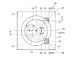
図1は、第1実施形態に係る振動デバイスとしてのヒーター23を搭載した水晶振動子30の概略を示す平面図である。図2は、図1中のA−A断面図である。図1、図2に示すように、水晶振動子30は、パッケージ22、ヒーター23、振動素子21、およびリッド28などを備えている。なお、説明の便宜上、図1ではリッド28の図示を省略している。以下、水晶振動子30の各部について、図1、図2を参照しながら順次説明する。
また、図2において、振動素子21を基準として、リッド28が配置されている方向を上方向、パッケージ22の底板34が配置されている方向を下方向とし、振動素子21、底板34、側壁35の各部材において、上方向に配置されている面を上面、下方向に配置されている面を下面として説明する。
[Crystal oscillator]
FIG. 1 is a plan view illustrating an outline of a
In FIG. 2, the direction in which the
(パッケージ)
まず、パッケージ22について説明する。図2に示すように、パッケージ22は、板状の基板としての底板34と、側壁35と、シームリング40と、パッド電極41と、外部接続電極42などで構成されている。
(package)
First, the
底板34の上面である第1主面51には、振動素子21が、外部接続電極42上に導電性接着剤43を塗布することによって接続されている。一方、第1主面51と反対側、つまり、底板34の下面である第2主面52には、後述するヒーター23や複数のパッド電極41などが設けられている。
外部接続電極42は、第1主面51に2つ設けられており、パッケージ22の底板34に振動素子21を片持ち梁状に固定するための電極である。
The
Two
導電性接着剤43は、接合力を発揮する接着剤成分としての合成樹脂剤に、銀(Ag)製の細粒などの導電性の粒子を含有させたシリコーン系、エポキシ系、またはポリイミド系導電性接着剤などを使用することができる。振動素子21が導電性接着剤43を用いて底板34に接続されている場合には、機械的な固定と電気的な接続とを兼ねさせることができる。
The
側壁35は、第1主面51の表面周縁部に枠状に設けられている。底板34および側壁35は、振動素子21や後述するリッド28の熱膨張係数と一致、あるいは、極力近い熱膨張係数を備えた材料としてセラミックを用いている。具体的には、所定の溶液中にセラミックのパウダーを分散させ、バインダーを添加して生成される混練物がシート状(矩形状)に形成されたセラミックグリーンシートを積層し、焼結することによって形成される。
The
シームリング40は、側壁35の上面に沿って枠状(略矩形状の周状)に、例えば、コバールなどの合金で形成されており、リッド28と側壁35の上面とを接合する部材である。
The
パッド電極41は、図1、図2に示すように、本実施形態では第2主面52の4つの角部にそれぞれ1つずつ設けられている。パッド電極41は、外部接続電極42および外部の基板などと接続されて、水晶振動子30に駆動電圧を供給し、また、水晶振動子30から発振される周波数を外部に出力する電極である。
As shown in FIGS. 1 and 2, one
パッド電極41および外部接続電極42は、例えば、銀(Ag)・パラジウム(Pd)などの導電ペースト、あるいはタングステンメタライズなどを用い、必要とされる形状を形成後に焼成を行い、その後、ニッケル(Ni)および金(Au)あるいは銀(Ag)などをメッキすることによって形成される。
The
(ヒーター)
次に、発熱部としてのヒーター23について、図1、図2を参照しながら説明する。図1、図2に示すように、ヒーター23は、第2主面52に、パッケージ22の平面視にて、振動素子21と重なるように、樹脂接着剤(図示せず)などによって固定されている。
(heater)
Next, the
図2に示すように、ヒーター23は、水晶振動子30を加熱し、温度を一定に保つ、いわゆる恒温機能を有しているパワートランジスターなどの発熱体45、温度センサー46などで構成されている電子部品である。
As shown in FIG. 2, the
さらに、ヒーター23は、ヒーター23の一方の面から延出されている接続部48を備えている。接続部48は、ヒーター23を第2主面52に機械的に固定し、かつ、ヒーター23に電流を供給できるように配線が設けられている。
Further, the
発熱体45は、電流を流すことで熱を発生できるものであればよい。例えば、炭素皮膜抵抗器、金属皮膜抵抗器などの固定抵抗器、可変抵抗器、半固定抵抗器などの抵抗器、白金やその他の導電性素材からなる電気抵抗を有する配線などであって、素子型またはチップ型のものなどが挙げられる。発熱体45は、温度を測定しながら一定の温度に保てるように制御している温度センサー46によって温度コントロールされている。
The
また、ヒーター23と第2主面52との間に、発熱体45に対向するように底板34よりも熱伝導率の高い熱伝導層49が設けられていてもよい。その場合には、熱伝導層49の表面にヒーター23とパッケージ22の底板34とが接触されている。こうすることによって、ヒーター23とパッケージ22とが、熱伝導層49を介して接触する面積が大きくなり、効率よく発熱体45からの熱(熱エネルギー)を水晶振動子30に伝えることができる。従って、パッケージ22に接続されている振動素子21の温度変化が低減されるので、周波数安定性がさらに高くなり、低消費電力化が可能となる。
Further, a heat
(振動素子)
次に、振動素子21について説明する。本実施形態の振動素子21は、圧電材料の一例としての水晶により形成されたATカット水晶基板(圧電基板)が用いられている。図示は省略するが、水晶などの圧電材料は三方晶系に属し、互いに直交する結晶軸X、Y、Zを有する。X軸、Y軸、Z軸は、それぞれ電気軸、機械軸、光学軸と呼称される。そして、水晶基板はXZ面をX軸の回りに所定の角度θだけ回転させた平面に沿って、水晶から切り出された平板が用いられる。
(Vibration element)
Next, the
例えば、ATカット水晶基板の場合は、θは略35°15′である。Y軸、およびZ軸もX軸の回りにθだけ回転させて、それぞれY’軸、およびZ’軸とする。従って、ATカット水晶基板は、直交する結晶軸X、Y’、Z’を有する。ATカット水晶基板は、厚み方向がY’軸であって、Y’軸に直交するXZ’面(X軸、およびZ’軸を含む面)が主面であり、厚みすべり振動が主振動として励振される。 For example, in the case of an AT cut quartz substrate, θ is approximately 35 ° 15 ′. The Y axis and the Z axis are also rotated around the X axis by θ to be the Y ′ axis and the Z ′ axis, respectively. Accordingly, the AT-cut quartz substrate has crystal axes X, Y ′, and Z ′ that are orthogonal to each other. The AT-cut quartz substrate has a thickness direction of the Y ′ axis, the XZ ′ plane (plane including the X axis and the Z ′ axis) orthogonal to the Y ′ axis is the main surface, and the thickness shear vibration is the main vibration. Excited.
このATカット水晶基板を加工して、振動素子21の圧電基板を得ることができる。つまり、圧電基板は、X軸(電気軸)、Y軸(機械軸)、Z軸(光学軸)からなる直交座標系のX軸を中心として、Z軸をY軸の−Y方向へ傾けた軸をZ’軸とし、Y軸をZ軸の+Z方向へ傾けた軸をY’軸とし、X軸とZ’軸に平行な面で構成され、Y’軸に平行な方向を厚みとするATカット水晶基板からなる。
By processing this AT-cut quartz substrate, the piezoelectric substrate of the
振動素子21は、ATカット振動素子に限らず、SCカット振動素子、音叉型振動素子、双音叉型振動素子などを例示することができる。SCカット振動素子とは、先述したZ軸の回りに時計方向に、X軸をα=3°以上30°以下回転させて設定したX’軸に平行な辺を有し、X’軸の回りに時計方向にZ軸をβ=33°以上36°以下回転させたZ’軸に平行な辺を有する、いわゆるダブルローテーションカットである。本実施形態では、α=約22°、β=約34°となっている。
The
振動素子21の種類によって、水晶振動子30のデバイスとしての機能が決定される。例えば、振動素子21が、ATカット振動素子、音叉型振動素子、双音叉型振動素子である場合には、水晶振動子30は、クロックモジュール、あるいは、後述する発振器90などに組み込まれてタイミングデバイスとなる。
The function of the
なお、振動素子21は、図1において、略円形で図示されているが、矩形、六角形、八角形などの多角形、楕円形でも構わない。また、振動素子21は、図2において、両方の面がフラット形状(板形状)で図示されているが、水晶基板の一方の面だけをレンズ状に加工した、小型化に有利なプラノコンベックス形状でもよく、両方の面をレンズ状に加工したバイコンベックス形状であってもよい。
In addition, although the
さらに、振動素子21は、タンタル酸リチウム、ニオブ酸リチウムなどの圧電材料で形成されてもよい。振動素子21が水晶以外の材料で形成される場合には、水晶で形成された場合と同様の振る舞いを生じるように、結晶の方位(カット角)などを選択する。
Furthermore, the
図1、図2に示すように、振動素子21の表面には、励振電極24、および引出電極25が形成されている。励振電極24は、振動素子21に先述した厚みすべり振動を励振させるための電極である。励振電極24は、振動素子21の上下面の中央部に、振動素子21の外形と比較して若干小さく略円形に形成されており、下面の励振電極24は、上面の励振電極24と対向するように形成されている。
As shown in FIGS. 1 and 2, an
引出電極25は、励振電極24とパッケージ22の外部接続電極42とを、例えば、導電性接着剤43を塗布することによって電気的に接続するための電極であり、振動素子21の上下面に配置されている。振動素子21の上面の引出電極25は、上面に配置されている励振電極24の端部から一方の外部接続電極42と重なる振動素子21の端部まで形成されている。また、振動素子21の下面の引出電極25は、下面に配置されている励振電極24の端部から他方の外部接続電極42と重なる振動素子21の端部まで形成されている。
The
(取付け部)
次に、取付け部について説明する。図1、図2に示すように、振動素子21は、第1主面51に配置されている2カ所の外部接続電極42上に導電性接着剤43などを塗布して乾燥することによって、パッケージ22の底板34に片持ち梁状に固定されている。
(Mounting part)
Next, the attachment part will be described. As shown in FIG. 1 and FIG. 2, the
振動素子21が固定されている2カ所のうち、上面の励振電極24(引出電極25)と接続されている一方を第1取付け部26、下面の励振電極24(引出電極25)と接続されている他方を第2取付け部27と言う。
Of the two places where the
第1取付け部26においては、外部接続電極42と、振動素子21の上面に形成されている励振電極24と、の間で導通を取るため、外部接続電極42に導電性接着剤43を塗布し、振動素子21の端部が、塗布した導電性接着剤43と重なるように振動素子21を搭載して、さらに、その上から導電性接着剤43を塗布する。
In the first mounting
第2取付け部27においては、外部接続電極42と、振動素子21の下面に形成されている励振電極24と、の間で導通を取るため、外部接続電極42に導電性接着剤43を塗布し、振動素子21の端部が、塗布した導電性接着剤43と重なるように振動素子21を搭載すればよく、第1取付け部26のように、その上から導電性接着剤43を塗布しなくてもよい。
In the
なお、振動素子21の固定方法としては、底板34の外部接続電極42に金属で形成されるバンプによるバンプ接合であってもよい。
The
図1に示すように、パッケージ22の平面視にて、ヒーターの中心部33と振動素子の中心部31とを結ぶ線を仮想線としての仮想中心線38とすると、仮想中心線38に対して、第1取付け部26と第2取付け部27とが略線対称の位置に配置されている。
また、ヒーターの中心部33は、振動素子の中心部31に対して、第1取付け部26および第2取付け部27と反対側に配置されている。
As shown in FIG. 1, when a line connecting the
Further, the
ここで、振動素子の中心部31と第1取付け部の中心部36とを結ぶ第1中心線56と、仮想中心線38と、がなす角をθ1とする。また、振動素子の中心部31と第2取付け部の中心部37とを結ぶ第2中心線57と、仮想中心線38と、がなす角をθ2とする。
そのとき、0°<θ1<90°、かつ、0°<θ2<90°、かつ、0°<|θ1−θ2|<10°となっている。
Here, an angle formed by the
At that time, 0 ° <θ 1 <90 °, 0 ° <θ 2 <90 °, and 0 ° <| θ 1 −θ 2 | <10 °.
このような構成にすることによって、第1取付け部26と第2取付け部27との距離を短くできる。さらに、パッケージ22の平面視にて、仮想中心線38に対して、第1取付け部26と第2取付け部27とが略線対称の位置に配置されているため、乾燥時やリフロー時などの製造上の熱処理工程において、振動素子21と底板34の熱膨張係数の違いから発生する熱応力(面内応力)が振動素子21に与える影響を低減することができる。従って、水晶振動子30の発振周波数の変動を低減することができる。
By adopting such a configuration, the distance between the first mounting
次に、θ1、およびθ2が、0°<θ1<30°、かつ、0°<θ2<30°を満足している場合について、さらに、0°<θ1<15°、かつ、0°<θ2<15°を満足している場合について、図3を参照しながら説明する。 Next, in the case where θ 1 and θ 2 satisfy 0 ° <θ 1 <30 ° and 0 ° <θ 2 <30 °, 0 ° <θ 1 <15 ° and , 0 ° <θ 2 <15 ° will be described with reference to FIG.
図3は、第1実施形態に係る振動素子の中心部31と第1取付け部の中心部36とを結ぶ第1中心線56と、仮想中心線38と、がなす角θ1、(あるいは、振動素子の中心部31と第2取付け部の中心部37とを結ぶ第2中心線57と、仮想中心線38と、がなす角θ2)と、熱応力による発振周波数の変化量Δf/fと、の関係を示す図である。
3 shows an angle θ 1 formed by a
図3は、θ=θ1、θ2をパラメーター(横軸)として、水晶振動子30の周囲温度を+85℃から−40℃に変化させた時に発生する熱応力による発振周波数の変化をFEM(Finite Element Method)によって計算されたものである。縦軸は規格化された周波数偏差をΔF/F[ppm]で示している。
FIG. 3 shows changes in the oscillation frequency due to thermal stress generated when the ambient temperature of the
θ1,θ2が、0°<|θ1−θ2|<10°を満足していることから、仮想中心線38に対して、第1取付け部26と第2取付け部27とが略線対称の位置に配置されている。
Since θ 1 and θ 2 satisfy 0 ° <| θ 1 −θ 2 | <10 °, the first mounting
まず、0°<θ1<30°、かつ、0°<θ2<30°である場合には、第1取付け部26と第2取付け部27との距離をさらに短くできる。図3に示すように、θが0°<θ<30°を満足している場合には、30°≦θの場合と比較して、熱応力による発振周波数の変化量がさらに小さくなっている。つまり、乾燥時、リフロー時などの熱処理工程において、振動素子21とパッケージ22との熱膨張係数の違いによって発生する熱応力をさらに低減することができる。
First, when 0 ° <θ 1 <30 ° and 0 ° <θ 2 <30 °, the distance between the first mounting
次に、0°<θ1<15°、かつ、0°<θ2<15°である場合には、第1取付け部26と第2取付け部27との距離をさらに短くできる。図3に示すように、θが0°<θ<15°を満足している場合には、15°≦θの場合と比較して、熱応力による発振周波数の変化量がさらに小さくなっている。つまり、乾燥時、リフロー時などの熱処理工程において、振動素子21とパッケージ22との熱膨張係数の違いによって発生する熱応力をさらに低減することができる。
Next, when 0 ° <θ 1 <15 ° and 0 ° <θ 2 <15 °, the distance between the first mounting
(リッド)
次に、リッド28は、板状の部材であるため形成しやすく、形状の安定にも優れており、セラミック、金属、ガラスなどで形成されている。リッド28が、例えば、コバール(金属)で形成されている場合には、一般に他の材料よりも強度が高い利点がある。また、リッド28に板状のコバールを用いることによって、封止の際にコバールで形成されているシームリング40とリッド28とが同じ溶融状態で溶融され、合金化もされやすいため封止を容易に、かつ確実に行うことができる。
(Lid)
Next, since the
なお、リッド28は、コバールに限らず他の材料を用いてもよい。例えば、42アロイ、ステンレス鋼などの金属材料、またはパッケージ22の側壁35と同材料(例えば、セラミック)などを用いることができる。
The
そして、シーム溶接法などを用いてシームリング40を溶融し、図2に示すように、パッケージ22とリッド28とを接合することによって、パッケージ22の底板34と側壁35とに囲まれている凹部の開口が塞がれて、振動素子21などを収納するための密閉された内部空間29が形成される。
Then, the
内部空間29は、その内部圧力を所望の気圧に設定できる。例えば、内部空間29は窒素ガスを充填して大気圧にしたり、通常の大気圧より低い圧力(1×10⁵Pa〜1×10⁻¹⁰Pa以下(JIS Z 8126‐1:1999))の状態(以下、真空と言う)にしたりすることができる。
The
本実施形態の内部空間29は真空に設定されている。内部空間29を真空にすると、水晶振動子30のQ値を高められるので発振周波数が安定し、かつ、外部への熱の流出を低減することができるため、低消費電力化することが可能となる。
The
[発振器]
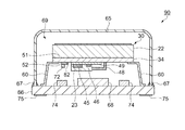
次に、本実施形態の水晶振動子30を搭載した発振器90について図4を参照しながら説明する。図4は、第1実施形態に係る振動デバイスとしてのヒーター23を搭載した水晶振動子30を適用した発振器90の概略を示す断面図である。図4に示すように、発振器90は、ヒーター23、およびICチップ(チップ部品)72を搭載した水晶振動子30と、脚部60と、ケース65と、ベース66と、回路素子68と、他の回路構成部品74などで構成されている。
[Oscillator]
Next, an
水晶振動子30の第2主面52には、ヒーター23の他に、脚部60が接続されており、さらに、ICチップ72がろう材あるいは接着剤などの接合部材82を介して固定されている。ICチップ72は、水晶振動子30の駆動を制御するための駆動回路(発振回路)を有しており、このICチップ72によって水晶振動子30を駆動して外部に周波数を取り出すことができる。また、他の回路構成部品74とは、抵抗、コイル、コンデンサーなどを組み合わせて構成されている電子部品である。
In addition to the
(脚部)
脚部60は、水晶振動子30とベース66とが2段構造になるように固定する部材である。つまり、脚部60によって、水晶振動子30に固定されているヒーター23から発生する熱が、後述する回路素子68などが搭載されているベース66に伝わり難い構造になっている。このような構造にすることによって、回路素子68などがヒーター23によって高温にさらされることが低減され、発振器90は、安定した周波数を発振することが可能となる。
(leg)
The
また、脚部60は水晶振動子30とベース66とを電気的に接続できるように、導電性を有する金属フレームで構成されている。脚部60の材料として、例えば、リードフレームの材料を挙げることができる。つまり、脚部60は、Cu系素材(Cu‐Fe‐Pなど)、Fe系素材(Fe‐42%Niなど)、その他の機械的強度、電気伝導度、熱伝導度、耐食性などに優れた金属素材の薄板が使用される。さらに、脚部60の表面には、Au、Ag、Sn、Pd、半田などのめっきが施されていてもよい。
Further, the
(ケース)
次に、ケース65は、振動素子21を収納しているパッケージ22、ヒーター23、などを収納することができる凹状の容器である。ケース65の平面的な形状は、矩形に限らず、多角形、円形、楕円形などの形状であってもよい。ケース65は、振動素子21およびヒーター23をケース65の内部に導入することができる程度の開口を備えており、ケース65は、セラミック、ガラスなどの無機材料、樹脂またはコバールなどの金属材料で形成されている。
(Case)
Next, the
(ベース)
ベース66は、ケース65の開口を封止する平板形状を有している。ベース66の形状としては、特に限定されず、外部から底板34への接触を避ける程度の形状、または、ケース65の開口を封止して密閉空間を形成することができる形状とすることができる。ベース66は、例えば、セラミック、ガラス、金属などで形成することができ、本実施形態では、コバール(金属)で形成されている。
(base)
The
ベース66の、脚部60が接続されている側の面(内面)には、後述する回路素子68、他の回路構成部品74などが設けられており、ベース66の、脚部60が接続されている側とは反対の面(外面)には、外部接続端子75などが設けられている。外部接続端子75は、回路素子68、他の回路構成部品74などと電気的に接続されている。また、ベース66は、脚部60を介してヒーター23に電気的に接続するための配線を備えている。
On the surface (inner surface) of the base 66 on the side to which the
ベース66とベース66に被せられたケース65とが、半田67などを用いて接着されることによって、内部空間69が形成される。ベース66とケース65との接着は、半田67の他に、例えば、プラズマ溶接、シーム溶接、超音波接合、または接着剤などを用いても行われることができる。
The
内部空間69は、振動素子21、ヒーター23、回路素子68、ICチップ72などが収納されている空間である。内部空間69は、大気開放されていてもよいし、気密空間であってもよい。内部空間69が気密空間の場合には、振動素子21、ヒーター23を減圧状態や不活性ガス雰囲気にすることもできる。本実施形態では、内部空間69は略真空の減圧状態となっており、ヒーター23の加熱におけるエネルギー効率を高めることができる。
The
(回路素子)
次に、回路素子68は、ベース66上に導電性接着剤(図示せず)などによって接続されている。回路素子68は、例えば、水晶振動子30の振動素子21を発振させる発振回路、あるいはヒーター23の温度制御を行う制御回路などを備えている。
(Circuit element)
Next, the
<変形例>
次に、第1実施形態の変形例に係る水晶振動子130について図5を参照して説明する。なお、上記第1実施形態との共通部分については、同一符号を付して説明を省略し、上記第1実施形態と異なる部分を中心に説明する。
<Modification>
Next, a
[水晶振動子]
図5は、第1実施形態の変形例に係る振動デバイスとしてのヒーターを搭載した水晶振動子130の概略を示す平面図である。図5に示すように、水晶振動子130は、上記の第1実施形態の水晶振動子30と比較して、振動素子21とヒーター23との相対位置が異なるものである。
[Crystal oscillator]
FIG. 5 is a plan view illustrating an outline of a
第1実施形態と同様に、変形例に係る振動素子21は、パッケージ22の底板34の第1主面51に配置されている第1取付け部26、第2取付け部27の2カ所において、外部接続電極42上に導電性接着剤43などを塗布することによって、外部接続電極42に片持ち梁状に取付けられ、固定されている。
Similar to the first embodiment, the
また、第1実施形態と同様に、パッケージ22の平面視にて、ヒーターの中心部33と振動素子の中心部31とを結ぶ線を仮想線としての仮想中心線38とすると、仮想中心線38に対して、第1取付け部26と第2取付け部27とが線対称の位置に配置されている。
Similarly to the first embodiment, when a line connecting the
しかし、第1実施形態と異なり、振動素子の中心部31に対して、ヒーターの中心部33と、第1取付け部26と、が同じ側に配置されており、ヒーターの中心部33と、第2取付け部27と、が同じ側に配置されている。
However, unlike the first embodiment, the
このような構成にすることによって、ヒーター23からパッケージ22の底板34に配置されている第1取付け部26、第2取付け部27を介して振動素子21までの距離が短縮される。従って、ヒーター23から発生する熱が振動素子21に伝わりやすくなるため、振動素子21の温度変化が低減され、水晶振動子130の発振周波数が安定する。また、伝熱経路にて熱の損失が低減されるため、低消費電力化が可能となる。
With such a configuration, the distance from the
<第2実施形態>
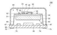
次に、第2実施形態に係る発振器190について図6を参照して説明する。なお、前述の第1実施形態に係る発振器90と同様な構成については同符号を付して説明を省略する。
Second Embodiment
Next, an
[発振器]
図6は、第2実施形態に係る振動デバイスとしてのヒーター23を搭載した水晶振動子30を適用した発振器190の概略を示す断面図である。図6に示すように、発振器190は、ヒーター23、およびICチップ(チップ部品)72を搭載した水晶振動子30と、脚部60と、ケース65と、ベース66と、回路素子68と、他の回路構成部品74などで構成されている。構成されている部品は、第1実施形態と同じである。
[Oscillator]
FIG. 6 is a cross-sectional view schematically illustrating an
しかし、第2実施形態において、ヒーター23は、水晶振動子30に対して、ベース66とは反対側に配置されている。つまり、発振器190は、水晶振動子30を上下反転させて固定されている構造であることが第1実施形態と異なる。
However, in the second embodiment, the
このような構成にすることによって、第2実施形態における発振器190においても、前述した第1実施形態に係る発振器90と同様な効果を得ることができる。さらに、ヒーター23と、ベース66上に配置されている回路素子68や他の回路構成部品74などと、の距離が第1実施形態と比較して長くなることから、回路素子68や他の回路構成部品74などがヒーター23によって高温にさらされることを低減させることが可能になる。
By adopting such a configuration, the same effect as that of the
[電子機器]
次いで、本発明の実施形態に係る振動デバイスとしての水晶振動子30(または水晶振動子130、以下は水晶振動子30にて説明する)を適用した電子機器について、図7〜図9に基づき、詳細に説明する。
[Electronics]
Next, based on FIGS. 7 to 9, an electronic apparatus to which the crystal resonator 30 (or the
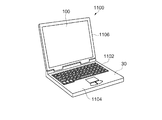
図7は、電子機器の一例としてのモバイル型のパーソナルコンピューターの構成を示す斜視図である。この図において、パーソナルコンピューター1100は、キーボード1102を備えた本体部1104と、表示部100を備えた表示ユニット1106とにより構成され、表示ユニット1106は、本体部1104に対しヒンジ構造部を介して回動可能に支持されている。このようなパーソナルコンピューター1100には、信号処理のタイミング源としての機能を備えた水晶振動子30が内蔵されている。
FIG. 7 is a perspective view illustrating a configuration of a mobile personal computer as an example of an electronic apparatus. In this figure, a
図8は、電子機器の一例としての携帯電話機の構成を示す斜視図である。この図において、携帯電話機1200(PHSも含む)は、複数の操作ボタン1202、受話口1204および送話口1206を備え、操作ボタン1202と受話口1204との間には、表示部100が配置されている。このような携帯電話機1200には、信号処理のタイミング源としての機能を備えた水晶振動子30が内蔵されている。
FIG. 8 is a perspective view illustrating a configuration of a mobile phone as an example of an electronic device. In this figure, a cellular phone 1200 (including PHS) includes a plurality of
図9は、電子機器の一例としてのデジタルスチールカメラの構成を示す斜視図である。なお、この図には、外部機器との接続についても簡易的に示されている。ここで、従来のフィルムカメラは、被写体の光像により銀塩写真フィルムを感光するのに対し、デジタルスチールカメラ1300は、被写体の光像をCCD(Charge Coupled Device)などの撮像素子により光電変換して撮像信号(画像信号)を生成する。
FIG. 9 is a perspective view illustrating a configuration of a digital still camera as an example of an electronic apparatus. In this figure, connection with an external device is also simply shown. Here, the conventional film camera sensitizes the silver halide photographic film with the light image of the subject, whereas the
デジタルスチールカメラ1300におけるケース(ボディー)1302の背面には、表示部100が設けられ、CCDによる撮像信号に基づいて表示を行う構成になっており、表示部100は、被写体を電子画像として表示するファインダーとして機能する。また、ケース1302の正面側(図中裏面側)には、光学レンズ(撮像光学系)やCCDなどを含む受光ユニット1304が設けられている。
A
撮影者が表示部100に表示された被写体像を確認し、シャッターボタン1306を押下すると、その時点におけるCCDの撮像信号が、メモリー1308に転送、格納される。また、このデジタルスチールカメラ1300においては、ケース1302の側面に、ビデオ信号出力端子1312と、データ通信用の入出力端子1314とが設けられている。
When the photographer confirms the subject image displayed on the
そして、図示されるように、ビデオ信号出力端子1312にはテレビモニター1430が、データ通信用の入出力端子1314にはパーソナルコンピューター1440が、それぞれ必要に応じて接続される。さらに、所定の操作により、メモリー1308に格納された撮像信号が、テレビモニター1430や、パーソナルコンピューター1440に出力される構成になっている。このようなデジタルスチールカメラ1300には、信号処理のタイミング源としての機能を備えた水晶振動子30が内蔵されている。
As shown in the figure, a
なお、本発明の実施形態に係る水晶振動子30を備える電子機器は、図7のパーソナルコンピューター1100(モバイル型パーソナルコンピューター)、図8の携帯電話機1200、図9のデジタルスチールカメラ1300の他にも、例えば、インクジェット式吐出装置(例えば、インクジェットプリンター)、ラップトップ型パーソナルコンピューター、テレビ、ビデオカメラ、ビデオテープレコーダー、カーナビゲーション装置、ページャー、電子手帳(通信機能付も含む)、電子辞書、電卓、電子ゲーム機器、ワードプロセッサー、ワークステーション、テレビ電話、防犯用テレビモニター、電子双眼鏡、POS端末、医療機器(例えば、電子体温計、血圧計、血糖計、心電図計測装置、超音波診断装置、電子内視鏡)、魚群探知機、各種測定機器、計器類(例えば、車両、航空機、船舶の計器類)、フライトシミュレーターなどの電子機器、移動体通信基地局用機器、ルーターやスイッチなどのストレージエリアネットワーク機器、ローカルエリアネットワーク機器、ネットワーク用伝送機器などに適用することができる。
Note that the electronic device including the
[移動体]
図10は移動体の一例としての自動車1500を概略的に示す斜視図である。自動車1500には本発明に係る水晶振動子30が搭載されている。例えば、同図に示すように、移動体としての自動車1500には、水晶振動子30を内蔵してタイヤ1503などを制御する電子制御ユニット1510が車体1501に搭載されている。
[Moving object]
FIG. 10 is a perspective view schematically showing an
また、水晶振動子30は、他にもキーレスエントリー、イモビライザー、カーナビゲーションシステム、カーエアコン、アンチロックブレーキシステム(ABS:Antilock Brake System)、エアバック、タイヤ・プレッシャー・モニタリング・システム(TPMS:Tire Pressure Monitoring System)、エンジンコントロール、ハイブリッド自動車や電気自動車の電池モニター、車体姿勢制御システム、などの電子制御ユニット(ECU:Electronic Control Unit)に広く適用できる。
In addition, the
以上、本発明の振動子、発振器、電子機器および移動体の実施形態について、図面に基づいて説明したが、本発明は、上記実施形態に限定されるものではなく、各部の構成は、同様の機能を有する任意の構成のものに置換することができる。また、本発明に、他の任意の構成物が付加されていてもよい。また、各実施形態を適宜組み合わせてもよい。 As described above, the embodiments of the vibrator, the oscillator, the electronic device, and the moving body of the present invention have been described based on the drawings. However, the present invention is not limited to the above-described embodiment, and the configuration of each part is the same. Any structure having a function can be substituted. In addition, any other component may be added to the present invention. Moreover, you may combine each embodiment suitably.
21…振動素子、22…パッケージ、23…ヒーター、24…励振電極、25…引出電極、26…第1取付け部、27…第2取付け部、28…リッド、29…内部空間、30…水晶振動子、31…振動素子の中心部、33…ヒーターの中心部、34…底板、35…側壁、36…第1取付け部の中心部、37…第2取付け部の中心部、38…仮想中心線、40…シームリング、41…パッド電極、42…外部接続電極、43…導電性接着剤、45…発熱体、46…温度センサー、48…接続部、49…熱伝導層、51…第1主面、52…第2主面、56…第1中心線、57…第2中心線、60…脚部、65…ケース、66…ベース、67…半田、68…回路素子、69…内部空間、72…ICチップ、74…他の回路構成部品、75…外部接続端子、82…接合部材、90…発振器、100…表示部、130…水晶振動子、190…発振器、1100…パーソナルコンピューター、1102…キーボード、1104…本体部、1106…表示ユニット、1200…携帯電話機、1202…操作ボタン、1204…受話口、1206…送話口、1300…デジタルスチールカメラ、1302…ケース、1304…受光ユニット、1306…シャッターボタン、1308…メモリー、1312…ビデオ信号出力端子、1314…入出力端子、1430…テレビモニター、1440…パーソナルコンピューター、1500…自動車、1501…車体、1503…タイヤ、1510…電子制御ユニット。
DESCRIPTION OF
Claims (6)
前記基板の第1主面に、第1取付け部および第2取付け部にて取付けられている振動素子と、
前記第1主面とは反対側の第2主面に、平面視で前記振動素子と重なるように配置されている発熱部と、
を含み、
平面視で、前記発熱部の中心部と前記振動素子の中心部とを結ぶ仮想線に対し、
前記振動素子の中心部と前記第1取付け部の中心部とを結ぶ線とがなす角をθ1、
前記振動素子の中心部と前記第2取付け部の中心部とを結ぶ線とがなす角をθ2としたとき、
0°<θ1<90°、かつ、0°<θ2<90°、かつ、0°<|θ1−θ2|<10°を満足していることを特徴とする振動デバイス。 A substrate,
A vibration element attached to the first main surface of the substrate by a first attachment portion and a second attachment portion;
A heat generating portion disposed on the second main surface opposite to the first main surface so as to overlap the vibration element in plan view;
Including
In a plan view, with respect to an imaginary line connecting the central portion of the heat generating portion and the central portion of the vibration element,
An angle formed by a line connecting the center portion of the vibration element and the center portion of the first mounting portion is θ 1 ,
When the angle formed by the line connecting the center portion of the vibration element and the center portion of the second mounting portion is θ 2 ,
A vibration device characterized by satisfying 0 ° <θ 1 <90 °, 0 ° <θ 2 <90 °, and 0 ° <| θ 1 −θ 2 | <10 °.
0°<θ1<30°、かつ、0°<θ2<30°を満足していることを特徴とする振動デバイス。 In claim 1,
A vibration device characterized by satisfying 0 ° <θ 1 <30 ° and 0 ° <θ 2 <30 °.
0°<θ1<15°、かつ、0°<θ2<15°を満足していることを特徴とする振動デバイス。 In Claim 1 or Claim 2,
A vibration device characterized by satisfying 0 ° <θ 1 <15 ° and 0 ° <θ 2 <15 °.
Priority Applications (2)
| Application Number | Priority Date | Filing Date | Title |
|---|---|---|---|
| JP2015003924A JP2016131266A (en) | 2015-01-13 | 2015-01-13 | Oscillation device, oscillator, electronic apparatus and mobile body |
| US14/990,247 US9590585B2 (en) | 2015-01-13 | 2016-01-07 | Resonation device, oscillator, electronic apparatus, and moving object |
Applications Claiming Priority (1)
| Application Number | Priority Date | Filing Date | Title |
|---|---|---|---|
| JP2015003924A JP2016131266A (en) | 2015-01-13 | 2015-01-13 | Oscillation device, oscillator, electronic apparatus and mobile body |
Publications (2)
| Publication Number | Publication Date |
|---|---|
| JP2016131266A true JP2016131266A (en) | 2016-07-21 |
| JP2016131266A5 JP2016131266A5 (en) | 2018-02-01 |
Family
ID=56368248
Family Applications (1)
| Application Number | Title | Priority Date | Filing Date |
|---|---|---|---|
| JP2015003924A Withdrawn JP2016131266A (en) | 2015-01-13 | 2015-01-13 | Oscillation device, oscillator, electronic apparatus and mobile body |
Country Status (2)
| Country | Link |
|---|---|
| US (1) | US9590585B2 (en) |
| JP (1) | JP2016131266A (en) |
Families Citing this family (2)
| Publication number | Priority date | Publication date | Assignee | Title |
|---|---|---|---|---|
| JP5747574B2 (en) | 2011-03-11 | 2015-07-15 | セイコーエプソン株式会社 | Piezoelectric device and electronic equipment |
| EP4032185A4 (en) * | 2019-09-16 | 2023-11-08 | Rakon Limited | Doubly rotated quartz crystal resonators with reduced sensitivity to acceleration |
Citations (3)
| Publication number | Priority date | Publication date | Assignee | Title |
|---|---|---|---|---|
| JPS51110292A (en) * | 1975-03-24 | 1976-09-29 | Nippon Electric Co | ATSUDENSHINDOSHI |
| JP2014236398A (en) * | 2013-06-04 | 2014-12-15 | セイコーエプソン株式会社 | Oscillating device, electronic apparatus, and moving body |
| JP2015005882A (en) * | 2013-06-21 | 2015-01-08 | 日本電波工業株式会社 | Crystal device |
Family Cites Families (6)
| Publication number | Priority date | Publication date | Assignee | Title |
|---|---|---|---|---|
| JPH10294618A (en) | 1997-04-18 | 1998-11-04 | Toyo Commun Equip Co Ltd | Highly stable crystal oscillator having thermostatic structure |
| US6501340B1 (en) * | 2002-02-11 | 2002-12-31 | Acr Electronics, Inc. | Oscillator with frequency stabilizing circuit and method of constructing same |
| JP2006080180A (en) | 2004-09-08 | 2006-03-23 | Seiko Epson Corp | Electronic component, piezo-electric oscillator and electronic instrument |
| JP5308879B2 (en) * | 2009-03-13 | 2013-10-09 | 日本電波工業株式会社 | Constant temperature crystal oscillator |
| JP5387842B2 (en) | 2009-05-14 | 2014-01-15 | セイコーエプソン株式会社 | Piezoelectric device |
| CN102916672A (en) * | 2012-11-06 | 2013-02-06 | 广东大普通信技术有限公司 | Constant temperature control crystal oscillator and manufacturing method thereof |
-
2015
- 2015-01-13 JP JP2015003924A patent/JP2016131266A/en not_active Withdrawn
-
2016
- 2016-01-07 US US14/990,247 patent/US9590585B2/en active Active
Patent Citations (3)
| Publication number | Priority date | Publication date | Assignee | Title |
|---|---|---|---|---|
| JPS51110292A (en) * | 1975-03-24 | 1976-09-29 | Nippon Electric Co | ATSUDENSHINDOSHI |
| JP2014236398A (en) * | 2013-06-04 | 2014-12-15 | セイコーエプソン株式会社 | Oscillating device, electronic apparatus, and moving body |
| JP2015005882A (en) * | 2013-06-21 | 2015-01-08 | 日本電波工業株式会社 | Crystal device |
Also Published As
| Publication number | Publication date |
|---|---|
| US20160204759A1 (en) | 2016-07-14 |
| US9590585B2 (en) | 2017-03-07 |
Similar Documents
| Publication | Publication Date | Title |
|---|---|---|
| US9893733B2 (en) | Oscillator, electronic apparatus, and moving object | |
| JP6098377B2 (en) | Oscillator, electronic device, and moving object | |
| JP6286884B2 (en) | Electronic devices, electronic devices, and moving objects | |
| JP6641859B2 (en) | Vibration devices, oscillators, electronics, and moving objects | |
| JP6596810B2 (en) | Electronic component, method for manufacturing electronic component, electronic device, and moving object | |
| JP6179155B2 (en) | Vibration device, electronic device, and moving object | |
| JP2014110369A (en) | Base substrate, vibrator, oscillator, sensor, electronic device, electronic equipment, and mobile object | |
| TW201351878A (en) | Vibrator element, vibrator, electronic device, electronic apparatus, and mobile object | |
| JP2016029762A (en) | Vibration element, vibrator, oscillator, electronic apparatus and mobile body | |
| JP6740572B2 (en) | Electronic device, electronic device, and base station device | |
| US20160254798A1 (en) | Electronic component, oscillator, electronic apparatus, and moving object | |
| JP6724308B2 (en) | Oscillation module, vibrating device, electronic equipment, and moving body | |
| CN105306001B (en) | Electronic component, method for manufacturing electronic component, electronic apparatus, and moving object | |
| JP2014053663A (en) | Electronic device, electronic apparatus, and moving body | |
| US9590585B2 (en) | Resonation device, oscillator, electronic apparatus, and moving object | |
| JP2014197732A (en) | Vibrator, oscillator, electronic apparatus, and mobile body | |
| JP6729643B2 (en) | Oscillators, electronic devices and mobiles | |
| JP6349722B2 (en) | Vibration device, electronic device, and moving object | |
| JP2017079390A (en) | Vibration element, oscillator, electronic apparatus, mobile body, and base station | |
| JP2015070588A (en) | Vibration element, vibrator, electronic device, electronic apparatus and moving body | |
| JP6634678B2 (en) | Transducers, oscillators, electronic devices, and moving objects | |
| JP2018110447A (en) | Oscillation element, oscillator, electronic device, electronic apparatus and mobile object | |
| JP6572985B2 (en) | Electronic components, crystal oscillators with thermostatic chambers, electronic devices, and moving objects | |
| JP2016174201A (en) | Vibration piece, vibrator, vibration device, oscillator, electronic apparatus, and mobile | |
| JP2016131279A (en) | Vibrator, oscillator, electronic apparatus and mobile object |
Legal Events
| Date | Code | Title | Description |
|---|---|---|---|
| A521 | Request for written amendment filed |
Free format text: JAPANESE INTERMEDIATE CODE: A523 Effective date: 20171212 |
|
| A621 | Written request for application examination |
Free format text: JAPANESE INTERMEDIATE CODE: A621 Effective date: 20171212 |
|
| RD05 | Notification of revocation of power of attorney |
Free format text: JAPANESE INTERMEDIATE CODE: A7425 Effective date: 20180904 |
|
| A977 | Report on retrieval |
Free format text: JAPANESE INTERMEDIATE CODE: A971007 Effective date: 20181012 |
|
| A131 | Notification of reasons for refusal |
Free format text: JAPANESE INTERMEDIATE CODE: A131 Effective date: 20181023 |
|
| RD03 | Notification of appointment of power of attorney |
Free format text: JAPANESE INTERMEDIATE CODE: A7423 Effective date: 20181107 |
|
| A521 | Request for written amendment filed |
Free format text: JAPANESE INTERMEDIATE CODE: A523 Effective date: 20181205 |
|
| A131 | Notification of reasons for refusal |
Free format text: JAPANESE INTERMEDIATE CODE: A131 Effective date: 20190507 |
|
| A761 | Written withdrawal of application |
Free format text: JAPANESE INTERMEDIATE CODE: A761 Effective date: 20190708 |