JP2016100172A - Light-emitting device and method for manufacturing light-emitting device - Google Patents
Light-emitting device and method for manufacturing light-emitting device Download PDFInfo
- Publication number
- JP2016100172A JP2016100172A JP2014235863A JP2014235863A JP2016100172A JP 2016100172 A JP2016100172 A JP 2016100172A JP 2014235863 A JP2014235863 A JP 2014235863A JP 2014235863 A JP2014235863 A JP 2014235863A JP 2016100172 A JP2016100172 A JP 2016100172A
- Authority
- JP
- Japan
- Prior art keywords
- layer
- terminal
- emitting device
- substrate
- electrode
- Prior art date
- Legal status (The legal status is an assumption and is not a legal conclusion. Google has not performed a legal analysis and makes no representation as to the accuracy of the status listed.)
- Pending
Links
- 238000000034 method Methods 0.000 title claims description 24
- 238000004519 manufacturing process Methods 0.000 title claims description 7
- 239000010410 layer Substances 0.000 claims abstract description 155
- 239000000758 substrate Substances 0.000 claims abstract description 58
- 239000002344 surface layer Substances 0.000 claims abstract description 5
- 239000011347 resin Substances 0.000 claims description 18
- 229920005989 resin Polymers 0.000 claims description 18
- 239000004020 conductor Substances 0.000 claims description 16
- 238000004544 sputter deposition Methods 0.000 claims description 11
- 239000000463 material Substances 0.000 claims description 9
- 239000011521 glass Substances 0.000 claims description 5
- 239000012044 organic layer Substances 0.000 description 24
- 238000005192 partition Methods 0.000 description 17
- 229910052751 metal Inorganic materials 0.000 description 10
- 239000002184 metal Substances 0.000 description 10
- 238000003825 pressing Methods 0.000 description 10
- 239000002245 particle Substances 0.000 description 9
- 238000007789 sealing Methods 0.000 description 8
- XLOMVQKBTHCTTD-UHFFFAOYSA-N Zinc monoxide Chemical compound [Zn]=O XLOMVQKBTHCTTD-UHFFFAOYSA-N 0.000 description 4
- 238000002347 injection Methods 0.000 description 4
- 239000007924 injection Substances 0.000 description 4
- 229920001721 polyimide Polymers 0.000 description 4
- 238000007740 vapor deposition Methods 0.000 description 4
- 229910052782 aluminium Inorganic materials 0.000 description 3
- 238000000576 coating method Methods 0.000 description 3
- 238000009751 slip forming Methods 0.000 description 3
- 229910001182 Mo alloy Inorganic materials 0.000 description 2
- 239000004695 Polyether sulfone Substances 0.000 description 2
- 239000004642 Polyimide Substances 0.000 description 2
- VYPSYNLAJGMNEJ-UHFFFAOYSA-N Silicium dioxide Chemical compound O=[Si]=O VYPSYNLAJGMNEJ-UHFFFAOYSA-N 0.000 description 2
- 238000002441 X-ray diffraction Methods 0.000 description 2
- 238000000231 atomic layer deposition Methods 0.000 description 2
- 238000005229 chemical vapour deposition Methods 0.000 description 2
- 238000002788 crimping Methods 0.000 description 2
- 239000002274 desiccant Substances 0.000 description 2
- 238000010586 diagram Methods 0.000 description 2
- 238000001704 evaporation Methods 0.000 description 2
- 229910052737 gold Inorganic materials 0.000 description 2
- 239000010931 gold Substances 0.000 description 2
- 230000005525 hole transport Effects 0.000 description 2
- 239000004973 liquid crystal related substance Substances 0.000 description 2
- 239000011159 matrix material Substances 0.000 description 2
- 239000012528 membrane Substances 0.000 description 2
- 229910052750 molybdenum Inorganic materials 0.000 description 2
- 238000000206 photolithography Methods 0.000 description 2
- 229920003207 poly(ethylene-2,6-naphthalate) Polymers 0.000 description 2
- 229920006393 polyether sulfone Polymers 0.000 description 2
- -1 polyethylene naphthalate Polymers 0.000 description 2
- 239000011112 polyethylene naphthalate Substances 0.000 description 2
- 229920000139 polyethylene terephthalate Polymers 0.000 description 2
- 239000005020 polyethylene terephthalate Substances 0.000 description 2
- 239000009719 polyimide resin Substances 0.000 description 2
- 230000001681 protective effect Effects 0.000 description 2
- 238000005001 rutherford backscattering spectroscopy Methods 0.000 description 2
- 239000011787 zinc oxide Substances 0.000 description 2
- 239000004925 Acrylic resin Substances 0.000 description 1
- 229920000178 Acrylic resin Polymers 0.000 description 1
- 229910000838 Al alloy Inorganic materials 0.000 description 1
- OKTJSMMVPCPJKN-UHFFFAOYSA-N Carbon Chemical compound [C] OKTJSMMVPCPJKN-UHFFFAOYSA-N 0.000 description 1
- 229920001609 Poly(3,4-ethylenedioxythiophene) Polymers 0.000 description 1
- BSUHXFDAHXCSQL-UHFFFAOYSA-N [Zn+2].[W+4].[O-2].[In+3] Chemical compound [Zn+2].[W+4].[O-2].[In+3] BSUHXFDAHXCSQL-UHFFFAOYSA-N 0.000 description 1
- 239000000853 adhesive Substances 0.000 description 1
- 230000001070 adhesive effect Effects 0.000 description 1
- 229910045601 alloy Inorganic materials 0.000 description 1
- 239000000956 alloy Substances 0.000 description 1
- XAGFODPZIPBFFR-UHFFFAOYSA-N aluminium Chemical compound [Al] XAGFODPZIPBFFR-UHFFFAOYSA-N 0.000 description 1
- 230000004888 barrier function Effects 0.000 description 1
- 230000015572 biosynthetic process Effects 0.000 description 1
- 239000002041 carbon nanotube Substances 0.000 description 1
- 229910021393 carbon nanotube Inorganic materials 0.000 description 1
- 238000005401 electroluminescence Methods 0.000 description 1
- 239000003822 epoxy resin Substances 0.000 description 1
- PCHJSUWPFVWCPO-UHFFFAOYSA-N gold Chemical compound [Au] PCHJSUWPFVWCPO-UHFFFAOYSA-N 0.000 description 1
- 238000010438 heat treatment Methods 0.000 description 1
- 229910052738 indium Inorganic materials 0.000 description 1
- AMGQUBHHOARCQH-UHFFFAOYSA-N indium;oxotin Chemical compound [In].[Sn]=O AMGQUBHHOARCQH-UHFFFAOYSA-N 0.000 description 1
- 229910010272 inorganic material Inorganic materials 0.000 description 1
- 239000011147 inorganic material Substances 0.000 description 1
- 229910052749 magnesium Inorganic materials 0.000 description 1
- 229910044991 metal oxide Inorganic materials 0.000 description 1
- 150000004706 metal oxides Chemical class 0.000 description 1
- 239000002923 metal particle Substances 0.000 description 1
- 230000003287 optical effect Effects 0.000 description 1
- 239000011368 organic material Substances 0.000 description 1
- 229910052697 platinum Inorganic materials 0.000 description 1
- 229920000647 polyepoxide Polymers 0.000 description 1
- 230000002250 progressing effect Effects 0.000 description 1
- 239000000377 silicon dioxide Substances 0.000 description 1
- 235000012239 silicon dioxide Nutrition 0.000 description 1
- 229910052814 silicon oxide Inorganic materials 0.000 description 1
- 229910052709 silver Inorganic materials 0.000 description 1
- 239000007921 spray Substances 0.000 description 1
- 229910052718 tin Inorganic materials 0.000 description 1
- 239000011800 void material Substances 0.000 description 1
- 230000003313 weakening effect Effects 0.000 description 1
- 229910052725 zinc Inorganic materials 0.000 description 1
- 239000011701 zinc Substances 0.000 description 1
- YVTHLONGBIQYBO-UHFFFAOYSA-N zinc indium(3+) oxygen(2-) Chemical compound [O--].[Zn++].[In+3] YVTHLONGBIQYBO-UHFFFAOYSA-N 0.000 description 1
Images


Abstract
Description
本発明は、発光装置及び発光装置の製造方法に関する。 The present invention relates to a light emitting device and a method for manufacturing the light emitting device.
近年は、発光素子として有機EL(Organic Electroluminescence)素子を有する発光装置の開発が進んでいる。このような発光装置において、有機EL素子は基板に形成されている。この基板には、有機EL素子に接続する端子が設けられている。この端子には、FPC(Flexible Printed circuit)、リード端子、又はボンディングワイヤなどの導通部材が接続されている。端子がFPCに接続する場合、端子とFPCは異方性導電性膜を介して互いに接続する場合が多い。 In recent years, development of light-emitting devices having organic EL (Organic Electroluminescence) elements as light-emitting elements has been progressing. In such a light emitting device, the organic EL element is formed on a substrate. The substrate is provided with a terminal connected to the organic EL element. A conductive member such as an FPC (Flexible Printed Circuit), a lead terminal, or a bonding wire is connected to this terminal. When the terminal is connected to the FPC, the terminal and the FPC are often connected to each other through an anisotropic conductive film.
なお、特許文献1には、液晶表示装置の端子に、異方性導電膜を用いてFPCを接続することが記載されている。特許文献1において、液晶表示装置の端子は、ITOによって形成されている。そしてこの端子の上には、保護膜が形成されている。この保護膜は、レジストに、ITOなどの導電性物質からなる透明な粒子を混ぜたものである。
Note that
薄い発光装置の要求が高まるにつれて、薄い基板や可撓性のある樹脂基板が採用されている。このような基板を利用した端子に導通部材を接続する工程において、端子には導通部材が押し付けられる。この押付力が大きいと、薄い基板は基板が破損する可能性があり、又可撓性のある樹脂基板は基板上の端子などが破損する可能性が出てくる。しかし、この押付力が小さいと、端子と導通部材の接続信頼性が低下する可能性が出てくる。 As the demand for thin light emitting devices increases, thin substrates and flexible resin substrates have been adopted. In the step of connecting the conductive member to the terminal using such a substrate, the conductive member is pressed against the terminal. If this pressing force is large, the thin substrate may break the substrate, and the flexible resin substrate may break the terminals on the substrate. However, if this pressing force is small, there is a possibility that the connection reliability between the terminal and the conductive member is lowered.
本発明が解決しようとする課題としては、発光装置の端子に導通部材を接続する工程において、端子と導通部材の接続信頼性を確保しつつ、基板が破損しないようにすることが一例として挙げられる。 An example of a problem to be solved by the present invention is to prevent the substrate from being damaged while securing the connection reliability between the terminal and the conductive member in the step of connecting the conductive member to the terminal of the light emitting device. .
請求項1に記載の発明は、基板と、
前記基板の上側に形成された端子と、
前記端子と電気的に接続する発光部と、
を備え、
前記端子は、
第1層と、
前記第1層よりも上側に位置し、前記第1層よりも柔らかい第2層と、
を備える発光装置である。
The invention according to
Terminals formed on the upper side of the substrate;
A light emitting portion electrically connected to the terminal;
With
The terminal is
The first layer;
A second layer located above the first layer and softer than the first layer;
It is a light-emitting device provided with.
請求項9に記載の発明は、基板に端子を形成する工程と、
前記基板に、前記端子に接続する発光部を形成する工程と、
を備え、
前記端子を形成する工程は、
スパッタリングにより第1層を形成する工程と、
前記スパッタリングの入力電力を下げることにより、前記第1層より柔らかい第2層を前記第1層の上に形成する工程と、
を含む発光装置の製造方法である。
The invention according to claim 9 includes a step of forming a terminal on the substrate,
Forming a light emitting portion connected to the terminal on the substrate;
With
The step of forming the terminal includes
Forming a first layer by sputtering;
Forming a second layer softer than the first layer on the first layer by reducing the input power of the sputtering;
The manufacturing method of the light-emitting device containing this.
以下、本発明の実施の形態について、図面を用いて説明する。尚、すべての図面において、同様な構成要素には同様の符号を付し、適宜説明を省略する。 Hereinafter, embodiments of the present invention will be described with reference to the drawings. In all the drawings, the same reference numerals are given to the same components, and the description will be omitted as appropriate.
図1は、実施形態に係る発光装置10の構成を示す断面図である。図2は、図1の点線αで囲んだ領域を拡大した図である。図1に示すように、実施形態に係る発光装置10は、基板100、第1端子112、及び発光部140を有している。発光部140は、例えば照明装置の光源、又は表示装置の画素である。そして図2に示すように、第1端子112は、第1層112a及び第2層112bを有している。第1層112aは基板100上に形成されており、第2層112bは第1層112aより上に位置している。そして第2層112bは第1層112aよりも柔らかい。柔らかいとは硬度が低いことと、密度が低いことである。図2に示す例において、第2層112bは第1端子112の表層に位置しており、また、第1層112aのすぐ上に位置している。以下、詳細に説明する。
FIG. 1 is a cross-sectional view illustrating a configuration of a
まず、図1を用いて発光装置10の構成を説明する。
First, the configuration of the
基板100は、例えばガラスや樹脂などの材料で形成されている。基板100は、例えば矩形などの多角形である。基板100は可撓性を有していてもよい。基板100が可撓性を有している場合、基板100の厚さは、例えば10μm以上1000μm以下である。特に基板100がガラスである場合、基板100の厚さは、例えば200μm以下である。厚さが200μm以下になると、後述するフレキシブル配線基板200(以下、FPC200と記載)を接続する時、FPC200を押し付ける力により基板100が破損しやすくなり、発光装置10の歩留りが低下するという課題がある。基板100が樹脂である場合、基板100は、例えばPEN(ポリエチレンナフタレート)、PES(ポリエーテルサルホン)、PET(ポリエチレンテレフタラート)、又はポリイミドを用いて形成されている。また、基板100が樹脂である場合、水分が基板100を透過することを抑制するために、基板100の少なくとも一面(好ましくは両面)に、SiNxやSiONなどの無機バリア膜が形成されている。
The
基板100には、発光部140が形成されている。発光部140は有機EL素子を有している。この有機EL素子は、第1電極110、有機層120、及び第2電極130をこの順に積層させた構成を有している。
A
第1電極110は、光透過性を有する透明電極である。透明電極を構成する透明導電材料は、金属を含む材料、例えば、ITO(Indium Tin Oxide)、IZO(Indium Zinc Oxide)、IWZO(Indium Tungsten Zinc Oxide)、ZnO(Zinc Oxide)等の金属酸化物である。第1電極110の厚さは、例えば10nm以上500nm以下である。第1電極110は、例えばスパッタリング法又は蒸着法を用いて形成される。なお、第1電極110は、カーボンナノチューブ、又はPEDOT/PSSなどの導電性有機材料であってもよい。
The
有機層120は発光層を有している。有機層120は、例えば、正孔注入層、発光層、及び電子注入層を積層させた構成を有している。正孔注入層と発光層との間には正孔輸送層が形成されていてもよい。また、発光層と電子注入層との間には電子輸送層が形成されていてもよい。有機層120は蒸着法で形成されてもよい。また、有機層120のうち少なくとも一つの層、例えば第1電極110と接触する層は、インクジェット法、印刷法、又はスプレー法などの塗布法によって形成されてもよい。なお、この場合、有機層120の残りの層は、蒸着法によって形成されている。また、有機層120のすべての層が、塗布法を用いて形成されていてもよい。
The
第2電極130は、例えば、Al、Au、Ag、Pt、Mg、Sn、Zn、及びInからなる第1群の中から選択される金属、又はこの第1群から選択される金属の合金からなる金属層を含んでいる。この場合、第2電極130は遮光性を有している。第2電極130の厚さは、例えば10nm以上500nm以下である。ただし、第2電極130は、第1電極110の材料として例示した材料を用いて形成されていてもよい。第2電極130は、例えばスパッタリング法又は蒸着法を用いて形成される。
The
また発光装置10は、第1端子112を有している。第1端子112は第1電極110に接続している。本図に示す例において、第1端子112は、引出配線114を介して第1電極110に接続している。引出配線114は第1電極110と一体になっている。また、第1端子112の少なくとも一部(例えば第1層112a)は、第1電極110と一体になっている。
In addition, the
第1端子112は、異方性導電性樹脂層220を介してFPC200に接続している。
The
なお、発光装置10は、第2電極130に接続している第2端子(図示せず)を有している。第2端子の断面構造は、第1端子112の断面構造とほぼ同じである。そして第2端子にも、FPC200が接続している。第2端子に接続するFPC200は、第1端子112に接続するFPC200と同じものであってもよいし、このFPCから独立したFPCであってもよい。
The
また、発光装置10は、さらに封止部材を有していてもよい。封止部材は、例えばガラス、アルミニウムなどの金属、又は樹脂を用いて形成されており、基板100と同様の多角形や円形であり、中央に凹部を設けた形状を有している。そして封止部材の縁は接着材で基板100に固定されている。これにより、封止部材と基板100で囲まれた空間は封止される。そして発光部140は、この封止された空間の中に位置している。なお、封止部材は原子層成長(ALD)法で形成された膜又は化学気相成長(CVD)法で形成された膜であってもよい。
The
また、発光装置10は、さらに乾燥剤を有していてもよい。乾燥剤は、例えば封止部材によって封止された空間内、例えば封止部材のうち基板100に対向する面に配置されている。
The
次に図2を用いて、第1端子112の構成、及び第1端子112とFPC200の接続構造について説明する。上記したように、第1端子112は、第1層112a及び第2層112bを有している。第2層112bは第1層112aより密度が低く、柔らかい。厚さ方向の断面において、第2層112bの密度は第1層112aの密度よりも低い。これらの密度の大小は、例えばXRD(X‐ray diffraction)やRBS(Rutherford Backscattering Spectrometry)を用いて判断することができる。また、第1層112a及び第2層112bの密度は、第1端子112の断面写真において空隙の割合を測定しても、判断できる。
Next, the configuration of the
上記したように、第1端子112は、第1層112a及び第2層112bを有している。第2層112bは第1層112aより硬度が低く、柔らかい。第1層112a及び第2層112bの硬度は、マイクロビッカース試験などによって測定されてもよい。
As described above, the
第2層112bは、第1層112aと同一の材料(例えばITO又はIZOなどの透明導電材料)によって形成することができる。このようにすると、成膜条件を途中で変更することにより、第1層112aと第2層112bとを同一の成膜装置で連続して形成することができる。
The
なお、図1に示した第1電極110は、第1層112a又は第2層112bのどちらか一層のみで形成されていてもよいし、第1層112aと第2層112bを積層した構成であってもよい。後者の場合、第1電極110を第1端子112と同一工程で形成することができる。
Note that the
また、第1端子112とFPC200は、異方性導電性樹脂層220を介して電気的に接続している。異方性導電性樹脂層220は、絶縁性の樹脂に複数の導電粒子222を混ぜた構成を有している。導電粒子222は、例えば金属粒子であるが、樹脂粒子などの絶縁性の粒子の表面に金などの金属膜を成膜したものであってもよい。そして導電粒子222が第1端子112とFPC200の端子202に接続することにより、第1端子112とFPC200が導通する。
Further, the
FPC200を第1端子112に固定する際には、例えば図3に示すように、圧着ツール300を用いる。例えば圧着ツール300によりFPC200及び異方性導電性樹脂層220を加熱しながら、異方性導電性樹脂層220を第1端子112に押し付ける。
When fixing the
上記したように第2層112bは第1層112aよりも柔らかいため、第1端子112が第1層112aのみで形成されている場合と比較して、FPC200を第1端子112に押し付ける力は小さい力で接続信頼性を確保できる。本図に示す例では第2層112bは第1端子112の表層に位置している。このため、導電粒子222は第1端子112に押し込められやすい。従って、FPC200を第1端子112に接続するとき、FPC200を第1端子112に押し付ける力を小さくしても、導電粒子222を第1端子112に押し込めることができる。例えば第1端子112が第1層112aのみで形成されている場合と比較して、FPC200を第1端子112に押し付ける力を1/2〜2/3にすることができる。従って、FPC200を第1端子112に接続する工程において基板100が破損することを抑制できる。
As described above, since the
次に、発光装置10の製造方法を説明する。まず基板100に第1電極110、第1端子112、及び第2端子となる導電膜を、例えばスパッタリング法を用いて形成する。このとき、成膜条件を途中で変更する。例えばスパッタリングの入力電力を途中で下げる。これにより、第1層112aとなる膜及び第2層112bとなる膜を、この順に連続して製膜することができる。又、第1層112aとなる膜をスパッタリング法で形成した後、別の装置にてスパッタリングの入力電圧を下げた成膜条件で第2層112bとなる膜を形成しても良い。次いで、この導電膜を、例えばフォトリソグラフィー法を利用して所定のパターンにする。これにより、第1電極110、第1端子112、及び第2端子が形成される。
Next, a method for manufacturing the
次いで、有機層120及び第2電極130をこの順に形成する。有機層120が蒸着法で形成される層を含む場合、この層は、例えばマスクを用いるなどして所定のパターンに形成される。第2電極130も、例えばマスクを用いるなどして所定のパターンに形成される。その後、封止部材(図示せず)を用いて発光部140を封止する。
Next, the
以上、本実施形態によれば、第1端子112は、第1層112aと第2層112bとを有している。第2層112bは第1層112aより上に位置している。第2層112bは第1層112aよりも柔らかいため、導電粒子222は第1端子112に押し込められやすい。従って、FPC200を第1端子112に接続するとき、FPC200を第1端子112に押し付ける力を小さくすることができる。特に基板100が200μm以下の薄いガラスを有している場合、基板100は破損しやすい。また、基板100が可撓性を有する樹脂の場合、基板100上の第1端子112や第2端子132は破損しやすい。このため、FPC200を第1端子112に押し付ける力を弱くすることにより、発光装置10の歩留まりは大きく向上する。
As described above, according to the present embodiment, the
(実施例1)
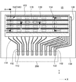
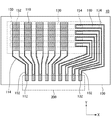
図4は、実施例1に係る発光装置10の平面図である。図5は、図4から隔壁170、第2電極130、有機層120、及び絶縁層150を取り除いた図である。図6は図4のA−A断面図であり、図7は図4のB−B断面図であり、図8は図4のC−C断面図である。
Example 1
FIG. 4 is a plan view of the
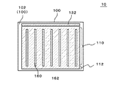
本実施例に係る発光装置10は表示装置であり、基板100、第1電極110、複数の第1端子112、複数の第2端子132、発光部140、絶縁層150、複数の開口152、複数の開口154、複数の引出配線114、有機層120、第2電極130、複数の引出配線134、及び複数の隔壁170を有している。
The
本実施例において、第1電極110の層構造、第1端子112の層構造、及び引出配線114の層構造は、実施形態と同様である。また、第2端子132の層構造は第1端子112の層構造と同様であり、引出配線134の層構造は第2端子132の層構造と同様である。
In this example, the layer structure of the
また、第1電極110は、第1方向(図4におけるY方向)にライン状に延在している。そして第1電極110の端部は、引出配線114に接続している。
The
引出配線114の上には、導体層162が形成されてもよい。導体層162は、引出配線114よりも低抵抗な材料、例えば金属によって形成されている。導体層162は多層構造を有していてもよい。この場合、導体層162は、例えば、Mo又はMo合金などの金属層である第1導電層、Al又はAl合金などの金属層である第2導電層、及び、Mo又はMo合金などの金属層である第3導電層をこの順に積層した構成を有している。第2導電層の厚さは、例えば50nm以上1000nm以下である。好ましくは100nm以下である。また第1導電層及び第3導電層は、第2導電層よりも薄く、例えば30nm以下、好ましくは25nm以下である。なお、導体層162は第1端子112を覆っていない。
A
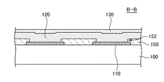
絶縁層150は、例えばポリイミドなどの感光性の樹脂材料によって形成されており、図4、及び図6〜図8に示すように、複数の第1電極110上及びその間の領域に形成されている。絶縁層150には、複数の開口152及び複数の開口154が形成されている。複数の第2電極130は、第1電極110と交差する方向(例えば直交する方向:図4におけるX方向)に互いに平行に延在している。そして、複数の第2電極130の間には、詳細を後述する隔壁170が延在している。開口152は、平面視で第1電極110と第2電極130の交点に位置している。具体的には、複数の開口152は、第1電極110が延在する方向(図4におけるY方向)に並んでいる。また、複数の開口152は、第2電極130の延在方向(図4におけるX方向)にも並んでいる。このため、複数の開口152はマトリクスを構成するように配置されていることになる。
The insulating
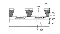
開口154は、平面視で複数の第2電極130のそれぞれの一端側と重なる領域に位置している。また開口154は、開口152が構成するマトリクスの一辺に沿って配置されている。そしてこの一辺に沿う方向(例えば図4におけるY方向、すなわち第1電極110に沿う方向)で見た場合、開口154は、所定の間隔で配置されている。開口154からは、引出配線134の一部分が露出している。そして、引出配線134は、開口154を介して第2電極130に接続している。
The
引出配線134は、第2電極130を第2端子132に接続する配線であり、第1電極110と同一の材料からなる層を有している。引出配線134の一端側は開口154の下に位置しており、引出配線134の他端側は、絶縁層150の外部に引き出されている。そして本図に示す例では、引出配線134の他端側は第2端子132となっている。そして引出配線134の上には、導体層162が形成されてもよい。導体層162は第2端子132を覆っていない。
The
開口152と重なる領域には、有機層120が形成されている。有機層120の正孔輸送層は第1電極110に接しており、有機層120の電子輸送層は第2電極130に接している。このため、発光部140は、開口152と重なる領域それぞれに位置していることになる。
In the region overlapping with the
なお、図6及び図7に示す例では、有機層120を構成する各層は、いずれも開口152の外側まではみ出している場合を示している。そして図4に示すように、有機層120は、隔壁170が延在する方向において、隣り合う開口152の間にも連続して形成されていてもよいし、連続して形成していなくてもよい。ただし、図8に示すように、有機層120は、開口154には形成されていない。
In the example shown in FIG. 6 and FIG. 7, each layer constituting the
第2電極130は、図4、図6〜図8に示すように、第1方向と交わる第2方向(図4におけるX方向)に延在している。そして隣り合う第2電極130の間には、隔壁170が形成されている。隔壁170は、第2電極130と平行すなわち第2方向に延在している。隔壁170の下地は、例えば絶縁層150である。隔壁170は、例えばポリイミド系樹脂などの感光性の樹脂であり、露光及び現像されることによって、所望のパターンに形成されている。なお、隔壁170はポリイミド系樹脂以外の樹脂、例えばエポキシ系樹脂やアクリル系樹脂、二酸化珪素等の無機材料で構成されていても良い。
As shown in FIGS. 4 and 6 to 8, the
隔壁170は、断面が台形の上下を逆にした形状(逆台形)になっている。すなわち隔壁170の上面の幅は、隔壁170の下面の幅よりも大きい。このため、隔壁170を第2電極130より前に形成しておくと、蒸着法やスパッタリング法を用いて、第2電極130を基板100の一面側に形成することで、複数の第2電極130を一括で形成することができる。また、隔壁170は、有機層120を分断する機能も有している。
The
また、第1端子112及び第2端子132には、FPC200が接続している。本図に示す例では、第1端子112及び第2端子132は基板100の同一の辺に沿って配置されている。このため、第1端子112及び第2端子132を、一つのFPC200に接続することができる。
The
次に、本実施例における発光装置10の製造方法を説明する。まず、基板100上に第1電極110、第1端子112、第2端子132、及び引出配線114,134を形成する。これらの形成方法は、実施形態において第1電極110及び第1端子112を形成する方法と同様である。
Next, a method for manufacturing the
次いで、引出配線114上及び引出配線134上を含む領域に、導体層162となる導電膜を形成する。次いで、この導電膜を、例えばフォトリソグラフィー法を利用して所定のパターンにする。これにより、導体層162が形成される。
Next, a conductive film to be the
次いで、第1電極110上に、絶縁層150となる絶縁膜を、例えば塗布法を用いて形成する。次いで、この絶縁膜を露光及び現像する。これにより、絶縁層150が形成される。この工程において、開口152,154も形成される。
Next, an insulating film to be the insulating
次いで、隔壁170を形成する。隔壁170の形成方法も、絶縁層150の形成方法と同様である。さらに有機層120及び第2電極130を形成する。これらの形成方法は、実施形態と同様である。
Next, the
本実施例において、第1端子112及び第2端子132は、実施形態における第1端子112と同様の構成を有している。このため、実施形態と同様に、FPC200を第1端子112及び第2端子132に押し付ける力は第2層112bで吸収される。従って、FPC200を第1端子112に接続する工程において基板100が破損することを抑制できる。また、第2層112bは第1端子112の表層に位置しているため、実施形態と同様に、FPC200を第1端子112に押し付ける力を小さくすることができる。
In the present example, the
(実施例2)
図9は、実施例2に係る発光装置10の構成を示す平面図である。図10は、図9から第2電極130を取り除いた図である。図11は、図10から有機層120を取り除いた図である。本図に示す発光装置10は照明装置である。このため、発光部140は基板100の縁を除いた領域に形成されている。
(Example 2)
FIG. 9 is a plan view illustrating the configuration of the
詳細には、第1電極110は基板100のほぼ全面に形成されている。絶縁層150は第1電極110の縁を覆っている。絶縁層150は、第1電極110の縁において第1電極110と第2電極130が短絡することを防止している。また、有機層120は、第1電極110のうち絶縁層150で囲まれた領域の中に形成されている。言い換えると、絶縁層150は発光部140を画定している。
Specifically, the
第1電極110の上には複数の補助電極160が形成されている。補助電極160は、実施例1における導体層162と同様の層構造を有しており、第1の方向(図9における上下方向)に延在している。補助電極160を設けることにより、第1電極110の見かけ上の抵抗を下げることができる。
A plurality of
本実施例において、第1端子112及び第2端子132の層構造は、実施例1と同様であり、少なくとも第1層112aが第1電極110と一体になっている。第1電極110が第1層112a及び第2層112bの積層構造を有している場合、第1端子112の全体が第1電極110と一体になっている。
In the present embodiment, the layer structure of the
本実施例において、第1端子112及び第2端子132は、実施形態における第1端子112と同様の構成を有している。このため、実施形態と同様に、FPC200を第1端子112及び第2端子132に押し付ける力は第2層112bが柔らかいため小さい力で良い。従って、FPC200を第1端子112に接続する工程において基板100が破損することを抑制できる。
In the present example, the
以上、図面を参照して実施形態及び実施例について述べたが、これらは本発明の例示であり、上記以外の様々な構成を採用することもできる。 As mentioned above, although embodiment and the Example were described with reference to drawings, these are illustrations of this invention and can also employ | adopt various structures other than the above.
10 発光装置
100 基板
110 第1電極
112 第1端子
112a 第1層
112b 第2層
114 引出配線
120 有機層
130 第2電極
132 第2端子
140 発光部
162 導体層
DESCRIPTION OF
Claims (9)
前記基板の上側に形成された端子と、
前記端子と電気的に接続する発光部と、
を備え、
前記端子は、
第1層と、
前記第1層よりも上側に位置し、前記第1層よりも柔らかい第2層と、
を備える発光装置。 A substrate,
Terminals formed on the upper side of the substrate;
A light emitting portion electrically connected to the terminal;
With
The terminal is
The first layer;
A second layer located above the first layer and softer than the first layer;
A light emitting device comprising:
前記第2層は前記端子の表層に位置している発光装置。 The light-emitting device according to claim 1.
The light emitting device, wherein the second layer is located on a surface layer of the terminal.
前記第2層の密度は前記第1層の密度よりも低い発光装置。 The light-emitting device according to claim 1 or 2,
The light emitting device has a density of the second layer lower than a density of the first layer.
前記基板は透光性を有しており、
前記端子は透明導電材料を用いて形成されている発光装置。 In the light-emitting device as described in any one of Claims 1-4,
The substrate has translucency,
The terminal is a light emitting device formed using a transparent conductive material.
前記透明導電材料はITO又はIZOである発光装置。 The light emitting device according to claim 5.
The light emitting device, wherein the transparent conductive material is ITO or IZO.
前記基板は可撓性のある樹脂を有している発光装置。 In the light-emitting device as described in any one of Claims 1-6,
The light emitting device, wherein the substrate includes a flexible resin.
前記基板は厚み200μm以下のガラスを有している発光装置。 In the light-emitting device as described in any one of Claims 1-6,
The light emitting device in which the substrate has glass having a thickness of 200 μm or less.
前記基板に、前記端子に接続する発光部を形成する工程と、
を備え、
前記端子を形成する工程は、
スパッタリングにより第1層を形成する工程と、
前記スパッタリングの入力電力を下げることにより、前記第1層より柔らかい第2層を前記第1層の上に形成する工程と、
を含む発光装置の製造方法。 Forming a terminal on the substrate;
Forming a light emitting portion connected to the terminal on the substrate;
With
The step of forming the terminal includes
Forming a first layer by sputtering;
Forming a second layer softer than the first layer on the first layer by reducing the input power of the sputtering;
A method for manufacturing a light-emitting device including:
Priority Applications (1)
| Application Number | Priority Date | Filing Date | Title |
|---|---|---|---|
| JP2014235863A JP2016100172A (en) | 2014-11-20 | 2014-11-20 | Light-emitting device and method for manufacturing light-emitting device |
Applications Claiming Priority (1)
| Application Number | Priority Date | Filing Date | Title |
|---|---|---|---|
| JP2014235863A JP2016100172A (en) | 2014-11-20 | 2014-11-20 | Light-emitting device and method for manufacturing light-emitting device |
Related Child Applications (1)
| Application Number | Title | Priority Date | Filing Date |
|---|---|---|---|
| JP2020000761A Division JP2020057627A (en) | 2020-01-07 | 2020-01-07 | Light-emitting device |
Publications (1)
| Publication Number | Publication Date |
|---|---|
| JP2016100172A true JP2016100172A (en) | 2016-05-30 |
Family
ID=56077357
Family Applications (1)
| Application Number | Title | Priority Date | Filing Date |
|---|---|---|---|
| JP2014235863A Pending JP2016100172A (en) | 2014-11-20 | 2014-11-20 | Light-emitting device and method for manufacturing light-emitting device |
Country Status (1)
| Country | Link |
|---|---|
| JP (1) | JP2016100172A (en) |
Citations (4)
| Publication number | Priority date | Publication date | Assignee | Title |
|---|---|---|---|---|
| JPS63279597A (en) * | 1987-05-08 | 1988-11-16 | Matsushita Electric Ind Co Ltd | Thin film electroluminescent element and manufacture thereof |
| JPH03112088A (en) * | 1989-09-27 | 1991-05-13 | Hitachi Chem Co Ltd | Thin film el element |
| JP2001056480A (en) * | 1999-08-19 | 2001-02-27 | Seiko Epson Corp | Electro-optic device and its production |
| JP2007010834A (en) * | 2005-06-29 | 2007-01-18 | Sumitomo Chemical Co Ltd | Substrate for display, and display element using it |
-
2014
- 2014-11-20 JP JP2014235863A patent/JP2016100172A/en active Pending
Patent Citations (4)
| Publication number | Priority date | Publication date | Assignee | Title |
|---|---|---|---|---|
| JPS63279597A (en) * | 1987-05-08 | 1988-11-16 | Matsushita Electric Ind Co Ltd | Thin film electroluminescent element and manufacture thereof |
| JPH03112088A (en) * | 1989-09-27 | 1991-05-13 | Hitachi Chem Co Ltd | Thin film el element |
| JP2001056480A (en) * | 1999-08-19 | 2001-02-27 | Seiko Epson Corp | Electro-optic device and its production |
| JP2007010834A (en) * | 2005-06-29 | 2007-01-18 | Sumitomo Chemical Co Ltd | Substrate for display, and display element using it |
Similar Documents
| Publication | Publication Date | Title |
|---|---|---|
| US20240099050A1 (en) | Light-emitting device | |
| JP6595066B2 (en) | Light emitting device manufacturing method and light emitting device | |
| JP7390508B2 (en) | Light-emitting device and method for manufacturing the light-emitting device | |
| JP2016119201A (en) | Light-emitting device | |
| JPWO2016151820A1 (en) | Light emitting device | |
| JP2016100172A (en) | Light-emitting device and method for manufacturing light-emitting device | |
| JP6555911B2 (en) | Light emitting device | |
| JP6441306B2 (en) | Light emitting device | |
| WO2017163331A1 (en) | Light emitting device, electronic device, and manufacturing method for light emitting device | |
| JP2016095990A (en) | Light emission device | |
| JP2016157645A (en) | Light emission device | |
| JP2016186911A (en) | Light emission device | |
| JP6580336B2 (en) | Light emitting device | |
| JP6499876B2 (en) | Light emitting device | |
| JP6496138B2 (en) | Light emitting device | |
| JP2020013797A (en) | Light-emitting device manufacturing method | |
| JP2022164806A (en) | Light-emitting device | |
| WO2016129114A1 (en) | Light-emitting device and method for producing light-emitting device | |
| JP2019201004A (en) | Light-emitting device | |
| JP2019165026A (en) | Light-emitting device | |
| JP2016178061A (en) | Light emitting device manufacturing method | |
| JP2016095991A (en) | Light emission device | |
| JP2016143529A (en) | Light emission device | |
| JP2016184545A (en) | Light emission device and light emission system | |
| JP2016149315A (en) | Manufacturing method for light-emitting device |
Legal Events
| Date | Code | Title | Description |
|---|---|---|---|
| A621 | Written request for application examination |
Free format text: JAPANESE INTERMEDIATE CODE: A621 Effective date: 20171005 |
|
| A977 | Report on retrieval |
Free format text: JAPANESE INTERMEDIATE CODE: A971007 Effective date: 20180820 |
|
| A131 | Notification of reasons for refusal |
Free format text: JAPANESE INTERMEDIATE CODE: A131 Effective date: 20180918 |
|
| A521 | Request for written amendment filed |
Free format text: JAPANESE INTERMEDIATE CODE: A523 Effective date: 20181114 |
|
| A131 | Notification of reasons for refusal |
Free format text: JAPANESE INTERMEDIATE CODE: A131 Effective date: 20190312 |
|
| A02 | Decision of refusal |
Free format text: JAPANESE INTERMEDIATE CODE: A02 Effective date: 20191008 |