JP2016099114A - Electronic device, physical quantity sensor, pressure sensor, altimeter, electronic apparatus and moving body - Google Patents
Electronic device, physical quantity sensor, pressure sensor, altimeter, electronic apparatus and moving body Download PDFInfo
- Publication number
- JP2016099114A JP2016099114A JP2014233352A JP2014233352A JP2016099114A JP 2016099114 A JP2016099114 A JP 2016099114A JP 2014233352 A JP2014233352 A JP 2014233352A JP 2014233352 A JP2014233352 A JP 2014233352A JP 2016099114 A JP2016099114 A JP 2016099114A
- Authority
- JP
- Japan
- Prior art keywords
- layer
- electronic device
- substrate
- corrosion
- physical quantity
- Prior art date
- Legal status (The legal status is an assumption and is not a legal conclusion. Google has not performed a legal analysis and makes no representation as to the accuracy of the status listed.)
- Withdrawn
Links
Images


Classifications
-
- B—PERFORMING OPERATIONS; TRANSPORTING
- B81—MICROSTRUCTURAL TECHNOLOGY
- B81B—MICROSTRUCTURAL DEVICES OR SYSTEMS, e.g. MICROMECHANICAL DEVICES
- B81B3/00—Devices comprising flexible or deformable elements, e.g. comprising elastic tongues or membranes
- B81B3/0018—Structures acting upon the moving or flexible element for transforming energy into mechanical movement or vice versa, i.e. actuators, sensors, generators
- B81B3/0021—Transducers for transforming electrical into mechanical energy or vice versa
-
- B—PERFORMING OPERATIONS; TRANSPORTING
- B81—MICROSTRUCTURAL TECHNOLOGY
- B81C—PROCESSES OR APPARATUS SPECIALLY ADAPTED FOR THE MANUFACTURE OR TREATMENT OF MICROSTRUCTURAL DEVICES OR SYSTEMS
- B81C1/00—Manufacture or treatment of devices or systems in or on a substrate
- B81C1/00777—Preserve existing structures from alteration, e.g. temporary protection during manufacturing
- B81C1/00785—Avoid chemical alteration, e.g. contamination, oxidation or unwanted etching
- B81C1/00801—Avoid alteration of functional structures by etching, e.g. using a passivation layer or an etch stop layer
-
- B—PERFORMING OPERATIONS; TRANSPORTING
- B81—MICROSTRUCTURAL TECHNOLOGY
- B81C—PROCESSES OR APPARATUS SPECIALLY ADAPTED FOR THE MANUFACTURE OR TREATMENT OF MICROSTRUCTURAL DEVICES OR SYSTEMS
- B81C1/00—Manufacture or treatment of devices or systems in or on a substrate
- B81C1/00015—Manufacture or treatment of devices or systems in or on a substrate for manufacturing microsystems
- B81C1/00261—Processes for packaging MEMS devices
- B81C1/00277—Processes for packaging MEMS devices for maintaining a controlled atmosphere inside of the cavity containing the MEMS
- B81C1/00293—Processes for packaging MEMS devices for maintaining a controlled atmosphere inside of the cavity containing the MEMS maintaining a controlled atmosphere with processes not provided for in B81C1/00285
-
- G—PHYSICS
- G01—MEASURING; TESTING
- G01L—MEASURING FORCE, STRESS, TORQUE, WORK, MECHANICAL POWER, MECHANICAL EFFICIENCY, OR FLUID PRESSURE
- G01L1/00—Measuring force or stress, in general
- G01L1/18—Measuring force or stress, in general using properties of piezo-resistive materials, i.e. materials of which the ohmic resistance varies according to changes in magnitude or direction of force applied to the material
-
- G—PHYSICS
- G01—MEASURING; TESTING
- G01L—MEASURING FORCE, STRESS, TORQUE, WORK, MECHANICAL POWER, MECHANICAL EFFICIENCY, OR FLUID PRESSURE
- G01L5/00—Apparatus for, or methods of, measuring force, work, mechanical power, or torque, specially adapted for specific purposes
- G01L5/04—Apparatus for, or methods of, measuring force, work, mechanical power, or torque, specially adapted for specific purposes for measuring tension in flexible members, e.g. ropes, cables, wires, threads, belts or bands
- G01L5/06—Apparatus for, or methods of, measuring force, work, mechanical power, or torque, specially adapted for specific purposes for measuring tension in flexible members, e.g. ropes, cables, wires, threads, belts or bands using mechanical means
-
- G—PHYSICS
- G01—MEASURING; TESTING
- G01L—MEASURING FORCE, STRESS, TORQUE, WORK, MECHANICAL POWER, MECHANICAL EFFICIENCY, OR FLUID PRESSURE
- G01L9/00—Measuring steady of quasi-steady pressure of fluid or fluent solid material by electric or magnetic pressure-sensitive elements; Transmitting or indicating the displacement of mechanical pressure-sensitive elements, used to measure the steady or quasi-steady pressure of a fluid or fluent solid material, by electric or magnetic means
- G01L9/0041—Transmitting or indicating the displacement of flexible diaphragms
- G01L9/0042—Constructional details associated with semiconductive diaphragm sensors, e.g. etching, or constructional details of non-semiconductive diaphragms
- G01L9/0045—Diaphragm associated with a buried cavity
-
- G—PHYSICS
- G01—MEASURING; TESTING
- G01L—MEASURING FORCE, STRESS, TORQUE, WORK, MECHANICAL POWER, MECHANICAL EFFICIENCY, OR FLUID PRESSURE
- G01L9/00—Measuring steady of quasi-steady pressure of fluid or fluent solid material by electric or magnetic pressure-sensitive elements; Transmitting or indicating the displacement of mechanical pressure-sensitive elements, used to measure the steady or quasi-steady pressure of a fluid or fluent solid material, by electric or magnetic means
- G01L9/0041—Transmitting or indicating the displacement of flexible diaphragms
- G01L9/0051—Transmitting or indicating the displacement of flexible diaphragms using variations in ohmic resistance
- G01L9/0052—Transmitting or indicating the displacement of flexible diaphragms using variations in ohmic resistance of piezoresistive elements
- G01L9/0054—Transmitting or indicating the displacement of flexible diaphragms using variations in ohmic resistance of piezoresistive elements integral with a semiconducting diaphragm
-
- G—PHYSICS
- G01—MEASURING; TESTING
- G01L—MEASURING FORCE, STRESS, TORQUE, WORK, MECHANICAL POWER, MECHANICAL EFFICIENCY, OR FLUID PRESSURE
- G01L9/00—Measuring steady of quasi-steady pressure of fluid or fluent solid material by electric or magnetic pressure-sensitive elements; Transmitting or indicating the displacement of mechanical pressure-sensitive elements, used to measure the steady or quasi-steady pressure of a fluid or fluent solid material, by electric or magnetic means
- G01L9/0041—Transmitting or indicating the displacement of flexible diaphragms
- G01L9/0072—Transmitting or indicating the displacement of flexible diaphragms using variations in capacitance
- G01L9/0073—Transmitting or indicating the displacement of flexible diaphragms using variations in capacitance using a semiconductive diaphragm
-
- G—PHYSICS
- G01—MEASURING; TESTING
- G01L—MEASURING FORCE, STRESS, TORQUE, WORK, MECHANICAL POWER, MECHANICAL EFFICIENCY, OR FLUID PRESSURE
- G01L9/00—Measuring steady of quasi-steady pressure of fluid or fluent solid material by electric or magnetic pressure-sensitive elements; Transmitting or indicating the displacement of mechanical pressure-sensitive elements, used to measure the steady or quasi-steady pressure of a fluid or fluent solid material, by electric or magnetic means
- G01L9/0041—Transmitting or indicating the displacement of flexible diaphragms
- G01L9/008—Transmitting or indicating the displacement of flexible diaphragms using piezoelectric devices
-
- H—ELECTRICITY
- H01—ELECTRIC ELEMENTS
- H01L—SEMICONDUCTOR DEVICES NOT COVERED BY CLASS H10
- H01L21/00—Processes or apparatus adapted for the manufacture or treatment of semiconductor or solid state devices or of parts thereof
- H01L21/70—Manufacture or treatment of devices consisting of a plurality of solid state components formed in or on a common substrate or of parts thereof; Manufacture of integrated circuit devices or of parts thereof
- H01L21/71—Manufacture of specific parts of devices defined in group H01L21/70
- H01L21/76—Making of isolation regions between components
- H01L21/762—Dielectric regions, e.g. EPIC dielectric isolation, LOCOS; Trench refilling techniques, SOI technology, use of channel stoppers
- H01L21/7624—Dielectric regions, e.g. EPIC dielectric isolation, LOCOS; Trench refilling techniques, SOI technology, use of channel stoppers using semiconductor on insulator [SOI] technology
- H01L21/76264—SOI together with lateral isolation, e.g. using local oxidation of silicon, or dielectric or polycristalline material refilled trench or air gap isolation regions, e.g. completely isolated semiconductor islands
- H01L21/76283—Lateral isolation by refilling of trenches with dielectric material
-
- B—PERFORMING OPERATIONS; TRANSPORTING
- B81—MICROSTRUCTURAL TECHNOLOGY
- B81C—PROCESSES OR APPARATUS SPECIALLY ADAPTED FOR THE MANUFACTURE OR TREATMENT OF MICROSTRUCTURAL DEVICES OR SYSTEMS
- B81C1/00—Manufacture or treatment of devices or systems in or on a substrate
- B81C1/00015—Manufacture or treatment of devices or systems in or on a substrate for manufacturing microsystems
- B81C1/00134—Manufacture or treatment of devices or systems in or on a substrate for manufacturing microsystems comprising flexible or deformable structures
- B81C1/00158—Diaphragms, membranes
-
- B—PERFORMING OPERATIONS; TRANSPORTING
- B81—MICROSTRUCTURAL TECHNOLOGY
- B81C—PROCESSES OR APPARATUS SPECIALLY ADAPTED FOR THE MANUFACTURE OR TREATMENT OF MICROSTRUCTURAL DEVICES OR SYSTEMS
- B81C2201/00—Manufacture or treatment of microstructural devices or systems
- B81C2201/01—Manufacture or treatment of microstructural devices or systems in or on a substrate
- B81C2201/0101—Shaping material; Structuring the bulk substrate or layers on the substrate; Film patterning
- B81C2201/0128—Processes for removing material
- B81C2201/013—Etching
- B81C2201/0135—Controlling etch progression
- B81C2201/014—Controlling etch progression by depositing an etch stop layer, e.g. silicon nitride, silicon oxide, metal
-
- B—PERFORMING OPERATIONS; TRANSPORTING
- B81—MICROSTRUCTURAL TECHNOLOGY
- B81C—PROCESSES OR APPARATUS SPECIALLY ADAPTED FOR THE MANUFACTURE OR TREATMENT OF MICROSTRUCTURAL DEVICES OR SYSTEMS
- B81C2203/00—Forming microstructural systems
- B81C2203/01—Packaging MEMS
- B81C2203/0136—Growing or depositing of a covering layer
Abstract
Description
本発明は、電子デバイス、物理量センサー、圧力センサー、高度計、電子機器および移
動体に関するものである。
The present invention relates to an electronic device, a physical quantity sensor, a pressure sensor, an altimeter, an electronic apparatus, and a moving object.
半導体製造プロセスを用いて形成された空洞部を有する電子デバイスが知られている(
例えば、特許文献1参照)。このような電子デバイスの一例としては、例えば、特許文献
1に係る電子装置が挙げられ、この電子装置は、基板と、基板に設けられたMEMS構造
体と、被覆構造体と、を含み、被覆構造体が、包囲壁と、第1被覆層と、第2被覆層と、
を有し、包囲壁、第1被覆層、第2被覆層および基板によって、MEMS構造体が配置さ
れた空洞部が画成されている。
Electronic devices having cavities formed using a semiconductor manufacturing process are known (
For example, see Patent Document 1). As an example of such an electronic device, for example, an electronic apparatus according to
A cavity in which the MEMS structure is disposed is defined by the surrounding wall, the first covering layer, the second covering layer, and the substrate.
しかし、特許文献1に係る電子装置では、ウェットエッチングを用いて空洞部を形成す
る際に、レジストで構成されたマスクとの隙間からエッチング液が侵入し、それによって
不本意なエッチングが生じ、その結果、空洞部の気密性が低下するという問題があった。
However, in the electronic device according to
本発明の目的は、優れた信頼性を有する電子デバイスおよび物理量センサーを提供する
こと、また、かかる電子デバイスを備える圧力センサー、高度計、電子機器および移動体
を提供することにある。
An object of the present invention is to provide an electronic device and a physical quantity sensor having excellent reliability, and to provide a pressure sensor, an altimeter, an electronic apparatus, and a moving body including the electronic device.
このような目的は、下記の本発明により達成される。
[適用例1]
本発明の電子デバイスは、基板と、
前記基板の一方の面側に配置されている機能素子と、
前記基板の前記一方の面側に前記基板の平面視で前記機能素子を囲んで配置されている
壁部と、
前記壁部に対して前記基板とは反対側に配置されていて、前記壁部とともに内部空間を
構成している天井部と、
を備え、
前記壁部は、絶縁層と、前記絶縁層をエッチング可能なエッチング液に対する耐性が前
記絶縁層よりも高い複数の耐蝕層と、を有し、
前記基板と交差する方向の断面視で、前記複数の耐蝕層が接続して前記絶縁層の周囲に
配置されていることを特徴とする。
Such an object is achieved by the present invention described below.
[Application Example 1]
An electronic device of the present invention includes a substrate,
A functional element disposed on one side of the substrate;
A wall portion disposed around the functional element in a plan view of the substrate on the one surface side of the substrate;
A ceiling part which is disposed on the opposite side of the substrate with respect to the wall part and constitutes an internal space together with the wall part;
With
The wall portion includes an insulating layer, and a plurality of corrosion-resistant layers having higher resistance to an etchant capable of etching the insulating layer than the insulating layer,
The plurality of corrosion-resistant layers are connected and arranged around the insulating layer in a cross-sectional view in a direction crossing the substrate.
このような電子デバイスによれば、複数の耐蝕層が互いに接続して絶縁層を囲んでいる
ことにより、内部空間を形成する際に用いるエッチング液により壁部(特に絶縁層)がエ
ッチングされてしまうのを低減することができる。よって、優れた信頼性を有する電子デ
バイスを提供することができる。
According to such an electronic device, a plurality of corrosion-resistant layers are connected to each other and surround the insulating layer, so that the wall (particularly the insulating layer) is etched by the etching solution used when forming the internal space. Can be reduced. Therefore, an electronic device having excellent reliability can be provided.
[適用例2]
本発明の電子デバイスでは、前記複数の耐蝕層は、前記断面視で、第1耐蝕層と、前記
第1耐蝕層に対して2箇所で接続していて前記第1耐蝕層とともに前記絶縁層を囲んでい
る第2耐蝕層と、を有することが好ましい。
これにより、第1耐蝕層および第2耐蝕層の2層により絶縁層を囲むことができる。
[Application Example 2]
In the electronic device according to the aspect of the invention, the plurality of corrosion-resistant layers are connected to the first corrosion-resistant layer and the first corrosion-resistant layer at two locations in the cross-sectional view, and the insulating layer is connected to the first corrosion-resistant layer. It is preferable to have the surrounding 2nd corrosion-resistant layer.
Thereby, the insulating layer can be surrounded by two layers of the first corrosion-resistant layer and the second corrosion-resistant layer.
[適用例3]
本発明の電子デバイスでは、前記第1耐蝕層は、
前記基板に固定されている固定部と、
前記固定部から前記内部空間側に延びていて前記基板と離間している第1フランジ部と
、
前記固定部から前記内部空間とは反対側に延びていて前記基板と離間している第2フラ
ンジ部と、
を有し、
前記第2耐蝕層は、
前記第1フランジ部に接続している第1接続部と、
前記第2フランジ部に接続している第2接続部と、
を有することが好ましい。
[Application Example 3]
In the electronic device of the present invention, the first corrosion-resistant layer is
A fixing portion fixed to the substrate;
A first flange portion extending from the fixed portion toward the internal space and spaced apart from the substrate;
A second flange portion extending from the fixed portion to the opposite side of the internal space and spaced from the substrate;
Have
The second corrosion resistant layer is
A first connecting portion connected to the first flange portion;
A second connecting portion connected to the second flange portion;
It is preferable to have.
これにより、壁部の基板とは反対側の段差を低減することができる。そのため、壁部お
よび天井部を構成する各層の密着性を高めて、内部空間の気密性の低下を効果的に低減す
ることができる。また、内部空間をエッチングにより形成する際に用いるマスクの密着性
を高めることができ、その結果、不本意なエッチングを低減することができる。
Thereby, the level | step difference on the opposite side to the board | substrate of a wall part can be reduced. Therefore, the adhesiveness of each layer which comprises a wall part and a ceiling part can be improved, and the fall of the airtightness of internal space can be reduced effectively. In addition, the adhesion of the mask used when the internal space is formed by etching can be increased, and as a result, unintentional etching can be reduced.
[適用例4]
本発明の電子デバイスでは、前記耐蝕層は、金属を含んでいることが好ましい。
金属は、高精度な成膜が可能であるとともに、シリコン酸化膜で構成された絶縁層のエ
ッチングに用いるエッチングに対して高い耐性を有する。したがって、耐蝕層が金属を含
んでいることにより、高精度な壁部を形成することができる。
[Application Example 4]
In the electronic device of the present invention, it is preferable that the corrosion-resistant layer contains a metal.
A metal can be formed with high accuracy and has high resistance to etching used for etching an insulating layer formed of a silicon oxide film. Therefore, a highly accurate wall part can be formed because the corrosion-resistant layer contains a metal.
[適用例5]
本発明の電子デバイスでは、前記金属は、アルミニウムを含んでいることが好ましい。
アルミニウムは、金属の中でも、半導体製造プロセスとの親和性が高い。したがって、
耐蝕層がアルミニウムを含んでいることにより、比較的簡単に、高精度な壁部を形成する
ことができる。
[Application Example 5]
In the electronic device according to the aspect of the invention, it is preferable that the metal contains aluminum.
Aluminum is highly compatible with semiconductor manufacturing processes among metals. Therefore,
Since the corrosion-resistant layer contains aluminum, a highly accurate wall can be formed relatively easily.
[適用例6]
本発明の電子デバイスでは、前記絶縁層は、酸化シリコンを含んでいることが好ましい
。
[Application Example 6]
In the electronic device of the present invention, it is preferable that the insulating layer contains silicon oxide.
酸化シリコン(SiO2)は、絶縁性を有し、犠牲層の材料として適している。そのた
め、比較的簡単に、高精度な壁部および内部空間を形成することができる。
Silicon oxide (SiO 2 ) has an insulating property and is suitable as a material for the sacrificial layer. Therefore, a highly accurate wall part and internal space can be formed relatively easily.
[適用例7]
本発明の電子デバイスでは、前記基板は、平面視で前記天井部と重なる位置に設けられ
ていて、受圧により撓み変形するダイヤフラム部を有することが好ましい。
[Application Example 7]
In the electronic device according to the aspect of the invention, it is preferable that the substrate has a diaphragm portion that is provided at a position overlapping the ceiling portion in a plan view and bends and deforms by receiving pressure.
これにより、圧力を検出可能な電子デバイス(物理量センサー)を実現することができ
る。
Thereby, an electronic device (physical quantity sensor) capable of detecting pressure can be realized.
[適用例8]
本発明の電子デバイスでは、前記機能素子は、歪みにより電気信号を出力するセンサー
素子であることが好ましい。
これにより、圧力の検出感度を向上させることができる。
[Application Example 8]
In the electronic device according to the aspect of the invention, it is preferable that the functional element is a sensor element that outputs an electric signal by strain.
Thereby, the pressure detection sensitivity can be improved.
[適用例9]
本発明の物理量センサーは、前記機能素子が前記ダイヤフラム部の一方の面側に配置さ
れているセンサー素子である本発明の電子デバイス、を備えることを特徴とする。
これにより、優れた信頼性を有する物理量センサーを提供することができる。
[Application Example 9]
The physical quantity sensor of the present invention includes the electronic device of the present invention, which is a sensor element in which the functional element is disposed on one surface side of the diaphragm portion.
Thereby, it is possible to provide a physical quantity sensor having excellent reliability.
[適用例10]
本発明の圧力センサーは、本発明の電子デバイスを備えることを特徴とする。
これにより、優れた信頼性を有する圧力センサーを提供することができる。
[Application Example 10]
The pressure sensor of the present invention includes the electronic device of the present invention.
Thereby, the pressure sensor which has the outstanding reliability can be provided.
[適用例11]
本発明の高度計は、本発明の電子デバイスを備えることを特徴とする。
これにより、優れた信頼性を有する高度計を提供することができる。
[Application Example 11]
An altimeter according to the present invention includes the electronic device according to the present invention.
Thereby, the altimeter which has the outstanding reliability can be provided.
[適用例12]
本発明の電子機器は、本発明の電子デバイスを備えることを特徴とする。
これにより、優れた信頼性を有する電子機器を提供することができる。
[Application Example 12]
An electronic apparatus according to the present invention includes the electronic device according to the present invention.
Thereby, an electronic device having excellent reliability can be provided.
[適用例13]
本発明の移動体は、本発明の電子デバイスを備えることを特徴とする。
これにより、優れた信頼性を有する移動体を提供することができる。
[Application Example 13]
The moving body of the present invention includes the electronic device of the present invention.
Thereby, the mobile body which has the outstanding reliability can be provided.
以下、本発明の電子デバイス、物理量センサー、圧力センサー、高度計、電子機器およ
び移動体を添付図面に示す各実施形態に基づいて詳細に説明する。
Hereinafter, an electronic device, a physical quantity sensor, a pressure sensor, an altimeter, an electronic device, and a moving body of the present invention will be described in detail based on each embodiment shown in the accompanying drawings.
1.物理量センサー
図1は、本発明の実施形態に係る物理量センサーを示す断面図、図2は、図1に示す物
理量センサーのピエゾ抵抗素子(センサー素子)の配置を示す平面図である。図3は、図
1に示す物理量センサーの作用を説明するための図であって、図3(a)は加圧状態を示
す断面図、図3(b)は加圧状態を示す平面図である。なお、以下では、説明の便宜上、
図1中の上側を「上」、下側を「下」という。
1. Physical Quantity Sensor FIG. 1 is a cross-sectional view showing a physical quantity sensor according to an embodiment of the present invention, and FIG. 2 is a plan view showing an arrangement of piezoresistive elements (sensor elements) of the physical quantity sensor shown in FIG. 3A and 3B are diagrams for explaining the operation of the physical quantity sensor shown in FIG. 1, in which FIG. 3A is a cross-sectional view showing a pressurized state, and FIG. 3B is a plan view showing the pressurized state. is there. In the following, for convenience of explanation,
The upper side in FIG. 1 is referred to as “upper” and the lower side is referred to as “lower”.
図1に示す物理量センサー1は、ダイヤフラム部20を有する基板2と、ダイヤフラム
部20に配置されている機能素子である複数のピエゾ抵抗素子5(センサー素子)と、基
板2とともに空洞部S(内部空間)を形成している積層構造体6と、基板2と積層構造体
6との間に配置されている中間層3と、を備えている。
A
以下、物理量センサー1を構成する各部を順次説明する。
−基板−
基板2は、半導体基板21と、半導体基板21の一方の面上に設けられた絶縁膜22と
、絶縁膜22の半導体基板21とは反対側の面上に設けられた絶縁膜23と、を有してい
る。
Hereinafter, each part which comprises the
-Board-
The
半導体基板21は、単結晶シリコンで構成されているシリコン層211(ハンドル層)
と、シリコン酸化膜で構成されている酸化シリコン層212(ボックス層)と、単結晶シ
リコンで構成されているシリコン層213(デバイス層)とがこの順で積層されたSOI
基板である。なお、半導体基板21は、SOI基板に限定されず、例えば、単結晶シリコ
ン基板等の他の半導体基板であってもよい。
The
And an SOI in which a silicon oxide layer 212 (box layer) made of a silicon oxide film and a silicon layer 213 (device layer) made of single crystal silicon are stacked in this order.
It is a substrate. The
絶縁膜22は、例えば、シリコン酸化膜であり、絶縁性を有する。また、絶縁膜23は
、例えば、シリコン窒化膜であり、絶縁性を有するとともに、フッ酸を含むエッチング液
に対する耐性をも有する。ここで、半導体基板21(シリコン層213)と絶縁膜23(
シリコン窒化膜)との間に絶縁膜22(シリコン酸化膜)が介在していることにより、絶
縁膜23の成膜時に生じた応力が半導体基板21に伝わるのを絶縁膜22により緩和する
ことができる。また、絶縁膜22は、半導体基板21およびその上方に半導体回路を形成
する場合、素子間分離膜として用いることもできる。なお、絶縁膜22、23は、前述し
た構成材料に限定されず、また、必要に応じて、絶縁膜22、23のうちのいずれか一方
を省略してもよい。
The insulating
Since the insulating film 22 (silicon oxide film) is interposed between the insulating
このような基板2の絶縁膜23上には、パターニングされた中間層3が配置されている
。この中間層3は、平面視でダイヤフラム部20の周囲を囲むように形成されており、中
間層3の上面と基板2の上面との間であって、ダイヤフラム部20の中心側(内側)に中
間層3の厚さ分の段差部を形成する。これにより、ダイヤフラム部20が受圧により撓み
変形したとき、ダイヤフラム部20の段差部との間の境界部分に応力を集中させることが
できる。そのため、かかる境界部分(またはその付近)にピエゾ抵抗素子5を配置するこ
とにより、検出感度を向上させることができる。
A patterned
この中間層3は、例えば、単結晶シリコン、多結晶シリコン(ポリシリコン)またはア
モルファスシリコンで構成されている。また、中間層3は、例えば、単結晶シリコン、多
結晶シリコン(ポリシリコン)またはアモルファスシリコンにリン、ボロン等の不純物を
ドープ(拡散または注入)して構成されていてもよい。この場合、中間層3は、導電性を
有するため、例えば、空洞部Sの外側において基板2上にMOSトランジスタを形成する
場合、中間層3の一部をMOSトランジスタのゲート電極として用いることができる。ま
た、中間層3の一部を配線として用いることもできる。
The
このような基板2には、周囲の部分よりも薄肉であり、受圧によって撓み変形するダイ
ヤフラム部20が設けられている。ダイヤフラム部20は、半導体基板21の下面に有底
の凹部24を設けることで形成されている。すなわち、ダイヤフラム部20は、基板2の
一方の面に開口している凹部24の底部を含んで構成されている。このダイヤフラム部2
0は、その下面が受圧面25となっている。本実施形態では、図2に示すように、ダイヤ
フラム部20は、正方形(矩形)の平面視形状である。
Such a
0 has a
本実施形態の基板2では、凹部24がシリコン層211を貫通しており、ダイヤフラム
部20が酸化シリコン層212、シリコン層213、絶縁膜22および絶縁膜23の4層
で構成されている。ここで、酸化シリコン層212は、後述するように、物理量センサー
1の製造工程において凹部24をエッチングにより形成する際にエッチングストップ層と
して利用することができ、ダイヤフラム部20の厚さの製品ごとのバラツキを少なくする
ことができる。
In the
なお、凹部24がシリコン層211を貫通せず、ダイヤフラム部20がシリコン層21
1の薄肉部、酸化シリコン層212、シリコン層213、絶縁膜22および絶縁膜23の
5層で構成されていてもよい。
Note that the
1 thin-walled portion,
−ピエゾ抵抗素子(機能素子)−
複数のピエゾ抵抗素子5は、図1に示すように、それぞれ、ダイヤフラム部20の空洞
部S側に形成されている。ここで、ピエゾ抵抗素子5は、半導体基板21のシリコン層2
13に形成されている。
-Piezoresistive element (functional element)-
As shown in FIG. 1, the plurality of
13 is formed.
図2に示すように、複数のピエゾ抵抗素子5は、ダイヤフラム部20の外周部に配置さ
れている複数のピエゾ抵抗素子5a、5b、5c、5dで構成されている。
As shown in FIG. 2, the plurality of
基板2の厚さ方向から見た平面視(以下、単に「平面視」という)で四角形をなすダイ
ヤフラム部20の4つの辺にそれぞれ対応して、ピエゾ抵抗素子5a、ピエゾ抵抗素子5
b、ピエゾ抵抗素子5c、ピエゾ抵抗素子5dが配置されている。
The
b, a
ピエゾ抵抗素子5aは、ダイヤフラム部20の対応する辺に対して垂直な方向に沿って
延びている。そして、ピエゾ抵抗素子5aの両端部には、1対の配線214aが電気的に
接続されている。同様に、ピエゾ抵抗素子5bは、ダイヤフラム部20の対応する辺に対
して垂直な方向に沿って延びている。そして、ピエゾ抵抗素子5bの両端部には、1対の
配線214bが電気的に接続されている。
The
一方、ピエゾ抵抗素子5cは、ダイヤフラム部20の対応する辺に対して平行な方向に
沿って延びている。そして、ピエゾ抵抗素子5cの両端部には、1対の配線214cが電
気的に接続されている。同様に、ピエゾ抵抗素子5dは、ダイヤフラム部20の対応する
辺に対して平行な方向に沿って延びている。そして、ピエゾ抵抗素子5dの両端部には、
1対の配線214dが電気的に接続されている。
On the other hand, the
A pair of
なお、以下では、配線214a、214b、214c、214dをまとめて「配線21
4」ともいう。
Hereinafter, the wirings 214a, 214b, 214c, and 214d are collectively referred to as “
4 ".
このようなピエゾ抵抗素子5および配線214は、それぞれ、例えば、リン、ボロン等
の不純物をドープ(拡散または注入)したシリコン(単結晶シリコン)で構成されている
。ここで、配線214における不純物のドープ濃度は、ピエゾ抵抗素子5における不純物
のドープ濃度よりも高い。なお、配線214は、金属で構成されていてもよい。
The
また、複数のピエゾ抵抗素子5は、例えば、自然状態における抵抗値が互いに等しくな
るように構成されている。
Further, the plurality of
以上説明したようなピエゾ抵抗素子5は、配線214等を介して、ブリッジ回路(ホイ
ートストンブリッジ回路)を構成している。このブリッジ回路には、駆動電圧を供給する
駆動回路(図示せず)が接続されている。そして、このブリッジ回路では、ピエゾ抵抗素
子5の抵抗値に応じた信号(電圧)として出力される。
The
−積層構造体−
積層構造体6は、前述した基板2との間に空洞部Sを画成するように形成されている。
ここで、積層構造体6は、ダイヤフラム部20のピエゾ抵抗素子5側に配置されていてダ
イヤフラム部20(または基板2)とともに空洞部S(内部空間)を区画形成(構成)し
ている。
-Laminated structure-
The laminated structure 6 is formed so as to define a cavity S between itself and the
Here, the laminated structure 6 is disposed on the
この積層構造体6は、基板2上に平面視でピエゾ抵抗素子5を取り囲むように形成され
た層間絶縁膜61と、層間絶縁膜61上に形成された配線層62と、配線層62および層
間絶縁膜61上に形成された層間絶縁膜63と、層間絶縁膜63上に形成され、複数の細
孔642(開孔)を備えた被覆層641を有する配線層64と、配線層64および層間絶
縁膜63上に形成された表面保護膜65と、被覆層641上に設けられた封止層66とを
有している。
The laminated structure 6 includes an
層間絶縁膜61、63は、それぞれ、例えば、シリコン酸化膜で構成されている。また
、配線層62、64および封止層66は、それぞれ、アルミニウム等の金属で構成されて
いる。また、封止層66は、被覆層641が有する複数の細孔642を封止している。ま
た、表面保護膜65は、シリコン酸化膜であるSiO2層651と、シリコン窒化膜であ
るSiN層652とがこの順で積層されて構成されている。ここで、主としてSiN層6
52が表面保護の機能を有し、SiO2層651は、SiN層652との間の密着性や平
坦性を高める機能を有する。
The
52 has a function of protecting the surface, and the SiO 2 layer 651 has a function of improving adhesion and flatness with the
このような積層構造体6において、被覆層641を除く配線層62および配線層64か
らなる構造体は、層間絶縁膜63の一部である絶縁層631とともに、基板2の一方の面
側に平面視でピエゾ抵抗素子5を囲んで配置されている「壁部」(ガードリング)を構成
している。また、被覆層641は、この壁部に対して基板2とは反対側に配置されていて
空洞部S(内部空間)を壁部とともに構成している「天井部」を構成している。なお、壁
部およびこれに関連する事項については、後に詳述する。
In such a laminated structure 6, the structure including the
また、このような積層構造体6は、CMOSプロセスのような半導体製造プロセスを用
いて形成することができる。なお、シリコン層213上およびその上方には、半導体回路
が作り込まれていてもよい。この半導体回路は、MOSトランジスタ等の能動素子、その
他必要に応じて形成されたコンデンサ、インダクタ、抵抗、ダイオード、配線(ピエゾ抵
抗素子5に接続されている配線を含む)等の回路要素を有している。
Moreover, such a laminated structure 6 can be formed using a semiconductor manufacturing process such as a CMOS process. Note that a semiconductor circuit may be formed on and above the
基板2と積層構造体6とによって画成された空洞部Sは、密閉された空間である。この
空洞部Sは、物理量センサー1が検出する圧力の基準値となる圧力基準室として機能する
。本実施形態では、空洞部Sが真空状態(300Pa以下)となっている。空洞部Sを真
空状態とすることによって、物理量センサー1を、真空状態を基準として圧力を検出する
「絶対圧センサー」として用いることができ、その利便性が向上する。
The cavity S defined by the
ただし、空洞部Sは、真空状態でなくてもよく、大気圧であってもよいし、大気圧より
も気圧が低い減圧状態であってもよいし、大気圧よりも気圧が高い加圧状態であってもよ
い。また、空洞部Sには、窒素ガス、希ガス等の不活性ガスが封入されていてもよい。
以上、物理量センサー1の構成について簡単に説明した。
However, the cavity S may not be in a vacuum state, may be atmospheric pressure, may be in a reduced pressure state where the atmospheric pressure is lower than atmospheric pressure, or is a pressurized state where the atmospheric pressure is higher than atmospheric pressure. It may be. The cavity S may be filled with an inert gas such as nitrogen gas or a rare gas.
The configuration of the
このような構成の物理量センサー1は、図3(a)に示すように、ダイヤフラム部20
の受圧面25が受ける圧力Pに応じて、ダイヤフラム部20が変形し、これにより、図3
(b)に示すように、ピエゾ抵抗素子5a、5b、5c、5dが歪み、ピエゾ抵抗素子5
a、5b、5c、5dの抵抗値が変化する。それに伴って、ピエゾ抵抗素子5a、5b、
5c、5dが構成するブリッジ回路の出力が変化し、その出力に基づいて、受圧面25で
受けた圧力の大きさを求めることができる。
As shown in FIG. 3A, the
The
As shown in (b), the
The resistance values of a, 5b, 5c, and 5d change. Accordingly,
The output of the bridge circuit formed by 5c and 5d changes, and the magnitude of the pressure received by the
より具体的に説明すると、前述したようなダイヤフラム部20の変形が生じる前の自然
状態では、例えば、ピエゾ抵抗素子5a、5b、5c、5dの抵抗値が互いに等しい場合
、ピエゾ抵抗素子5a、5bの抵抗値の積とピエゾ抵抗素子5c、5dの抵抗値の積とが
等しく、ブリッジ回路の出力(電位差)はゼロとなる。
More specifically, in the natural state before the deformation of the
一方、前述したようなダイヤフラム部20の変形が生じると、図3(b)に示すように
、ピエゾ抵抗素子5a、5bにその長手方向に沿った圧縮歪みおよび幅方向に沿った引張
歪みが生じるとともに、ピエゾ抵抗素子5c、5dその長手方向に沿った引張歪みおよび
その幅方向に沿った圧縮歪みが生じる。したがって、前述したようなダイヤフラム部20
の変形が生じたとき、ピエゾ抵抗素子5a、5bの抵抗値とピエゾ抵抗素子5c、5dの
抵抗値とのうち、一方の抵抗値が増加し、他方の抵抗値が減少する。
On the other hand, when the deformation of the
When the deformation occurs, one of the resistance values of the
このようなピエゾ抵抗素子5a、5b、5c、5dの歪みにより、ピエゾ抵抗素子5a
、5bの抵抗値の積とピエゾ抵抗素子5c、5dの抵抗値の積との差が生じ、その差に応
じた出力(電位差)がブリッジ回路から出力される。このブリッジ回路からの出力に基づ
いて、受圧面25で受けた圧力の大きさ(絶対圧)を求めることができる。
Due to the distortion of the
A difference between the product of the resistance values of 5b and the product of the resistance values of the
ここで、前述したようなダイヤフラム部20の変形が生じたとき、ピエゾ抵抗素子5a
、5bの抵抗値とピエゾ抵抗素子5c、5dの抵抗値とのうち、一方の抵抗値が増加し、
他方の抵抗値が減少するため、ピエゾ抵抗素子5a、5bの抵抗値の積とピエゾ抵抗素子
5c、5dの抵抗値の積との差の変化を大きくすることができ、それに伴って、ブリッジ
回路からの出力を大きくすることができる。その結果、圧力の検出感度を高めることがで
きる。
Here, when the deformation of the
One of the resistance values of the resistance value of 5b and the resistance values of the
Since the other resistance value decreases, the change in the difference between the product of the resistance values of the
このように、物理量センサー1では、基板2が有するダイヤフラム部20が、平面視で
被覆層641と重なる位置に設けられていて、受圧により撓み変形する。これにより、圧
力を検出可能な物理量センサー1を実現することができる。また、ダイヤフラム部20に
配置されているピエゾ抵抗素子5が歪みにより電気信号を出力するセンサー素子であるた
め、圧力の検出感度を向上させることができる。また、前述したように平面視でダイヤフ
ラム部20の輪郭が矩形をなしているため、圧力の検出感度を向上させることができる。
As described above, in the
(壁部)
以下、壁部について詳述する。
図4は、図1に示す物理量センサーの部分拡大断面図である。
(Wall)
Hereinafter, the wall portion will be described in detail.
4 is a partially enlarged cross-sectional view of the physical quantity sensor shown in FIG.
前述したように、被覆層641を除く配線層62および配線層64からなる構造体は、
層間絶縁膜63の一部である絶縁層631とともに、基板2の一方の面側に平面視でピエ
ゾ抵抗素子5を囲んで配置されている「壁部」を構成している。この壁部は、図4に示す
ように、この壁部を横断する断面で見たときに、絶縁層631と、絶縁層631を互いに
協働して囲んでいている配線層62、64と、を有する。
As described above, the structure including the
Together with the insulating
ここで、配線層62、64は、それぞれ、絶縁層631をエッチング可能なエッチング
液に対する耐性が絶縁層631よりも高い「耐蝕層」である。このような耐蝕性を有する
配線層62、64が互いに協働して絶縁層631を囲んでいるため、各配線層62、64
が絶縁層631により効果的に補強される。そのため、各配線層62、64にクラックが
生じ難く、空洞部Sの気密性の低下を低減することができる。しかも、複数の配線層62
、64が互いに協働して絶縁層631を囲んでいることにより、後述するように空洞部S
を形成する際に用いるエッチング液により壁部(特に絶縁層631)がエッチングされて
しまうのを低減することができる。また、仮に絶縁層631がエッチングされてしまった
としても、壁部の外形形状を安定的に維持することができる。
Here, each of the wiring layers 62 and 64 is a “corrosion resistant layer” having higher resistance to an etching solution capable of etching the insulating
Is effectively reinforced by the insulating
, 64 cooperate with each other to surround the insulating
It is possible to reduce the etching of the wall (particularly the insulating layer 631) with the etching solution used when forming the film. Even if the insulating
ここで、図4に示す断面で見たとき、配線層64(第2耐蝕層)は、配線層62(第1
耐蝕層)に対して2箇所で接続していて配線層62との間に絶縁層631を挟んでいる。
これにより、配線層62および配線層64の2層により絶縁層631を囲むことができる
。
Here, when viewed in the cross section shown in FIG. 4, the wiring layer 64 (second corrosion resistant layer) is the wiring layer 62 (first corrosion resistant layer).
The insulating
Thereby, the insulating
より具体的に説明すると、配線層62は、基板2に中間層3を介して固定されている固
定部621と、固定部621から空洞部S側に延びていて基板2と離間している第1フラ
ンジ部622と、固定部621から空洞部Sとは反対側に延びていて基板2と離間してい
る第2フランジ部623と、を有する。
More specifically, the
一方、配線層64は、配線層62の第1フランジ部622に接続している第1接続部6
43と、配線層62の第2フランジ部に接続している第2接続部644と、第1接続部6
43と第2接続部644とを連結していて固定部621と離間している連結部645と、
を有する。
On the other hand, the
43, the
43 and the second connecting
Have
このように構成された配線層62、64によれば、壁部の基板2とは反対側の段差を低
減して平坦性を高くすることができる。そのため、壁部および天井部を構成する各層の密
着性を高めて、空洞部Sの気密性の低下を効果的に低減することができる。また、空洞部
Sをエッチングにより形成する際に用いるマスクの密着性を高めることができ、その結果
、不本意なエッチングを低減することができる。
According to the wiring layers 62 and 64 configured as described above, the flatness can be increased by reducing the step on the wall portion opposite to the
これに対し、仮に配線層64が配線層62の固定部621で接続されていたとすると、
配線層64の接続部と他の部分との間に形成される段差は、配線層62の固定部621と
第1フランジ部622または第2フランジ部623との間に形成される段差の影響を受け
て重畳的に大きく形成されてしまい、その結果、壁部の基板2とは反対側の段差が大きく
なって平坦性が低くなってしまう。そのため、例えば、表面保護膜65と配線層64との
密着性が低下し、配線層64に亀裂が生じたときに、空洞部Sの気密性が低下したり、空
洞部Sをエッチングにより形成する際に用いるマスクの密着性が低下して、不本意なエッ
チングが生じる結果、空洞部Sの気密性の低下が生じやすくなったりする。
On the other hand, if the
The step formed between the connection portion of the
ここで、配線層62、64の構成材料としては、絶縁層631をエッチング可能なエッ
チング液に対する耐性が絶縁層631よりも高ければよいが、金属を用いることが好まし
く、アルミニウムを用いることがより好ましい。金属は、高精度な成膜が可能であるとと
もに、シリコン酸化膜で構成された絶縁層631のエッチングに用いるエッチングに対し
て高い耐性を有する。したがって、配線層62、64が金属を含んでいることにより、高
精度な壁部を形成することができる。特に、アルミニウムは、金属の中でも、半導体製造
プロセスとの親和性が高い。したがって、配線層62、64がアルミニウムを含んでいる
ことにより、比較的簡単に、高精度な壁部を形成することができる。
Here, as a constituent material of the wiring layers 62 and 64, it is sufficient that the resistance to an etching solution capable of etching the insulating
また、絶縁層631は、酸化シリコン(SiO2)を含んでいることが好ましい。酸化
シリコンは、絶縁性を有し、犠牲層の材料として適している。そのため、比較的簡単に、
高精度な壁部および空洞部Sを形成することができる。
The insulating
A highly accurate wall part and cavity part S can be formed.
また、壁部の厚さ(第1接続部643と第2接続部644との間の距離)は、特に限定
されないが、15μm以上20μm以下であることが好ましい。これにより、前述したよ
うな効果を発揮させつつ、壁部の占める容積を低減して物理量センサー1の小型化を図る
ことができる。
Further, the thickness of the wall (the distance between the
(物理量センサーの製造方法)
次に、物理量センサー1の製造方法を簡単に説明する。
(Manufacturing method of physical quantity sensor)
Next, a method for manufacturing the
図5〜図7は、図1に示す物理量センサーの製造工程を示す図である。以下、物理量セ
ンサー1の製造方法を、これらの図に基づいて説明する。
5-7 is a figure which shows the manufacturing process of the physical quantity sensor shown in FIG. Hereinafter, a method for manufacturing the
[素子形成工程]
まず、図5(a)に示すように、SOI基板である半導体基板21を用意する。
[Element formation process]
First, as shown in FIG. 5A, a
そして、半導体基板21のシリコン層213にリン(n型)またはボロン(p型)等の
不純物をドープ(イオン注入)することにより、図5(b)に示すように、複数のピエゾ
抵抗素子5および配線214を形成する。
Then, by doping (ion implantation) impurities such as phosphorus (n-type) or boron (p-type) into the
例えば、ボロンを+80keVでイオン注入を行う場合、ピエゾ抵抗素子5へのイオン
注入濃度を1×10¹⁴atoms/cm2程度とする。また、配線214へのイオン注
入濃度をピエゾ抵抗素子5よりも多くする。例えば、ボロンを10keVでイオン注入を
行う場合、配線214へのイオン注入濃度を5×10¹⁵atoms/cm2程度とする
。また、前述したようなイオン注入の後、例えば、1000℃程度で20分程度のアニー
ルを行う。
For example, when ion implantation of boron is performed at +80 keV, the ion implantation concentration into the
[絶縁膜等形成工程]
次に、図5(c)に示すように、シリコン層213上に絶縁膜22、絶縁膜23および
中間層3をこの順で形成する。
[Insulating film forming process]
Next, as illustrated in FIG. 5C, the insulating
絶縁膜22、23の形成は、それぞれ、例えば、スパッタリング法、CVD法等により
行うことができる。中間層3は、例えば、多結晶シリコンをスパッタリング法、CVD法
等により成膜した後、その膜に必要に応じてリン、ボロン等の不純物をドープ(イオン注
入)し、その後、エッチングによりパターニングすることで形成することができる。
The insulating
[層間絶縁膜・配線層形成工程]
次に、図5(d)に示すように、絶縁膜23上に、犠牲層41を形成する。
[Interlayer insulation film / wiring layer formation process]
Next, as illustrated in FIG. 5D, a
この犠牲層41は、後述する空洞部形成工程により一部が除去され、残部が層間絶縁膜
61となるものであり、配線層62が貫通するための貫通孔411を有する。犠牲層41
の形成は、シリコン酸化膜をスパッタリング法、CVD法等により形成し、そのシリコン
酸化膜をエッチングによりパターニングすることにより行う。
This
Is formed by forming a silicon oxide film by sputtering, CVD, or the like, and patterning the silicon oxide film by etching.
また、犠牲層41の厚さは、特に限定されないが、例えば、1500nm以上5000
nm以下程度とされる。
Further, the thickness of the
It is about nm or less.
次に、図6(a)に示すように、犠牲層41に形成された貫通孔411を埋めるように
、配線層62を形成する。
Next, as illustrated in FIG. 6A, the
配線層62の形成は、例えば、スパッタリング法、CVD法等により一様な導体膜を形
成した後、この導体膜をパターニング処理することにより行うことができる。図示しない
が、アルミニウムを用いて配線層62を形成する場合、アルミニウムの成膜に先立ち、貫
通孔411の壁面に、例えばTi層およびTiN層からなるグルーレイヤーを形成しても
よい。また、アルミニウムを一様に成膜した後に、その膜上に、例えばTiN層からなる
反射防止層を形成してもよい。
The
また、配線層62の厚さは、特に限定されないが、例えば、300nm以上900nm
以下程度とされる。
Further, the thickness of the
The following is assumed.
次に、図6(b)に示すように、犠牲層41上および配線層62上に、犠牲層42を形
成する。
Next, as shown in FIG. 6B, the
この犠牲層42は、後述する空洞部形成工程により一部が除去され、残部が層間絶縁膜
63となるものであり、配線層64が貫通するための貫通孔421、422を有する。犠
牲層42の形成は、前述した犠牲層41の形成と同様、シリコン酸化膜をスパッタリング
法、CVD法等により形成し、そのシリコン酸化膜をエッチングによりパターニングする
ことにより行う。
This
また、犠牲層42の厚さは、特に限定されないが、例えば、1500nm以上5000
nm以下程度とされる。
Further, the thickness of the
It is about nm or less.
次に、図6(c)に示すように、犠牲層42に形成された貫通孔421、422を埋め
るように、配線層64を形成する。これにより、犠牲層42の一部が配線層62、64に
より囲まれて絶縁層631が形成される。
Next, as illustrated in FIG. 6C, the
配線層64の形成は、例えば、スパッタリング法、CVD法等により一様な導体膜を形
成した後、この導体膜をパターニング処理することにより行うことができる。図示しない
が、アルミニウムを用いて配線層64を形成する場合、アルミニウムの成膜に先立ち、貫
通孔421、422の各壁面に、例えばTi層およびTiN層からなるグルーレイヤーを
形成してもよい。また、アルミニウムを一様に成膜した後に、その膜上に、例えばTiN
層からなる反射防止層を形成してもよい。
The
An antireflection layer composed of layers may be formed.
また、配線層64の厚さは、特に限定されないが、例えば、300nm以上900nm
以下程度とされる。
Further, the thickness of the
The following is assumed.
以上のようにして犠牲層41、42および配線層62、64が形成される。なお、この
ような犠牲層41、42および配線層62、64からなる積層構造は、通常のCMOSプ
ロセスを用いて形成され、その積層数は、必要に応じて適宜に設定される。すなわち、必
要に応じてさらに多くの犠牲層や配線層が積層される場合もある。
As described above, the
その後、図6(d)に示すように、スパッタリング法、CVD法等により表面保護膜6
5を形成する。これにより、後述する空洞部形成工程におけるエッチングの際、犠牲層4
1、42の層間絶縁膜61、62となる部分を保護することができる。
Thereafter, as shown in FIG. 6D, the surface protective film 6 is formed by sputtering, CVD, or the like.
5 is formed. As a result, the sacrificial layer 4 is etched at the time of etching in the cavity forming step to be described later.
It is possible to protect the portions of the first and second
ここで、前述したSiO2層651およびSiN層652を有する表面保護膜65を形
成する際には、SiO2層およびSiN層をこの順で一様に形成した後にこれらの層をパ
ターニングすることによりSiO2層651およびSiN層652を形成する。
Here, when the surface
なお、表面保護膜65の構成は、前述したものに限定されない。表面保護膜65の構成
材料としては、例えば、シリコン酸化膜、シリコン窒化膜、ポリイミド膜、エポキシ樹脂
膜など、素子を水分、ゴミ、傷などから保護するための耐性を有するものが挙げられ、特
に、シリコン窒化膜が好適である。
The configuration of the surface
表面保護膜65の厚さは、特に限定されないが、例えば、500nm以上2000nm
以下程度とされる。
The thickness of the surface
The following is assumed.
[空洞部形成工程]
次に、犠牲層41、42の一部を除去することにより、図7(a)に示すように、絶縁
膜23と被覆層641との間に空洞部S(キャビティ)を形成する。これにより、層間絶
縁膜61、63が形成される。
[Cavity formation process]
Next, by removing a part of the
空洞部Sの形成は、被覆層641に形成された複数の細孔642を通じたエッチングに
より、犠牲層41、42の一部を除去することにより行う。ここで、かかるエッチングと
してウェットエッチングを用いる場合、複数の細孔642からフッ酸、緩衝フッ酸等のエ
ッチング液を供給し、ドライエッチングを用いる場合、複数の細孔642からフッ化水素
酸ガス等のエッチングガスを供給する。このようなエッチングの際、絶縁膜23がエッチ
ングストップ層として機能する。また、絶縁膜23は、エッチング液に対する耐性を有す
ることから、絶縁膜23に対して下側の構成部(例えば、絶縁膜22、ピエゾ抵抗素子5
、配線214等)をエッチング液から保護する機能をも有する。
The cavity S is formed by removing a part of the
,
[封止工程]
次に、図7(b)に示すように、被覆層641上に、シリコン酸化膜、シリコン窒化膜
、Al、Cu、W、Ti、TiN等の金属膜等からなる封止層66をスパッタリング法、
CVD法等により形成し、各細孔642を封止する。これより、空洞部Sが封止層66に
より封止され、積層構造体6を得る。
[Sealing process]
Next, as shown in FIG. 7B, a
Each
ここで、封止層66の厚さは、特に限定されないが、例えば、1000nm以上500
0nm以下程度とされる。
Here, the thickness of the
It is about 0 nm or less.
[ダイヤフラム形成工程]
次に、シリコン層211の下面を必要に応じて研削した後、シリコン層211の下面の
一部をエッチングにより除去(加工)することにより、図7(c)に示すように、凹部2
4を形成する。これにより、空洞部Sを介して被覆層641に対向するダイヤフラム部2
0が形成される。
[Diaphragm formation process]
Next, after grinding the lower surface of the
4 is formed. Thereby, the
0 is formed.
ここで、シリコン層211の下面の一部を除去する際、酸化シリコン層212がエッチ
ングストップ層として機能する。これにより、ダイヤフラム部20の厚さを高精度に規定
することができる。
Here, when part of the lower surface of the
なお、シリコン層211の下面の一部を除去する方法としては、ドライエッチングであ
っても、ウェットエッチング等であってもよい。
以上のような工程により、物理量センサー1を製造することができる。
Note that a method for removing a part of the lower surface of the
The
2.圧力センサー
次に、本発明の物理量センサーを備える圧力センサー(本発明の圧力センサー)ついて
説明する。図8は、本発明の圧力センサーの一例を示す断面図である。
2. Next, a pressure sensor (a pressure sensor of the present invention) including the physical quantity sensor of the present invention will be described. FIG. 8 is a cross-sectional view showing an example of the pressure sensor of the present invention.
図8に示すように、本発明の圧力センサー100は、物理量センサー1と、物理量セン
サー1を収納する筐体101と、物理量センサー1から得た信号を圧力データに演算する
演算部102とを備えている。物理量センサー1は、配線103を介して演算部102と
電気的に接続されている。
As shown in FIG. 8, the
物理量センサー1は、筐体101の内側に、図示しない固定手段により固定されている
。また、筐体101には、物理量センサー1のダイヤフラム部20が、例えば大気(筐体
101の外側)と連通するための貫通孔104を有している。
The
このような圧力センサー100によれば、貫通孔104を介してダイヤフラム部20が
圧力を受ける。この受圧した信号を配線103を介して演算部に送信し、圧力データに演
算する。この演算された圧力データは、図示しない表示部(例えば、パーソナルコンピュ
ーターのモニター等)を介して表示することができる。
According to such a
3.高度計
次に、本発明の物理量センサーを備える高度計(本発明の高度計)の一例について説明
する。図9は、本発明の高度計の一例を示す斜視図である。
3. Next, an example of an altimeter (the altimeter of the present invention) including the physical quantity sensor of the present invention will be described. FIG. 9 is a perspective view showing an example of the altimeter of the present invention.
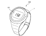
高度計200は、腕時計のように、手首に装着することができる。また、高度計200
の内部には、物理量センサー1(圧力センサー100)が搭載されており、表示部201
に現在地の海抜からの高度、または、現在地の気圧等を表示することができる。
The
Is mounted with a physical quantity sensor 1 (pressure sensor 100) and a
The altitude of the current location from the sea level or the atmospheric pressure of the current location can be displayed.
なお、この表示部201には、現在時刻、使用者の心拍数、天候等、様々な情報を表示
することができる。
The
4.電子機器
次に、本発明の物理量センサーを備える電子機器を適用したナビゲーションシステムに
ついて説明する。図10は、本発明の電子機器の一例を示す正面図である。
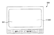
4). Next, a navigation system to which an electronic device including the physical quantity sensor of the present invention is applied will be described. FIG. 10 is a front view showing an example of an electronic apparatus of the present invention.
ナビゲーションシステム300には、図示しない地図情報と、GPS(全地球測位シス
テム:Global Positioning System)からの位置情報取得手段
と、ジャイロセンサーおよび加速度センサーと車速データとによる自立航法手段と、物理
量センサー1と、所定の位置情報または進路情報を表示する表示部301とを備えている
。
The
このナビゲーションシステムによれば、取得した位置情報に加えて高度情報を取得する
ことができる。高度情報を得ることにより、例えば、一般道路と位置情報上は略同一の位
置を示す高架道路を走行する場合、高度情報を持たない場合には、一般道路を走行してい
るのか高架道路を走行しているのかナビゲーションシステムでは判断できず、優先情報と
して一般道路の情報を使用者に提供してしまっていた。そこで、本実施形態に係るナビゲ
ーションシステム300では、高度情報を物理量センサー1によって取得することができ
、一般道路から高架道路へ進入することによる高度変化を検出し、高架道路の走行状態に
おけるナビゲーション情報を使用者に提供することができる。
According to this navigation system, altitude information can be acquired in addition to the acquired position information. By obtaining altitude information, for example, when traveling on an elevated road that shows approximately the same position as a general road, if you do not have altitude information, you are traveling on an ordinary road or on an elevated road The navigation system was unable to determine whether or not the vehicle was being used, and the general road information was provided to the user as priority information. Therefore, in the
なお、表示部301は、例えば液晶パネルディスプレイや、有機EL(Organic Electr
o-Luminescence)ディスプレイなど、小型かつ薄型化が可能な構成となっている。
The
o-Luminescence) display and other devices that can be made smaller and thinner.
なお、本発明の物理量センサーを備える電子機器は、上記のものに限定されず、例えば
、パーソナルコンピューター、携帯電話、医療機器(例えば電子体温計、血圧計、血糖計
、心電図計測装置、超音波診断装置、電子内視鏡)、各種測定機器、計器類(例えば、車
両、航空機、船舶の計器類)、フライトシミュレーター等に適用することができる。
The electronic device provided with the physical quantity sensor of the present invention is not limited to the above-described ones. For example, a personal computer, a mobile phone, a medical device (for example, an electronic thermometer, a blood pressure meter, a blood glucose meter, an electrocardiogram measuring device, an ultrasonic diagnostic device) , Electronic endoscope), various measuring instruments, instruments (for example, vehicles, aircraft, ship instruments), flight simulators, and the like.
5.移動体
次いで、本発明の物理量センサーを適用した移動体(本発明の移動体)について説明す
る。図11は、本発明の移動体の一例を示す斜視図である。
5. Next, the moving body (the moving body of the present invention) to which the physical quantity sensor of the present invention is applied will be described. FIG. 11 is a perspective view showing an example of the moving body of the present invention.
図11に示すように、移動体400は、車体401と、4つの車輪402とを有してお
り、車体401に設けられた図示しない動力源(エンジン)によって車輪402を回転さ
せるように構成されている。このような移動体400には、ナビゲーションシステム30
0(物理量センサー1)が内蔵されている。
As shown in FIG. 11, the moving
0 (physical quantity sensor 1) is built in.
以上、本発明の電子デバイス、物理量センサー、圧力センサー、高度計、電子機器およ
び移動体を図示の各実施形態に基づいて説明したが、本発明はこれらに限定されるもので
はなく、各部の構成は、同様の機能を有する任意の構成のものに置換することができる。
また、他の任意の構成物が付加されていてもよい。
As described above, the electronic device, physical quantity sensor, pressure sensor, altimeter, electronic device, and moving body of the present invention have been described based on the illustrated embodiments, but the present invention is not limited thereto, and the configuration of each part is as follows. It can be replaced with any configuration having a similar function.
Moreover, other arbitrary components may be added.
また、1つのダイヤフラム部に設けられるピエゾ抵抗素子(機能素子)の数は、前述し
た実施形態では4つである場合を例に説明したが、これに限定されず、例えば、1つ以上
3つ以下、または、5つ以上であってもよい。また、ピエゾ抵抗素子の配置や形状等も前
述した実施形態に限定されず、例えば、前述した実施形態において、ダイヤフラム部の中
央部にもピエゾ抵抗素子を配置してもよい。
Moreover, although the number of piezoresistive elements (functional elements) provided in one diaphragm portion has been described as an example in the above-described embodiment, it is not limited to this. For example, one or more three The number may be 5 or less. Further, the arrangement, shape, and the like of the piezoresistive element are not limited to the above-described embodiment. For example, in the above-described embodiment, the piezoresistive element may be arranged at the center of the diaphragm portion.
また、前述した実施形態では、ダイヤフラム部の撓みを検出するセンサー素子としてピ
エゾ抵抗素子を用いた場合を例に説明したが、かかる素子としては、これに限定されず、
例えば、共振子であってもよい。
In the above-described embodiment, the case where a piezoresistive element is used as a sensor element for detecting the deflection of the diaphragm portion has been described as an example, but such an element is not limited to this,
For example, a resonator may be used.
また、前述した実施形態では、本発明の電子デバイスを物理量センサーに適用した場合
を例に説明したが、これに限定されず、前述したように半導体製造プロセスを用いて基板
上に壁部および天井部を形成し、基板、壁部および天井部により内部空間を形成する各種
電子デバイスに本発明を適用することができ、その場合、ダイヤフラム部を省略すること
ができる。
In the above-described embodiment, the case where the electronic device of the present invention is applied to a physical quantity sensor has been described as an example. However, the present invention is not limited to this, and as described above, a wall portion and a ceiling are formed on a substrate using a semiconductor manufacturing process. The present invention can be applied to various electronic devices that form a part and form an internal space by a substrate, a wall part, and a ceiling part. In that case, the diaphragm part can be omitted.
また、前述した実施形態では、壁部の耐蝕層の数が2つの場合を例に説明したが、耐蝕
層の数は、これに限定されず、3つ以上であってもよい。この場合、3つ以上の耐蝕層の
うちの任意の互いに隣り合う2つの耐蝕層により絶縁層を囲んでもよいし、また、3つ以
上の耐蝕層で絶縁層を囲んでもよいが、壁部の基板とは反対側の段差を低減する観点から
、最も天井部側の耐蝕層を含む複数の耐蝕層で絶縁層を囲むことが好ましい。
In the above-described embodiment, the case where the number of the corrosion-resistant layers on the wall portion is two has been described as an example. However, the number of the corrosion-resistant layers is not limited thereto, and may be three or more. In this case, the insulating layer may be surrounded by any two adjacent corrosion-resistant layers among the three or more corrosion-resistant layers, and the insulating layer may be surrounded by three or more corrosion-resistant layers. From the viewpoint of reducing the level difference on the side opposite to the substrate, it is preferable to surround the insulating layer with a plurality of corrosion resistant layers including the corrosion resistant layer on the most ceiling side.
1‥‥物理量センサー
2‥‥基板
3‥‥中間層
5‥‥ピエゾ抵抗素子
5a‥‥ピエゾ抵抗素子
5b‥‥ピエゾ抵抗素子
5c‥‥ピエゾ抵抗素子
5d‥‥ピエゾ抵抗素子
6‥‥積層構造体
20‥‥ダイヤフラム部
21‥‥半導体基板
22‥‥絶縁膜
23‥‥絶縁膜
24‥‥凹部
25‥‥受圧面
41‥‥犠牲層
42‥‥犠牲層
61‥‥層間絶縁膜
62‥‥配線層
63‥‥層間絶縁膜
64‥‥配線層
65‥‥表面保護膜
66‥‥封止層
100‥‥圧力センサー
101‥‥筐体
102‥‥演算部
103‥‥配線
104‥‥貫通孔
200‥‥高度計
201‥‥表示部
211‥‥シリコン層
212‥‥酸化シリコン層
213‥‥シリコン層
214‥‥配線
214a‥‥配線
214b‥‥配線
214c‥‥配線
214d‥‥配線
300‥‥ナビゲーションシステム
301‥‥表示部
400‥‥移動体
401‥‥車体
402‥‥車輪
411‥‥貫通孔
421‥‥貫通孔
621‥‥固定部
622‥‥第1フランジ部
623‥‥第2フランジ部
631‥‥絶縁層
641‥‥被覆層
642‥‥細孔
643‥‥第1接続部
644‥‥第2接続部
645‥‥連結部
651‥‥SiO2層
652‥‥SiN層
P‥‥圧力
S‥‥空洞部
DESCRIPTION OF
Claims (13)
前記基板の一方の面側に配置されている機能素子と、
前記基板の前記一方の面側に前記基板の平面視で前記機能素子を囲んで配置されている
壁部と、
前記壁部に対して前記基板とは反対側に配置されていて、前記壁部とともに内部空間を
構成している天井部と、
を備え、
前記壁部は、絶縁層と、前記絶縁層をエッチング可能なエッチング液に対する耐性が前
記絶縁層よりも高い複数の耐蝕層と、を有し、
前記基板と交差する方向の断面視で、前記複数の耐蝕層が接続して前記絶縁層の周囲に
配置されていることを特徴とする電子デバイス。 A substrate,
A functional element disposed on one side of the substrate;
A wall portion disposed around the functional element in a plan view of the substrate on the one surface side of the substrate;
A ceiling part which is disposed on the opposite side of the substrate with respect to the wall part and constitutes an internal space together with the wall part;
With
The wall portion includes an insulating layer, and a plurality of corrosion-resistant layers having higher resistance to an etchant capable of etching the insulating layer than the insulating layer,
The electronic device, wherein the plurality of corrosion-resistant layers are connected and arranged around the insulating layer in a cross-sectional view in a direction crossing the substrate.
接続していて前記第1耐蝕層とともに前記絶縁層を囲んでいる第2耐蝕層と、を有する請
求項1に記載の電子デバイス。 The plurality of corrosion-resistant layers are connected to the first corrosion-resistant layer and the first corrosion-resistant layer at two locations in the cross-sectional view and surround the insulating layer together with the first corrosion-resistant layer. The electronic device according to claim 1, comprising:
前記基板に固定されている固定部と、
前記固定部から前記内部空間側に延びていて前記基板と離間している第1フランジ部と
、
前記固定部から前記内部空間とは反対側に延びていて前記基板と離間している第2フラ
ンジ部と、
を有し、
前記第2耐蝕層は、
前記第1フランジ部に接続している第1接続部と、
前記第2フランジ部に接続している第2接続部と、
を有する請求項2に記載の電子デバイス。 The first corrosion-resistant layer is
A fixing portion fixed to the substrate;
A first flange portion extending from the fixed portion toward the internal space and spaced apart from the substrate;
A second flange portion extending from the fixed portion to the opposite side of the internal space and spaced from the substrate;
Have
The second corrosion resistant layer is
A first connecting portion connected to the first flange portion;
A second connecting portion connected to the second flange portion;
The electronic device according to claim 2, comprising:
ス。 The electronic device according to claim 1, wherein the corrosion-resistant layer contains a metal.
子デバイス。 The electronic device according to claim 1, wherein the insulating layer contains silicon oxide.
するダイヤフラム部を有する請求項1ないし6のいずれか1項に記載の電子デバイス。 The electronic device according to claim 1, wherein the substrate has a diaphragm portion that is provided at a position overlapping the ceiling portion in a plan view and bends and deforms by receiving pressure.
電子デバイス。 The electronic device according to claim 7, wherein the functional element is a sensor element that outputs an electric signal by distortion.
請求項7に記載の電子デバイス、を備えることを特徴とする物理量センサー。 A physical quantity sensor comprising the electronic device according to claim 7, wherein the functional element is a sensor element disposed on one surface side of the diaphragm portion.
センサー。 A pressure sensor comprising the electronic device according to claim 1.
計。 An altimeter comprising the electronic device according to claim 1.
機器。 An electronic apparatus comprising the electronic device according to claim 1.
体。 A moving body comprising the electronic device according to claim 1.
Priority Applications (3)
| Application Number | Priority Date | Filing Date | Title |
|---|---|---|---|
| JP2014233352A JP2016099114A (en) | 2014-11-18 | 2014-11-18 | Electronic device, physical quantity sensor, pressure sensor, altimeter, electronic apparatus and moving body |
| CN201510784746.0A CN105600735A (en) | 2014-11-18 | 2015-11-16 | Electronic device, physical quantity sensor, pressure sensor, and altimeter |
| US14/943,315 US9682858B2 (en) | 2014-11-18 | 2015-11-17 | Electronic device, physical quantity sensor, pressure sensor, altimeter, electronic apparatus, and moving object |
Applications Claiming Priority (1)
| Application Number | Priority Date | Filing Date | Title |
|---|---|---|---|
| JP2014233352A JP2016099114A (en) | 2014-11-18 | 2014-11-18 | Electronic device, physical quantity sensor, pressure sensor, altimeter, electronic apparatus and moving body |
Publications (2)
| Publication Number | Publication Date |
|---|---|
| JP2016099114A true JP2016099114A (en) | 2016-05-30 |
| JP2016099114A5 JP2016099114A5 (en) | 2017-11-09 |
Family
ID=55961073
Family Applications (1)
| Application Number | Title | Priority Date | Filing Date |
|---|---|---|---|
| JP2014233352A Withdrawn JP2016099114A (en) | 2014-11-18 | 2014-11-18 | Electronic device, physical quantity sensor, pressure sensor, altimeter, electronic apparatus and moving body |
Country Status (3)
| Country | Link |
|---|---|
| US (1) | US9682858B2 (en) |
| JP (1) | JP2016099114A (en) |
| CN (1) | CN105600735A (en) |
Families Citing this family (4)
| Publication number | Priority date | Publication date | Assignee | Title |
|---|---|---|---|---|
| JP6340985B2 (en) * | 2014-08-12 | 2018-06-13 | セイコーエプソン株式会社 | Physical quantity sensor, pressure sensor, altimeter, electronic equipment and moving object |
| JP2016095267A (en) * | 2014-11-17 | 2016-05-26 | セイコーエプソン株式会社 | Electronic device, physical quantity sensor, pressure sensor, altimeter, electronic apparatus and moving body |
| JP2016102737A (en) * | 2014-11-28 | 2016-06-02 | セイコーエプソン株式会社 | Electronic device, physical quantity sensor, pressure sensor, vibrator, altimeter, electronic apparatus and mobile body |
| DE102017218883A1 (en) * | 2017-10-23 | 2019-04-25 | Fraunhofer-Gesellschaft zur Förderung der angewandten Forschung e.V. | Microelectromechanical component and a method for its production |
Citations (4)
| Publication number | Priority date | Publication date | Assignee | Title |
|---|---|---|---|---|
| US20110209555A1 (en) * | 2010-03-01 | 2011-09-01 | Marcus Ahles | Micromechanical pressure-sensor element and method for its production |
| JP2012096316A (en) * | 2010-11-02 | 2012-05-24 | Seiko Epson Corp | Electronic device and method for manufacturing electronic device |
| JP2014086447A (en) * | 2012-10-19 | 2014-05-12 | Seiko Epson Corp | Electronic apparatus and manufacturing method of the same |
| JP2014115209A (en) * | 2012-12-11 | 2014-06-26 | Seiko Epson Corp | Mems element, electronic device, altimeter, electronic apparatus and moving body |
Family Cites Families (5)
| Publication number | Priority date | Publication date | Assignee | Title |
|---|---|---|---|---|
| US20070013014A1 (en) * | 2005-05-03 | 2007-01-18 | Shuwen Guo | High temperature resistant solid state pressure sensor |
| JP2008114354A (en) | 2006-11-08 | 2008-05-22 | Seiko Epson Corp | Electronic device and its manufacturing method |
| JP5630243B2 (en) | 2010-11-30 | 2014-11-26 | セイコーエプソン株式会社 | Electronic device, electronic apparatus, and method of manufacturing electronic device |
| JP2014057125A (en) * | 2012-09-11 | 2014-03-27 | Seiko Epson Corp | Electronic device, method of manufacturing the same, and oscillator |
| JP2014192435A (en) * | 2013-03-28 | 2014-10-06 | Seiko Epson Corp | Electronic device, method of manufacturing the same, and oscillator |
-
2014
- 2014-11-18 JP JP2014233352A patent/JP2016099114A/en not_active Withdrawn
-
2015
- 2015-11-16 CN CN201510784746.0A patent/CN105600735A/en active Pending
- 2015-11-17 US US14/943,315 patent/US9682858B2/en active Active
Patent Citations (4)
| Publication number | Priority date | Publication date | Assignee | Title |
|---|---|---|---|---|
| US20110209555A1 (en) * | 2010-03-01 | 2011-09-01 | Marcus Ahles | Micromechanical pressure-sensor element and method for its production |
| JP2012096316A (en) * | 2010-11-02 | 2012-05-24 | Seiko Epson Corp | Electronic device and method for manufacturing electronic device |
| JP2014086447A (en) * | 2012-10-19 | 2014-05-12 | Seiko Epson Corp | Electronic apparatus and manufacturing method of the same |
| JP2014115209A (en) * | 2012-12-11 | 2014-06-26 | Seiko Epson Corp | Mems element, electronic device, altimeter, electronic apparatus and moving body |
Also Published As
| Publication number | Publication date |
|---|---|
| US20160137494A1 (en) | 2016-05-19 |
| US9682858B2 (en) | 2017-06-20 |
| CN105600735A (en) | 2016-05-25 |
Similar Documents
| Publication | Publication Date | Title |
|---|---|---|
| US9891125B2 (en) | Electronic device, physical quantity sensor, pressure sensor, vibrator, altimeter, electronic apparatus, and moving object | |
| US9631992B2 (en) | Physical quantity sensor, pressure sensor, altimeter, electronic apparatus and moving object | |
| US9683907B2 (en) | Physical quantity sensor, altimeter, electronic apparatus, and moving object | |
| JP2016102768A (en) | Electronic device, physical quantity sensor, pressure sensor, vibrator, altimeter, electronic apparatus and mobile body | |
| US20160138990A1 (en) | Electronic Device, Physical Quantity Sensor, Pressure Sensor, Altimeter, Electronic Apparatus, And Moving Object | |
| US20150217989A1 (en) | Mems device, pressure sensor, altimeter, electronic apparatus, and moving object | |
| US20160033347A1 (en) | Physical quantity sensor, pressure sensor, altimeter, electronic device, and moving object | |
| JP2016095284A (en) | Electronic device, physical quantity sensor, pressure sensor, altimeter, electronic apparatus and movable body | |
| JP6340985B2 (en) | Physical quantity sensor, pressure sensor, altimeter, electronic equipment and moving object | |
| US20150268114A1 (en) | Physical quantity sensor, method for manufacturing physical quantity sensor, pressure sensor, altimeter, electronic device, and moving object | |
| US20150219515A1 (en) | Physical quantity sensor, altimeter, electronic apparatus, and moving object | |
| US9682858B2 (en) | Electronic device, physical quantity sensor, pressure sensor, altimeter, electronic apparatus, and moving object | |
| US9207137B2 (en) | Physical quantity sensor, pressure sensor, altimeter, electronic apparatus, and moving object | |
| US9856138B2 (en) | Electronic device, pressure sensor, altimeter, electronic apparatus, and moving object | |
| JP2016102693A (en) | Electronic device, physical quantity sensor, pressure sensor, vibrator, altimeter, electronic apparatus and mobile body | |
| JP2016099302A (en) | Physical quantity sensor, pressure sensor, altimeter, electronic apparatus and moving body | |
| JP2016138794A (en) | Electronic device, method for manufacturing electronic device, pressure sensor, vibrator, altimeter, electronic apparatus, and mobile body | |
| JP2015125045A (en) | Physical quantity sensor, pressure sensor, altimeter, electronic apparatus, and movable body | |
| JP2016200534A (en) | Electronic device, pressure sensor, altimeter, electronic apparatus, and mobile body | |
| JP2015179000A (en) | Physical amount sensor, altimeter, electronic equipment, and traveling object | |
| JP2015141107A (en) | Physical quantity sensor, manufacturing method of the same, pressure sensor, altimeter, electronic apparatus and movable body | |
| JP2016095270A (en) | Physical quantity sensor, pressure sensor, altimeter, electronic apparatus and movable body | |
| JP2016031278A (en) | Physical quantity sensor, pressure sensor, altimeter, electronic device, and moving object | |
| JP2016031279A (en) | Physical quantity sensor, pressure sensor, altimeter, electronic device, and moving object | |
| JP2016030311A (en) | Method for manufacturing physical quantity sensor, physical quantity sensor, pressure sensor, altimeter, electronic equipment, and mobile |
Legal Events
| Date | Code | Title | Description |
|---|---|---|---|
| RD03 | Notification of appointment of power of attorney |
Free format text: JAPANESE INTERMEDIATE CODE: A7423 Effective date: 20160623 |
|
| A521 | Request for written amendment filed |
Free format text: JAPANESE INTERMEDIATE CODE: A523 Effective date: 20170927 |
|
| A621 | Written request for application examination |
Free format text: JAPANESE INTERMEDIATE CODE: A621 Effective date: 20170927 |
|
| A977 | Report on retrieval |
Free format text: JAPANESE INTERMEDIATE CODE: A971007 Effective date: 20180711 |
|
| A131 | Notification of reasons for refusal |
Free format text: JAPANESE INTERMEDIATE CODE: A131 Effective date: 20180724 |
|
| RD05 | Notification of revocation of power of attorney |
Free format text: JAPANESE INTERMEDIATE CODE: A7425 Effective date: 20180905 |
|
| A761 | Written withdrawal of application |
Free format text: JAPANESE INTERMEDIATE CODE: A761 Effective date: 20180925 |