JP2016029748A - Method for manufacturing shield printed wiring board - Google Patents
Method for manufacturing shield printed wiring board Download PDFInfo
- Publication number
- JP2016029748A JP2016029748A JP2015235803A JP2015235803A JP2016029748A JP 2016029748 A JP2016029748 A JP 2016029748A JP 2015235803 A JP2015235803 A JP 2015235803A JP 2015235803 A JP2015235803 A JP 2015235803A JP 2016029748 A JP2016029748 A JP 2016029748A
- Authority
- JP
- Japan
- Prior art keywords
- shield
- shield film
- insulating layer
- film
- resin
- Prior art date
- Legal status (The legal status is an assumption and is not a legal conclusion. Google has not performed a legal analysis and makes no representation as to the accuracy of the status listed.)
- Pending
Links
Images


Abstract
Description
本発明は、電子機器などの装置内等において用いられるシールドプリント配線板の製造方法に関する。 The present invention relates to a method for manufacturing a shield printed wiring board used in an apparatus such as an electronic device.
従来から、電磁波などのノイズを遮蔽するシールドフィルムが公知である。例えば、特許文献1には、プリント回路を含む基体フィルム上に、シールドフィルムを被覆するに際し、カバーフィルムの片面にシールド層を設け、他面に剥離可能な粘着性を有する粘着性フィルムを貼り合わせて補強シールドフィルムを形成し、前記基体フィルム上に前記シールド層が当接するように前記補強シールドフィルムを載置し、加熱・加圧して接着させた後、前記粘着性フィルムを剥離するシールドフレキシブルプリント配線板の製造方法、が開示されている。
Conventionally, shield films that shield noise such as electromagnetic waves are known. For example, in
上記従来のシールドフィルムにおけるカバーフィルム(絶縁層)は、粘着性フィルム(保護層)と呼ばれるPET(ポリエチレンテレフタレート)フィルムを基体として、液状の樹脂が薄く塗布されて形成される。このようなカバーフィルムは、プリント配線板との加熱プレス工程が行われる前の状態、即ちシールドフィルム単体としては、所謂Bステージと言われるような半硬化状態までに重合の進行が留められることが一般的である。 The cover film (insulating layer) in the conventional shield film is formed by thinly applying a liquid resin using a PET (polyethylene terephthalate) film called an adhesive film (protective layer) as a base. In such a cover film, the progress of the polymerization may be stopped until the state before the heating press process with the printed wiring board is performed, that is, as the shield film alone, a semi-cured state called a so-called B stage. It is common.
このように、カバーフィルムは、加熱プレス工程前のシールドフィルム単体としては半硬化状態であるため粘着性フィルムとの接着力が高く、粘着性フィルムから剥離できない状態となっている。また、粘着性フィルムは、カバーフィルムや金属薄膜層を積層する際の基体としての機能や、加熱プレス工程でカバーフィルムを保護する機能や、シールドフィルムの運送時・保管時においての半硬化状態のカバーフィルムを保護する機能を担っている。このため、シールドフィルム単体において、粘着性フィルムはカバーフィルムに必ず積層されるものである。 Thus, since the cover film is in a semi-cured state as the shield film alone before the heat press step, the cover film has a high adhesive force with the adhesive film and cannot be peeled off from the adhesive film. In addition, the adhesive film has a function as a base when laminating a cover film and a metal thin film layer, a function to protect the cover film in a heating press process, and a semi-cured state when the shield film is transported and stored. It is responsible for protecting the cover film. For this reason, in the shield film alone, the adhesive film is necessarily laminated on the cover film.
また、上記のようなシールドフィルムの粘着性フィルム側の面、又は、この粘着性フィルムとは反対側の面に、さらに保護部材が積層され、この保護部材を残すようにシールドフィルムをハーフカットすることが一般的に行われている。これにより、保護部材上に所望の形状に切断されたシールドフィルムが積層された状態となり、加熱プレス工程前にはこのようなシールドフィルムを保護部材上から剥離しプリント配線板に載置することができる。 Further, a protective member is further laminated on the adhesive film side surface of the shield film as described above or on the surface opposite to the adhesive film, and the shield film is half-cut so as to leave this protective member. It is generally done. As a result, a shield film cut into a desired shape is laminated on the protective member, and such a shield film can be peeled off from the protective member and placed on the printed wiring board before the heat pressing step. it can.
しかしながら、特許文献1のような従来の方法でシールドプリント配線板を製造する場合、プリント基板との加熱プレスによりカバーフィルムを硬化させることで粘着性フィルムとカバーフィルムとの接着力を低下させた後に、カバーフィルムから粘着性フィルムを剥離する必要があるため、プリント基板に圧着されたシールドフィルムから粘着性フィルムを剥離する工程が必要であった。さらに、近年シールドフィルムは圧着されるプリント基板と共に小型化が進んでいるため、プリント基板と圧着されたシールドフィルムから粘着性フィルムを剥離する工程は手間が掛かるものであり、コストを増大させる要因となっていた。
また、粘着性フィルムであるPETは高温(たとえば200℃)、長時間および複数回プレスの場合、PETが劣化して剥がせなくなるという問題点もあった。
However, when manufacturing a shield printed wiring board by the conventional method like
In addition, PET, which is an adhesive film, has a problem in that when it is pressed at a high temperature (for example, 200 ° C.) for a long time and a plurality of times, the PET deteriorates and cannot be removed.
そこで、本発明は、コストを削減することができるシールドプリント配線板の製造方法を提供することを目的とする。 Then, an object of this invention is to provide the manufacturing method of the shield printed wiring board which can reduce cost.
本発明のシールドプリント配線板の製造方法は、樹脂硬化度が90%以上になるまで重合が進行した樹脂である絶縁層と、前記絶縁層に積層されたシールド層と、前記シールド層に積層された接着剤層とを有するシールドフィルムを形成する工程と、前記シールドフィルムをプリント基板に載置する工程と、前記シールドフィルムと前記プリント基板とを加熱プレスする工程とを備え、前記シールドフィルムを形成する工程は、前記絶縁層側の面が保護部材に当接するように当該保護部材に積層された前記シールドフィルムを、前記接着剤層側から前記保護部材を残して前記積層体を切断するハーフカット工程と、切断された前記シールドフィルムを前記保護部材から剥離する工程とを備えたことを特徴とする。 The method for producing a shield printed wiring board according to the present invention includes an insulating layer that is a resin that has undergone polymerization until the degree of resin cure is 90% or more, a shield layer that is laminated on the insulating layer, and a laminate that is laminated on the shield layer. Forming a shield film having an adhesive layer, a step of placing the shield film on a printed circuit board, and a step of heat pressing the shield film and the printed circuit board to form the shield film. The step of cutting the shield film laminated on the protective member so that the surface on the insulating layer side is in contact with the protective member, and cutting the laminate from the adhesive layer side leaving the protective member And a step of peeling the cut shield film from the protective member.
また、本発明のシールドプリント配線板の製造方法は、樹脂硬化度が90%以上になるまで重合が進行した樹脂である絶縁層と、前記絶縁層に積層された等方導電性接着剤層とを有するシールドフィルムを形成する工程と、前記シールドフィルムをプリント基板に載置する工程と、前記シールドフィルムと前記プリント基板とを加熱プレスする工程とを備え、前記シールドフィルムを形成する工程は、前記絶縁層側の面が保護部材に当接するように当該保護部材に積層された前記シールドフィルムを、前記接着剤層側から前記保護部材を残して前記積層体を切断するハーフカット工程と、切断された前記シールドフィルムを前記保護部材から剥離する工程とを備えたことを特徴とする。 The method for producing a shielded printed wiring board according to the present invention includes an insulating layer that is a resin that has undergone polymerization until the resin curing degree is 90% or more, and an isotropic conductive adhesive layer that is laminated on the insulating layer. A step of forming the shield film, a step of placing the shield film on a printed circuit board, and a step of heat-pressing the shield film and the printed circuit board, and the step of forming the shield film includes the steps of: The shield film laminated on the protective member so that the surface on the insulating layer side is in contact with the protective member, and the half cut step of cutting the laminated body leaving the protective member from the adhesive layer side. And a step of peeling the shield film from the protective member.
上記構成によれば、絶縁層は樹脂硬化度が90%以上になるまで重合が進行した樹脂で形成されている。これにより、硬化状態にされた絶縁層は、導電層を積層する際の基体としての機能等の従来の保護層の機能を備えるため、シールドフィルムとして保護層が不要となる。その結果、加熱プレス工程後において、シールドプリント配線板のシールドフィルムから保護層を剥離する工程を不要とすることができ、コストを削減することができる。
さらに、保護部材に積層されたシールドフィルムがハーフカットされ、切断されたシールドフィルムを剥離してプリント基板に載置することができる。これにより、プリント基板に適した形状のシールドフィルムを形成することができると共に、このようなシールドフィルムを保護部材上で保管することができる。
According to the said structure, the insulating layer is formed with resin which superposition | polymerization progressed until the resin cure degree became 90% or more. As a result, the cured insulating layer has the function of a conventional protective layer such as a function as a base when laminating the conductive layers, and thus a protective layer is unnecessary as a shield film. As a result, it is possible to eliminate the step of peeling the protective layer from the shield film of the shield printed wiring board after the heat pressing step, and the cost can be reduced.
Furthermore, the shield film laminated | stacked on the protection member is half-cut, the cut | disconnected shield film can be peeled, and it can mount in a printed circuit board. Thereby, while being able to form the shield film of a shape suitable for a printed circuit board, such a shield film can be stored on a protection member.
また、本発明のシールドプリント配線板の製造方法は、樹脂硬化度が90%以上になるまで重合が進行した樹脂である絶縁層と、前記絶縁層に積層されたシールド層と、前記シールド層に積層された接着剤層とを有するシールドフィルムを形成する工程と、前記シールドフィルムをプリント基板に載置する工程と、前記シールドフィルムと前記プリント基板とを加熱プレスする工程とを備え、前記シールドフィルムを形成する工程は、前記シールドフィルムを、前記絶縁層側の面が保護シート(シート状のゴム、樹脂など)に当接するように当該保護シートに載置して当該積層体を切断するカット工程を備えたことを特徴とする。 The method for producing a shielded printed wiring board according to the present invention includes an insulating layer that is a resin that has undergone polymerization until the resin curing degree is 90% or more, a shield layer that is laminated on the insulating layer, and a shield layer. A step of forming a shield film having a laminated adhesive layer, a step of placing the shield film on a printed board, and a step of heat pressing the shield film and the printed board. A step of cutting the laminate by placing the shield film on the protective sheet such that the surface on the insulating layer side is in contact with the protective sheet (sheet-like rubber, resin, etc.) It is provided with.
また、本発明のシールドプリント配線板の製造方法は、樹脂硬化度が90%以上になるまで重合が進行した樹脂である絶縁層と、前記絶縁層に積層された等方導電性接着剤層とを有するシールドフィルムを形成する工程と、前記シールドフィルムをプリント基板に載置する工程と、前記シールドフィルムと前記プリント基板とを加熱プレスする工程とを備え、前記シールドフィルムを形成する工程は、前記シールドフィルムを、前記絶縁層側の面が保護シートに当接するように当該保護シートに載置して当該積層体を切断するカット工程を備えたことを特徴とする。 The method for producing a shielded printed wiring board according to the present invention includes an insulating layer that is a resin that has undergone polymerization until the resin curing degree is 90% or more, and an isotropic conductive adhesive layer that is laminated on the insulating layer. A step of forming the shield film, a step of placing the shield film on a printed circuit board, and a step of heat-pressing the shield film and the printed circuit board, and the step of forming the shield film includes the steps of: It is characterized by comprising a cutting step of placing the shield film on the protective sheet so that the surface on the insulating layer side is in contact with the protective sheet and cutting the laminate.
上記構成によれば、絶縁層は樹脂硬化度が90%以上になるまで重合が進行した樹脂で形成されている。これにより、硬化状態にされた絶縁層は、導電層を積層する際の基体としての機能等の従来の保護層の機能を備えるため、シールドフィルムとして保護層が不要となる。その結果、加熱プレス工程後において、シールドプリント配線板のシールドフィルムから保護層を剥離する工程を不要とすることができ、コストを削減することができる。さらに、シールドフィルムが保護シート上でカットされ、切断されたシールドフィルムをプリント配線板に載置することができる。これにより、プリント基板に適した形状のシールドフィルムを形成することができる。 According to the said structure, the insulating layer is formed with resin which superposition | polymerization progressed until the resin cure degree became 90% or more. As a result, the cured insulating layer has the function of a conventional protective layer such as a function as a base when laminating the conductive layers, and thus a protective layer is unnecessary as a shield film. As a result, it is possible to eliminate the step of peeling the protective layer from the shield film of the shield printed wiring board after the heat pressing step, and the cost can be reduced. Furthermore, the shield film is cut on the protective sheet, and the cut shield film can be placed on the printed wiring board. Thereby, the shield film of the shape suitable for a printed circuit board can be formed.
また、本発明のシールドプリント配線板の製造方法において、前記絶縁層は、フィルム状に形成されていてもよい。
上記構成によれば、絶縁層はフィルム状に形成されている。これにより、絶縁層は伸縮しやすいため、凹凸のあるプリント基板に加熱プレスを行った場合でも、絶縁層に破断が生じにくいものとなる。
Moreover, in the manufacturing method of the shield printed wiring board of this invention, the said insulating layer may be formed in the film form.
According to the said structure, the insulating layer is formed in the film form. As a result, the insulating layer easily expands and contracts, so that the insulating layer is unlikely to break even when heat pressing is performed on a printed board with unevenness.
また、本発明のシールドプリント配線板の製造方法において、前記絶縁層は、耐熱性樹脂で形成されていてもよい。
上記構成によれば、絶縁層が耐熱性樹脂で形成されているため、加熱プレス工程における耐性を向上させることができる。
Moreover, in the manufacturing method of the shield printed wiring board of this invention, the said insulating layer may be formed with heat resistant resin.
According to the said structure, since the insulating layer is formed with the heat resistant resin, the tolerance in a heat press process can be improved.
また、本発明のシールドプリント配線板の製造方法において、前記絶縁層は、層厚が2μm〜25μmに形成されていてもよい。 上記構成によれば、層厚が2μm〜25μmに形成されているため、加熱プレス工程においてプリント基板に対するシールドフィルムの接着剤層の埋め込み性を向上することができる。 Moreover, in the manufacturing method of the shield printed wiring board of this invention, the said insulating layer may be formed in 2 micrometers-25 micrometers in layer thickness. According to the said structure, since the layer thickness is formed in 2 micrometers-25 micrometers, the embedding property of the adhesive bond layer of the shield film with respect to a printed circuit board in a heat press process can be improved.
以下、本発明の好適な実施の形態について、図面を参照しつつ説明する。 Hereinafter, preferred embodiments of the present invention will be described with reference to the drawings.
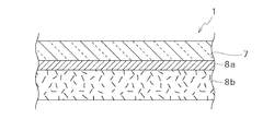
(シールドフィルム1の構成)
図1に示すように、シールドフィルム1は、樹脂硬化度が90%以上になるまで重合が進行した樹脂である絶縁層7と、絶縁層に積層されたシールド層としての金属層8aと、金属層8aに積層された接着剤層8bとを有している。
(Configuration of shield film 1)
As shown in FIG. 1, the
ここで、樹脂硬化度とは、樹脂の硬化反応の進行の度合い(反応率)を示すものである。樹脂硬化度は、未反応材料が0%であり、反応後材料が100%である。樹脂硬化度は、例えば、FT−IR(フーリエ変換型赤外分光)スペクトルによる樹脂硬化度の測定値から得ることができ、FT−IR装置によって対象の樹脂に赤外線を照射し、透過又は分光させてスペクトルを得ることで硬化反応の進行を測定することが可能である。具体的には、未反応材料と、100%反応後材料と、測定対象の樹脂のスペクトルを比較し最も顕著な違いがみられる領域を確定し、当該領域での各試料のピーク強度を比較することで樹脂硬化度を求めることができる。
尚、樹脂硬化度の測定はFT−IRを用いたものに限定されず、分散型赤外分光光度計等を用いてもよい。
Here, the resin curing degree indicates the degree of progress of the resin curing reaction (reaction rate). The degree of resin curing is 0% for unreacted material and 100% for post-reaction material. The resin curing degree can be obtained from, for example, a measurement value of the resin curing degree by an FT-IR (Fourier transform infrared spectroscopy) spectrum, and the target resin is irradiated with infrared rays to be transmitted or dispersed. Thus, it is possible to measure the progress of the curing reaction by obtaining a spectrum. Specifically, by comparing the spectrum of the resin to be measured with the unreacted material, the 100% post-reaction material, the region where the most remarkable difference is observed is determined, and the peak intensity of each sample in the region is compared. Thus, the degree of resin curing can be obtained.
The measurement of the resin curing degree is not limited to the one using FT-IR, and a dispersion type infrared spectrophotometer or the like may be used.
また、図1に図示しないが、シールドフィルム1は、プリント基板等への加熱プレス工程の前には、保護部材に貼り付けられた状態にされていてもよい。
Although not shown in FIG. 1, the
(絶縁層7)
絶縁層7は樹脂硬化度が90%以上になるまで重合が進行した樹脂で形成されている。尚、硬化形態としては、熱硬化、紫外線硬化、電子線硬化などどれでもよく、重合が進行されて硬化するものであればよい。熱硬化性樹脂としては、例えば、フェノール樹脂、アクリル樹脂、エポキシ樹脂、メラミン樹脂、シリコン樹脂、アクリル変性シリコン樹脂などが挙げられる。また、紫外線硬化性樹脂としては、例えば、エポキシアクリレート樹脂、ポリエステルアクリレート樹脂、及びそれらのメタクリレート変性品などが挙げられる。
(Insulating layer 7)
The insulating
また、絶縁層7は、耐熱性を有する樹脂で形成されることが好ましく、例えば、ポリイミドを用いることが好ましい。これにより、複数回や長時間の加熱プレスに耐え得る。また、ポリイミドよりも低い吸水率を有する熱可塑性ポリイミドを用いることがさらに好ましい。これにより、シールドプリント配線板へのリフロー処理などにおいて、絶縁層の膨れを防止することができる。
尚、絶縁層7は、上記樹脂に限定されず、耐熱性樹脂として、例えば、架橋ポリエチレン、ポリベンツイミダゾール、アラミド、ポリイミドアミド、ポリエーテルイミド、ポリフェニレンサルファイド(PPS)、ポリエチレンナフタレート(PEN)などの樹脂を用いてもよい。
The insulating
The insulating
絶縁層7は、フィルム状に形成された絶縁樹脂が用いられることが好ましい。これにより、絶縁層7が伸縮しやすいものとなるため、凹凸のあるプリント配線板に加熱プレスを行った場合でも、絶縁層7が凹凸形状に追従しやすいため破断が生じにくくなる。尚、絶縁層7は、フィルム状の絶縁樹脂に限定されず、基体となるフィルム上に絶縁樹脂がコーティングされることにより成層されたコーティング層であってもよい。絶縁層7が、このようなコーティング層である場合でも、プリント配線板との加熱プレス前に基体となるフィルムを常温で剥離することができるので、加熱プレス前に保護層が剥離されたシールドフィルムを製造でき、加熱プレス後にシールドプリント配線板から保護層を剥離する工程が不要になる。
The insulating
絶縁層7の厚みの下限は、2μmが好ましく、4μmがより好ましい。また、絶縁層7の厚みの上限は、25μmが好ましく、12μmがより好ましく、8μmがさらに好ましい。
The lower limit of the thickness of the insulating
絶縁層7は、上記のような樹脂に、着色用の顔料等が含まれているものであってもよい。例えば、カーボンブラック等を挙げることができる。また、絶縁層7は、外側表面がマット処理されていてもよい。マット処理は、エンボスロール加工、練りこみマット、ケミカルマットコートおよびサンドブラスト加工等のいずれで行われるものであってもよい。
The insulating
絶縁層7は、単層構造に限定されるものではなく、複数層構造であってもよい。例えば、耐摩耗性・耐ブロッキング性に優れた樹脂からなるハード層とクッション性に優れた樹脂からなるソフト層とを順次コーティングすることによって形成した2層構造であってもよい。
The insulating
(金属層8a)
金属層8aは、圧延加工により形成されることが好ましい。これにより、シールドフィルム1は良好な形状保持性を有するとともに、凹凸のあるプリント配線板に加熱プレスを行った場合のシールドフィルム1の追従性を良好にすることができる。尚、金属層8aは、これに限定されず、真空蒸着、電解めっき法、無電解めっき法、スパッタリング法、電子ビーム蒸着法、真空蒸着法、CVD法、メタルオーガニックなどにより形成された金属薄膜であってもよい。
また、金属層8aは、特殊電解めっき法によって、金属箔と同様に結晶が面方向に広がった構造を有するように形成された金属薄膜であってもよい。これにより、圧延加工と同様に、良好な形状保持性を得ることができる。
(
The
Moreover, the
金属層8aを形成する金属材料としては、ニッケル、銅、銀、錫、金、パラジウム、アルミニウム、クロム、チタン、亜鉛、及び、これらの材料の何れか1つ以上を含む合金などを挙げることができる。尚、金属層8aの材料は、特に銀が好ましい。これにより、層厚が薄くてもシールド特性を確保することができる。
Examples of the metal material for forming the
尚、金属層8aの厚みの下限は、0.01μmが好ましく、0.1μmがより好ましく、また、金属層8aの厚みの上限は、18μmが好ましく、12μmがより好ましく、6μmが更に好ましい。また、金属層8aは、単層構造に限定されるものではなく、複数層構造であってもよい。
The lower limit of the thickness of the
(接着剤層8b)
接着剤層8bは、接着性樹脂に導電性フィラーが添加されて形成される導電性接着剤で成層されている。シールドプリント配線板は、グランド用配線パターン及び信号用配線パターンが形成されたベース部材と、ベース部材上に積層されると共にグランド用配線パターンの少なくとも一部を露出する絶縁フィルムと、を有するプリント配線板にシールドフィルムを貼りあわせ加熱プレスされて形成される。シールドフィルム1はプリント配線板との貼りあわせ面に接着剤層8bを有しているため、加熱プレス時に絶縁フィルムのグランド用配線パターンが露出される箇所に埋め込まれる。このように、接着剤層8bを設けることで確実にプリント配線板のグランド回路と金属層8aとを電気的に接続できる。尚、接着剤層8bは、導電性接着剤で形成されることに限定されず、導電性を有しない接着性樹脂で形成されるものであってもよい。
(
The
接着性樹脂としては、ポリスチレン系、酢酸ビニル系、ポリエステル系、ポリエチレン系、ポリプロピレン系、ポリアミド系、ゴム系、アクリル系などの熱可塑性樹脂や、フェノール系、エポキシ系、ウレタン系、メラミン系、アルキッド系などの熱硬化性樹脂で構成されている。耐熱性が特に要求されない場合は、保管条件等に制約を受けないポリエステル系の熱可塑性樹脂が望ましく、耐熱性もしくはより優れた可撓性が要求される場合においては、信頼性の高いエポキシ系の熱硬化性樹脂が望ましい。 Adhesive resins include thermoplastic resins such as polystyrene, vinyl acetate, polyester, polyethylene, polypropylene, polyamide, rubber, and acrylic, phenolic, epoxy, urethane, melamine, and alkyd. It is composed of a thermosetting resin such as a system. When heat resistance is not particularly required, a polyester-based thermoplastic resin that is not restricted by storage conditions or the like is desirable. When heat resistance or better flexibility is required, a highly reliable epoxy resin is required. A thermosetting resin is desirable.
導電性フィラーとしては、カーボン、銀、銅、ニッケル、ハンダ、アルミ及び銅粉に銀メッキを施した銀コート銅フィラー、さらには樹脂ボールやガラスビーズ等に金属メッキを施したフィラー又はこれらのフィラーの混合体が用いられる。銀は高価であり、銅は耐熱の信頼性に欠け、アルミは耐湿の信頼性に欠け、さらにハンダは十分な導電性を得ることが困難であることから、比較的安価で優れた導電性を有し、さらに信頼性の高い銀コート銅フィラー又はニッケルを用いるのが好ましい。 Examples of the conductive filler include silver-coated copper filler obtained by silver-plating carbon, silver, copper, nickel, solder, aluminum, and copper powder, and fillers obtained by metal-plating resin balls, glass beads, or the like. A mixture of Silver is expensive, copper lacks heat resistance reliability, aluminum lacks moisture resistance reliability, and solder is difficult to obtain sufficient conductivity. It is preferable to use a silver-coated copper filler or nickel having high reliability.
また、導電性接着剤として、導電性フィラーの量を少なくした異方導電性接着剤を使用してもよい。このように、導電性接着剤として異方導電性接着剤を使用すると、等方導電性接着剤よりも薄膜になり、導電性フィラーの量が少ないため、可撓性の優れたものにすることができる。また、導電性接着剤として、等方導電性接着剤を使用することもできる。このように、導電性接着剤として、等方導電性接着剤を使用すると、等方導電性接着剤による導電性接着剤層を設けるだけで、グランド回路等に対するグランド接続を可能とするとともに電磁波シールド効果を持たせることができるので、シールド層と接着剤層の役目を果たすことができる。この場合、金属層を省いてもよい。 Moreover, you may use the anisotropic conductive adhesive which reduced the quantity of the conductive filler as a conductive adhesive. As described above, when an anisotropic conductive adhesive is used as the conductive adhesive, the film becomes thinner than the isotropic conductive adhesive, and the amount of the conductive filler is small. Can do. Moreover, an isotropic conductive adhesive can also be used as a conductive adhesive. As described above, when an isotropic conductive adhesive is used as the conductive adhesive, the ground connection to the ground circuit or the like can be achieved and the electromagnetic wave shield only by providing the conductive adhesive layer with the isotropic conductive adhesive. Since an effect can be given, it can serve as a shield layer and an adhesive layer. In this case, the metal layer may be omitted.
また、接着剤層8bに導電性接着剤を用いる場合、金属フィラー等の導電性フィラーの接着性樹脂への配合割合は、フィラーの形状等にも左右されるが、接着性樹脂100重量部に対して、下限は10重量部とするのが好ましく、上限は400重量部とするのが好ましい。
また、接着剤層8bに異方導電性接着剤を用いる場合、導電性フィラーの接着性樹脂への配合割合は、接着性樹脂100重量部に対して下限は10重量部とするのが好ましく、上限は180重量部とするのが好ましい。また、接着剤層8bに等方導電性接着剤を用いる場合、導電性フィラーの接着性樹脂への配合割合は、接着性樹脂100重量部に対して下限は150重量部とするのが好ましく、上限は250重量部とするのが好ましい。
導電性フィラーとして銀コート銅フィラーを用いる場合は、接着性樹脂100重量部に対して下限は10重量部とするのが好ましく、さらに好ましくは20重量部とするのがよい。また、上限は400重量部とするのが好ましく、さらに好ましくは150重量部とするのがよい。銀コート銅フィラーを用いた場合に400重量部を超えると、グランド回路への接着性が低下し、シールドフィルム1の可撓性が悪くなる。また、10重量部を下回ると導電性が著しく低下する。
導電性フィラーとしてニッケルフィラーを用いる場合は、接着性樹脂100重量部に対して下限は40重量部とするのが好ましく、さらに好ましくは100重量部とするのがよい。また、上限は400重量部とするのが好ましく、さらに好ましくは350重量部とするのがよい。ニッケルフィラーを用いた場合に400重量部を超えると、グランド回路への接着性が低下し、シールドフィルム1の可撓性が悪くなる。また、40重量部を下回ると導電性が著しく低下する。
尚、金属フィラー等の導電性フィラーの形状は、球状、針状、繊維状、フレーク状、樹枝状のいずれであってもよい。
In addition, when a conductive adhesive is used for the
When using an anisotropic conductive adhesive for the
When a silver-coated copper filler is used as the conductive filler, the lower limit is preferably 10 parts by weight, more preferably 20 parts by weight with respect to 100 parts by weight of the adhesive resin. The upper limit is preferably 400 parts by weight, and more preferably 150 parts by weight. If the silver-coated copper filler is used in excess of 400 parts by weight, the adhesion to the ground circuit is lowered and the flexibility of the
When a nickel filler is used as the conductive filler, the lower limit is preferably 40 parts by weight, more preferably 100 parts by weight with respect to 100 parts by weight of the adhesive resin. The upper limit is preferably 400 parts by weight, more preferably 350 parts by weight. When the nickel filler is used and exceeds 400 parts by weight, the adhesion to the ground circuit is lowered and the flexibility of the
The shape of the conductive filler such as a metal filler may be any of a spherical shape, a needle shape, a fiber shape, a flake shape, and a dendritic shape.
接着剤層8bの厚さは、導電性接着剤を用いるか否かによらず3〜25μmが好ましい。尚、これに限定されず、接着剤層8bは、金属フィラー等の導電性フィラーを混合した分だけ厚くなってもよい。また、導電性フィラーを混合しない場合は、薄くすることが可能となる。
The thickness of the
このように、シールドフィルム1は、絶縁層が樹脂硬化度が90%以上になるまで重合が進行した樹脂で形成されているため導電層を積層する際の基体としての機能等の従来の保護層の機能を備える。従って、保護層を有しないシールドフィルム1を形成することが可能であるため、加熱プレス工程後において、シールドプリント配線板のシールドフィルムから保護層を剥離する工程を不要とすることができ、コストを削減することができる。
また、一般的に絶縁層、シールド層及び接着剤層を合わせた層厚よりも厚く50μm程度に形成されていた保護層が不要であるため、シールドフィルムを巻回等して保管や移送する場合のコスト削減を図ることができる。
Thus, since the
In addition, since a protective layer that is generally thicker than the combined thickness of the insulating layer, shield layer, and adhesive layer and is formed to about 50 μm is unnecessary, the shield film is wound and stored or transported. Cost reduction.
(シールドプリント配線板10の製造方法)
上記のようなシールドフィルム1を用いたシールドプリント配線板10の製造方法について説明する。
(Method for manufacturing shield printed wiring board 10)
The manufacturing method of the shield printed
(シールドフィルム製造工程)
先ず、上述のように、樹脂硬化度が90%以上になるまで重合が進行した樹脂である絶縁層7と、絶縁層7に積層された金属層8aと、金属層8aに積層された接着剤層8bとを有するシールドフィルム1を形成する。尚、絶縁層7は、フィルム状の樹脂を用いることが好ましいが、コーティングにより形成された場合でも絶縁層7が硬化状態であるため、コーティング時に基体として用いたフィルムを加熱プレス前に常温で剥離することが可能である。
(Shield film manufacturing process)
First, as described above, the insulating
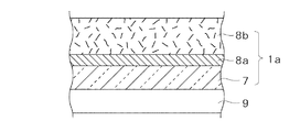
ここで、シールドフィルム1を所望の形状に切断する方法について説明する。
具体的に、図2に示すように、所望の形状に切断される前のシールドフィルムの積層構造を有した積層体1aが、保護部材9に積層される。尚、積層体1aは、絶縁層7側の面が保護部材9に当接するように積層されるがこれに限定されず、接着剤層8b側の面が保護部材9に当接するように積層されてもよい。
尚、保護部材9の積層において、離型剤(剥離剤)が用いられてもよい。
Here, a method for cutting the
Specifically, as shown in FIG. 2, a
In the lamination of the
そして、図3に示すように、カッタ11を用いて、接着剤層8b側から保護部材9を残して積層体1aを切断するハーフカットを行う。即ち、接着剤層8b側から保護部材9の途中までカッタ11で切断する。これにより、保護部材9上において、シールドフィルム1と剥離部1bとに切断され、剥離部1bが剥離可能にされる。
Then, as shown in FIG. 3, the
そして、図4に示すように、剥離部1bが剥離され、所望の形状に切断されたシールドフィルム1が保護部材9に積層された状態となる。また、図4に示すように、複数のシールドフィルム1を保護部材9上に積層することが可能になっている。
And as shown in FIG. 4, the peeling
尚、シールドフィルム1を所望の形状に切断する工程はこれに限定されない。例えば、図5に示すように、積層体1aの絶縁層7側の面をシート状のゴム、樹脂等の保護シート12に当接するように、当該シート12に不動に載置して積層体1aをカッタ11で所望の形状に切断して、シールドフィルム1を得てもよい。
In addition, the process of cutting the
(シールドフィルム載置工程、加熱プレス工程)
そして、図6に示すように、シールドフィルム1が積層された保護部材9(図4参照)から、シールドフィルム1を剥離してプリント基板5の所望の位置に載置すると共に、シールドフィルム1とプリント基板5とを加熱プレスすることで、図7に示すようなシールドプリント配線板10が製造される。尚、シールドフィルム1は、絶縁層7が露出された状態で加熱プレスされるため、絶縁層7は耐熱性樹脂で形成されることが好ましい。
(Shield film placement process, heating press process)
Then, as shown in FIG. 6, the
このように、絶縁層は樹脂硬化度が90%以上になるまで重合が進行した樹脂で形成されている。従って、絶縁層は、従来の保護層の機能を備えるため、プリント配線板との加熱プレス前において、シールドフィルム1は絶縁層を保護する保護層をない状態にすることができる。また、加熱プレス時においても絶縁層を保護する必要がないため、保護層を積層せずに加熱プレス工程を行うことができる。その結果、加熱プレス工程後において、シールドプリント配線板のシールドフィルムから保護層を剥離する工程を不要とすることができ、コストを削減することができる。
In this way, the insulating layer is formed of a resin that has been polymerized until the degree of cure of the resin reaches 90% or more. Therefore, since the insulating layer has the function of a conventional protective layer, the
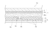
(シールドプリント配線板10の構成)
シールドプリント配線板10は、配線パターン3(グランド用配線パターン3b及び信号用配線パターン3a)が形成されたベース部材2と、ベース部材2上に積層されると共にグランド用配線パターン3bの少なくとも一部(非絶縁部3c)が絶縁除去部4aにより露出された絶縁フィルム4と、を有するプリント基板5にシールドフィルム1を貼り貼りあわせ加熱プレスされて形成される。
シールドフィルム1はプリント基板5との貼りあわせ面に導電性を有した接着剤層8bを有しているため、加熱プレス時に絶縁フィルム4のグランド用配線パターン3bが露出される箇所に埋め込まれる。これにより、グランド用配線パターン3bの非絶縁部3cとシールド層としての金属層8aとが電気的に接続され、シールドフィルム電磁波シールド機能がより向上されるようになっている。
(Configuration of shield printed wiring board 10)
The shield printed
Since the
また、シールドフィルム1は、一般的に絶縁層、シールド層、及び、接着剤層を合わせた層厚よりも厚い保護層を有していないため、従来よりも半分以上薄く形成されていることになる。従って、加熱プレス時において、シールドフィルム1は、プリント基板5の凹凸および絶縁除去部4aに追従しやすいものとなる。即ち、シールドプリント配線板10において、シールドフィルム1の接着剤層8bはプリント基板5の凹凸に沿って追従するとともに、絶縁除去部4aにも追従するため、絶縁除去部4aと接着剤層8bと接着面に空隙が発生するのを防止することができる。従って、上記のシールドフィルム1を用いることにより、シールドプリント配線板10におけるプリント基板5への接着剤層8bの埋め込み性を向上することができる。
Moreover, since the
1 シールドフィルム
1a 積層体
1b 剥離部
2 ベース部材
3 配線パターン
3a 信号用配線パターン
3b グランド用配線パターン
3c 非絶縁部
4 絶縁フィルム
4a 絶縁除去部
5 プリント基板
7 絶縁層
8a 金属層
8b 接着剤層
9 保護部材
10 シールドプリント配線板
11 カッタ
DESCRIPTION OF
Claims (4)
前記シールドフィルムをプリント基板に載置する工程と、
前記シールドフィルムと前記プリント基板とを加熱プレスする工程と
を備え、
前記シールドフィルムを形成する工程は、
前記絶縁層側の面が保護部材に当接するように当該保護部材に積層された前記シールドフィルムを、前記接着剤層側から前記保護部材を残して前記積層体を切断するハーフカット工程と、
切断された前記シールドフィルムを前記保護部材から剥離する工程と
を備えたことを特徴とするシールドプリント配線板の製造方法。 Forming a shield film having an insulating layer which is a resin whose polymerization has progressed to a degree of resin curing of 90% or more, a shield layer laminated on the insulating layer, and an adhesive layer laminated on the shield layer; Process,
Placing the shield film on a printed circuit board;
A step of heating and pressing the shield film and the printed circuit board;
The step of forming the shield film includes:
A half-cut step of cutting the laminate, leaving the protective member from the adhesive layer side, the shield film laminated on the protective member so that the surface on the insulating layer side is in contact with the protective member;
And a step of peeling the cut shield film from the protective member. A method for producing a shield printed wiring board, comprising:
前記シールドフィルムをプリント基板に載置する工程と、
前記シールドフィルムと前記プリント基板とを加熱プレスする工程と
を備え、
前記シールドフィルムを形成する工程は、
前記シールドフィルムを、前記絶縁層側の面が保護シートに当接するように当該保護シートに載置して当該積層体を切断するカット工程を備えたことを特徴とするシールドプリント配線板の製造方法。 Forming a shield film having an insulating layer which is a resin whose polymerization has progressed to a degree of resin curing of 90% or more, a shield layer laminated on the insulating layer, and an adhesive layer laminated on the shield layer; Process,
Placing the shield film on a printed circuit board;
A step of heating and pressing the shield film and the printed circuit board;
The step of forming the shield film includes:
A method for producing a shielded printed wiring board, comprising: a cutting step of placing the shield film on the protective sheet so that the surface on the insulating layer side is in contact with the protective sheet and cutting the laminate. .
前記シールドフィルムをプリント基板に載置する工程と、
前記シールドフィルムと前記プリント基板とを加熱プレスする工程と
を備え、
前記シールドフィルムを形成する工程は、
前記絶縁層側の面が保護部材に当接するように当該保護部材に積層された前記シールドフィルムを、前記接着剤層側から前記保護部材を残して前記積層体を切断するハーフカット工程と、
切断された前記シールドフィルムを前記保護部材から剥離する工程と
を備えたことを特徴とするシールドプリント配線板の製造方法。 Forming a shield film having an insulating layer, which is a resin that has been polymerized until the resin curing degree is 90% or more, and an isotropic conductive adhesive layer laminated on the insulating layer;
Placing the shield film on a printed circuit board;
A step of heating and pressing the shield film and the printed circuit board;
The step of forming the shield film includes:
A half-cut step of cutting the laminate, leaving the protective member from the adhesive layer side, the shield film laminated on the protective member so that the surface on the insulating layer side is in contact with the protective member;
And a step of peeling the cut shield film from the protective member. A method for producing a shield printed wiring board, comprising:
前記シールドフィルムをプリント基板に載置する工程と、
前記シールドフィルムと前記プリント基板とを加熱プレスする工程と
を備え、
前記シールドフィルムを形成する工程は、
前記シールドフィルムを、前記絶縁層側の面が保護シートに当接するように当該保護シートに載置して当該積層体を切断するカット工程を備えたことを特徴とするシールドプリント配線板の製造方法。 Forming a shield film having an insulating layer, which is a resin that has been polymerized until the resin curing degree is 90% or more, and an isotropic conductive adhesive layer laminated on the insulating layer;
Placing the shield film on a printed circuit board;
A step of heating and pressing the shield film and the printed circuit board;
The step of forming the shield film includes:
A method for producing a shielded printed wiring board, comprising: a cutting step of placing the shield film on the protective sheet so that the surface on the insulating layer side is in contact with the protective sheet and cutting the laminate. .
Priority Applications (1)
| Application Number | Priority Date | Filing Date | Title |
|---|---|---|---|
| JP2015235803A JP2016029748A (en) | 2015-12-02 | 2015-12-02 | Method for manufacturing shield printed wiring board |
Applications Claiming Priority (1)
| Application Number | Priority Date | Filing Date | Title |
|---|---|---|---|
| JP2015235803A JP2016029748A (en) | 2015-12-02 | 2015-12-02 | Method for manufacturing shield printed wiring board |
Related Parent Applications (1)
| Application Number | Title | Priority Date | Filing Date |
|---|---|---|---|
| JP2012278551A Division JP2014123630A (en) | 2012-12-20 | 2012-12-20 | Method for manufacturing shielding printed wiring board, shielding film, and shielding printed wiring board |
Publications (2)
| Publication Number | Publication Date |
|---|---|
| JP2016029748A true JP2016029748A (en) | 2016-03-03 |
| JP2016029748A5 JP2016029748A5 (en) | 2016-11-10 |
Family
ID=55435491
Family Applications (1)
| Application Number | Title | Priority Date | Filing Date |
|---|---|---|---|
| JP2015235803A Pending JP2016029748A (en) | 2015-12-02 | 2015-12-02 | Method for manufacturing shield printed wiring board |
Country Status (1)
| Country | Link |
|---|---|
| JP (1) | JP2016029748A (en) |
Cited By (4)
| Publication number | Priority date | Publication date | Assignee | Title |
|---|---|---|---|---|
| WO2018147423A1 (en) * | 2017-02-13 | 2018-08-16 | タツタ電線株式会社 | Ground member, shielded printed circuit board, and method for manufacturing shielded printed circuit board |
| WO2018147426A1 (en) * | 2017-02-13 | 2018-08-16 | タツタ電線株式会社 | Shield film, shielded printed circuit board, and method for manufacturing shielded printed circuit board |
| JP2018129472A (en) * | 2017-02-10 | 2018-08-16 | 信越ポリマー株式会社 | Electromagnetic wave shielding film and printed wiring board with electromagnetic wave shielding film |
| WO2018147429A1 (en) * | 2017-02-13 | 2018-08-16 | タツタ電線株式会社 | Ground member, shielded printed circuit board, and method for manufacturing shielded printed circuit board |
Citations (4)
| Publication number | Priority date | Publication date | Assignee | Title |
|---|---|---|---|---|
| JPH08125380A (en) * | 1994-10-19 | 1996-05-17 | Sumitomo Electric Ind Ltd | Shielded flexible wiring-board and manufacturing method thereof |
| JP2005056906A (en) * | 2003-08-05 | 2005-03-03 | Reiko Co Ltd | Electromagnetic wave shielding transfer film |
| JP2007294918A (en) * | 2006-03-29 | 2007-11-08 | Tatsuta System Electronics Kk | Shielding film and shielding printed wiring board |
| JP2011171523A (en) * | 2010-02-19 | 2011-09-01 | Toyo Ink Sc Holdings Co Ltd | Curable electromagnetic shielding adhesive film and method for producing the same |
-
2015
- 2015-12-02 JP JP2015235803A patent/JP2016029748A/en active Pending
Patent Citations (4)
| Publication number | Priority date | Publication date | Assignee | Title |
|---|---|---|---|---|
| JPH08125380A (en) * | 1994-10-19 | 1996-05-17 | Sumitomo Electric Ind Ltd | Shielded flexible wiring-board and manufacturing method thereof |
| JP2005056906A (en) * | 2003-08-05 | 2005-03-03 | Reiko Co Ltd | Electromagnetic wave shielding transfer film |
| JP2007294918A (en) * | 2006-03-29 | 2007-11-08 | Tatsuta System Electronics Kk | Shielding film and shielding printed wiring board |
| JP2011171523A (en) * | 2010-02-19 | 2011-09-01 | Toyo Ink Sc Holdings Co Ltd | Curable electromagnetic shielding adhesive film and method for producing the same |
Cited By (9)
| Publication number | Priority date | Publication date | Assignee | Title |
|---|---|---|---|---|
| JP2018129472A (en) * | 2017-02-10 | 2018-08-16 | 信越ポリマー株式会社 | Electromagnetic wave shielding film and printed wiring board with electromagnetic wave shielding film |
| JP7228330B2 (en) | 2017-02-10 | 2023-02-24 | 信越ポリマー株式会社 | Electromagnetic wave shielding film and printed wiring board with electromagnetic wave shielding film |
| WO2018147423A1 (en) * | 2017-02-13 | 2018-08-16 | タツタ電線株式会社 | Ground member, shielded printed circuit board, and method for manufacturing shielded printed circuit board |
| WO2018147426A1 (en) * | 2017-02-13 | 2018-08-16 | タツタ電線株式会社 | Shield film, shielded printed circuit board, and method for manufacturing shielded printed circuit board |
| WO2018147429A1 (en) * | 2017-02-13 | 2018-08-16 | タツタ電線株式会社 | Ground member, shielded printed circuit board, and method for manufacturing shielded printed circuit board |
| JPWO2018147423A1 (en) * | 2017-02-13 | 2019-11-21 | タツタ電線株式会社 | Ground member, shield printed wiring board, and method for manufacturing shield printed wiring board |
| US10638598B2 (en) | 2017-02-13 | 2020-04-28 | Tatsuta Electric Wire & Cable Co., Ltd. | Ground member, shielded printed circuit board, and method for manufacturing shielded printed circuit board |
| JP2020096189A (en) * | 2017-02-13 | 2020-06-18 | タツタ電線株式会社 | Ground member, shield printed wiring board, and method of manufacturing shield printed wiring board |
| TWI715825B (en) * | 2017-02-13 | 2021-01-11 | 日商拓自達電線股份有限公司 | Grounding member, shielding printed wiring board and manufacturing method of shielding printed wiring board |
Similar Documents
| Publication | Publication Date | Title |
|---|---|---|
| WO2014097933A1 (en) | Method for manufacturing shield printed circuit board, and shield film and shield printed circuit board | |
| KR20160013048A (en) | Electromagnetic wave shielding film, printed wire board using same, and rolled copper foil | |
| JP4360774B2 (en) | Reinforcing shield film and shield flexible printed wiring board | |
| JP6187568B2 (en) | Laminated body for electromagnetic wave shield, electromagnetic wave shield laminated body, electronic device and manufacturing method thereof | |
| JP2016029748A (en) | Method for manufacturing shield printed wiring board | |
| JP7256618B2 (en) | Electromagnetic wave shielding film with transfer film, method for producing electromagnetic wave shielding film with transfer film, and method for producing shield printed wiring board | |
| JP2014112576A (en) | Shield film | |
| JP2017191955A (en) | Laminate for shielding electromagnetic waves, electromagnetic wave shield laminate, electronic device and method for manufacturing the same | |
| US9820376B2 (en) | Shape-retaining film, and shape-retaining-type flexible circuit board provided with same shape-retaining film | |
| JP7023836B2 (en) | Electromagnetic wave shield film | |
| JP2019065069A (en) | Conductive adhesive sheet | |
| JP4324029B2 (en) | Laminated film having metal film and adhesive layer and method for producing the same | |
| TWI754611B (en) | Conductive bonding sheet for fpc and fpc using the same | |
| WO2020090726A1 (en) | Electromagnetic shielding film, method for producing shielded printed wiring board, and shielded printed wiring board | |
| JP2023072062A (en) | Shielded printed wiring board | |
| KR101411978B1 (en) | The fabrication method of adhesive tape for thin electromagnetic shield with color layer in polymer film and adhesive tape thereby | |
| TWI728082B (en) | Conductive reinforcing member, flexible printed wiring board, and manufacturing method of flexible printed wiring board | |
| TWI829973B (en) | Electromagnetic wave shielding film | |
| TWI834572B (en) | Manufacturing method of shielded printed wiring board and shielded printed wiring board | |
| JP7404927B2 (en) | magnetic sheet | |
| JP2019161101A (en) | Electromagnetic wave shield film and shield printed wiring board | |
| JP6731393B2 (en) | Electromagnetic wave shielding film | |
| TWI725334B (en) | Connection film, manufacturing method of shielding printed wiring board, and shielding printed wiring board | |
| JP2021082658A (en) | Electromagnetic wave-shield film, electromagnetic wave-shield film-attached print wiring board, and manufacturing method thereof | |
| JP6286273B2 (en) | Shield film, shield printed wiring board, and method for manufacturing shield printed wiring board |
Legal Events
| Date | Code | Title | Description |
|---|---|---|---|
| A621 | Written request for application examination |
Free format text: JAPANESE INTERMEDIATE CODE: A621 Effective date: 20151202 |
|
| A521 | Request for written amendment filed |
Free format text: JAPANESE INTERMEDIATE CODE: A523 Effective date: 20160920 |
|
| A977 | Report on retrieval |
Free format text: JAPANESE INTERMEDIATE CODE: A971007 Effective date: 20161017 |
|
| A131 | Notification of reasons for refusal |
Free format text: JAPANESE INTERMEDIATE CODE: A131 Effective date: 20161122 |
|
| A02 | Decision of refusal |
Free format text: JAPANESE INTERMEDIATE CODE: A02 Effective date: 20170606 |