JP2016004635A - Lamp device and lighting device - Google Patents

Lamp device and lighting device Download PDF

Info

Publication number
JP2016004635A
JP2016004635A JP2014122884A JP2014122884A JP2016004635A JP 2016004635 A JP2016004635 A JP 2016004635A JP 2014122884 A JP2014122884 A JP 2014122884A JP 2014122884 A JP2014122884 A JP 2014122884A JP 2016004635 A JP2016004635 A JP 2016004635A
Authority
JP
Japan
Prior art keywords
substrate
housing
lamp device
light emitting
diffusion plate
Prior art date
Legal status (The legal status is an assumption and is not a legal conclusion. Google has not performed a legal analysis and makes no representation as to the accuracy of the status listed.)
Abandoned
Application number
JP2014122884A
Other languages
Japanese (ja)
Inventor
淳一 木宮
Junichi Kimiya
淳一 木宮
筏 邦彦
Kunihiko Ikada
邦彦 筏
善之 玉木
Yoshiyuki Tamaki
善之 玉木
大塚 誠
Makoto Otsuka
誠 大塚
Current Assignee (The listed assignees may be inaccurate. Google has not performed a legal analysis and makes no representation or warranty as to the accuracy of the list.)
Toshiba Lighting and Technology Corp
Original Assignee
Toshiba Lighting and Technology Corp
Priority date (The priority date is an assumption and is not a legal conclusion. Google has not performed a legal analysis and makes no representation as to the accuracy of the date listed.)
Filing date
Publication date
Application filed by Toshiba Lighting and Technology Corp filed Critical Toshiba Lighting and Technology Corp
Priority to JP2014122884A priority Critical patent/JP2016004635A/en
Priority to CN201520062633.5U priority patent/CN204459933U/en
Publication of JP2016004635A publication Critical patent/JP2016004635A/en
Abandoned legal-status Critical Current

Links

Images

Landscapes

  • Arrangement Of Elements, Cooling, Sealing, Or The Like Of Lighting Devices (AREA)
  • Non-Portable Lighting Devices Or Systems Thereof (AREA)
  • Fastening Of Light Sources Or Lamp Holders (AREA)

Abstract

PROBLEM TO BE SOLVED: To provide a lamp device which enables weight reduction while securing heat radiation performance and achieves good manufacturability, and to provide a lighting device.SOLUTION: A lamp device 10 includes: a light emitting module 12; a housing 11; and a mouth piece 14. The light emitting module 12 includes a substrate 50 and a light emitting element 51 mounted on the substrate 50. The housing 11 includes a substrate attachment part 20, to which the substrate 50 is attached, at one end side. The substrate attachment part 20 is formed by insert molding in which a heat diffusion plate 28 is covered with a resin part 29. A substrate attachment surface 22 exposed from the resin part 29 and to which the substrate 50 is attached is formed on the heat diffusion plate 28. The mouth piece 14 is provided at the other end side of the housing 11.

Description

本発明の実施形態は、発光素子を用いたランプ装置、およびこのランプ装置を用いた照明装置に関する。   Embodiments described herein relate generally to a lamp device using a light emitting element and an illumination device using the lamp device.

従来、発光素子を用いたランプ装置として、例えばGX53形の口金を用いたフラット形のランプ装置や、E形の口金を用いた電球形のランプ装置等がある。   Conventionally, as a lamp device using a light emitting element, for example, there are a flat lamp device using a GX53 type base, a light bulb type lamp device using an E type base, and the like.

このようなランプ装置では、アルミダイカスト等の金属製の筐体を使用し、筐体の一端側に発光素子を有する発光モジュールを配置し、筐体の他端側に口金を配置している。そして、発光素子が点灯時に発生する熱を筐体に伝達し、筐体から外気中に放熱する放熱構成が採られている。また、筐体からの放熱性を向上させるために、筐体の外面に放熱フィンを設けたものもある。   In such a lamp device, a metal housing such as aluminum die casting is used, a light emitting module having a light emitting element is disposed on one end side of the housing, and a base is disposed on the other end side of the housing. And the heat dissipation structure which transmits the heat | fever which generate | occur | produces at the time of a light emitting element lighting to a housing | casing and radiates heat | fever from the housing | casing in the open air is taken. In addition, in order to improve the heat dissipation from the housing, there are some which have heat radiation fins on the outer surface of the housing.

特開2012−22994号公報JP 2012-22994 A

ランプ装置は、放熱性を考慮して金属製の筐体を用いているため、重くなってしまう問題がある。また、ランプ装置の外面に金属面が露出するため、筐体の表面加工や塗装が必要となってしまう問題がある。   Since the lamp device uses a metal casing in consideration of heat dissipation, there is a problem that the lamp device becomes heavy. In addition, since the metal surface is exposed on the outer surface of the lamp device, there is a problem that surface processing or painting of the housing is required.

本発明が解決しようとする課題は、放熱性を確保しながら軽量化できるとともに製造性がよいランプ装置、および照明装置を提供することである。   The problem to be solved by the present invention is to provide a lamp device and an illuminating device that can be reduced in weight while ensuring heat dissipation and have good manufacturability.

実施形態のランプ装置は、発光モジュール、筐体および口金を備える。発光モジュールは、基板および基板に実装された発光素子を有する。筐体は、一端側に基板を取り付ける基板取付部を有する。基板取付部は、熱拡散板を樹脂部で覆うインサート成形によって形成しており、熱拡散板に樹脂部から露出して基板が取り付けられる基板取付面を形成する。口金は、筐体の他端側に設ける。   The lamp device of the embodiment includes a light emitting module, a housing, and a base. The light emitting module includes a substrate and a light emitting element mounted on the substrate. The housing has a substrate attachment portion for attaching the substrate to one end side. The board attachment portion is formed by insert molding that covers the heat diffusion plate with the resin portion, and forms a substrate attachment surface on which the substrate is attached to the heat diffusion plate exposed from the resin portion. The base is provided on the other end side of the housing.

本発明によれば、放熱性を確保しながら軽量化できるとともに製造性をよくすることが期待できる。   According to the present invention, it can be expected that the weight can be reduced while the heat dissipation is ensured and the productivity is improved.

第1の実施形態を示すランプ装置の断面図である。It is sectional drawing of the lamp device which shows 1st Embodiment. 同上ランプ装置の分解状態の斜視図である。It is a perspective view of the decomposition | disassembly state of a lamp device same as the above. 同上ランプ装置の筐体および発光モジュールの底面図である。It is a bottom view of the housing | casing of a lamp device same as the above and a light emitting module. 同上ランプ装置を用いた照明装置の斜視図である。It is a perspective view of the illuminating device using a lamp device same as the above. 第2の実施形態を示すランプ装置の断面図である。It is sectional drawing of the lamp device which shows 2nd Embodiment. 第3の実施形態を示すランプ装置の断面図である。It is sectional drawing of the lamp device which shows 3rd Embodiment.

以下、第1の実施形態を、図1ないし図4を参照して説明する。   Hereinafter, a first embodiment will be described with reference to FIGS. 1 to 4.

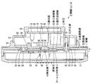
図1および図2に、フラット形の形態のランプ装置10を示す。なお、以下、ランプ装置10の一端側を前(前側や前面)、他端側を後(後側や後面)として説明する。   1 and 2 show a flat lamp device 10. In the following description, one end side of the lamp device 10 is assumed to be the front (front side or front side) and the other end side is assumed to be the rear side (rear side or rear side).

ランプ装置10は、筐体11、この筐体11の前側に取り付けられた発光モジュール12およびグローブ13、筐体11の後側に取り付けられた口金14、および口金14内に収容された点灯回路15を備えている。   The lamp device 10 includes a housing 11, a light emitting module 12 and a globe 13 attached to the front side of the housing 11, a base 14 attached to the rear side of the housing 11, and a lighting circuit 15 accommodated in the base 14. It has.

まず、図1ないし図3に示すように、筐体11は、基板取付部20、およびこの基板取付部20の外周部に形成される外周部21を備えている。基板取付部20は、平板状に形成されている。外周部21は、円筒状に形成され、基板取付部20の前側に突出されている。   First, as shown in FIGS. 1 to 3, the housing 11 includes a board mounting portion 20 and an outer peripheral portion 21 formed on the outer peripheral portion of the board mounting portion 20. The board mounting portion 20 is formed in a flat plate shape. The outer peripheral portion 21 is formed in a cylindrical shape and protrudes to the front side of the substrate mounting portion 20.

基板取付部20の前面中央には、発光モジュール12が取り付けられる基板取付面22が形成されている。基板取付面22の周囲位置には、複数の取付孔23が基板取付部20を貫通して形成されているとともに、1つの配線孔24が基板取付部20を貫通して形成されている。基板取付部20の後面には口金14が嵌り込む円筒状の壁部25が突設されている。   A substrate attachment surface 22 to which the light emitting module 12 is attached is formed at the front center of the substrate attachment portion 20. A plurality of attachment holes 23 are formed through the substrate attachment portion 20 at positions around the substrate attachment surface 22, and one wiring hole 24 is formed through the substrate attachment portion 20. A cylindrical wall portion 25 into which the base 14 is fitted projects from the rear surface of the substrate mounting portion 20.

外周部21の内周面には、グローブ13を取り付けるための複数の係止部26が突設されている。   On the inner peripheral surface of the outer peripheral portion 21, a plurality of locking portions 26 for attaching the globe 13 are projected.

そして、筐体11は、熱拡散板28を樹脂部29で覆うインサート成形によって一体に形成されている。   The casing 11 is integrally formed by insert molding that covers the heat diffusing plate 28 with the resin portion 29.

熱拡散板28は、熱を拡散させる作用が良好な例えば金属材料によって形成されている。金属材料としては例えばアルミニウムが用いられる。本実施形態では、熱拡散板28は円板状に形成され、基板取付部20に配置されている。   The heat diffusing plate 28 is made of, for example, a metal material that has a good effect of diffusing heat. For example, aluminum is used as the metal material. In the present embodiment, the heat diffusing plate 28 is formed in a disc shape and is disposed on the substrate mounting portion 20.

熱拡散板28の中央には、熱拡散板28の前側に突出して樹脂部29の前側に露出する突部30が形成され、この突部30の前面に基板取付面22が形成されている。基板取付面22は、四角形状に形成されている。さらに、基板取付面22は、平面状に形成され、基板取付面22の周囲の樹脂部29の前面と面一かあるいはその樹脂部29の前面よりもわずか突出されている。   At the center of the heat diffusing plate 28, a protrusion 30 protruding to the front side of the heat diffusing plate 28 and exposed to the front side of the resin portion 29 is formed, and a substrate mounting surface 22 is formed on the front surface of the protrusion 30. The board mounting surface 22 is formed in a square shape. Further, the substrate mounting surface 22 is formed in a flat shape and is flush with the front surface of the resin portion 29 around the substrate mounting surface 22 or slightly protrudes from the front surface of the resin portion 29.

各取付孔23の位置には、熱拡散板28に貫通孔31が形成されているとともに、貫通孔31(取付孔23)の内側を覆って樹脂部29が円筒状に形成されている。各取付孔23の内側に形成される樹脂部29は、熱拡散板28を絶縁するとともに、熱拡散板28の前面の樹脂部29と熱拡散板28の後面の樹脂部29とを結合する結合部32としても機能している。   Through holes 31 are formed in the heat diffusing plate 28 at positions of the respective mounting holes 23, and a resin portion 29 is formed in a cylindrical shape so as to cover the inside of the through holes 31 (mounting holes 23). The resin portion 29 formed inside each mounting hole 23 insulates the heat diffusion plate 28 and bonds the resin portion 29 on the front surface of the heat diffusion plate 28 and the resin portion 29 on the rear surface of the heat diffusion plate 28. It also functions as part 32.

配線孔24の位置には、熱拡散板28に貫通孔33が形成されているとともに、貫通孔33(配線孔24)の内側を覆って樹脂部29が円筒状に形成されている。貫通孔33の内側に形成される樹脂部29は、熱拡散板28を絶縁するとともに、熱拡散板28の前面の樹脂部29と熱拡散板28の後面の樹脂部29とを結合する結合部34としても機能している。   A through hole 33 is formed in the heat diffusion plate 28 at the position of the wiring hole 24, and a resin portion 29 is formed in a cylindrical shape so as to cover the inside of the through hole 33 (wiring hole 24). The resin part 29 formed inside the through hole 33 insulates the heat diffusion plate 28 and joins the resin part 29 on the front surface of the heat diffusion plate 28 and the resin part 29 on the rear surface of the heat diffusion plate 28. It also functions as 34.

基板取付面22の内側位置には、熱拡散板28に貫通孔35が形成されているとともに、貫通孔35の周囲で突部30の前面に段部36が形成されている。貫通孔33および段部36には、熱拡散板28の後面の樹脂部29から連続して樹脂部29が充填されている。   A through hole 35 is formed in the heat diffusion plate 28 at a position inside the substrate mounting surface 22, and a step portion 36 is formed on the front surface of the protrusion 30 around the through hole 35. The through hole 33 and the stepped portion 36 are filled with the resin portion 29 continuously from the resin portion 29 on the rear surface of the heat diffusion plate 28.

筐体11をインサート成形する際、金型内に熱拡散板28を配置し、金型内に溶融樹脂を充填して樹脂部29を形成するが、金型内に溶融樹脂を充填するゲートとして熱拡散板28の貫通孔35を用いる。貫通孔35は基板取付部20の中央に位置するため、金型内に注入した溶融樹脂が基板取付部20の外径方向および外周部21に向けて均等に広がり、樹脂部29の形成領域全体に溶融樹脂を充填することができる。   When the housing 11 is insert-molded, the heat diffusion plate 28 is disposed in the mold, and the resin portion 29 is formed by filling the mold with a molten resin, but as a gate for filling the mold with the molten resin. The through hole 35 of the heat diffusing plate 28 is used. Since the through-hole 35 is located at the center of the substrate mounting portion 20, the molten resin injected into the mold spreads evenly toward the outer diameter direction and the outer peripheral portion 21 of the substrate mounting portion 20, and the entire region where the resin portion 29 is formed Can be filled with molten resin.

貫通孔35の内側に充填された樹脂部29は、熱拡散板28(段部36)の前面の樹脂部29と熱拡散板28の後面の樹脂部29とを結合する結合部37として機能している。この結合部37の前面には、インサート成形に伴って生じる窪み部38が形成されている。なお、窪み部38は、基板取付面22に発光モジュール12を取り付ける際に密着性を高めるためのシリコーン等のグリスを介在させる場合に、そのグリスを入れておくことができる。   The resin portion 29 filled inside the through hole 35 functions as a coupling portion 37 that couples the resin portion 29 on the front surface of the heat diffusion plate 28 (step portion 36) and the resin portion 29 on the rear surface of the heat diffusion plate 28. ing. On the front surface of the connecting portion 37, a recessed portion 38 that is generated along with insert molding is formed. It should be noted that when the light emitting module 12 is attached to the substrate attachment surface 22, the recess 38 can be filled with grease such as silicone for enhancing adhesion.

樹脂部29は、絶縁性を有するとともに、例えば白色の高反射樹脂が用いられている。筐体11の基板取付部20の前面および外周部21の内周面には、樹脂部29によって高反射率の反射面39が形成されている。   The resin part 29 has an insulating property and, for example, a white highly reflective resin is used. On the front surface of the substrate mounting portion 20 of the housing 11 and the inner peripheral surface of the outer peripheral portion 21, a reflective surface 39 having a high reflectance is formed by the resin portion 29.

また、発光モジュール12は、基板50、およびこの基板50の前面に実装された発光素子51を備えている。さらに、基板50の前面には、発光素子51と点灯回路15とを接続するためのコネクタ52が実装されている。   The light emitting module 12 includes a substrate 50 and a light emitting element 51 mounted on the front surface of the substrate 50. Further, a connector 52 for connecting the light emitting element 51 and the lighting circuit 15 is mounted on the front surface of the substrate 50.

基板50は、例えば、熱伝導性に優れたアルミニウム等の金属あるいはセラミックス等で四角形板状に形成されている。基板50の大きさは、基板取付面22と同じ、基板取付面22よりも大きい、基板取付面22よりも小さい、のいずれかに形成されている。基板50の前面には、絶縁層を介して配線パターンが形成され、配線パターンに発光素子51およびコネクタ52が実装されている。さらに、配線パターン上には、発光素子51およびコネクタ52の実装部を除いて、反射率の高い白色の絶縁層が形成されている。そして、基板50は、基板50の後面を筐体11の基板取付面22に接合し、この基板50を通じて複数のねじ53を熱拡散板28の突部30に螺着することにより、熱拡散板28に熱的に接続されている。   The substrate 50 is formed in a square plate shape, for example, from a metal such as aluminum or ceramics having excellent thermal conductivity. The size of the substrate 50 is the same as that of the substrate attachment surface 22, is larger than the substrate attachment surface 22, or smaller than the substrate attachment surface 22. A wiring pattern is formed on the front surface of the substrate 50 via an insulating layer, and a light emitting element 51 and a connector 52 are mounted on the wiring pattern. Further, on the wiring pattern, a white insulating layer having a high reflectance is formed except for the mounting portion of the light emitting element 51 and the connector 52. Then, the substrate 50 is bonded to the substrate mounting surface 22 of the housing 11 at the rear surface of the substrate 50, and a plurality of screws 53 are screwed to the protrusions 30 of the heat diffusion plate 28 through the substrate 50. Thermally connected to 28.

発光素子51は、例えばLEDである。本実施形態では、発光素子51として、LEDチップが搭載された複数のSMD(Surface Mount Device)パッケージが用いられている。発光素子51は、白色系の照明光を放射する。なお、発光素子51は、COB(Chip On Board)モジュールでもよいし、EL素子等の他の発光素子を用いてもよい。   The light emitting element 51 is, for example, an LED. In the present embodiment, as the light emitting element 51, a plurality of SMD (Surface Mount Device) packages on which LED chips are mounted are used. The light emitting element 51 emits white illumination light. The light emitting element 51 may be a COB (Chip On Board) module or other light emitting element such as an EL element.

また、図1および図2に示すように、グローブ13は、透光性および拡散性を有する合成樹脂製で円板状に形成されている。グローブ13は、筐体11の下面を覆って、筐体11の外周部21の内側に嵌め込まれて取り付けられている。グローブ13には、外周部21の係止部26に引っ掛かって取り付けられる爪部56が形成されている。   Further, as shown in FIGS. 1 and 2, the globe 13 is made of a synthetic resin having translucency and diffusibility and is formed in a disc shape. The globe 13 is attached by being fitted inside the outer peripheral portion 21 of the housing 11 so as to cover the lower surface of the housing 11. The globe 13 is formed with a claw portion 56 that is hooked and attached to the locking portion 26 of the outer peripheral portion 21.

また、口金14は、例えばGX53形口金である。口金14は、口金本体60、およびこの口金本体60の後面から突出する一対のランプピン61(図4参照)を備えている。   The base 14 is, for example, a GX53 type base. The base 14 includes a base body 60 and a pair of lamp pins 61 (see FIG. 4) protruding from the rear surface of the base body 60.

口金本体60は、絶縁性を有する樹脂製で一体に形成されている。口金本体60は、環状部62、この環状部62の周縁部から前面側に突出する円筒状の嵌合部63、および環状部62の中央領域から後側に突出する円筒状の突出部64を有している。これにより、口金本体60は前面が開口され、口金本体60の内部に点灯回路15を収納する空間が形成されている。   The base body 60 is integrally formed of an insulating resin. The base body 60 includes an annular portion 62, a cylindrical fitting portion 63 protruding from the peripheral portion of the annular portion 62 to the front surface side, and a cylindrical protruding portion 64 protruding rearward from the central region of the annular portion 62. Have. Thus, the front surface of the base body 60 is opened, and a space for housing the lighting circuit 15 is formed inside the base body 60.

環状部62の前面には、複数のボス65が突設されている。そして、嵌合部63を筐体11の壁部25に嵌合し、複数のねじ66を筐体11の取付孔23を通じてボス65に螺着することにより、筐体11と口金14とが固定されている。   A plurality of bosses 65 project from the front surface of the annular portion 62. Then, the fitting portion 63 is fitted to the wall portion 25 of the housing 11, and a plurality of screws 66 are screwed to the boss 65 through the mounting holes 23 of the housing 11, whereby the housing 11 and the base 14 are fixed. Has been.

突出部64の外周面には、口金14の中心に対して対称位置であって一対のランプピン61を配置する位置からずれた位置に一対のL字形のキー溝67が形成されている。また、突出部64の端面68は平面状に形成されている。端面68の中央には、口金本体60を金型内で射出成型する際のゲートの位置に対応した窪み部69が形成されている。また、突出部64の内周面には、点灯回路15を保持する複数の保持部70が形成されている。   A pair of L-shaped key grooves 67 are formed on the outer peripheral surface of the projecting portion 64 at positions that are symmetrical with respect to the center of the base 14 and are displaced from the positions where the pair of lamp pins 61 are disposed. Further, the end surface 68 of the protrusion 64 is formed in a flat shape. In the center of the end face 68, a recess 69 corresponding to the position of the gate when the base body 60 is injection-molded in the mold is formed. A plurality of holding portions 70 that hold the lighting circuit 15 are formed on the inner peripheral surface of the protruding portion 64.

一対のランプピン61は、導電性を有する金属製で、先端には径大部71が形成されている。   The pair of lamp pins 61 is made of a conductive metal, and has a large-diameter portion 71 at the tip.

また、点灯回路15は、回路基板75、およびこの回路基板75に実装された複数の電子部品76を備えている。電子部品76のうち、リード線を有する大形の電子部品76は回路基板75の前面に実装され、チップ状の小形の電子部品76は回路基板75の後面に実装されている。   The lighting circuit 15 includes a circuit board 75 and a plurality of electronic components 76 mounted on the circuit board 75. Among the electronic components 76, a large electronic component 76 having a lead wire is mounted on the front surface of the circuit board 75, and a small chip-shaped electronic component 76 is mounted on the rear surface of the circuit board 75.

回路基板75は、口金14の突出部64の内側に挿入され、保持部70により口金14に保持されている。 The circuit board 75 is inserted inside the protrusion 64 of the base 14 and is held by the base 14 by the holding part 70.

点灯回路15の入力部と一対のランプピン61とが電線で電気的に接続されている。点灯回路15の出力部にはコネクタ付電線が接続され、このコネクタ付電線が筐体11の配線孔24を通じて発光モジュール12のコネクタ52に電気的に接続されている。そして、点灯回路15は、入力される交流電力を所定の直流電力に変換して発光モジュール12の発光素子51に供給する。   The input part of the lighting circuit 15 and the pair of lamp pins 61 are electrically connected by electric wires. An electric wire with a connector is connected to the output portion of the lighting circuit 15, and the electric wire with a connector is electrically connected to the connector 52 of the light emitting module 12 through the wiring hole 24 of the housing 11. The lighting circuit 15 converts the input AC power into predetermined DC power and supplies it to the light emitting element 51 of the light emitting module 12.

次に、図4に、ランプ装置10を用いる照明装置80を示す。照明装置80は、例えばダウンライトである。照明装置80は、器具本体81、ソケット82、およびランプ装置10を備える。   Next, FIG. 4 shows an illumination device 80 that uses the lamp device 10. The illumination device 80 is, for example, a downlight. The lighting device 80 includes an instrument body 81, a socket 82, and the lamp device 10.

器具本体81は、下方に開口され、反射体としても構成されている。   The instrument body 81 is opened downward and is also configured as a reflector.

ソケット82は、ソケット本体83、およびこのソケット本体83内に収容された端子を備えている。ソケット本体83は、絶縁性を有する樹脂製で環状に形成され、中央にはランプ装置10の突出部64が挿通される挿通孔84が形成されている。   The socket 82 includes a socket body 83 and terminals accommodated in the socket body 83. The socket body 83 is made of an insulating resin and is formed in an annular shape, and an insertion hole 84 through which the protruding portion 64 of the lamp device 10 is inserted is formed at the center.

ソケット本体83の下面には、ソケット82の中心に対して対称位置に、ランプ装置10の各ランプピン61を差し込んで回動する一対の接続孔85が形成されている。これら接続孔85は、ソケット本体83の周方向に沿って長い長孔で、その一端にはランプピン61の径大部71が挿通可能な孔部86が形成されている。各接続孔85の内側に、接続孔85に差し込まれたランプピン61が電気的に接続される端子が収容されている。   On the lower surface of the socket main body 83, a pair of connection holes 85 are formed at positions symmetrical with respect to the center of the socket 82 so that the lamp pins 61 of the lamp device 10 are inserted and rotated. These connection holes 85 are long holes extending along the circumferential direction of the socket body 83, and at one end thereof, a hole portion 86 through which the large diameter portion 71 of the lamp pin 61 can be inserted is formed. Inside each connection hole 85, a terminal to which the lamp pin 61 inserted into the connection hole 85 is electrically connected is accommodated.

ソケット本体83の内周面には、口金14のランプピン61を接続孔85に差し込んで回動するのに伴って、口金14の突出部64の外周面に形成されている略L字形のキー溝67に嵌り込んで口金14をソケット本体83に支持するキー87が突設されている。   A substantially L-shaped key groove formed on the outer peripheral surface of the projecting portion 64 of the base 14 as the lamp pin 61 of the base 14 is inserted into the connection hole 85 and rotated on the inner peripheral surface of the socket body 83. A key 87 that projects into the socket 67 and supports the base 14 to the socket body 83 is provided.

次に、本実施形態の作用について説明する。   Next, the operation of this embodiment will be described.

ランプ装置10をソケット82に装着するには、口金14の突出部64をソケット82の挿通孔84に挿入し、ランプ装置10の各ランプピン61をソケット82の接続孔85に差し込む。これに伴って、口金14の各キー溝67がソケット82の各キー87に嵌り込む。   In order to attach the lamp device 10 to the socket 82, the protrusion 64 of the base 14 is inserted into the insertion hole 84 of the socket 82, and each lamp pin 61 of the lamp device 10 is inserted into the connection hole 85 of the socket 82. Accordingly, each key groove 67 of the base 14 is fitted into each key 87 of the socket 82.

ランプ装置10をソケット82に押し付けた状態で、ランプ装置10を装着方向に回動させることにより、ランプ装置10の各ランプピン61がソケット82の接続孔85内を移動して接続孔85の内側に配置されている各端子に電気的に接続されるとともに、口金14のキー溝67がソケット82のキー87に嵌り込み、ランプ装置10がソケット82に支持される。   With the lamp device 10 pressed against the socket 82, the lamp device 61 is rotated in the mounting direction, so that each lamp pin 61 of the lamp device 10 moves in the connection hole 85 of the socket 82 and moves to the inside of the connection hole 85. The terminal is electrically connected to each terminal, and the key groove 67 of the base 14 is fitted into the key 87 of the socket 82, so that the lamp device 10 is supported by the socket 82.

また、ソケット82の端子およびランプ装置10のランプピン61を通じて点灯回路15に交流電力を供給することにより、点灯回路15が交流電力を所定の直流電力に変換して発光モジュール12の発光素子51に供給し、発光素子51が発光する。   Further, by supplying AC power to the lighting circuit 15 through the terminal of the socket 82 and the lamp pin 61 of the lamp device 10, the lighting circuit 15 converts the AC power into predetermined DC power and supplies it to the light emitting element 51 of the light emitting module 12. Then, the light emitting element 51 emits light.

発光素子51の光はグローブ13を透過して照明空間に照射される。   The light from the light emitting element 51 passes through the globe 13 and is irradiated to the illumination space.

発光素子51が発光時に発生する熱は、主に、基板50に熱伝導され、この基板50から筐体11の熱拡散板28に熱伝導される。熱拡散板28の中心部で基板50から熱伝導される熱を熱拡散板28の外径方向に拡散し、熱拡散板28の全域で熱拡散板28から樹脂部29に熱伝導する。これにより、樹脂部29に熱伝導された熱を樹脂部29の外面から外気中に放熱する。また、筐体11から口金14にも熱伝導され、口金14から外気中に放熱されるとともに口金14からソケット82に放熱される。   The heat generated when the light emitting element 51 emits light is mainly conducted to the substrate 50, and is conducted from the substrate 50 to the heat diffusion plate 28 of the housing 11. The heat conducted from the substrate 50 at the center of the heat diffusing plate 28 is diffused in the outer diameter direction of the heat diffusing plate 28, and is conducted from the heat diffusing plate 28 to the resin portion 29 throughout the heat diffusing plate 28. Thereby, the heat conducted to the resin part 29 is radiated from the outer surface of the resin part 29 into the outside air. Further, heat is conducted from the housing 11 to the base 14, and heat is radiated from the base 14 to the outside air and is radiated from the base 14 to the socket 82.

点灯回路15の電子部品76が発生する熱は、主に、口金14から外気中に放熱されるとともに口金14からソケット82に放熱される。   The heat generated by the electronic component 76 of the lighting circuit 15 is mainly dissipated from the base 14 into the outside air and from the base 14 to the socket 82.

そして、本実施形態のランプ装置10によれば、筐体11が熱拡散板28を樹脂部29で覆うインサート成形によって形成されるため、放熱性を確保しながら軽量化できるとともに、筐体全体を金属材料で形成する場合の表面加工や塗装の必要がなく、製造性をよくできる。さらに、筐体11の外表面が金属ではなく樹脂であるため、ランプ装置10の取り扱い時に筐体11が何かに当たっても損傷させるのを低減できる。   According to the lamp device 10 of the present embodiment, since the casing 11 is formed by insert molding that covers the heat diffusion plate 28 with the resin portion 29, the weight of the casing can be reduced while ensuring heat dissipation. There is no need for surface processing or painting when forming with a metal material, and the productivity can be improved. Furthermore, since the outer surface of the casing 11 is not a metal but a resin, it is possible to reduce damage even if the casing 11 hits something when the lamp device 10 is handled.

また、樹脂部29を白色の高反射樹脂で形成することにより、筐体11の基板取付部20の前面および外周部21の内周面に高反射率の反射面39を形成できるため、グローブ13の内側で乱反射する光を反射面39によって外部に効率よく反射させることができ、ランプ装置10の光取出効率を向上できる。   In addition, since the resin portion 29 is formed of a white highly reflective resin, a reflective surface 39 having a high reflectance can be formed on the front surface of the substrate mounting portion 20 of the housing 11 and the inner peripheral surface of the outer peripheral portion 21, so that the globe 13 The light diffusely reflected inside can be efficiently reflected to the outside by the reflecting surface 39, and the light extraction efficiency of the lamp device 10 can be improved.

また、基板取付部20には、基板取付面22の周囲位置に、熱拡散板28および樹脂部29を貫通して口金14を取り付ける複数の取付孔23が設けられているとともに、基板取付面22の内側位置に、熱拡散板28を貫通する樹脂部29の結合部37が設けられているため、ねじ止めで複数の取付孔23の周辺に負荷が加わっても、複数の取付孔23の間で樹脂部29が熱拡散板28から浮き上がるようなことがなく、熱拡散板28および樹脂部29との結合状態を維持できる。しかも、筐体11をインサート成形する際、金型内に熱拡散板28を配置し、金型内に溶融樹脂を充填して樹脂部29を形成するが、金型内に溶融樹脂を充填するゲートとして結合部37の部分を用いることにより、金型内に注入した溶融樹脂が樹脂部29の形成領域全体に均等に広がって、樹脂部29の形成領域全体に溶融樹脂を充填することができる。   In addition, the substrate mounting portion 20 is provided with a plurality of mounting holes 23 that pass through the heat diffusion plate 28 and the resin portion 29 and attach the base 14 around the substrate mounting surface 22, and the substrate mounting surface 22. Since the connecting portion 37 of the resin portion 29 penetrating the heat diffusion plate 28 is provided at the inner side of the mounting hole 23, even if a load is applied around the mounting holes 23 with screws, the space between the mounting holes 23 Thus, the resin portion 29 does not float from the heat diffusion plate 28, and the coupled state between the heat diffusion plate 28 and the resin portion 29 can be maintained. Moreover, when the housing 11 is insert-molded, the heat diffusion plate 28 is disposed in the mold, and the resin part 29 is formed by filling the mold with the molten resin, but the mold is filled with the molten resin. By using the portion of the coupling portion 37 as a gate, the molten resin injected into the mold can be spread evenly over the entire formation region of the resin portion 29, and the entire formation region of the resin portion 29 can be filled with the molten resin. .

また、筐体11は、熱拡散板28の基板取付面22のみが樹脂部から露出されているため、発光モジュール12の基板50が金属製でその金属面が基板取付面22に接しても、筐体11の外表面に電気が流れることがなく、特別な絶縁構造を用いなくても絶縁性を確保することができる。   Further, since only the substrate mounting surface 22 of the heat diffusing plate 28 is exposed from the resin portion of the housing 11, even if the substrate 50 of the light emitting module 12 is made of metal and the metal surface is in contact with the substrate mounting surface 22, Electricity does not flow on the outer surface of the housing 11, and insulation can be ensured without using a special insulating structure.

また、基板50の大きが基板取付面22よりも大きい場合には、熱拡散板28の金属面の露出が少なくなり、反射効果を高めることができる。   Further, when the size of the substrate 50 is larger than the substrate mounting surface 22, the exposure of the metal surface of the heat diffusing plate 28 is reduced and the reflection effect can be enhanced.

次に、図5に第2の実施形態を示す。なお、第1の実施形態と同じ構成については同じ符号を用い、その構成および作用効果についての説明は省略する。   Next, FIG. 5 shows a second embodiment. In addition, the same code | symbol is used about the same structure as 1st Embodiment, and the description about the structure and an effect is abbreviate | omitted.

筐体11の基板取付部20から外周部21に連続して熱拡散板28が形成されている。すなわち、熱拡散板28の周囲に、外周部21に配置される円筒状の縁部28aが形成されている。   A heat diffusion plate 28 is formed continuously from the substrate mounting portion 20 of the casing 11 to the outer peripheral portion 21. That is, a cylindrical edge portion 28 a disposed on the outer peripheral portion 21 is formed around the heat diffusion plate 28.

このように、熱拡散板28が筐体11の外周部21に配置される円筒状の縁部28aを有することで、筐体11の外周部21からの放熱効果を高めることができる。   As described above, the heat diffusing plate 28 has the cylindrical edge portion 28 a disposed on the outer peripheral portion 21 of the housing 11, so that the heat radiation effect from the outer peripheral portion 21 of the housing 11 can be enhanced.

次に、図6に第3の実施形態を示す。なお、第1の実施形態と同様の構成については同じ符号を用い、その構成および作用効果についての説明は省略する。   Next, FIG. 6 shows a third embodiment. In addition, the same code | symbol is used about the structure similar to 1st Embodiment, and the description about the structure and an effect is abbreviate | omitted.

図6に、電球形の形態のランプ装置10を示す。   FIG. 6 shows a lamp device 10 in the form of a light bulb.

ランプ装置10は、筐体11、筐体11の前側に取り付けられた発光モジュール12およびドーム状のグローブ13、筐体11の後側に取り付けられたカバー90および口金91、カバー90内に収容された点灯回路15を備えている。   The lamp device 10 is housed in a housing 11, a light emitting module 12 and a dome-shaped globe 13 attached to the front side of the housing 11, a cover 90 and a base 91 attached to the rear side of the housing 11, and the cover 90. The lighting circuit 15 is provided.

筐体11および発光モジュール12は、第1の実施形態と同様に構成されている。カバー90は、絶縁性を有する合成樹脂製で、前側が筐体11に取り付けられ、後側に口金91が取り付けられている。口金91は、E形口金である。   The casing 11 and the light emitting module 12 are configured in the same manner as in the first embodiment. The cover 90 is made of an insulating synthetic resin, and the front side is attached to the casing 11 and the base 91 is attached to the rear side. The base 91 is an E-shaped base.

この電球形の形態のランプ装置10においても、筐体11が熱拡散板28を樹脂部29で覆うインサート成形によって形成されるため、放熱性を確保しながら軽量化できるとともに、筐体全体を金属材料で形成する場合の表面加工や塗装の必要がなく、製造性をよくできる。   In this lamp-shaped lamp device 10 as well, since the casing 11 is formed by insert molding that covers the heat diffusion plate 28 with the resin portion 29, the weight can be reduced while ensuring heat dissipation, and the entire casing can be made of metal. There is no need for surface processing or painting when forming with a material, and the productivity can be improved.

本発明のいくつかの実施形態を説明したが、これらの実施形態は、例として提示したものであり、発明の範囲を限定することは意図していない。これら新規な実施形態は、その他の様々な形態で実施されることが可能であり、発明の要旨を逸脱しない範囲で、種々の省略、置き換え、変更を行うことができる。これら実施形態やその変形は、発明の範囲や要旨に含まれるとともに、特許請求の範囲に記載された発明とその均等の範囲に含まれる。   Although several embodiments of the present invention have been described, these embodiments are presented by way of example and are not intended to limit the scope of the invention. These novel embodiments can be implemented in various other forms, and various omissions, replacements, and changes can be made without departing from the scope of the invention. These embodiments and modifications thereof are included in the scope and gist of the invention, and are included in the invention described in the claims and the equivalents thereof.

10 ランプ装置
11 筐体
12 発光モジュール
14 口金
20 基板取付部
21 外周部
22 基板取付面
23 取付孔
28 熱拡散板
29 樹脂部
37 結合部
50 基板
51 発光素子
80 照明装置
82 ソケット
10 Lamp device
11 Enclosure
12 Light emitting module
14 base
20 Board mounting part
21 Outer part
22 Board mounting surface
23 Mounting hole
28 Heat diffusion plate
29 Resin section
37 Joint
50 substrates
51 Light emitting element
80 Lighting equipment
82 socket

Claims (5)

基板およびこの基板に実装された発光素子を有する発光モジュールと;
一端側に前記基板を取り付ける基板取付部を有し、この基板取付部は熱拡散板を樹脂部で覆うインサート成形によって形成されており、前記熱拡散板に前記樹脂部から露出して前記基板が取り付けられる基板取付面が形成されている筐体と;
前記筐体の他端側に設けられた口金と;
を具備することを特徴とするランプ装置。
A light emitting module having a substrate and a light emitting element mounted on the substrate;
A substrate mounting portion for mounting the substrate on one end side is formed by insert molding that covers the heat diffusion plate with a resin portion, and the substrate is exposed to the heat diffusion plate from the resin portion. A housing in which a substrate mounting surface to be mounted is formed;
A base provided on the other end of the housing;
A lamp device comprising:
前記筐体は、前記基板取付部の周囲に形成される外周部を有し、前記基板取付部から前記外周部に連続して前記熱拡散板および前記樹脂部が形成されている
ことを特徴とする請求項1記載のランプ装置。
The housing has an outer peripheral portion formed around the substrate mounting portion, and the heat diffusion plate and the resin portion are formed continuously from the substrate mounting portion to the outer peripheral portion. The lamp device according to claim 1.
前記基板取付部には、前記基板取付面の周囲位置に、前記熱拡散板および前記樹脂部を貫通して前記口金を取り付ける複数の取付孔が設けられているとともに、前記基板取付面の内側位置に、前記熱拡散板を貫通する前記樹脂部の結合部が設けられている
ことを特徴とする請求項1または2記載のランプ装置。
A plurality of attachment holes for attaching the base through the heat diffusion plate and the resin portion are provided in the substrate attachment portion at positions around the substrate attachment surface, and an inner position of the substrate attachment surface. 3. The lamp device according to claim 1, wherein a coupling portion of the resin portion penetrating the heat diffusion plate is provided.
前記筐体は、前記熱拡散板の前記基板取付面のみが前記樹脂部から露出されている
ことを特徴とする請求項1ないし3いずれか一記載のランプ装置。
4. The lamp device according to claim 1, wherein in the housing, only the substrate mounting surface of the heat diffusing plate is exposed from the resin portion. 5.
請求項1ないし4いずれか一記載のランプ装置と;
前記ランプ装置の前記口金を接続するソケットと;
を具備することを特徴とする照明装置。
A lamp device according to any one of claims 1 to 4;
A socket for connecting the base of the lamp device;
An illumination device comprising:
JP2014122884A 2014-06-13 2014-06-13 Lamp device and lighting device Abandoned JP2016004635A (en)

Priority Applications (2)

Application Number Priority Date Filing Date Title
JP2014122884A JP2016004635A (en) 2014-06-13 2014-06-13 Lamp device and lighting device
CN201520062633.5U CN204459933U (en) 2014-06-13 2015-01-29 Lamp device and lighting device

Applications Claiming Priority (1)

Application Number Priority Date Filing Date Title
JP2014122884A JP2016004635A (en) 2014-06-13 2014-06-13 Lamp device and lighting device

Publications (1)

Publication Number Publication Date
JP2016004635A true JP2016004635A (en) 2016-01-12

Family

ID=52686072

Family Applications (1)

Application Number Title Priority Date Filing Date
JP2014122884A Abandoned JP2016004635A (en) 2014-06-13 2014-06-13 Lamp device and lighting device

Country Status (2)

Country Link
JP (1) JP2016004635A (en)
CN (1) CN204459933U (en)

Also Published As

Publication number Publication date
CN204459933U (en) 2015-07-08

Similar Documents

Publication Publication Date Title
JP5699753B2 (en) Lamp apparatus and lighting apparatus
JP5320609B2 (en) Lamp apparatus and lighting apparatus
CN101978209A (en) Light-emitting element lamps and lighting equipment
CN101900265A (en) Bulb-shaped lamp and lighting fixture
US8803409B1 (en) Lamp device, light-emitting device and luminaire
JP5757214B2 (en) LED lighting device
CN204829426U (en) Lamp device and lighting device
CN102418860A (en) Lamp device and lighting device
JP2015076281A (en) Lighting device
JP2015079644A (en) Lighting device
JP2011171160A (en) Led lamp device and led lighting system
JP5534215B2 (en) Lamp device and lighting device
JP5768966B2 (en) Lamp apparatus and lighting apparatus
CN104048197B (en) Illumination light source and lighting apparatus
CN204164729U (en) Lamp device and ligthing paraphernalia
JP2013008582A (en) Lamp device
JP5679111B2 (en) Lamp apparatus and lighting apparatus
CN204164996U (en) Lamp device and ligthing paraphernalia
JP2012216305A (en) Lamp device and lighting fixture
JP5534216B2 (en) Lamp device and lighting device
JP2016004635A (en) Lamp device and lighting device
JP5660410B2 (en) Lamp device and lighting device
JP2016066500A (en) Lamp device and lighting system
CN203718434U (en) Lamp
JP2016058364A (en) Lamp device and luminaire

Legal Events

Date Code Title Description
A621 Written request for application examination

Free format text: JAPANESE INTERMEDIATE CODE: A621

Effective date: 20170313

A762 Written abandonment of application

Free format text: JAPANESE INTERMEDIATE CODE: A762

Effective date: 20171003