JP2015536626A - Mobile communication base station antenna - Google Patents
Mobile communication base station antenna Download PDFInfo
- Publication number
- JP2015536626A JP2015536626A JP2015545366A JP2015545366A JP2015536626A JP 2015536626 A JP2015536626 A JP 2015536626A JP 2015545366 A JP2015545366 A JP 2015545366A JP 2015545366 A JP2015545366 A JP 2015545366A JP 2015536626 A JP2015536626 A JP 2015536626A
- Authority
- JP
- Japan
- Prior art keywords
- radiating element
- base station
- mobile communication
- communication base
- station antenna
- Prior art date
- Legal status (The legal status is an assumption and is not a legal conclusion. Google has not performed a legal analysis and makes no representation as to the accuracy of the status listed.)
- Withdrawn
Links
Images


Classifications
-
- H—ELECTRICITY
- H01—ELECTRIC ELEMENTS
- H01Q—ANTENNAS, i.e. RADIO AERIALS
- H01Q13/00—Waveguide horns or mouths; Slot antennas; Leaky-waveguide antennas; Equivalent structures causing radiation along the transmission path of a guided wave
- H01Q13/10—Resonant slot antennas
- H01Q13/106—Microstrip slot antennas
-
- H—ELECTRICITY
- H01—ELECTRIC ELEMENTS
- H01Q—ANTENNAS, i.e. RADIO AERIALS
- H01Q5/00—Arrangements for simultaneous operation of antennas on two or more different wavebands, e.g. dual-band or multi-band arrangements
-
- H—ELECTRICITY
- H01—ELECTRIC ELEMENTS
- H01Q—ANTENNAS, i.e. RADIO AERIALS
- H01Q1/00—Details of, or arrangements associated with, antennas
- H01Q1/12—Supports; Mounting means
- H01Q1/22—Supports; Mounting means by structural association with other equipment or articles
- H01Q1/24—Supports; Mounting means by structural association with other equipment or articles with receiving set
- H01Q1/241—Supports; Mounting means by structural association with other equipment or articles with receiving set used in mobile communications, e.g. GSM
- H01Q1/246—Supports; Mounting means by structural association with other equipment or articles with receiving set used in mobile communications, e.g. GSM specially adapted for base stations
-
- H—ELECTRICITY
- H01—ELECTRIC ELEMENTS
- H01Q—ANTENNAS, i.e. RADIO AERIALS
- H01Q21/00—Antenna arrays or systems
- H01Q21/06—Arrays of individually energised antenna units similarly polarised and spaced apart
- H01Q21/08—Arrays of individually energised antenna units similarly polarised and spaced apart the units being spaced along or adjacent to a rectilinear path
-
- H—ELECTRICITY
- H01—ELECTRIC ELEMENTS
- H01Q—ANTENNAS, i.e. RADIO AERIALS
- H01Q21/00—Antenna arrays or systems
- H01Q21/24—Combinations of antenna units polarised in different directions for transmitting or receiving circularly and elliptically polarised waves or waves linearly polarised in any direction
- H01Q21/26—Turnstile or like antennas comprising arrangements of three or more elongated elements disposed radially and symmetrically in a horizontal plane about a common centre
-
- H—ELECTRICITY
- H01—ELECTRIC ELEMENTS
- H01Q—ANTENNAS, i.e. RADIO AERIALS
- H01Q21/00—Antenna arrays or systems
- H01Q21/30—Combinations of separate antenna units operating in different wavebands and connected to a common feeder system
-
- H—ELECTRICITY
- H01—ELECTRIC ELEMENTS
- H01Q—ANTENNAS, i.e. RADIO AERIALS
- H01Q5/00—Arrangements for simultaneous operation of antennas on two or more different wavebands, e.g. dual-band or multi-band arrangements
- H01Q5/40—Imbricated or interleaved structures; Combined or electromagnetically coupled arrangements, e.g. comprising two or more non-connected fed radiating elements
- H01Q5/42—Imbricated or interleaved structures; Combined or electromagnetically coupled arrangements, e.g. comprising two or more non-connected fed radiating elements using two or more imbricated arrays
-
- H—ELECTRICITY
- H01—ELECTRIC ELEMENTS
- H01Q—ANTENNAS, i.e. RADIO AERIALS
- H01Q9/00—Electrically-short antennas having dimensions not more than twice the operating wavelength and consisting of conductive active radiating elements
- H01Q9/04—Resonant antennas
- H01Q9/0407—Substantially flat resonant element parallel to ground plane, e.g. patch antenna
- H01Q9/0414—Substantially flat resonant element parallel to ground plane, e.g. patch antenna in a stacked or folded configuration
-
- H—ELECTRICITY
- H01—ELECTRIC ELEMENTS
- H01Q—ANTENNAS, i.e. RADIO AERIALS
- H01Q9/00—Electrically-short antennas having dimensions not more than twice the operating wavelength and consisting of conductive active radiating elements
- H01Q9/04—Resonant antennas
- H01Q9/0407—Substantially flat resonant element parallel to ground plane, e.g. patch antenna
- H01Q9/0428—Substantially flat resonant element parallel to ground plane, e.g. patch antenna radiating a circular polarised wave
- H01Q9/0435—Substantially flat resonant element parallel to ground plane, e.g. patch antenna radiating a circular polarised wave using two feed points
-
- H—ELECTRICITY
- H01—ELECTRIC ELEMENTS
- H01Q—ANTENNAS, i.e. RADIO AERIALS
- H01Q9/00—Electrically-short antennas having dimensions not more than twice the operating wavelength and consisting of conductive active radiating elements
- H01Q9/04—Resonant antennas
- H01Q9/0407—Substantially flat resonant element parallel to ground plane, e.g. patch antenna
- H01Q9/045—Substantially flat resonant element parallel to ground plane, e.g. patch antenna with particular feeding means
- H01Q9/0457—Substantially flat resonant element parallel to ground plane, e.g. patch antenna with particular feeding means electromagnetically coupled to the feed line
Abstract
本発明は、移動通信基地局アンテナであって、反射板と、前記反射板上に形成される第1の周波数帯域の第1の放射素子と、を含み、上記第1の放射素子は、上記反射板自体に全体的にX字の穴形態で直接的に形成され、相互直交するX字形態の二重偏波の送信信号を発生するためのスロット構造と、上記スロット構造の上面で上記反射板から絶縁されるように設置される金属材質のパッチ板とを含む。The present invention is a mobile communication base station antenna, comprising a reflector and a first radiating element of a first frequency band formed on the reflector, wherein the first radiating element is the above-mentioned A slot structure for generating dual-polarized transmission signals in the form of X-shaped holes, which are directly formed in an X-shaped hole as a whole on the reflecting plate itself, and the reflection on the upper surface of the slot structure. And a metal patch plate installed so as to be insulated from the plate.
Description
本発明は、移動通信システムに使用される移動通信基地局アンテナに関し、特に、二重帯域(dual band)二重偏波構造のアンテナに採用されるのに適合した移動通信基地局アンテナに関する。 The present invention relates to a mobile communication base station antenna used in a mobile communication system, and more particularly, to a mobile communication base station antenna adapted to be employed in an antenna having a dual band dual polarization structure.
移動通信システムに使用される中継器をはじめとする基地局アンテナは、多様な形態及び構造を有し、通常、長さ方向に直立する少なくとも一つの反射板上に複数の放射素子が適切に配置される構造を有する。 Base station antennas such as repeaters used in mobile communication systems have various forms and structures, and usually a plurality of radiating elements are appropriately arranged on at least one reflector upright in the length direction. Has a structure.
最近、基地局アンテナに対する小型化及び軽量化要求を満足させるために、多様な研究がなされており、この中で、二重帯域二重偏波アンテナの場合には、例えば、700/800MHz帯域の低周波数帯域の第1の放射素子に、例えば、次世代無線サービス帯域(Advanced Wireless Service band:AWS帯域)または2GHz帯域の高周波数帯域の第2の放射素子を積層した(stack)構造のアンテナが開発されている。 Recently, various studies have been made in order to satisfy the requirements for downsizing and weight reduction of base station antennas. Among these, in the case of dual-band dual-polarized antennas, for example, 700/800 MHz band For example, an antenna having a structure in which a first radiating element in a low frequency band is stacked with a second radiating element in a high frequency band of the next-generation wireless service band (AWS band) or 2 GHz band (stack) is stacked. Has been developed.
このようなアンテナは、例えば、パッチ(patch)タイプの第1の放射素子上にパッチタイプまたはダイポール(dipole)タイプの第2の放射素子が設置された積層構造の第1及び第2の放射素子を有することができるが、このような積層構造の第1及び第2の放射素子は、第1の周波数帯域の放射素子配列を満足させるための間隔で複数個が反射板上に配置された構造を有することができる。 Such an antenna is, for example, a first and second radiating element having a laminated structure in which a second radiating element of a patch type or a dipole type is installed on a first radiating element of a patch type. The first and second radiating elements having such a stacked structure have a structure in which a plurality of radiating elements are arranged on the reflector at intervals to satisfy the radiating element arrangement in the first frequency band. Can have.
また、このように複数個設置された積層構造の第1及び第2の放射素子の間には、該当第2の周波数帯域の放射素子配列を満足させるために、第2の放射素子が反射板上に追加的に設置される構造を有する。このような配置方式により、全体的に小型化を満足させながらアンテナ利得を得ることができるようになる。 In addition, the second radiating element is disposed between the first and second radiating elements having a plurality of stacked structures as described above in order to satisfy the radiating element arrangement of the corresponding second frequency band. It has a structure additionally installed on top. By such an arrangement method, it becomes possible to obtain the antenna gain while satisfying the miniaturization as a whole.
図1は、従来の二重帯域二重偏波移動通信基地局アンテナの一例示平面図であり、図2は、図1のA−A’部分の一部透過切断面図である。図1及び図2を参照して第1の放射素子に第2の放射素子が積層された構造を具備したアンテナを説明すると、第1の周波数帯域(例えば、700/800MHz帯域)のパッチタイプの第1の放射素子11、12が反射板1の上面に一定間隔で配置されている。また、第2の周波数帯域(例えば、AWS帯域)のダイポールタイプの第2の放射素子21、22、23、24は、第1の放射素子11、12に積層されるかまたは第1の放射素子11、12の間で反射板1の上面に直接設置される。
FIG. 1 is an exemplary plan view of a conventional dual-band dual-polarization mobile communication base station antenna, and FIG. 2 is a partially transparent cutaway view of the A-A ′ portion of FIG. 1. An antenna having a structure in which a second radiating element is stacked on a first radiating element will be described with reference to FIGS. 1 and 2. A patch type of a first frequency band (for example, 700/800 MHz band) is described. The first
第1の放射素子11、12の各々は、上部パッチ板11−2、12−2及び下部パッチ板11−1、12−1で構成される。下部パッチ板11−1、12−1は、反射板1を貫通する給電ケーブル112を介して反射板1の裏面に付着される給電用導体パターンが形成された回路基板111と接続される。また、第1の放射素子11、12に積層された第2の放射素子21、22は、反射板1及び該当設置された第1の放射素子11、12の上部及び下部パッチ板11−1、11−2を貫通する給電ケーブル212を介して給電網と接続される。
Each of the first
一方、図3は、図1の第1の放射素子の給電構造を示した図として、図3の(a)は、平面図であり、図3の(b)は、背面図である。図3では、説明の便宜のために第1の放射素子のうち一つの下部パッチ板11−1及び給電用導体パターンが形成された回路基板111を示し、それ以外の構成に対しては省略する。図1乃至図3を参照すると、第1の放射素子11の下部パッチ板11−1は、反射板1を貫通する給電ケーブル112を介して反射板1の裏面に付着される回路基板111と接続される。すなわち、第1の放射素子の給電用導体パターンは、回路基板111上でプリント方式で形成され、プリント回路基板111で給電ポイント(a〜d)と、下部パッチ板11−1の給電ポイント(a〜d)は、給電ケーブル112を介して接続される構造を有する。
On the other hand, FIGS. 3A and 3B are diagrams showing the power supply structure of the first radiating element of FIG. 1, in which FIG. 3A is a plan view and FIG. 3B is a rear view. In FIG. 3, for convenience of explanation, the
この時、例えば、a給電ポイントに比べてこれと対角線に位置するc給電ポイントでの送信信号は、180度位相遅延され、同様に、b給電ポイントに比べてこれと対角線に位置するd給電ポイントでの送信信号も180度位相遅延されるように回路基板111で給電用導体パターンが形成される。これによって、第1の放射素子の下部パッチ板11−1でa、c給電ポイント及びb、d給電ポイントで相互直交する二重偏波が発生するようになる。一方、第1の放射素子の上部パッチ板11−2は、放射特性最適化のために設置されるものとして、下部パッチ板11−1から絶縁されるようにプラスチック素材などの支持台を利用して設置される。
At this time, for example, the transmission signal at the c feeding point located diagonally with respect to the a feeding point is delayed by 180 degrees, and similarly, the d feeding point located diagonally with respect to the b feeding point. The power supply conductor pattern is formed on the
上記の構造を有する基地局アンテナに関する技術としては、例えば、本願出願人により先出願された韓国特許出願番号第10−2009−0110696号(名称:相異なる平面に配置される放射素子の設置方法及びこれを利用したアンテナ、出願日:2009年11月17日)に開示されたことがある。 As a technique related to the base station antenna having the above structure, for example, Korean Patent Application No. 10-2009-0110696 (name: method for installing radiating elements arranged in different planes) An antenna using the same has been disclosed in application date: November 17, 2009).
ところが、このような第1及び第2の放射素子の配置方式では、第1の放射素子に積層され設置される第2の放射素子と、単独で設置される第2の放射素子が相異なる平面に設置されることによって、第2の周波数帯域の信号が放射される場合に位相差が発生する問題点があった。例えば、第1の放射素子に積層され設置される第2の放射素子と、単独で設置される第2の放射素子との間の高さ差は、約50mmであり得る。高さ差を有する第2の放射素子間により発生される位相遅延(phase delay)により、アンテナダウンチルトの時、水平ビーム幅減少量が増加するようになる。 However, in such an arrangement method of the first and second radiating elements, the second radiating element that is stacked and installed on the first radiating element and the second radiating element that is installed independently are different planes. There is a problem that a phase difference occurs when a signal in the second frequency band is radiated. For example, the height difference between the second radiating element stacked and installed on the first radiating element and the second radiating element installed alone may be about 50 mm. Due to the phase delay generated between the second radiating elements having a height difference, the amount of decrease in the horizontal beam width is increased during the antenna downtilt.
また、第1の放射素子に積層され設置される第2の放射素子は、パッチタイプの第1の放射素子の上部パッチ板を接地端として使用するようになる。ところが、第1の放射素子の上部パッチ板は、放射特性を満足するために下部パッチ板に比べて小さなサイズで設計されるので、ダイポールタイプの第2の放射素子で要求される接地面積を満足させ難い。このように、接地面積の不充分により第2の放射素子で無線周波数のパターン特性劣化が発生することがある。 Further, the second radiating element stacked and installed on the first radiating element uses the upper patch plate of the patch type first radiating element as a ground terminal. However, since the upper patch plate of the first radiating element is designed with a smaller size than the lower patch plate in order to satisfy the radiation characteristics, the ground area required for the second radiating element of the dipole type is satisfied. It is difficult to let it. As described above, the radio frequency pattern characteristics may be deteriorated in the second radiating element due to insufficient ground contact area.
したがって、本発明の目的は、全体アンテナのサイズを縮めることができ、特に、第1の周波数帯域の第1の放射素子に積層され設置される第2の周波数帯域の第2の放射素子と、単独で設置される第2の周波数帯域の第2の放射素子とを具備した二重帯域アンテナで、第2の放射素子間の高さ差を減らすことができ、第1の放射素子に積層され設置される第2の放射素子で要求される接地面積を十分に確保することができ、放射特性を向上させることができる移動通信基地局アンテナを提供することにある。 Accordingly, an object of the present invention is to reduce the size of the entire antenna, and in particular, a second radiating element in the second frequency band that is stacked and installed on the first radiating element in the first frequency band; A dual-band antenna having a second radiating element of the second frequency band installed alone, and can reduce the height difference between the second radiating elements, and is stacked on the first radiating element. An object of the present invention is to provide a mobile communication base station antenna that can sufficiently secure a grounding area required for a second radiating element to be installed and can improve radiation characteristics.
上記の目的を達成するために、本発明の一態様によれば、移動通信基地局アンテナであって、反射板と、上記反射板上に形成される第1の周波数帯域の第1の放射素子と、を含み、上記第1の放射素子は、上記反射板自体に全体的にX字の穴形態で直接的に形成され、相互直交するX字形態の二重偏波の送信信号を発生するためのスロット構造と、上記スロット構造の上面で上記反射板から絶縁されるように設置される金属材質のパッチ板と、を含むことを特徴とする。 In order to achieve the above object, according to one aspect of the present invention, there is provided a mobile communication base station antenna, a reflector, and a first radiating element of a first frequency band formed on the reflector. And the first radiating element is directly formed in the shape of an X-shaped hole entirely on the reflector itself, and generates an X-shaped dual-polarized transmission signal orthogonal to each other. And a metal-made patch plate installed so as to be insulated from the reflecting plate on the upper surface of the slot structure.
上述したように、本発明による移動通信基地局アンテナは、全体アンテナのサイズを縮めることができ、特に、第1の周波数帯域の第1の放射素子に積層され設置される第2の周波数帯域の第2の放射素子と、単独で設置される第2の周波数帯域の第2の放射素子とを具備した二重帯域アンテナで、相互間の高さ差を減らすことができ、第1の放射素子に積層され設置される第2の放射素子で要求される接地面積を十分に確保することができ、放射特性を向上させることができる効果を有する。 As described above, the mobile communication base station antenna according to the present invention can reduce the size of the entire antenna, and particularly, in the second frequency band stacked and installed on the first radiating element of the first frequency band. A dual-band antenna comprising a second radiating element and a second radiating element of a second frequency band that is singly installed, and the height difference between the two radiating elements can be reduced. The grounding area required for the second radiating element stacked and installed on the slab can be sufficiently secured, and the radiation characteristics can be improved.
以下、本発明の望ましい実施形態を添付の図面を参照して詳細に説明する。下記の説明では、具体的な構成素子などのような特定の事項が示されているが、これは、本発明のより全般的な理解を助けるために提供するものであり、唯一つの実施形態に過ぎない。従って、本発明の範囲及び趣旨を逸脱することなく、ここに説明する実施形態の様々な変更及び修正が可能あるということは、当該技術分野における通常の知識を有する者には明らかである。 Hereinafter, exemplary embodiments of the present invention will be described in detail with reference to the accompanying drawings. In the following description, specific items such as specific components and the like are shown, but this is provided to aid in a more general understanding of the present invention and is described in only one embodiment. Not too much. Accordingly, it will be apparent to those skilled in the art that various modifications and variations can be made in the embodiments described herein without departing from the scope or spirit of the invention.
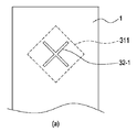
図4は、本発明の一実施形態による二重帯域二重偏波移動通信基地局アンテナの平面図であり、図5は、図4のA−A’部分の一部透過切断面図である。図6は、図4の第1の放射素子の給電構造を示した平面及び背面図であり、図7は、図6の斜視図として、図6及び図7では、説明の便宜のために、第1の放射素子スロット構造及び給電用導体パターンが形成された回路基板を示し、それ以外の構成に対しては省略する。 4 is a plan view of a dual-band dual-polarization mobile communication base station antenna according to an embodiment of the present invention, and FIG. 5 is a partially transparent cutaway view of the AA ′ portion of FIG. . 6 is a plan view and a rear view showing the feeding structure of the first radiating element of FIG. 4, FIG. 7 is a perspective view of FIG. 6, and FIG. 6 and FIG. The circuit board on which the first radiating element slot structure and the power supply conductor pattern are formed is shown, and the other configurations are omitted.
図4乃至図7を参照すると、本発明の一実施形態によるアンテナは、第1の周波数帯域(例えば、700/800MHz帯域)のいわゆる、スロットタイプの第1の放射素子31、32が反射板1の上面に一定間隔で配置されている。また、第2の周波数帯域(例えば、1.8/2GHz帯域)のダイポールタイプの第2の放射素子21、22、23、24は、第1の放射素子31、32に積層されるかまたは第1の放射素子31、32間で反射板1の上面に直接設置される。
4 to 7, an antenna according to an embodiment of the present invention includes so-called slot-type first radiating
第1の放射素子31、32の各々は、本発明の特徴によって反射板1自体に全体的にX字の穴形態で直接的に形成され、相互直交するX字形態の二重偏波の送信信号を発生するためのスロット構造31−1と、スロット構造31−1の上面で設置されるアルミニウム(銀メッキ)または銅(銀メッキ)のような金属材質のパッチ板31−2、32−2で構成される。パッチ板31−2、32−2は、スロット構造31−1の放射特性を最適化するために適切な形態及びサイズを有し、下部の反射板1から絶縁されるようにプラスチック素材などの支持台を利用して設置される。すなわち、本発明では、反射板1自体がスロット構造を形成する金属板の役割をするようになる。
Each of the
スロット構造31−1は、反射板1の裏面に付着される回路基板311に予め適切な導体パターンで形成される給電用ストリップ線路(図6の3111)とカップリング方式で給電信号の提供を受ける。回路基板311は、通常的なPCB基板形態で形成され得る。
The slot structure 31-1 is provided with a feeding signal in a coupling manner with a feeding strip line (3111 in FIG. 6) formed in advance with an appropriate conductor pattern on a
X字形態のスロット構造31−1で、X字形態の二重偏波のうち一偏波を各々発生する‘/’字または‘\’字スロットは、各々該当第1の周波数帯域(2GHz)の周波数波長を考慮し、例えば2/λに対応するようにその長さが形成されることができる。この場合に、それぞれのスロットの長さは、例えば、約160mm、それぞれのスロットの幅は、例えば、約2mmに設計されることができる。 In the X-shaped slot structure 31-1, the '/'-shaped or '\'-shaped slots that respectively generate one of the X-shaped dual polarized waves are respectively corresponding to the first frequency band (2 GHz). For example, the length can be formed to correspond to 2 / λ. In this case, the length of each slot can be designed to be about 160 mm, for example, and the width of each slot can be designed to be about 2 mm, for example.
X字形態で形成される二重偏波でそれぞれの偏波を発生するストリップ線路3111を回路基板311に形成する場合に、相互交差するように(しかし、電気的に接続されないように)導体パターンを形成しなければならない部位があるが、図6の(b)でA部分にその側面構造を拡大して示したように、相互交差する部位に導体パターンのうち一つの導体パターンをエアブリッジ構造で形成する。
Conductor patterns so as to cross each other (but not to be electrically connected) when the
一方、このように形成される第1の放射素子31、32に積層される第2の放射素子21、22は、第1の放射素子31、32のパッチ板31−2、32−2上に設置され、パッチ板31−2、32−2を接地端として使用するようになる。すなわち、第2の放射素子21、22は、パッチ板31−2、32−2により接地される。第1の放射素子31、32に積層される第2の放射素子21、22は、第1の放射素子31、32のパッチ板31−2、32−2及び反射板1を貫通する給電ケーブル212を介して給電網と接続される。
On the other hand, the
上記のような構造によって、本発明によるアンテナで、回路基板311の給電用ストリップ線路3111に印加される送信信号は、回路基板311自体の誘電層を経てスロット構造31−1にカップリングされ、これによってスロット構造31−1には、送信信号の電気場(E field)が形成される。スロット構造31−1に形成される送信信号の電気場は、以後、適正な間隔をおいて離隔されるように固定されたパッチ板31−2、32−2を経て放射される。
With the structure as described above, the transmission signal applied to the
上記の構造を有する本発明による第1及び第2の放射素子の積層配置方式では、従来の上部及び下部パッチ板を有する構造と比較して、一つパッチ板のみを具備するので、第1の放射素子に積層され設置される第2の放射素子と、単独で設置される第2の放射素子との高さ差が減るようになる。例えば、本発明で第1の放射素子に積層され設置される第2の放射素子と、単独で設置される第2の放射素子との間の高さ差は、約25mmであり得る。このように、高さ差が減るようになるので、高さ差を有する第2の放射素子の間により発生される位相遅延(phase delay)が従来と比較して減るようになり、アンテナダウンチルトの時、水平ビーム幅の減少量が減るようになる。 Since the first and second radiating elements according to the present invention having the above structure have only one patch plate as compared with the conventional structure having upper and lower patch plates, The height difference between the second radiating element stacked and installed on the radiating element and the second radiating element installed alone is reduced. For example, the height difference between the second radiating element stacked and installed on the first radiating element in the present invention and the second radiating element installed alone may be about 25 mm. As described above, since the height difference is reduced, the phase delay generated between the second radiating elements having the height difference is reduced as compared with the conventional case, and the antenna downtilt is performed. At this time, the reduction amount of the horizontal beam width is reduced.
また、この場合に、本発明によるアンテナは、従来と比較して第1の放射素子及びこれに積層され設置される第2の放射素子の高さが低くなるので、全体的なアンテナの高さを低めるようになって、従来と比較してより小型、軽量化を満足させるようになる。 In this case, the antenna according to the present invention has a lower overall height than the conventional antenna because the first radiating element and the second radiating element stacked and installed thereon are lower. As a result, the size and weight are reduced as compared with the prior art.
また、第1の放射素子に積層され設置される第2の放射素子は、第1の放射素子のパッチ板を接地端として使用するようになるが、本発明では、第1の放射素子のパッチ板は、スロット構造の部位より大きく形成されるので、従来と比較して大きなサイズで設計することが可能になる。したがって、本発明によるパッチ板は、その上に積層されるダイポールタイプの第2の放射素子で要求される接地面積を満足させるようになり、第2の放射素子で無線周波数のパターン特性劣化を防止することができるようになる。 Further, the second radiating element that is stacked and installed on the first radiating element uses the patch plate of the first radiating element as a ground terminal. In the present invention, the patch of the first radiating element is used. Since the plate is formed larger than the portion of the slot structure, it is possible to design the plate with a size larger than the conventional one. Accordingly, the patch plate according to the present invention satisfies the grounding area required for the dipole type second radiating element laminated thereon, and prevents deterioration of the radio frequency pattern characteristics by the second radiating element. Will be able to.
上記のように、本発明の一実施形態による移動通信基地局アンテナの構成及び動作がなされることができ、一方、本発明の説明では、具体的な実施形態に関して説明したが、添付した特許請求の範囲により規定されるような本発明の精神及び範囲を外れることなく、形式や細部の様々な変更が可能であることは、当該技術分野における通常の知識を持つ者には明らかである。 As described above, the configuration and operation of a mobile communication base station antenna according to an embodiment of the present invention can be performed, while the description of the present invention has been described with reference to a specific embodiment, but the appended claims It will be apparent to those skilled in the art that various modifications in form and detail can be made without departing from the spirit and scope of the invention as defined by the scope of the invention.
例えば、上記の説明では、第1の放射素子に積層されるように設置される第2の放射素子がダイポールタイプであることを例に上げて説明したが、この他にも本発明の他の実施形態では、第1の放射素子に積層される第2の放射素子が通常的なパッチタイプの構造で構成することもできる。 For example, in the above description, the second radiating element installed so as to be stacked on the first radiating element has been described as an example of a dipole type. In the embodiment, the second radiating element stacked on the first radiating element may be configured with a normal patch type structure.
また、上記の説明では、第1の放射素子に第2の放射素子が積層される場合を一例として説明したが、この他にも本発明の他の実施形態では、第2の放射素子が積層されなく、本発明による構造を有する第1の放射素子が別途に設置されるようにする構成も可能である。 In the above description, the case where the second radiating element is stacked on the first radiating element has been described as an example. However, in another embodiment of the present invention, the second radiating element is stacked. Alternatively, a configuration in which the first radiating element having the structure according to the present invention is separately installed is also possible.
1 反射板
11 第1の放射素子
11−1 下部パッチ板
11−2 上部パッチ板
12 第1の放射素子
12−1 下部パッチ板
12−2 上部パッチ板
21、22、23、24 第2の放射素子
31 第1の放射素子
31−1 スロット構造
31−2 パッチ板
32 第1の放射素子
32−2 パッチ板
111 回路基板
112 給電ケーブル
212 給電ケーブル
311 回路基板
3111 ストリップ線路
DESCRIPTION OF
Claims (4)
反射板と、
前記反射板上に形成される第1の周波数帯域の第1の放射素子と、を含み、
前記第1の放射素子は、
前記反射板自体に全体的にX字の穴形態で直接的に形成され、相互直交するX字形態の二重偏波の送信信号を発生するためのスロット構造と、
前記スロット構造の上面で前記反射板から絶縁されるように設置される金属材質のパッチ板と、を含むことを特徴とする移動通信基地局アンテナ。 A mobile communication base station antenna,
A reflector,
A first radiating element of a first frequency band formed on the reflector,
The first radiating element includes:
A slot structure for generating dual-polarized transmission signals in the form of X-shaped holes which are directly formed in the shape of X-shaped holes on the reflector itself and orthogonal to each other;
A mobile communication base station antenna comprising: a patch plate made of a metal material so as to be insulated from the reflection plate on an upper surface of the slot structure.
Applications Claiming Priority (3)
| Application Number | Priority Date | Filing Date | Title |
|---|---|---|---|
| KR1020120137888A KR20140069968A (en) | 2012-11-30 | 2012-11-30 | Antenna of mobile communication station |
| KR10-2012-0137888 | 2012-11-30 | ||
| PCT/KR2013/010990 WO2014084655A1 (en) | 2012-11-30 | 2013-11-29 | Antenna for mobile-communication base station |
Publications (1)
| Publication Number | Publication Date |
|---|---|
| JP2015536626A true JP2015536626A (en) | 2015-12-21 |
Family
ID=50828199
Family Applications (1)
| Application Number | Title | Priority Date | Filing Date |
|---|---|---|---|
| JP2015545366A Withdrawn JP2015536626A (en) | 2012-11-30 | 2013-11-29 | Mobile communication base station antenna |
Country Status (6)
| Country | Link |
|---|---|
| US (1) | US20150263431A1 (en) |
| EP (1) | EP2928020A4 (en) |
| JP (1) | JP2015536626A (en) |
| KR (1) | KR20140069968A (en) |
| CN (1) | CN104798257A (en) |
| WO (1) | WO2014084655A1 (en) |
Families Citing this family (16)
| Publication number | Priority date | Publication date | Assignee | Title |
|---|---|---|---|---|
| KR101609665B1 (en) * | 2014-11-11 | 2016-04-06 | 주식회사 케이엠더블유 | Antenna of mobile communication station |
| CN104393422B (en) * | 2014-11-17 | 2018-05-01 | 京信通信系统(中国)有限公司 | Multi-frequency array antenna |
| KR101712375B1 (en) * | 2015-11-20 | 2017-03-07 | 주식회사 에이스테크놀로지 | Antenna for sticking the ceiling for decreasing beam tilt difference depend on frequency band |
| US11038272B2 (en) * | 2017-05-29 | 2021-06-15 | Huawei Technologies Co., Ltd. | Configurable antenna array with diverse polarizations |
| CN107257018B (en) * | 2017-06-06 | 2018-08-14 | 江苏亨鑫科技有限公司 | Low frequency radiating element and multifrequency antenna with the low frequency radiating element |
| CN107359415B (en) * | 2017-06-08 | 2020-12-15 | 京信通信技术(广州)有限公司 | Multi-frequency antenna |
| CN108539434A (en) * | 2018-04-17 | 2018-09-14 | 昆山恩电开通信设备有限公司 | A kind of ultra wide band low cost radiating element and antenna |
| US11101565B2 (en) * | 2018-04-26 | 2021-08-24 | Neptune Technology Group Inc. | Low-profile antenna |
| US10797408B1 (en) * | 2019-04-18 | 2020-10-06 | Huawei Technologies Co., Ltd. | Antenna structure and method for manufacturing the same |
| CN110444858B (en) * | 2019-07-29 | 2021-09-07 | 中信科移动通信技术股份有限公司 | Method for improving index, antenna array and base station antenna |
| CN112531356B (en) | 2019-09-18 | 2022-05-03 | 北京小米移动软件有限公司 | Antenna structure and mobile terminal |
| US11431110B2 (en) * | 2019-09-30 | 2022-08-30 | Qualcomm Incorporated | Multi-band antenna system |
| KR102158981B1 (en) * | 2019-11-18 | 2020-09-23 | 주식회사 에이스테크놀로지 | Antenna with a symmetrical Feeder Circuit for Improving Antenna Pattern |
| KR20220036601A (en) | 2020-09-16 | 2022-03-23 | 삼성전기주식회사 | Antenna apparatus |
| KR20220037913A (en) * | 2020-09-18 | 2022-03-25 | 삼성전자주식회사 | Antenna structure and electronic device including the same |
| US11843187B2 (en) * | 2021-04-26 | 2023-12-12 | Amazon Technologies, Inc. | Antenna module grounding for phased array antennas |
Family Cites Families (14)
| Publication number | Priority date | Publication date | Assignee | Title |
|---|---|---|---|---|
| US5872544A (en) * | 1997-02-04 | 1999-02-16 | Gec-Marconi Hazeltine Corporation Electronic Systems Division | Cellular antennas with improved front-to-back performance |
| DE19823750A1 (en) * | 1998-05-27 | 1999-12-09 | Kathrein Werke Kg | Antenna array with several primary radiator modules arranged vertically one above the other |
| SE9802883L (en) * | 1998-08-28 | 2000-02-29 | Ericsson Telefon Ab L M | Antenna device |
| EP1247311A1 (en) * | 1999-12-01 | 2002-10-09 | Allgon AB | An antenna assembly and a method of mounting an antenna assembly |
| JP2003046326A (en) * | 2001-08-01 | 2003-02-14 | Denki Kogyo Co Ltd | Polarized wave sharing antenna |
| JP4112456B2 (en) * | 2003-07-29 | 2008-07-02 | 電気興業株式会社 | Polarized antenna device |
| CN2879453Y (en) * | 2005-08-30 | 2007-03-14 | 杨华 | Plate type mobile communication base station antenna |
| KR100944624B1 (en) | 2008-04-18 | 2010-02-26 | 경희대학교 산학협력단 | Glare Tester for sunlight and artificial lighting |
| KR101085887B1 (en) * | 2008-12-22 | 2011-11-23 | 주식회사 케이엠더블유 | Dual-band dual-polarized base station antenna for mobile communication |
| CN101826658B (en) * | 2009-03-03 | 2013-04-17 | 华为技术有限公司 | Reflecting board of base station antenna and base station antenna |
| KR101125180B1 (en) * | 2009-11-17 | 2012-03-19 | 주식회사 케이엠더블유 | Method for installing radiator elements arranged in different planes and antenna thereof |
| JP4866962B2 (en) * | 2010-04-22 | 2012-02-01 | アルプス電気株式会社 | Antenna device |
| KR101144528B1 (en) * | 2010-08-31 | 2012-05-11 | 주식회사 에이스테크놀로지 | A patch antenna synchronous generating linearly polarized wave and circularly polarized wave |
| CN202076403U (en) * | 2011-05-16 | 2011-12-14 | 摩比天线技术(深圳)有限公司 | Double-frequency dual-polarization antenna oscillator of loading filter |
-
2012
- 2012-11-30 KR KR1020120137888A patent/KR20140069968A/en not_active Application Discontinuation
-
2013
- 2013-11-29 CN CN201380062404.7A patent/CN104798257A/en active Pending
- 2013-11-29 WO PCT/KR2013/010990 patent/WO2014084655A1/en active Application Filing
- 2013-11-29 EP EP13859174.8A patent/EP2928020A4/en not_active Withdrawn
- 2013-11-29 JP JP2015545366A patent/JP2015536626A/en not_active Withdrawn
-
2015
- 2015-05-27 US US14/723,217 patent/US20150263431A1/en not_active Abandoned
Also Published As
| Publication number | Publication date |
|---|---|
| WO2014084655A1 (en) | 2014-06-05 |
| EP2928020A1 (en) | 2015-10-07 |
| US20150263431A1 (en) | 2015-09-17 |
| KR20140069968A (en) | 2014-06-10 |
| CN104798257A (en) | 2015-07-22 |
| EP2928020A4 (en) | 2016-07-20 |
Similar Documents
| Publication | Publication Date | Title |
|---|---|---|
| US10622706B2 (en) | Mobile communication base station antenna | |
| JP2015536626A (en) | Mobile communication base station antenna | |
| US10910700B2 (en) | Omnidirectional antenna for mobile communication service | |
| JP5712964B2 (en) | Antenna device | |
| JP5645949B2 (en) | Method of installing radiating elements arranged on different planes and antenna using the same | |
| US7755559B2 (en) | Dual-band omnidirectional antenna | |
| JPWO2008050441A1 (en) | Antenna device | |
| JP4819153B2 (en) | Dual polarization antenna | |
| CN109478721B (en) | Antenna, device with one or more antennas and communication device | |
| KR20120086841A (en) | Base station antenna structure having multi-band dipole element array improved in isolation-characteristics | |
| KR101644445B1 (en) | Base station antenna | |
| JP4905239B2 (en) | Antenna device | |
| JP4139837B2 (en) | Dual frequency dipole antenna device | |
| JP5514779B2 (en) | Dual polarization antenna | |
| JP5496967B2 (en) | Dual-frequency antenna | |
| JP5078732B2 (en) | Antenna device | |
| JP3782278B2 (en) | Beam width control method of dual-polarized antenna | |
| JP2011087241A (en) | Antenna, and array antenna | |
| JP4950155B2 (en) | Dipole horizontal array antenna device | |
| JP2005203841A (en) | Antenna apparatus | |
| TW201208197A (en) | High gain loop array antenna system and electronic device | |
| JP2009005104A (en) | High frequency circuit and antenna | |
| JP2006157845A (en) | Antenna device | |
| JP2007135038A (en) | Dipole horizontal array antenna device | |
| KR20120086842A (en) | Base station antenna structure having multi-band dipole element array |
Legal Events
| Date | Code | Title | Description |
|---|---|---|---|
| A977 | Report on retrieval |
Free format text: JAPANESE INTERMEDIATE CODE: A971007 Effective date: 20160620 |
|
| A761 | Written withdrawal of application |
Free format text: JAPANESE INTERMEDIATE CODE: A761 Effective date: 20160624 |