KR20140069968A - Antenna of mobile communication station - Google Patents
Antenna of mobile communication station Download PDFInfo
- Publication number
- KR20140069968A KR20140069968A KR1020120137888A KR20120137888A KR20140069968A KR 20140069968 A KR20140069968 A KR 20140069968A KR 1020120137888 A KR1020120137888 A KR 1020120137888A KR 20120137888 A KR20120137888 A KR 20120137888A KR 20140069968 A KR20140069968 A KR 20140069968A
- Authority
- KR
- South Korea
- Prior art keywords
- radiating element
- mobile communication
- antenna
- reflector
- base station
- Prior art date
Links
Images


Classifications
-
- H—ELECTRICITY
- H01—ELECTRIC ELEMENTS
- H01Q—ANTENNAS, i.e. RADIO AERIALS
- H01Q13/00—Waveguide horns or mouths; Slot antennas; Leaky-waveguide antennas; Equivalent structures causing radiation along the transmission path of a guided wave
- H01Q13/10—Resonant slot antennas
- H01Q13/106—Microstrip slot antennas
-
- H—ELECTRICITY
- H01—ELECTRIC ELEMENTS
- H01Q—ANTENNAS, i.e. RADIO AERIALS
- H01Q5/00—Arrangements for simultaneous operation of antennas on two or more different wavebands, e.g. dual-band or multi-band arrangements
-
- H—ELECTRICITY
- H01—ELECTRIC ELEMENTS
- H01Q—ANTENNAS, i.e. RADIO AERIALS
- H01Q1/00—Details of, or arrangements associated with, antennas
- H01Q1/12—Supports; Mounting means
- H01Q1/22—Supports; Mounting means by structural association with other equipment or articles
- H01Q1/24—Supports; Mounting means by structural association with other equipment or articles with receiving set
- H01Q1/241—Supports; Mounting means by structural association with other equipment or articles with receiving set used in mobile communications, e.g. GSM
- H01Q1/246—Supports; Mounting means by structural association with other equipment or articles with receiving set used in mobile communications, e.g. GSM specially adapted for base stations
-
- H—ELECTRICITY
- H01—ELECTRIC ELEMENTS
- H01Q—ANTENNAS, i.e. RADIO AERIALS
- H01Q21/00—Antenna arrays or systems
- H01Q21/06—Arrays of individually energised antenna units similarly polarised and spaced apart
- H01Q21/08—Arrays of individually energised antenna units similarly polarised and spaced apart the units being spaced along or adjacent to a rectilinear path
-
- H—ELECTRICITY
- H01—ELECTRIC ELEMENTS
- H01Q—ANTENNAS, i.e. RADIO AERIALS
- H01Q21/00—Antenna arrays or systems
- H01Q21/24—Combinations of antenna units polarised in different directions for transmitting or receiving circularly and elliptically polarised waves or waves linearly polarised in any direction
- H01Q21/26—Turnstile or like antennas comprising arrangements of three or more elongated elements disposed radially and symmetrically in a horizontal plane about a common centre
-
- H—ELECTRICITY
- H01—ELECTRIC ELEMENTS
- H01Q—ANTENNAS, i.e. RADIO AERIALS
- H01Q21/00—Antenna arrays or systems
- H01Q21/30—Combinations of separate antenna units operating in different wavebands and connected to a common feeder system
-
- H—ELECTRICITY
- H01—ELECTRIC ELEMENTS
- H01Q—ANTENNAS, i.e. RADIO AERIALS
- H01Q5/00—Arrangements for simultaneous operation of antennas on two or more different wavebands, e.g. dual-band or multi-band arrangements
- H01Q5/40—Imbricated or interleaved structures; Combined or electromagnetically coupled arrangements, e.g. comprising two or more non-connected fed radiating elements
- H01Q5/42—Imbricated or interleaved structures; Combined or electromagnetically coupled arrangements, e.g. comprising two or more non-connected fed radiating elements using two or more imbricated arrays
-
- H—ELECTRICITY
- H01—ELECTRIC ELEMENTS
- H01Q—ANTENNAS, i.e. RADIO AERIALS
- H01Q9/00—Electrically-short antennas having dimensions not more than twice the operating wavelength and consisting of conductive active radiating elements
- H01Q9/04—Resonant antennas
- H01Q9/0407—Substantially flat resonant element parallel to ground plane, e.g. patch antenna
- H01Q9/0414—Substantially flat resonant element parallel to ground plane, e.g. patch antenna in a stacked or folded configuration
-
- H—ELECTRICITY
- H01—ELECTRIC ELEMENTS
- H01Q—ANTENNAS, i.e. RADIO AERIALS
- H01Q9/00—Electrically-short antennas having dimensions not more than twice the operating wavelength and consisting of conductive active radiating elements
- H01Q9/04—Resonant antennas
- H01Q9/0407—Substantially flat resonant element parallel to ground plane, e.g. patch antenna
- H01Q9/0428—Substantially flat resonant element parallel to ground plane, e.g. patch antenna radiating a circular polarised wave
- H01Q9/0435—Substantially flat resonant element parallel to ground plane, e.g. patch antenna radiating a circular polarised wave using two feed points
-
- H—ELECTRICITY
- H01—ELECTRIC ELEMENTS
- H01Q—ANTENNAS, i.e. RADIO AERIALS
- H01Q9/00—Electrically-short antennas having dimensions not more than twice the operating wavelength and consisting of conductive active radiating elements
- H01Q9/04—Resonant antennas
- H01Q9/0407—Substantially flat resonant element parallel to ground plane, e.g. patch antenna
- H01Q9/045—Substantially flat resonant element parallel to ground plane, e.g. patch antenna with particular feeding means
- H01Q9/0457—Substantially flat resonant element parallel to ground plane, e.g. patch antenna with particular feeding means electromagnetically coupled to the feed line
Landscapes
- Physics & Mathematics (AREA)
- Electromagnetism (AREA)
- Engineering & Computer Science (AREA)
- Computer Networks & Wireless Communication (AREA)
- Variable-Direction Aerials And Aerial Arrays (AREA)
- Aerials With Secondary Devices (AREA)
- Waveguide Aerials (AREA)
Abstract
Description
본 발명은 이동통신 시스템에 사용되는 이동통신 기지국 안테나에 관한 것으로, 특히, 이중대역(dual band) 이중편파 구조의 안테나에 채용되기에 적합한 이동통신 기지국 안테나에 관한 것이다.BACKGROUND OF THE
이동통신 시스템에 사용되는 중계기를 비롯한 기지국 안테나는 다양한 형태와 구조가 있을 수 있으며, 통상, 길이방향으로 직립하는 적어도 하나의 반사판 상에 다수의 방사소자들이 적절히 배치되는 구조를 가진다.A base station antenna including a repeater used in a mobile communication system may have various shapes and structures, and typically has a structure in which a plurality of radiating elements are appropriately disposed on at least one reflector standing upright in the longitudinal direction.
최근, 기지국 안테나에 대한 소형화 및 경량화 요구를 만족시키고자 다양한 연구가 이루어지고 있으며, 이들 중에서 이중대역 이중편파 안테나의 경우에는 예를 들어, 700/800MHz 대역의 저주파수 대역의 제1방사소자에 예를 들어, 차세대 무선 서비스 대역(AWS: Advanced Wireless Service 대역) 또는 2GHz 대역의 고주파수 대역의 제2방사소자를 적층한(stack) 구조의 안테나가 개발되고 있다. In recent years, various researches have been conducted to satisfy demands for downsizing and weight reduction of base station antennas. Of these, dual-band dual polarized antennas, for example, include a first radiating element in a low frequency band of 700/800 MHz For example, an antenna having a structure in which a second radiating element of a next-generation wireless service band (AWS: Advanced Wireless Service band) or a high-frequency band of 2 GHz band is stacked is being developed.
이러한 안테나는 예를 들어, 패치(patch) 타입의 제1방사소자 위에 패치 타입 또는 다이폴(dipole) 타입의 제2방사소자가 설치된 적층 구조의 제1, 제2방사소자들을 가질 수 있는데, 이러한 적층 구조의 제1, 제2방사소자들은 제1주파수 대역의 방사소자 배열을 만족시키기 위한 간격으로 다수개가 반사판 상에 배치된 구조를 가질 수 있다.Such an antenna may have a laminated structure of first and second radiating elements in which, for example, a patch type or dipole type second radiating element is mounted on a first radiating element of a patch type, The first and second radiation elements of the structure may have a structure in which a plurality of radiation elements are arranged on the reflection plate at intervals to satisfy the radiation element arrangement of the first frequency band.
또한, 이와 같이 다수 개 설치된 적층 구조의 제1, 제2방사소자 사이에는 해당 제2주파수 대역의 방사소자 배열을 만족시키기 위해 제2방사소자가 반사판 상에 추가적으로 설치되는 구조를 가진다. 이러한 배치 방식으로 인해, 전체적으로 소형화를 만족시키면서 안테나 이득을 얻을 수 있게 된다. In addition, the second radiating element is additionally provided on the reflector between the first and second radiating elements of the laminated structure having the plurality of antennas so as to satisfy the radiating element arrangement of the second frequency band. With this arrangement, the antenna gain can be obtained while satisfying the miniaturization as a whole.
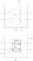
도 1은 종래의 이중대역 이중편파 이동통신 기지국 안테나의 일 예시 평면도이며, 도 2는 도 1의 A-A'부분 일부 투과 절단면도이다. 도 1 및 도 2를 참조하여 제1방사소자에 제2방사소자가 적층된 구조를 구비한 안테나를 살펴보면, 제1주파수 대역(예를 들어, 700/800MHz 대역)의 패치 타입 제1방사소자들(11, 12)이 반사판(1) 상면에 일정 간격으로 배치되어 있다. 또한, 제2주파수 대역(예를 들어, AWS 대역)의 다이폴 타입 제2방사소자들(21, 22, 23, 24)들은 상기 제1방사소자들(11, 12)에 적층되거나 또는 제1방사소자들(11, 12) 사이에서 반사판(1) 상면에 직접 설치된다. FIG. 1 is a plan view of a conventional dual-band dual polarization mobile communication base station antenna, and FIG. 2 is a partially cutaway cross-sectional view taken along a line A-A 'in FIG. Referring to FIGS. 1 and 2, an antenna having a structure in which a second radiating element is laminated on a first radiating element includes a patch type first radiating element (first antenna) having a first frequency band (for example, 700/800 MHz band) (11, 12) are arranged at regular intervals on the upper surface of the reflection plate (1). Further, the dipole-type second
제1방사소자들(11, 12) 각각은 상부 패치 판(11-2, 12-2) 및 하부 패치 판(11-1, 12-1)으로 구성된다. 하부 패치 판(11-1, 12-1)들은 반사판(1)을 관통하는 급전 케이블(112)을 통해서 반사판(1)의 뒷면에 부착되는 급전용 도체 패턴이 형성된 회로기판(111)과 연결된다. 또한, 상기 제1방사소자들(11, 12)에 적층된 제2방사소자들(21, 22)은 반사판(1) 및 해당 설치된 제1방사소자들(11, 12)의 상부 및 하부 패치 판(11-1, 11-2)을 관통하는 급전 케이블(212)을 통해서 급전망과 연결된다.Each of the first
한편, 도 3에는 도 1의 제1방사소자들의 급전 구조를 나타낸 도면으로서, 도 3의 (a)는 평면도이며, 도 3의 (b)는 배면도이다. 도 3에서는 설명의 편의를 위해 제1방사소자들 중 하나의 하부 패치 판(11-1) 및 급전용 도체 패턴이 형성된 회로기판(111)을 나타내었으며, 그 외의 구성에 대해서는 생략하였다. 도 1 내지 도 3을 참조하면, 제1방사소자(11)의 하부 패치 판(11-1)은 반사판(1)을 관통하는 급전 케이블(112)을 통해서 반사판(1)의 뒷면에 부착되는 회로기판(111)과 연결된다. 즉, 제1방사소자의 급전용 도체 패턴은 회로기판(111) 상에서 인쇄 방식으로 형성되며, 인쇄회로기판(111)에서 급전 포인트들(a~d)과, 하부 패치 판(11-1)의 급전 포인트들(a~d)은 급전 케이블들(112)을 통해 연결되는 구조를 가진다.FIG. 3 is a plan view showing the feeding structure of the first radiating elements of FIG. 1. FIG. 3 (a) is a plan view and FIG. 3 (b) is a rear view. In FIG. 3, one of the first radiating elements is a lower patch plate 11-1 and a
이때, 예를 들어, a 급전 포인트에 비해 이와 대각선에 위치하는 c 급전 포인트에서의 송신 신호는 180도 위상 지연되며, 마찬가지로, b 급전 포인트에 비해 이와 대각선에 위치하는 d 급전 포인트에서의 송신 신호도 180도 위상 지연되도록 회로 기판(111)에서 급전용 도체 패턴이 형성된다. 이에 따라, 제1방사소자의 하부 패치 판(11-1)에서 a, c 급전 포인트 및 b, d 급전 포인트에서 서로 직교하는 이중 편파가 발생하게 된다. 한편, 제1방사소자의 상부 패치 판(11-2)은 방사 특성 최적화를 위해 설치되는 것으로서, 하부 패치 판(11-1)과 절연되게 플라스틱 소재 등의 지지대를 이용하여 설치된다.At this time, for example, the transmitted signal at the c feed point located diagonal to the a feed point is delayed by 180 degrees relative to the a feed point, and the transmitted signal at the d feed point located diagonally to the b feed point A feed conductor pattern is formed on the
상기한 구조를 가지는 기지국 안테나에 관한 기술로는, 본원 출원인에 의해 선출원된 국내 특허 출원번호 제10-2009-0110696호(명칭: 서로 다른 평면에 배치되는 방사소자들의 설치 방법 및 이를 이용한 안테나, 발명자: 문영찬 외 4명, 출원일: 2009년 11월 17일)에 개시된 바를 예로 들 수 있다.As a technique related to the base station antenna having the above-described structure, there is disclosed in Korean Patent Application No. 10-2009-0110696 (titled: installation method of radiating elements arranged on different planes, antenna using the same, : Yeon Chan Moon, et al., Filed on November 17, 2009).
그런데, 이러한 제1, 제2방사소자의 배치 방식에서는, 제1방사소자에 적층되어 설치되는 제2방사소자와, 단독으로 설치되는 제2방사소자들이 서로 다른 평면에 설치됨으로써, 제2주파수 대역의 신호가 방사될 경우에 위상 차이가 발생하게 되는 문제점이 있었다. 예를 들어, 제1방사소자에 적층되어 설치되는 제2방사소자와, 단독으로 설치되는 제2방사소자들 간의 높이 차이는 약 50mm일 수 있다. 높이 차이를 가지는 제2방사소자들 간에 의해 발생되는 위상 지연(phase delay)으로 인해, 안테나 다운 틸트시 수평 빔폭 감소량이 증가하게 된다.However, in the first and second arrangements of the first and second radiating elements, the second radiating elements and the second radiating elements, which are installed on the first radiating element, are provided on different planes, There is a problem that a phase difference occurs. For example, the height difference between the second radiating element, which is stacked and installed on the first radiating element, and the second radiating elements that are installed alone, may be about 50 mm. Due to the phase delay generated between the second radiating elements having a height difference, the horizontal beam width reduction amount increases at the antenna down-tilt.
또한, 제1방사소자에 적층되어 설치되는 제2방사소자는 패치 타입의 제1방사소자의 상부 패치 판을 접지단으로 사용하게 된다. 그런데, 제1방사소자의 상부 패치 판은 방사 특성을 만족하기 위해 하부 패치 판에 비해 작은 사이즈로 설계되므로, 다이폴 타입의 제2방사소자에서 요구되는 접지 면적을 만족시키기가 어렵게 된다. 이와 같이, 접지 면적 불충분으로 인해 제2방사소자에서 무선 주파수의 패턴 특성 열화가 발생할 수 있다.Further, the second radiating element which is stacked and installed on the first radiating element uses the upper patch plate of the patch type first radiating element as the grounding end. However, since the upper patch plate of the first radiating element is designed to have a smaller size than the lower patch plate to satisfy the radiation characteristic, it is difficult to satisfy the grounding area required by the dipole-type second radiating element. In this way, the pattern characteristic deterioration of the radio frequency may occur in the second radiating element due to insufficient grounding area.
따라서, 본 발명의 목적은 전체 안테나의 사이즈를 줄일 수 있으며, 특히, 제1주파수 대역의 제1방사소자에 적층되어 설치되는 제2주파수 대역의 제2방사소자와, 단독으로 설치되는 제2주파수 대역의 제2방사소자를 구비한 이중대역 안테나에서, 제2방사소자들 간의 높이 차이를 줄일 수 있으며, 제1방사소자에 적층되어 설치되는 제2방사소자에서 요구되는 접지 면적을 충분히 확보할 수 있으며, 방사 특성을 향상시킬 수 있는 이동통신 기지국 안테나를 제공함에 있다.SUMMARY OF THE INVENTION Accordingly, it is an object of the present invention to reduce the size of an entire antenna and, in particular, to provide a second radiating element of a second frequency band which is stacked and installed on a first radiating element of a first frequency band, In the dual band antenna having the second radiating element of the first radiating element, the height difference between the second radiating elements can be reduced, and the grounding area required in the second radiating element which is stacked and installed on the first radiating element can be sufficiently secured And it is an object of the present invention to provide a mobile communication base station antenna capable of improving radiation characteristics.
상기한 목적을 달성하기 위하여 본 발명은 이동통신 기지국 안테나에 있어서, 반사판과; 상기 반사판 상에 형성되는 제1주파수 대역의 제1방사소자를 포함하며; According to an aspect of the present invention, there is provided a mobile communication base station antenna comprising: a reflection plate; A first radiating element of a first frequency band formed on the reflector;
상기 제1방사소자는 상기 반사판 자체에 전체적으로 X자의 구멍 형태로 직접적으로 형성되어, 서로 직교하는 X자 형태의 이중편파의 송신 신호를 발생하기 위한 슬롯 구조와; 상기 슬롯 구조의 상면에서 상기 반사판과 절연되게 설치되는 금속 재질의 패치 판을 포함함을 특징으로 한다.Wherein the first radiating element is formed directly on the reflector itself as an X-shaped hole to generate transmission signals of an X-shaped dual polarized wave orthogonal to each other; And a patch plate made of metal and disposed on the upper surface of the slot structure so as to be insulated from the reflection plate.
상기한 바와 같이, 본 발명에 따른 이동통신 기지국 안테나는 전체 안테나의 사이즈를 줄일 수 있으며, 특히, 제1주파수 대역의 제1방사소자에 적층되어 설치되는 제2주파수 대역의 제2방사소자와, 단독으로 설치되는 제2주파수 대역의 제2방사소자를 구비한 이중대역 안테나에서, 서로간의 높이 차이를 줄일 수 있으며, 제1방사소자에 적층되어 설치되는 제2방사소자에서 요구되는 접지 면적을 충분히 확보할 수 있으며, 방사 특성을 향상시킬 수 있게 된다.As described above, the mobile communication base station antenna according to the present invention can reduce the size of the entire antenna. In particular, the mobile communication base station antenna includes a second radiating element in a second frequency band, which is stacked on a first radiating element in a first frequency band, In the dual band antenna having the second radiating element in the second frequency band which is installed alone, the height difference between them can be reduced, and the grounding area required in the second radiating element which is stacked and installed on the first radiating element And it is possible to improve the radiation characteristic.
도 1은 종래의 이중대역 이중편파 이동통신 기지국 안테나의 일 예시 평면도
도 2는 도 1의 A-A'부분 일부 투과 절단면도
도 3은 도 1의 제1방사소자들의 급전 구조를 나타낸 평면 및 배면도
도 4는 본 발명의 일 실시예에 따른 이중대역 이중편파 이동통신 기지국 안테나의 평면도
도 5는 도 4의 A-A'부분 일부 투과 절단면도
도 6은 도 4의 제1방사소자의 급전 구조를 나타낸 평면 및 배면도
도 7은 도 6의 사시도1 is a plan view of an example of a conventional dual-band dual polarization mobile communication base station antenna
Fig. 2 is a cross-sectional view taken along the line A-A '
Fig. 3 is a plan view showing a feeding structure of the first radiating elements of Fig. 1 and a rear view
4 is a plan view of a dual band dual polarization mobile communication base station antenna according to an embodiment of the present invention.
5 is a cross-sectional view taken along the line A-A '
Fig. 6 is a plan view and a rear view showing a feeding structure of the first radiating element of Fig. 4
Fig. 7 is a perspective view of Fig.
이하 본 발명에 따른 바람직한 실시예를 첨부한 도면을 참조하여 상세히 설명한다. 하기 설명에서는 구체적인 구성 소자 등과 같은 특정 사항들이 나타나고 있는데 이는 본 발명의 보다 전반적인 이해를 돕기 위해서 제공된 것일 뿐 이러한 특정 사항들이 본 발명의 범위 내에서 소정의 변형이나 혹은 변경이 이루어질 수 있음은 이 기술분야에서 통상의 지식을 가진 자에게는 자명하다 할 것이다.Hereinafter, preferred embodiments of the present invention will be described in detail with reference to the accompanying drawings. It will be appreciated that those skilled in the art will readily observe that certain changes in form and detail may be made therein without departing from the spirit and scope of the present invention as defined by the appended claims. To those of ordinary skill in the art.
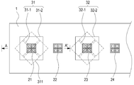
도 4는 본 발명의 일 실시예에 따른 이중대역 이중편파 이동통신 기지국 안테나의 평면도이며, 도 5는 도 4의 A-A'부분 일부 투과 절단면도이다. 도 6은 도 4의 제1방사소자의 급전 구조를 나타낸 평면 및 배면도이며, 도 7은 도 6의 사시도로서, 도 6 및 도 7에서는 설명의 편의를 위해 제1방사소자들 슬롯 구조 및 급전용 도체 패턴이 형성된 회로기판을 나타내었으며, 그 외의 구성에 대해서는 생략하였다.FIG. 4 is a plan view of a dual-band dual polarization mobile communication base station antenna according to an embodiment of the present invention, and FIG. 5 is a cross-sectional view taken along the line A-A 'in FIG. FIG. 6 is a plan view and a rear view showing the feeding structure of the first radiating element of FIG. 4, FIG. 7 is a perspective view of FIG. 6, A circuit board on which a dedicated conductor pattern is formed is shown, and other configurations are omitted.
도 4 내지 도 7을 참조하면, 본 발명의 일 실시예에 따른 안테나는 제1주파수 대역(예를 들어, 700/800MHz 대역)의 일명, 슬롯 타입 제1방사소자들(31, 32)이 반사판(1) 상면에 일정 간격으로 배치되어 있다. 또한, 제2주파수 대역(예를 들어, 2GHz 대역)의 다이폴 타입 제2방사소자들(21, 22, 23, 24)들은 상기 제1방사소자들(31, 32)에 적층되거나 또는 제1방사소자들(31, 32) 사이에서 반사판(1) 상면에 직접 설치된다. 4 to 7, an antenna according to an embodiment of the present invention includes a slot type first radiating
제1방사소자들(31, 32) 각각은 본 발명의 특징에 따라 반사판(1) 자체에 전체적으로 X자의 구멍 형태로 직접적으로 형성되어, 서로 직교하는 X자 형태의 이중편파의 송신 신호를 발생하기 위한 슬롯 구조(31-1)와, 슬롯 구조(31-1)의 상면에서 설치되는 알루미늄(은 도금) 또는 구리(은 도금)와 같은 금속 재질의 패치 판(31-2, 32-2)으로 구성된다. 패치 판(31-2. 32-2)은 슬롯 구조(31-1)의 방사 특성을 최적화를 위해 적절한 형태 및 사이즈를 가지며, 하부의 반사판(1)과 절연되게 플라스틱 소재 등의 지지대를 이용하여 설치된다. 즉, 본 발명에서는 반사판(1) 자체가 슬롯 구조를 형성하는 금속 판의 역할을 하게 된다.Each of the first
슬롯 구조(31-1)는 반사판(1)의 뒷면에 부착되는 회로 기판(311)에 미리 적절한 도체 패턴으로 형성되는 급전용 스트립 선로(도 6의 3111)와 커플링 방식으로 송신 신호를 제공받는다. 상기 회로 기판(311)은 통상적인 PCB 기판 형태로 형성될 수 있다.The slot structure 31-1 is provided with a transmission signal in a coupling manner with a feeder strip line (3111 in Fig. 6) previously formed in a suitable conductor pattern on a
X자 형태의 슬롯 구조(31-1)에서 X자 형태의 이중편파 중 일 편파를 각각 발생하는 '/'자 또는 '\'자 슬롯들은 각각 해당 제1주파수 대역(AWS 대역)의 주파수 파장을 고려하여, 예를 들어 2/λ에 대응되게 그 길이가 형성될 수 있다. 이 경우에 각각의 슬롯의 길이는 예를 들어, 약 160mm, 각각의 슬롯의 폭은 예를 들어, 약 2mm로 설계될 수 있다.The '/' or '\' slots that respectively generate one polarized wave of the X-shaped dual polarized wave in the X-shaped slot structure (31-1) are the frequency waves of the corresponding first frequency band (AWS band) , The length may be formed corresponding to 2 /?, For example. In this case, the length of each slot may be designed, for example, to be about 160 mm, and the width of each slot to be, for example, about 2 mm.
X자 형태로 형성되는 이중편파에서 각각의 편파를 발생하는 스트립 선로(3111)를 회로기판(311)에 형성할 경우에, 서로 교차하게(그러나 전기적으로 연결되지 않게) 도체 패턴들을 형성하여야 할 부위가 있는데, 도 6의 (b)에서 A부분에 그 측면 구조를 확대하여 도시한 바와 같이, 서로 교차하는 부위에 도체 패턴들 중 한 도체 패턴을 에어 브리지 구조로 형성한다.When a
한편, 이와 같이, 형성되는 제1방사소자들(31, 32)에 적층되는 제2방사소자들(21, 22)은 제1방사소자들(31, 32)의 패치 판(31-2, 32-2) 상에 설치되며, 패치 판(31-2, 32-2)을 접지단으로 사용하게 된다. 즉, 제2방사소자(21, 22)는 패치 판(31-2, 32-2)에 의해 접지된다. 제1방사소자들(31, 32)에 적층되는 제2방사소자들(21, 22)은 제1방사소자들(31, 32)의 패치 판(31-2, 32-2) 및 반사판(1)을 관통하는 급전 케이블(212)을 통해서 급전망과 연결된다.The second
상기와 같은 구조에 따라, 본 발명에 따른 안테나에서 회로 기판(311)의 급전용 스트립 선로(3111)에 인가되는 송신 신호는 회로 기판(311) 자체의 유전층을 거쳐 슬롯 구조(31-1)에 커플링되며, 이에 따라 슬롯 구조(31-1)에는 송신 신호의 전기장(E field)이 형성된다. 슬롯 구조(31-1)에 형성되는 송신 신호의 전기장은 이후, 적정한 간격을 두고 이격되게 고정된 패치 판(31-2, 32-2)을 거쳐 방사된다.The transmission signal applied to the
상기한 구조를 가지는 본 발명에 따른 제1, 제2방사소자의 적층 배치 방식에서는, 종래의 상부 및 하부 패치 판을 가지는 구조와 비교하여, 패치 판을 하나만 구비하므로, 제1방사소자에 적층되어 설치되는 제2방사소자와, 단독으로 설치되는 제2방사소자들이 높이 차이가 줄어들게 된다. 예를 들어, 본 발명에서 제1방사소자에 적층되어 설치되는 제2방사소자와, 단독으로 설치되는 제2방사소자들 간의 높이 차이는 약 25mm일 수 있다. 이와 같이, 높이 차이가 줄어들게 되므로, 높이 차이를 가지는 제2방사소자들 간에 의해 발생되는 위상 지연(phase delay)이 종래와 비교하여 줄어들게 되며, 안테나 다운 틸트시 수평 빔폭 감소량이 줄어들게 된다.In the lamination arrangement method of the first and second radiating elements according to the present invention having the above-described structure, since only one patch plate is provided as compared with the conventional structure having the upper and lower patch plates, The height difference between the second radiating element to be installed and the second radiating elements to be installed alone is reduced. For example, in the present invention, the height difference between the second radiating element that is stacked and installed on the first radiating element and the second radiating elements that are installed alone may be about 25 mm. In this way, since the height difference is reduced, the phase delay generated by the second radiating elements having the height difference is reduced compared with the conventional one, and the horizontal beam width reduction amount is reduced at the antenna down-tilt.
또한, 이 경우에, 본 발명에 따른 안테나는 종래와 비교하여 제1방사소자 및 이에 적층되어 설치되는 제2방사소자의 높이가 낮아지게 되므로, 전체적인 안테나의 높이를 줄일 수 있게 되어, 종래와 비교하여 보다 소형, 경량화를 만족시킬 수 있게 된다.In this case, since the height of the first radiating element and the second radiating element stacked on the first radiating element are lowered compared with the conventional antenna, the overall height of the antenna can be reduced, So that it is possible to satisfy a smaller size and a lighter weight.
또한, 제1방사소자에 적층되어 설치되는 제2방사소자는 제1방사소자의 패치 판을 접지단으로 사용하게 되는데, 본 발명에서는 제1방사소자의 패치 판은 슬롯 구조의 부위보다 크게 형성되므로, 종래와 비교하여 큰 사이즈로 설계하는 것이 가능하게 된다. 따라서, 본 발명에 따른 패치 판은 그 위에 적층되는 다이폴 타입의 제2방사소자에서 요구되는 접지 면적을 만족시킬 수 있게 되며, 제2방사소자에서 무선 주파수의 패턴 특성 열화를 방지할 수 있게 된다.Also, the second radiating element which is stacked and installed on the first radiating element uses the patch plate of the first radiating element as a ground terminal. In the present invention, the patch plate of the first radiating element is formed larger than the portion of the slot structure , It becomes possible to design a larger size as compared with the conventional one. Accordingly, the patch plate according to the present invention can satisfy the required ground area in the dipole-type second radiating element stacked thereon, and can prevent deterioration of the pattern characteristic of the radio frequency in the second radiating element.
상기와 같이 본 발명의 일 실시예에 따른 이동통신 기지국 안테나의 구성 및 동작이 이루어질 수 있으며, 한편 상기한 본 발명의 설명에서는 구체적인 실시예에 관해 설명하였으나 여러 가지 변형이 본 발명의 범위를 벗어나지 않고 실시될 수 있다.As described above, the configuration and operation of the mobile communication base station antenna according to the embodiment of the present invention can be performed. While the present invention has been described with respect to the specific embodiments, various modifications may be made without departing from the scope of the present invention .
예를 들어, 상기의 설명에서는 제1방사소자에 적층되게 설치되는 제2방사소자가 다이폴 타입인 것을 예로 들어 설명하였으나, 이외에도 본 발명의 다른 실시예들에서는 제1방사소자에 적층되는 제2방사소자가 통상적인 패치 타입의 구조로 구성할 수도 있다.For example, in the above description, the second radiating element that is stacked on the first radiating element is a dipole type. However, in other embodiments of the present invention, the second radiating element The device may be constructed with a conventional patch type structure.
또한, 상기의 설명에서는 제1방사소자에 제2방사소자가 적층되는 경우를 예로 들어 설명하였으나, 이외에도 본 발명의 다른 실시예들에서는 제2방사소자가 적층되지 않고, 본 발명에 따른 구조를 가지는 제1방사소자들이 별도로 설치되도록 하는 구성도 가능하다.In the above description, the case where the second radiating element is laminated on the first radiating element has been described as an example. However, in other embodiments of the present invention, the second radiating element is not laminated, It is also possible to arrange the first radiation elements to be installed separately.
Claims (4)
반사판과;
상기 반사판 상에 형성되는 제1주파수 대역의 제1방사소자를 포함하며;
상기 제1방사소자는
상기 반사판 자체에 전체적으로 X자의 구멍 형태로 직접적으로 형성되어, 서로 직교하는 X자 형태의 이중편파의 송신 신호를 발생하기 위한 슬롯 구조와;
상기 슬롯 구조의 상면에서 상기 반사판과 절연되게 설치되는 금속 재질의 패치 판을 포함함을 특징으로 하는 이동통신 기지국 안테나.
A mobile communication base station antenna,
A reflector;
A first radiating element of a first frequency band formed on the reflector;
The first radiating element
A slot structure directly formed in the reflector itself as an X-shaped hole to generate an X-shaped dual polarized transmission signal orthogonal to each other;
And a patch plate made of a metal material and insulated from the reflection plate on the upper surface of the slot structure.
The mobile communication base station antenna according to claim 1, further comprising a second radiating element of a second frequency band installed in a structure laminated on the first radiating element.
The mobile communication base station antenna according to claim 2, wherein the second radiating element is a dipole type, and the patch plate of the first radiating element is used as a ground terminal.
상기 제1방사소자의 상기 슬롯 구조는 상기 반사판의 뒷면에 부착되는 회로 기판에 형성되는 급전용 스트립 선로와 커플링 방식으로 연결됨을 특징으로 하는 이동통신 기지국 안테나.4. The method according to any one of claims 1 to 3,
Wherein the slot structure of the first radiating element is coupled to a feeder strip line formed on a circuit board attached to a rear surface of the reflector in a coupling manner.
Priority Applications (6)
| Application Number | Priority Date | Filing Date | Title |
|---|---|---|---|
| KR1020120137888A KR20140069968A (en) | 2012-11-30 | 2012-11-30 | Antenna of mobile communication station |
| JP2015545366A JP2015536626A (en) | 2012-11-30 | 2013-11-29 | Mobile communication base station antenna |
| PCT/KR2013/010990 WO2014084655A1 (en) | 2012-11-30 | 2013-11-29 | Antenna for mobile-communication base station |
| EP13859174.8A EP2928020A4 (en) | 2012-11-30 | 2013-11-29 | Antenna for mobile-communication base station |
| CN201380062404.7A CN104798257A (en) | 2012-11-30 | 2013-11-29 | Antenna for mobile-communication base station |
| US14/723,217 US20150263431A1 (en) | 2012-11-30 | 2015-05-27 | Antenna for mobile-communication base station |
Applications Claiming Priority (1)
| Application Number | Priority Date | Filing Date | Title |
|---|---|---|---|
| KR1020120137888A KR20140069968A (en) | 2012-11-30 | 2012-11-30 | Antenna of mobile communication station |
Publications (1)
| Publication Number | Publication Date |
|---|---|
| KR20140069968A true KR20140069968A (en) | 2014-06-10 |
Family
ID=50828199
Family Applications (1)
| Application Number | Title | Priority Date | Filing Date |
|---|---|---|---|
| KR1020120137888A KR20140069968A (en) | 2012-11-30 | 2012-11-30 | Antenna of mobile communication station |
Country Status (6)
| Country | Link |
|---|---|
| US (1) | US20150263431A1 (en) |
| EP (1) | EP2928020A4 (en) |
| JP (1) | JP2015536626A (en) |
| KR (1) | KR20140069968A (en) |
| CN (1) | CN104798257A (en) |
| WO (1) | WO2014084655A1 (en) |
Cited By (5)
| Publication number | Priority date | Publication date | Assignee | Title |
|---|---|---|---|---|
| WO2016076601A1 (en) * | 2014-11-11 | 2016-05-19 | 주식회사 케이엠더블유 | Mobile communication base station antenna |
| KR101712375B1 (en) * | 2015-11-20 | 2017-03-07 | 주식회사 에이스테크놀로지 | Antenna for sticking the ceiling for decreasing beam tilt difference depend on frequency band |
| WO2021101035A1 (en) * | 2019-11-18 | 2021-05-27 | 주식회사 에이스테크놀로지 | Antenna having symmetrical feed circuit for improving antenna pattern |
| WO2022060170A1 (en) * | 2020-09-18 | 2022-03-24 | 삼성전자 주식회사 | Antenna structure and electronic device comprising same |
| US11462832B2 (en) | 2020-09-16 | 2022-10-04 | Samsung Electro-Mechanics Co., Ltd. | Antenna device |
Families Citing this family (14)
| Publication number | Priority date | Publication date | Assignee | Title |
|---|---|---|---|---|
| CN104393422B (en) * | 2014-11-17 | 2018-05-01 | 京信通信系统(中国)有限公司 | Multi-frequency array antenna |
| US11038272B2 (en) * | 2017-05-29 | 2021-06-15 | Huawei Technologies Co., Ltd. | Configurable antenna array with diverse polarizations |
| CN107257018B (en) * | 2017-06-06 | 2018-08-14 | 江苏亨鑫科技有限公司 | Low frequency radiating element and multifrequency antenna with the low frequency radiating element |
| CN107359415B (en) * | 2017-06-08 | 2020-12-15 | 京信通信技术(广州)有限公司 | Multi-frequency antenna |
| CN108539434B (en) * | 2018-04-17 | 2024-08-09 | 昆山恩电开通信设备有限公司 | Ultra-wideband radiation unit |
| US11101565B2 (en) * | 2018-04-26 | 2021-08-24 | Neptune Technology Group Inc. | Low-profile antenna |
| CN110011073A (en) * | 2019-04-01 | 2019-07-12 | 广州杰赛科技股份有限公司 | Multi-port antenna |
| US10797408B1 (en) * | 2019-04-18 | 2020-10-06 | Huawei Technologies Co., Ltd. | Antenna structure and method for manufacturing the same |
| CN110444858B (en) * | 2019-07-29 | 2021-09-07 | 中信科移动通信技术股份有限公司 | Method for improving index, antenna array and base station antenna |
| CN112531356B (en) | 2019-09-18 | 2022-05-03 | 北京小米移动软件有限公司 | Antenna structure and mobile terminal |
| US11431110B2 (en) | 2019-09-30 | 2022-08-30 | Qualcomm Incorporated | Multi-band antenna system |
| CN115836494A (en) * | 2020-05-01 | 2023-03-21 | 舰队空间科技公司 | LEO satellite communication system and method |
| US11843187B2 (en) * | 2021-04-26 | 2023-12-12 | Amazon Technologies, Inc. | Antenna module grounding for phased array antennas |
| CN115249899A (en) * | 2021-04-28 | 2022-10-28 | 康普技术有限责任公司 | Multiband antenna |
Family Cites Families (14)
| Publication number | Priority date | Publication date | Assignee | Title |
|---|---|---|---|---|
| US5872544A (en) * | 1997-02-04 | 1999-02-16 | Gec-Marconi Hazeltine Corporation Electronic Systems Division | Cellular antennas with improved front-to-back performance |
| DE19823750A1 (en) * | 1998-05-27 | 1999-12-09 | Kathrein Werke Kg | Antenna array with several primary radiator modules arranged vertically one above the other |
| SE9802883L (en) * | 1998-08-28 | 2000-02-29 | Ericsson Telefon Ab L M | Antenna device |
| AU1425501A (en) * | 1999-12-01 | 2001-06-12 | Allgon Ab | An antenna assembly and a method of mounting an antenna assembly |
| JP2003046326A (en) * | 2001-08-01 | 2003-02-14 | Denki Kogyo Co Ltd | Polarized wave sharing antenna |
| JP4112456B2 (en) * | 2003-07-29 | 2008-07-02 | 電気興業株式会社 | Polarized antenna device |
| CN2879453Y (en) * | 2005-08-30 | 2007-03-14 | 杨华 | Plate type mobile communication base station antenna |
| KR100944624B1 (en) | 2008-04-18 | 2010-02-26 | 경희대학교 산학협력단 | Glare Tester for sunlight and artificial lighting |
| KR101085887B1 (en) * | 2008-12-22 | 2011-11-23 | 주식회사 케이엠더블유 | Dual-band dual-polarized base station antenna for mobile communication |
| CN101826658B (en) * | 2009-03-03 | 2013-04-17 | 华为技术有限公司 | Reflecting board of base station antenna and base station antenna |
| KR101125180B1 (en) * | 2009-11-17 | 2012-03-19 | 주식회사 케이엠더블유 | Method for installing radiator elements arranged in different planes and antenna thereof |
| JP4866962B2 (en) * | 2010-04-22 | 2012-02-01 | アルプス電気株式会社 | Antenna device |
| KR101144528B1 (en) * | 2010-08-31 | 2012-05-11 | 주식회사 에이스테크놀로지 | A patch antenna synchronous generating linearly polarized wave and circularly polarized wave |
| CN202076403U (en) * | 2011-05-16 | 2011-12-14 | 摩比天线技术(深圳)有限公司 | Double-frequency dual-polarization antenna oscillator of loading filter |
-
2012
- 2012-11-30 KR KR1020120137888A patent/KR20140069968A/en not_active Application Discontinuation
-
2013
- 2013-11-29 CN CN201380062404.7A patent/CN104798257A/en active Pending
- 2013-11-29 WO PCT/KR2013/010990 patent/WO2014084655A1/en active Application Filing
- 2013-11-29 EP EP13859174.8A patent/EP2928020A4/en not_active Withdrawn
- 2013-11-29 JP JP2015545366A patent/JP2015536626A/en not_active Withdrawn
-
2015
- 2015-05-27 US US14/723,217 patent/US20150263431A1/en not_active Abandoned
Cited By (6)
| Publication number | Priority date | Publication date | Assignee | Title |
|---|---|---|---|---|
| WO2016076601A1 (en) * | 2014-11-11 | 2016-05-19 | 주식회사 케이엠더블유 | Mobile communication base station antenna |
| US10622706B2 (en) | 2014-11-11 | 2020-04-14 | Kmw Inc. | Mobile communication base station antenna |
| KR101712375B1 (en) * | 2015-11-20 | 2017-03-07 | 주식회사 에이스테크놀로지 | Antenna for sticking the ceiling for decreasing beam tilt difference depend on frequency band |
| WO2021101035A1 (en) * | 2019-11-18 | 2021-05-27 | 주식회사 에이스테크놀로지 | Antenna having symmetrical feed circuit for improving antenna pattern |
| US11462832B2 (en) | 2020-09-16 | 2022-10-04 | Samsung Electro-Mechanics Co., Ltd. | Antenna device |
| WO2022060170A1 (en) * | 2020-09-18 | 2022-03-24 | 삼성전자 주식회사 | Antenna structure and electronic device comprising same |
Also Published As
| Publication number | Publication date |
|---|---|
| EP2928020A1 (en) | 2015-10-07 |
| US20150263431A1 (en) | 2015-09-17 |
| EP2928020A4 (en) | 2016-07-20 |
| WO2014084655A1 (en) | 2014-06-05 |
| JP2015536626A (en) | 2015-12-21 |
| CN104798257A (en) | 2015-07-22 |
Similar Documents
| Publication | Publication Date | Title |
|---|---|---|
| KR20140069968A (en) | Antenna of mobile communication station | |
| US11777229B2 (en) | Antennas including multi-resonance cross-dipole radiating elements and related radiating elements | |
| CN107210541B (en) | Mobile base station antenna | |
| KR100666113B1 (en) | Internal Multi-Band Antenna with Multiple Layers | |
| US20230114554A1 (en) | Ultra-wide bandwidth low-band radiating elements | |
| EP2504884B1 (en) | Mimo antenna | |
| US20070008236A1 (en) | Compact dual-band antenna system | |
| KR100980774B1 (en) | Internal mimo antenna having isolation aid | |
| KR101750336B1 (en) | Multi Band Base station antenna | |
| US20120062437A1 (en) | Antenna system with planar dipole antennas and electronic apparatus having the same | |
| KR20120138758A (en) | Antennas with novel current distribution and radiation patterns, for enhanced antenna isolation | |
| WO2012102576A2 (en) | Broad-band dual polarization dipole antenna and antenna array | |
| KR20060094603A (en) | Dielectric chip antenna | |
| US12088017B2 (en) | Radiating element, antenna assembly and base station antenna | |
| CN107004954B (en) | Dual-band antenna and antenna system | |
| EP3465823B1 (en) | C-fed antenna formed on multi-layer printed circuit board edge | |
| CN109728413B (en) | Antenna structure and terminal | |
| Hwang et al. | Cavity-backed stacked patch array antenna with dual polarization for mmWave 5G base stations | |
| US20170170555A1 (en) | Decoupled Antennas For Wireless Communication | |
| KR101644445B1 (en) | Base station antenna | |
| KR20110040393A (en) | Pcb type antenna having via hole structure | |
| EP3799203A1 (en) | Radiating elements having parasitic elements for increased isolation and base station antennas including such radiating elements | |
| US10211538B2 (en) | Directional antenna apparatus and methods | |
| US20080094303A1 (en) | Planer inverted-F antenna device | |
| US11611151B2 (en) | Multiband antenna structure |
Legal Events
| Date | Code | Title | Description |
|---|---|---|---|
| E902 | Notification of reason for refusal | ||
| E601 | Decision to refuse application |