JP2015534420A - Full-band amplifier - Google Patents
Full-band amplifier Download PDFInfo
- Publication number
- JP2015534420A JP2015534420A JP2015542025A JP2015542025A JP2015534420A JP 2015534420 A JP2015534420 A JP 2015534420A JP 2015542025 A JP2015542025 A JP 2015542025A JP 2015542025 A JP2015542025 A JP 2015542025A JP 2015534420 A JP2015534420 A JP 2015534420A
- Authority
- JP
- Japan
- Prior art keywords
- band
- coupled
- transistor
- signal
- gain
- Prior art date
- Legal status (The legal status is an assumption and is not a legal conclusion. Google has not performed a legal analysis and makes no representation as to the accuracy of the status listed.)
- Pending
Links
- 230000007850 degeneration Effects 0.000 claims abstract description 28
- 238000000034 method Methods 0.000 claims description 9
- 230000003139 buffering effect Effects 0.000 claims 3
- 238000013461 design Methods 0.000 abstract description 75
- 239000003990 capacitor Substances 0.000 description 25
- 230000005540 biological transmission Effects 0.000 description 8
- 238000010586 diagram Methods 0.000 description 8
- 238000004891 communication Methods 0.000 description 7
- 238000005516 engineering process Methods 0.000 description 7
- 230000008569 process Effects 0.000 description 4
- 230000001413 cellular effect Effects 0.000 description 3
- 230000008878 coupling Effects 0.000 description 3
- 238000010168 coupling process Methods 0.000 description 3
- 238000005859 coupling reaction Methods 0.000 description 3
- 230000006870 function Effects 0.000 description 3
- 229910044991 metal oxide Inorganic materials 0.000 description 3
- 150000004706 metal oxides Chemical class 0.000 description 3
- 239000004065 semiconductor Substances 0.000 description 3
- 229910000577 Silicon-germanium Inorganic materials 0.000 description 2
- 230000002776 aggregation Effects 0.000 description 2
- 238000004220 aggregation Methods 0.000 description 2
- 230000003321 amplification Effects 0.000 description 2
- 239000000835 fiber Substances 0.000 description 2
- 238000009413 insulation Methods 0.000 description 2
- 238000012986 modification Methods 0.000 description 2
- 230000004048 modification Effects 0.000 description 2
- 238000003199 nucleic acid amplification method Methods 0.000 description 2
- 230000003287 optical effect Effects 0.000 description 2
- JBRZTFJDHDCESZ-UHFFFAOYSA-N AsGa Chemical compound [As]#[Ga] JBRZTFJDHDCESZ-UHFFFAOYSA-N 0.000 description 1
- LEVVHYCKPQWKOP-UHFFFAOYSA-N [Si].[Ge] Chemical compound [Si].[Ge] LEVVHYCKPQWKOP-UHFFFAOYSA-N 0.000 description 1
- 230000008859 change Effects 0.000 description 1
- 230000000295 complement effect Effects 0.000 description 1
- 238000004590 computer program Methods 0.000 description 1
- 239000004020 conductor Substances 0.000 description 1
- 239000012212 insulator Substances 0.000 description 1
- 230000007774 longterm Effects 0.000 description 1
- 238000010295 mobile communication Methods 0.000 description 1
- 238000005457 optimization Methods 0.000 description 1
- 230000003071 parasitic effect Effects 0.000 description 1
- 238000012545 processing Methods 0.000 description 1
- 230000001360 synchronised effect Effects 0.000 description 1
- 238000012546 transfer Methods 0.000 description 1
- 238000004804 winding Methods 0.000 description 1
Images


Classifications
-
- H—ELECTRICITY
- H04—ELECTRIC COMMUNICATION TECHNIQUE
- H04W—WIRELESS COMMUNICATION NETWORKS
- H04W88/00—Devices specially adapted for wireless communication networks, e.g. terminals, base stations or access point devices
- H04W88/02—Terminal devices
-
- H—ELECTRICITY
- H03—ELECTRONIC CIRCUITRY
- H03F—AMPLIFIERS
- H03F3/00—Amplifiers with only discharge tubes or only semiconductor devices as amplifying elements
- H03F3/189—High-frequency amplifiers, e.g. radio frequency amplifiers
- H03F3/19—High-frequency amplifiers, e.g. radio frequency amplifiers with semiconductor devices only
- H03F3/193—High-frequency amplifiers, e.g. radio frequency amplifiers with semiconductor devices only with field-effect devices
-
- H—ELECTRICITY
- H03—ELECTRONIC CIRCUITRY
- H03F—AMPLIFIERS
- H03F3/00—Amplifiers with only discharge tubes or only semiconductor devices as amplifying elements
- H03F3/68—Combinations of amplifiers, e.g. multi-channel amplifiers for stereophonics
-
- H—ELECTRICITY
- H04—ELECTRIC COMMUNICATION TECHNIQUE
- H04B—TRANSMISSION
- H04B1/00—Details of transmission systems, not covered by a single one of groups H04B3/00 - H04B13/00; Details of transmission systems not characterised by the medium used for transmission
- H04B1/005—Details of transmission systems, not covered by a single one of groups H04B3/00 - H04B13/00; Details of transmission systems not characterised by the medium used for transmission adapting radio receivers, transmitters andtransceivers for operation on two or more bands, i.e. frequency ranges
- H04B1/0053—Details of transmission systems, not covered by a single one of groups H04B3/00 - H04B13/00; Details of transmission systems not characterised by the medium used for transmission adapting radio receivers, transmitters andtransceivers for operation on two or more bands, i.e. frequency ranges with common antenna for more than one band
Landscapes
- Engineering & Computer Science (AREA)
- Power Engineering (AREA)
- Computer Networks & Wireless Communication (AREA)
- Signal Processing (AREA)
- Amplifiers (AREA)
Abstract
複数の帯域グループをサポートする全帯域増幅器が開示される。典型的な設計では、装置(例えば、ワイヤレスデバイス、集積回路等)は、複数の帯域グループのための複数のカスコードトランジスタおよび少なくとも1つの利得トランジスタを含む。各帯域グループは、複数の帯域をカバーする。(複数を含む)利得トランジスタは、入力無線周波数(RF)信号を受信する。カスコードトランジスタは、(複数を含む)利得トランジスタに結合され、複数の帯域グループのうちの1つのための出力RF信号を供給する。典型的な設計では、(複数を含む)利得トランジスタは、複数の帯域グループのために複数の利得トランジスタを含む。1つの利得トランジスタおよび1つのカスコードトランジスタは、入力RF信号を増幅し、選択された帯域グループのための出力RF信号を供給することが可能にされる。利得トランジスタは、単一のソースデジェネレーションインダクタの異なるタップに、または異なるソースデジェネレーションインダクタに結合されうる。A full-band amplifier that supports multiple band groups is disclosed. In a typical design, an apparatus (eg, wireless device, integrated circuit, etc.) includes a plurality of cascode transistors and at least one gain transistor for a plurality of band groups. Each band group covers a plurality of bands. The gain transistor (s) receive an input radio frequency (RF) signal. The cascode transistor is coupled to the gain transistor (s) and provides an output RF signal for one of the plurality of band groups. In a typical design, the gain transistor (s) includes multiple gain transistors for multiple band groups. One gain transistor and one cascode transistor are enabled to amplify the input RF signal and provide an output RF signal for the selected band group. The gain transistors can be coupled to different taps of a single source degeneration inductor or to different source degeneration inductors.
Description
[0001] 本開示は、一般に、エレクトロニクスに関し、より具体的には、増幅器に関する。 [0001] The present disclosure relates generally to electronics, and more specifically to amplifiers.
[0002] ワイヤレス通信システムにおけるワイヤレスデバイス(例えば、セルラ電話またはスマートフォン)は、双方向通信のためにデータを送信および受信しうる。ワイヤレスデバイスは、データ送信用の送信機と、データ受信用の受信機とを含みうる。データ送信の場合、送信機は、変調されたRF信号を取得するために、無線周波数(RF)キャリア信号をデータで変調し、適正な出力電力レベルを有する増幅されたRF信号を取得するために、変調されたRF信号を増幅し、アンテナを介して増幅されたRF信号を基地局に送信しうる。データ受信のために、受信機は、アンテナを介して受信されたRF信号を取得することがあり、基地局によって送られたデータを復元するために、受信されたRF信号を増幅および処理することがある。 [0002] A wireless device (eg, a cellular phone or a smartphone) in a wireless communication system may transmit and receive data for two-way communication. The wireless device may include a transmitter for data transmission and a receiver for data reception. In the case of data transmission, the transmitter modulates a radio frequency (RF) carrier signal with data to obtain a modulated RF signal and to obtain an amplified RF signal with the proper output power level The modulated RF signal can be amplified, and the amplified RF signal can be transmitted to the base station via the antenna. For data reception, the receiver may obtain the RF signal received via the antenna and amplify and process the received RF signal to recover the data sent by the base station There is.
[0003] ワイヤレスデバイスは、広い周波数範囲にわたって動作をサポートしうる。ワイヤレスデバイスは、多くの(a number of)増幅器を含むことがあり、各増幅器は、ワイヤレスデバイスによってサポートされる広い周波数範囲の一部分にわたって動作するように設計される。できるだけ少ない増幅器で広い周波数範囲にわたって動作をサポートすることが望ましい。 [0003] A wireless device may support operation over a wide frequency range. A wireless device may include a number of amplifiers, and each amplifier is designed to operate over a portion of the wide frequency range supported by the wireless device. It is desirable to support operation over a wide frequency range with as few amplifiers as possible.
[0015] 以下に記載される詳細な説明は、本開示の典型的な設計の説明として意図され、本開示が実現されうる唯一の設計を表すようには意図されない。ここで、「典型的な(exemplary)」という用語は、「例として、事例として、あるいは実例として機能すること」を意味するために、使用される。「典型的な」ものとして、ここで説明するいずれの設計も、他の設計と比較して、必ずしも、好ましいまたは効果的なものと解釈されるべきものではない。詳細な説明は、本開示の典型的な設計の完全な理解を提供することを目的とした特定の詳細を含む。ここで説明される典型的な設計は、これらの特定の詳細なしで実現されうることが当業者に明らかになるであろう。いくつかの事例では、周知の構造およびデバイスが、ここで提示される例示的な設計の新規性を曖昧にすることを避けるために、ブロック図の形式で示される。 [0015] The detailed description set forth below is intended as a description of exemplary designs of the present disclosure and is not intended to represent the only designs in which the present disclosure can be implemented. Here, the term “exemplary” is used to mean “acting as an example, as an example, or as an example”. As "typical", any design described herein is not necessarily to be construed as preferred or effective as compared to other designs. The detailed description includes specific details for the purpose of providing a thorough understanding of the exemplary designs of the present disclosure. It will be apparent to those skilled in the art that the exemplary design described herein can be implemented without these specific details. In some instances, well-known structures and devices are shown in block diagram form in order to avoid obscuring the novelty of the example design presented herein.
[0016] 複数の帯域グループをカバーしている広い周波数範囲をサポートする全帯域増幅器がここに開示される。全帯域増幅器はまた、ユニバーサル増幅器(universal amplifiers)等と称されうる。全帯域増幅器は、ワイヤレス通信デバイスなどの様々なタイプの電子デバイスのために使用されうる。 [0016] An all-band amplifier that supports a wide frequency range covering multiple band groups is disclosed herein. Full-band amplifiers can also be referred to as universal amplifiers and the like. Full-band amplifiers can be used for various types of electronic devices such as wireless communication devices.
[0017] 図1は、ワイヤレス通信システム120と通信するワイヤレスデバイス110を示す。ワイヤレスシステム120は、ロングタームエボリューション(LTE)システム、符号分割多元接続(CDMA)システム、Global System for Mobile Communications(GSM(登録商標))system、無線ローカルエリアネットワーク(WLAN)システム、または他の何らかのワイヤレスシステムでありうる。CDMAシステムは、広帯域CDMA(WCDMA(登録商標))、CDMA 1X、エボリューションデータ最適化(EVDO)、時分割同期CDMA(TD−SCDMA)、または他の何らかのバージョンのCDMAをインプリメントしうる。簡単にするために、図1は、2つの基地局130および132、および1つのシステムコントローラ140を含むワイヤレスシステム120を示す。一般的に、ワイヤレスシステムは、任意の数の基地局と、任意のセットのネットワークエンティティを含みうる。
FIG. 1 shows a
[0018] ワイヤレスデバイス110はまた、ユーザ機器(UE)、移動局、端末、アクセス端末、加入者ユニット、局等と称されうる。ワイヤレスデバイス110は、セルラ電話、スマートフォン、タブレット、ワイヤレスモデム、携帯情報端末(PDA)、ハンドヘルドデバイス、ラップトップコンピュータ、スマートブック、ネットブック、コードレス電話、無線ローカルループ(WLL)局、ブルートゥース(登録商標)デバイス等でありうる。ワイヤレスデバイス110は、ワイヤレスシステム120と通信しうる。ワイヤレスデバイス110はまた、ブロードキャスト局(例えば、ブロードキャスト局134)からの信号、1つまたは複数のグローバルナビゲーション衛星システム(GNSS)における衛星(例えば、衛星150)からの信号等を受信しうる。ワイヤレスデバイス110は、LTE、WCDMA、CDMA 1X、EVDO、TD−SCDMA、GSM、802.11等のようなワイヤレス通信のための1つまたは複数の無線技術をサポートしうる。
[0018] The
[0019] 図2は、ワイヤレスデバイス110によってサポートされうる、3つの典型的な帯域グループを示す。ワイヤレスデバイス110は、1000メガヘルツ(MHz)よりも低い周波数をカバーする低帯域(LB)、1000MHzから2300MHzの周波数をカバーする中間帯域(MB:mid-band)、および/または2300MHzよりも高い周波数をカバーする高帯域(HB)、において動作することが可能でありうる。例えば、図2に示されるように、低帯域は、698から960MHzをカバーすることがあり、中間帯域は、1475から2170MHzをカバーすることがあり、高帯域は、2300から2690MHzおよび3400から3800MHzをカバーすることがある。低帯域、中間帯域、および高帯域は、帯域の3つのグループ(または帯域グループ)を指し、各帯域グループは、多くの周波数帯域(または簡潔に、「帯域」)を含む。各帯域は、200MHzまでカバーしうる。LTEリリース11は、35個の帯域をサポートし、これはLTE/UMTS帯域と称され、3GPP TS36.101において載せられている。
FIG. 2 shows three exemplary band groups that may be supported by the
[0020] 一般的に、任意の数の帯域グループが定義づけられうる。各帯域グループは、周波数の任意の範囲をカバーすることがあり、これは、図2において示された周波数範囲の何れとも整合しないこともあり、することもある。各帯域グループはまた、任意の数の帯域を含みうる。 [0020] In general, any number of band groups may be defined. Each band group may cover any range of frequencies, which may or may not match any of the frequency ranges shown in FIG. Each band group may also include any number of bands.
[0021] 図3は、図1におけるワイヤレスデバイス110の典型的な設計のブロック図を示す。この典型的な設計では、ワイヤレスデバイス110は、1次アンテナ310に結合されたトランシーバ320、2次アンテナ312に結合されたトランシーバ322、およびデータプロセッサ/コントローラ380を含む。トランシーバ320は、複数の周波数帯域、複数の無線技術、キャリアアグリゲーション等をサポートするために、複数(K個)の受信機330paから330pkおよび複数(K個)の送信機350paから350pkを含む。トランシーバ322は、複数の周波数帯域、複数の無線技術、キャリアアグリゲーション、受信ダイバーシチ、複数の送信アンテナから複数の受信アンテナへの多入力多出力(MIMO)送信等をサポートするために、L個の受信機330saから330slおよびL個の送信機350saから350slを含む。
[0021] FIG. 3 shows a block diagram of an exemplary design of
[0022] 図3において示される典型的な設計では、各受信機330は、LNA 340および受信回路342を含む。データ受信のために、アンテナ310は、基地局および/または他の送信局から信号を受信し、受信されたRF信号を供給し、それはアンテナインターフェース(antenna interface)回路324を通してルーティングされ(routed)、選択された受信機に入力RF信号として提示される。アンテナインタ−フェース回路324は、スイッチ、デュプレクサ、送信フィルタ、受信フィルタ、整合回路等を含みうる。以下の説明は、受信機330paが選択された受信機であると仮定する。受信機330pa内で、LNA 340paは、入力RF信号を増幅し、出力RF信号を供給する。受信回路342paは、RFからベースバンドへ出力RF信号をダウンコンバートし、ダウンコンバートされた信号を増幅およびフィルタし、アナログ入力信号をデータプロセッサ380へ供給する。受信回路342paは、ミキサ、フィルタ、増幅器、整合回路、発振器、ローカル発振器(LO)ジェネレータ、位相同期ループ(PLL:phase locked loop)等を含みうる。トランシーバ320および322における各残りの受信機330は、受信機330paと同様の方法で動作しうる。
In the exemplary design shown in FIG. 3, each receiver 330 includes an LNA 340 and a receiving circuit 342. For data reception,
[0023] 図3において示される典型的な設計では、各送信機350は、送信回路352および電力増幅器(PA)354を含む。データ送信のために、データプロセッサ380は、送信されるべきデータを処理(例えば、符号化および変調)し、選択された送信機へアナログ出力信号を供給する。以下の説明は、送信機350paが選択された送信機であると仮定する。送信機350pa内では、送信回路352paが、アナログ出力信号をベースバンドからRFに増幅、フィルタ、およびアップコンバートして、変調されたRF信号を供給する。送信回路352paは、増幅器、フィルタ、ミキサ、整合回路、発振器、LOジェネレータ、PLL等を含みうる。PA 354paは、変調されたRF信号を受信および増幅して、適正な出力電力レベルを有する送信RF信号を供給する。送信RF信号は、アンテナインターフェース回路324を通してルーティングされ、アンテナ310を介して送信される。トランシーバ320および322における各残りの送信機350は、送信機350paと同様の方法で動作しうる。
In the exemplary design shown in FIG. 3, each transmitter 350 includes a transmission circuit 352 and a power amplifier (PA) 354. For data transmission, the
[0024] 図3は、受信機330および送信機350の典型的な設計を示す。受信機および送信機はまた、図3において示されない、フィルタ、整合回路等のような他の回路を含みうる。トランシーバ320および322の全てまたは一部は、1つまたは複数のアナログ集積回路(IC)、RF IC(RFIC)、混合信号IC(mixed-signal ICs)等上でインプリメントされうる。例えば、LNA 340および受信回路342は、1つのモジュール上でインプリメントされることがあり、それはRFIC等でありうる。トランシーバ320および322における回路はまた、他の方法でインプリメントされうる。
FIG. 3 shows an exemplary design of receiver 330 and transmitter 350. The receiver and transmitter may also include other circuits such as filters, matching circuits, etc. not shown in FIG. All or a portion of
[0025] データプロセッサ/コントローラ380は、ワイヤレスデバイス110のための様々な機能を実行しうる。例えば、データプロセッサ380は、受信機330を介して受信されているデータおよび送信機350を介して送信されているデータについて処理を実行しうる。コントローラ380は、トランシーバ320および322内の様々な回路の動作を制御しうる。メモリ382は、データプロセッサ/コントローラ380のためのプログラムコードおよびデータを格納しうる。データプロセッサ/コントローラ380は、1つまたは複数の特定用途向け集積回路(ASIC)および/または他のIC上でインプリメントされうる。
[0025] The data processor /
[0026] ワイヤレスデバイス110は、複数の帯域グループ、複数の無線技術、および/または複数のアンテナをサポートしうる。ワイヤレスデバイス110は、複数の帯域グループ、複数の無線技術、および/または複数のアンテナを介する受信をサポートするために、多くのLNAを含みうる。
[0026] The
[0027] 本開示の態様において、全帯域LNAは、複数の帯域グループを介する受信をサポートするために使用されうる。全帯域LNAは、複数の帯域グループをサポートするLNAであり、(i)全てのサポートされる帯域グループのための単一の入力、および(ii)例えば、各帯域グループのための1つの出力というような、複数の帯域グループのための複数の出力を有する。全帯域LNAは、その入力において入力RF信号を受信することがあり、その複数の出力のうちの1つにおいて出力RF信号を供給することがある。全帯域LNAは、複数の帯域グループをカバーし、同じ帯域グループにおける複数の帯域をカバーするマルチバンドLNAとは異なる。 [0027] In aspects of this disclosure, the full-band LNA may be used to support reception via multiple band groups. An all-band LNA is an LNA that supports multiple band groups: (i) a single input for all supported band groups, and (ii) one output for each band group, for example. Such as having multiple outputs for multiple band groups. A full band LNA may receive an input RF signal at its input and may provide an output RF signal at one of its outputs. The full-band LNA covers a plurality of band groups and is different from a multi-band LNA that covers a plurality of bands in the same band group.
[0028] 全帯域LNAは、様々な回路設計でインプリメントされうる。全帯域LNAのいくつかの典型的な設計が以下に説明される。全帯域LNAはまた、様々なタイプのトランジスタでインプリメントされうる。N型金属酸化膜半導体(NMOS: N-channel metal oxide semiconductor)トランジスタでインプリメントされる全帯域LNAのいくつかの典型的な設計が以下に説明される。 [0028] The full-band LNA may be implemented with various circuit designs. Some typical designs of full-band LNA are described below. A full-band LNA can also be implemented with various types of transistors. Several exemplary designs of full-band LNAs implemented with N-channel metal oxide semiconductor (NMOS) transistors are described below.
[0029] 図4Aは、共有されるソースデジェネレーションインダクタを有する全帯域LNA 440の典型的な設計の概略図を示す。全帯域LNA 440は、図3におけるLNA 340のうちの任意の1つのために使用されうる。図4Aにおいて示される典型的な設計では、全帯域LNA 440は、低帯域、中間帯域、高帯域の3つの帯域グループそれぞれのための3つの増幅回路450a、450bおよび450cを含む。
[0029] FIG. 4A shows a schematic diagram of an exemplary design of full-
[0030] 図4Aにおいて示される典型的な設計では、各増幅回路450は、カスコードトランジスタ456に、また、マルチタップ(multi-tap)ソースデジェネレーションインダクタ452にも結合された利得トランジスタ454を含む。低帯域のための増幅回路450a内で、利得トランジスタ454aは、そのゲートに入力RF信号(RFin)を受信させ、そのソースをマルチタップインダクタ452の一端に結合させる。マルチタップインダクタ452は、4つのタップA、B、CおよびDを有し、タップAおよびDは、インダクタ452の2つの末端に対応する。インダクタ452は、利得トランジスタ454aのソースに結合されたタップAおよび回路接地に結合されたタップDを有する。カスコードトランジスタ456aは、そのソースを利得トランジスタ454aのドレインに結合させ、そのゲートに低帯域のための第1のイネーブル制御信号(enable control signal)(Venb1)を受信させ、そのドレインを増幅回路450aの出力に結合させる。
[0030] In the exemplary design shown in FIG. 4A, each amplifier circuit 450 includes a gain transistor 454 coupled to a cascode transistor 456 and also to a multi-tap
[0031] 中間帯域のための増幅回路450bは、利得トランジスタ454bおよびカスコードトランジスタ456bを含み、それらは低帯域のための増幅回路450aにおけるカスコードトランジスタ456aおよび利得トランジスタ454aと同様の方法で結合される。高帯域のための増幅回路450cは、利得トランジスタ454cおよびカスコードトランジスタ456cを含み、それらもまた、低帯域のための増幅回路450aにおけるカスコードトランジスタ456aおよび利得トランジスタ454aと同様の方法で結合される。中間帯域のための利得トランジスタ454bのソースは、マルチタップインダクタ452のタップBに結合され、高帯域のための利得トランジスタ454cのソースはマルチタップインダクタ452のタップCに結合される。利得トランジスタ454aから454cおよびカスコードトランジスタ456aから456cは、図4Aにおいて示されるようにNMOSトランジスタで、または他のタイプのトランジスタで、インプリメントされうる。
[0031]
[0032] インダクタ452は、3つすべての利得トランジスタ454a、454bおよび454cのためのソースデジェネレーションインダクタとしての役割を果たし、それらは、インダクタ452の異なるタップにおけるそれらの接続のために、徐々に小さくなるソースインダクタンスを観察(observe)する。特に、高帯域のための利得トランジスタ454cは、タップCに結合され、それは回路接地に最も近く、したがって最も小さいソースデジェネレーションインダクタンスを観察する。中間帯域のための利得トランジスタ454bは、より高いタップBに結合され、したがって、より大きなソースデジェネレーションインダクタンスを観察する。低帯域のための利得トランジスタ454aは、タップAにおけるインダクタ452のトップエンド(top end)に結合され、したがって最も大きいソースデジェネレーションインダクタンスを観察する。
[0032]
[0033] 図4Aにおいて示される典型的な設計では、様々なキャパシタ458は、利得トランジスタ454aのソースおよびゲートにわたって存在しうる。キャパシタ458は、利得トランジスタ454a、454bおよび454cの寄生キャパシタンス(parasitic capacitance)を含みうる。キャパシタ458はまた、切り替え可能なキャパシタのバンクを含むことがあり、それは利得トランジスタ454aのソースとゲートとの間で結合されることがあり、全帯域LNA 440の入力インピーダンスを微調整(fine-tune)するために使用されることがある。各切り替え可能なキャパシタは、スイッチと直列に結合されたキャパシタでインプリメントされうる。バンクにおけるキャパシタは、全帯域LNA 440のための優良な入力整合(good input matching)を取得するために選択されうる。
[0033] In the exemplary design shown in FIG. 4A, various capacitors 458 may exist across the source and gate of
[0034] 増幅回路450a、450bおよび450cは、それぞれ3つの負荷回路470a、470bおよび470cに結合される。図4Aにおいて示される典型的な設計では、各負荷回路470は、1次コイル474および2次コイル476を備える変圧器472を含む。コイルはまた、インダクタコイル、巻線(winding)、コンダクタ等とも称されうる。低帯域のための負荷回路470a内では、変圧器472aは(i)増幅回路450aの出力と電源(VDD)との間で結合される1次コイル474aおよび(ii)低帯域のためのダウンコンバータ(図4Aに図示せず)に第1の差動増幅RF信号(RFamp1)を供給する2次コイル476aを含む。中間帯域のための負荷回路470bは、(i)増幅回路450bの出力とVDD電源との間で結合される1次コイル474bおよび(ii)中間帯域のためのダウンコンバータ(図4Aに図示せず)に第2の差動増幅RF信号(RFamp2)を供給する2次コイル476bを有する変圧器472bを含む。高帯域のための負荷回路470cは、(i)増幅回路450cの出力とVDD電源との間で結合される1次コイル474cおよび(ii)高帯域のためのダウンコンバータ(図4Aに図示せず)に第3の差動増幅RF信号(RFamp3)を供給する2次コイル476cを有する変圧器472cを含む。変圧器472a、472bおよび472cは、カスコードトランジスタ456a、456b、および456cそれぞれのドレインに結合される。変圧器472a、472bおよび472cは、低帯域、中間帯域、および高帯域それぞれのために優良なパフォーマンスを提供するように設計されうる。
[0034]
[0035] 1つの典型的な設計では、各負荷回路470は、別個のダウンコンバータに結合されうる。別の典型的な設計では、複数の負荷回路470は、スイッチを介して共有されるダウンコンバータに結合されうる。スイッチは、任意の所与の瞬間において共有されるダウンコンバータに1つの負荷回路から増幅されたRF信号を通過するように制御されうる。両方の典型的な設計のために、各ダウンコンバータは、RFからベースバンドまたは中間周波数(IF:intermediate frequency)の何れかに増幅されたRF信号の直交ダウンコンバージョンを実行するために、2つのミキサを含みうる。 [0035] In one exemplary design, each load circuit 470 may be coupled to a separate downconverter. In another exemplary design, the plurality of load circuits 470 may be coupled to a shared down converter via a switch. The switch can be controlled to pass the amplified RF signal from one load circuit to the shared downconverter at any given moment. For both typical designs, each downconverter has two mixers to perform quadrature downconversion of the RF signal amplified from RF to either baseband or intermediate frequency (IF). Can be included.
[0036] 負荷回路470はまた、他の方法でもインプリメントされうる。別の典型的な設計では、負荷回路は、増幅回路の出力とVDD電源との間で結合される可能性のあるキャパシタおよびインダクタを含みうる。さらに別の典型的な設計では、負荷回路は、そのソースをVDD電源に結合させ、そのドレインをカスコードトランジスタ456のドレインに結合させるP型金属酸化膜半導体(PMOS:P-channel metal oxide semiconductor)トランジスタを含みうる。PMOSトランジスタは、カスコードトランジスタ456のためのアクティブな負荷を提供しうる。 [0036] The load circuit 470 may also be implemented in other ways. In another exemplary design, the load circuit may include a capacitor and an inductor that may be coupled between the output of the amplifier circuit and the VDD power supply. In yet another exemplary design, the load circuit has a P-channel metal oxide semiconductor (PMOS) transistor that has its source coupled to the VDD power supply and its drain coupled to the drain of the cascode transistor 456. Can be included. The PMOS transistor can provide an active load for the cascode transistor 456.
[0037] 増幅回路450a、450bおよび450cは、様々な方法でインプリメントされうる。典型的な設計では、利得トランジスタ454a、454bおよび454cは、同様のトランジスタサイズを有することがあり、カスコードトランジスタ456a、456bおよび456cもまた、同様のトランジスタサイズを有することがある。別の典型的な設計では、利得トランジスタ454a、454bおよび454cは、異なるトランジスタサイズを有することがあり、および/またはカスコードトランジスタ456a、456bおよび456cは、異なるトランジスタサイズを有することがある。典型的な設計では、利得トランジスタ454a、454bおよび454cは、同様のバイアス電流を有することがあり、それは3つすべての帯域グループに優良なパフォーマンスを提供するために選択されることがある。別の典型的な設計では、利得トランジスタ454a、454b、および454cは、異なるバイアス電流を有しうる。各利得トランジスタ454のためのバイアス電流は、関連付けられた帯域グループに優良なパフォーマンスを提供するために選択されうる。
[0037] The
[0038] 図4Aは、3つの帯域グループのための3つの増幅回路450a、450bおよび450cを含む全帯域LNA 440を示す。全帯域LNAは、より少ないまたはより多い帯域グループのための3つよりも少ないまたは多い増幅回路450を含みうる。
[0038] FIG. 4A shows a full-
[0039] 全帯域LNA 440は、入力RF信号を受信し、それは3つすべての増幅回路450a、450bおよび450cに適用される。入力RF信号は、対象の帯域グループ、すなわち、選択された帯域グループにおける1つまたは複数の帯域における1つまたは複数の送信を含みうる。選択された帯域グループのための増幅回路450は、入力RF信号を増幅し、選択された帯域グループのための出力RF信号を供給することが可能にされうる。選択された帯域グループのための負荷回路470は、イネーブルされた増幅回路450から出力RF信号を受信し、選択された帯域グループのための増幅されたRF信号を供給しうる。他の帯域グループのための残りの増幅回路450は、ディスエーブル(disabled)されうる。
[0039] The full-
[0040] 図4Bは、低帯域が選択される場合の全帯域LNA 440の動作を示す。この場合において、増幅回路450aは、カスコードトランジスタ456aのゲートにおいてVenb1信号上で適切なバイアス電圧を提供することによって低帯域のための第1の出力RF信号(RFout1)を生成することがイネーブルされる。負荷回路470aは、RFout1信号を受信し、低帯域のためにダウンコンバータへRFamp1信号を供給する。利得トランジスタ454aは、全体のインダクタ452を介して大きいソースデジェネレーションインダクタンスを観察する。増幅回路450bおよび450cは、カスコードトランジスタ456bおよび456cそれぞれのゲートにおいてVenb2およびVenb3信号上で低い電圧を供給することによってディスエーブルされる。
[0040] FIG. 4B shows the operation of the full-
[0041] 図4Cは、中間帯域が選択される場合の全帯域LNA 440の動作を示す。この場合において、増幅回路450bは、カスコードトランジスタ456bのゲートにおいてVenb2信号上で適切なバイアス電圧を供給することによって中間帯域のための第2の出力RF信号(RFout2)を生成することがイネーブルされる。負荷回路470bは、RFout2信号を受信し、中間帯域のためにダウンコンバータへRFamp2信号を供給する。利得トランジスタ454bは、タップBから回路接地へインダクタ452の一部を介して中間の(medium)ソースデジェネレーションインダクタンスを観察する。増幅回路450aおよび450cは、カスコードトランジスタ456aおよび456cそれぞれのゲートにおいてVenb1およびVenb3信号上で低い電圧を供給することによってディスエーブルされる。
[0041] FIG. 4C shows the operation of the full-
[0042] 図4Dは、高帯域が選択される場合の全帯域LNA 440の動作を示す。この場合において、増幅回路450cは、カスコードトランジスタ456cのゲートにおいてVenb3信号上で適切なバイアス電圧を供給することによって高帯域のための第3の出力RF信号(RFout3)を生成することがイネーブルされる。負荷回路470cは、RFout3信号を受信し、高帯域のためにダウンコンバータへRFamp3信号を供給する。利得トランジスタ454cは、タップCから回路接地へインダクタ452の一部を介して小さい(small)ソースデジェネレーションインダクタンスを観察する。増幅回路450aおよび450bは、カスコードトランジスタ456aおよび456bそれぞれのゲートにおいてVenb1およびVenb2信号上で低い電圧を供給することによってディスエーブルされる。
[0042] FIG. 4D shows the operation of the full-
[0043] 典型的な設計では、増幅回路における利得トランジスタは、(i)増幅回路がイネーブルされるときの飽和領域(saturation region)または(ii)増幅回路がディスエーブルされるときの線形領域(linear region)において動作しうる。増幅回路がディスエーブルされるときの線形領域における利得トランジスタを動作することは、増幅回路または帯域グループのどちらが選択されるかに関わらず、全帯域LNA 440の入力インピーダンスにおける変化を減少させうる。利得トランジスタの入力キャパシタンス(CIN)は、

のように表される。ここで、Wは幅を示し、Lは利得トランジスタの長さを示し、COXは利得トランジスタのゲート酸化キャパシタンス(oxide capacitance)を示す。 It is expressed as Here, W represents the width, L represents the length of the gain transistor, and C OX represents the gate oxide capacitance of the gain transistor.
[0044] 式(1)および式(2)において示されるように、増幅回路がイネーブルであるかディスエーブルであるかに依存して利得トランジスタの入力インピーダンスにおける有限の(finite)変化がありうる。しかしながら、全帯域LNA 440の入力インピーダンスは、どの増幅回路が選択されるかに関わらず、および、たとえ(even)利得トランジスタの入力インピーダンスにおける変化を伴なって(with)も、許容範囲の制限内で維持されうる。許容範囲の制限内で全帯域LNA 440の入力インピーダンスを維持することは、全ての帯域グループのためのインピーダンス整合および/または電力を改良(improve)しうる。
[0044] As shown in equations (1) and (2), there may be a finite change in the input impedance of the gain transistor depending on whether the amplifier circuit is enabled or disabled. However, the input impedance of the full-
[0045] 図5は、別個のソースデジェネレーションインダクタを有する全帯域LNA 540の典型的な設計の概略図を示す。全帯域LNA 540はまた、図3におけるLNA 340のうちの任意の1つのために使用されうる。図5において示される典型的な設計では、全帯域LNA 540は、低帯域、中間帯域、および高帯域それぞれのために3つの増幅回路550a、550bおよび550cを含む。各増幅回路550は、カスコードトランジスタ556に、また、ソースデジェネレーションインダクタ552にも結合される利得トランジスタ554を含む。低帯域のための増幅回路550a内で、利得トランジスタ554aは、そのゲートに入力RF信号を受信させ、そのソースをインダクタ552aの一端に結合させる。インダクタ552aのもう一端は、回路接地に結合される。カスコードトランジスタ556aは、そのソースを利得トランジスタ554aのドレインに結合させ、そのゲートに低帯域のための第1のイネーブル制御信号(Venb1)を受信させ、そのドレインを増幅回路550aの出力に結合させる。
[0045] FIG. 5 shows a schematic diagram of an exemplary design of a full-
[0046] 中間帯域のための増幅回路550bは、利得トランジスタ554b、カスコードトランジスタ556b、およびインダクタ552bを含み、それらは低帯域のための増幅回路550aにおけるインダクタ552a、カスコードトランジスタ556a、および利得トランジスタ554aと同様の方法で結合される。高帯域のための増幅回路550cは、利得トランジスタ554c、カスコードトランジスタ556c、およびインダクタ552cを含み、それらは低帯域のための増幅回路550aにおけるインダクタ552a、カスコードトランジスタ556a、および利得トランジスタ554aと同様の方法で結合される。インダクタ552a、552bおよび552cは、低帯域、中間帯域、および高帯域それぞれのために優良なパフォーマンスを提供するように設計されうる。カスコードトランジスタ556a、556b、および556cのドレインは、それぞれ負荷回路570a、570bおよび570cに結合され、(例えば、図4Aに示されるような)変圧器および/または他の回路を備えうる。負荷回路570a、570bおよび570cは、低帯域、中間帯域、および高帯域それぞれのために優良なパフォーマンスを提供するように設計されうる。
[0046] Amplifier circuit 550b for the intermediate band includes
[0047] 図6は、ソースデジェネレーションインダクタを有さない全帯域LNA 640の典型的な設計の概略図を示す。全帯域LNA 640はまた、図3におけるLNA 340のうちの任意の1つのために使用されうる。図6において示される典型的な設計では、全帯域LNA 640は、低帯域、中間帯域、および高帯域それぞれのために3つのカスコードトランジスタ656a、656b、および656cと共通(common)利得トランジスタ654を含む。利得トランジスタ654は、そのゲートに入力RF信号(RFin)を受信させ、そのソースを回路接地に結合させる。カスコードトランジスタ656aは、そのソースを利得トランジスタ654のドレインに結合させ、そのゲートに低帯域のための第1のイネーブル制御信号(Venb1)を受信させ、そのドレインを低帯域のための負荷回路670aに結合させる。カスコードトランジスタ656bは、そのソースを利得トランジスタ654のドレインに結合させ、そのゲートに中間帯域のための第2のイネーブル制御信号(Venb2)を受信させ、そのドレインを中間帯域のための負荷回路670bに結合させる。カスコードトランジスタ656cは、そのソースを利得トランジスタ654のドレインに結合させ、そのゲートに高帯域のための第3のイネーブル制御信号(Venb3)を受信させ、そのドレインを高帯域のための負荷回路670cに結合させる。負荷回路670a、670bおよび670cは、(図4Aに示されるような)変圧器および/または他の回路を備えうる。負荷回路670a、670bおよび670cは、低帯域、中間帯域、および高帯域それぞれのために優良なパフォーマンスを提供するように設計されうる。
[0047] FIG. 6 shows a schematic diagram of an exemplary design of a full-
[0048] 図7は、共有されるソースデジェネレーションインダクタおよびフィードバックを有する全帯域LNA 442の典型的な設計の概略図を示す。全帯域LNA 442はまた、図3におけるLNA 340のうちの任意の1つのためにも使用されうる。図7において示される典型的な設計では、図4Aのために上記で説明されるように、全帯域LNA 442は、低帯域、中間帯域、および高帯域それぞれのために3つの増幅回路450a、450bおよび450cを含む。全帯域LNA 442はさらに、カスコードトランジスタ456a、456bおよび456cのドレインと利得トランジスタ454a、454bおよび454cのゲートとの間、すなわち、増幅回路450a、450bおよび450cの共通入力および出力との間で結合されたフィードバック回路460を含む。
[0048] FIG. 7 shows a schematic diagram of an exemplary design of full-
[0049] 図7において示される典型的な設計では、フィードバック回路460は、スイッチ462a、462b、および462c、レジスタ464、およびキャパシタ466を含む。レジスタ464およびキャパシタ466は、直列に結合され、キャパシタ466の下部端末(bottom terminal)は利得トランジスタ454a、454bおよび454cのゲートに結合される。スイッチ462a、462b、および462cは、1つの端末をレジスタ464に結合させ、もう1つの端末をカスコードトランジスタ456a、456bおよび456cそれぞれのドレインに結合させる。スイッチ462a、462b、および462cは、それぞれフィードバック回路460をその関連付けられたカスコードトランジスタ456へ接続するためにクローズ(closed)されることがあり、フィードバック回路460を関連付けられたカスコードトランジスタ456から切断する(disconnect)ために開かれる(opened)ことがある。フィードバック回路460はまた、トランジスタのような1つまたは複数のアクティブな回路を含みうる。
[0049] In the exemplary design shown in FIG. 7,
[0050] 典型的な設計では、フィードバック回路460は、入力電力整合(match)を提供するために低帯域のためにイネーブルされおよび使用されうる。中間帯域および高帯域のために、フィードバック回路460はディスエーブルされることがあり、ソースデジェネレーションインダクタ452は入力電力整合のために使用されうる。フィードバック回路460はまた、他の方法で使用されうる。
[0050] In a typical design,
[0051] フィードバック回路460は、全帯域LNA 442のための入力整合を支援しうる。フィードバック回路460はまた、増幅回路450a、450bおよび/または450cの線形性(linearity)を改良しうる。各増幅回路450は、(i)関連付けられたスイッチ462がクローズされている場合、フィードバック回路460およびソースデジェネレーションインダクタ452の両方または(ii)関連付けられたスイッチ462が開いている場合、ソースデジェネレーションインダクタ452のみによって線形にされ(linearized)うる。フィードバック回路460で改良された線形性(The improved linearity with feedback circuit 460)は、より小さいインダクタ452に、所望の線形性を取得するために使用されることを可能にしうる。
[0051] The
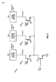
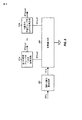
[0052] 図8は、調節可能な整合回路830を有する全帯域LNA 840の典型的な設計の概略図を示す。全帯域LNA 840は、上記で説明された全帯域LNAの設計のうちの任意のものに基づいてインプリメントされうる。全帯域LNA 840は、入力RF信号(RFin)を受信する入力とK個の帯域グループのために出力RF信号(RFout1からRFoutK)を供給するK個の出力を含み、ここで、Kは1より大きい任意の整数値でありうる。調節可能な整合回路830は、全帯域LNA 840の入力に結合され、LNA 840のための入力整合を実行する。整合回路830は、受信されたRF信号(RFrx)を受信し、全帯域LNA 840へ入力RF信号を供給する。K個の負荷回路870aから870kは、全帯域LNA 840のK個の出力に結合され、K個の帯域グループのために設計される。各負荷回路870は、(例えば、図4Aに示されるような)変圧器および/または他の回路要素を備えうる。
[0052] FIG. 8 shows a schematic diagram of an exemplary design of full-
[0053] 調節可能な整合回路830は、様々な方法でインプリメントされうる。調節可能な整合回路830のいくつかの典型的な設計が以下に説明される。
[0053] The
[0054] 図9Aは、Lトポロジ(L topology)に基づいて調節可能な整合回路830aの典型的な設計を示す。Lトポロジは、シャント回路要素に結合された直列回路要素を含む。直列回路要素は、2つのノード間で接続された回路要素である。シャント回路要素は、ノードと回路接地との間で接続された回路要素である。回路要素は、インダクタ、キャパシタ、レジスタ等でありうる。整合回路830aは、(i)整合回路830aの入力と出力との間で結合された直列インダクタ912および(ii)整合回路830aの出力と回路接地との間で結合された調節可能なシャントキャパシタ914を含む。
[0054] FIG. 9A shows an exemplary design of a
[0055] 図9Bは、Lトポロジに基づいて調節可能な整合回路830bの典型的な設計を示す。整合回路830bは、(i)整合回路830bの入力と出力との間に結合された調節可能な直列キャパシタ922、(ii)整合回路830bの出力と回路接地との間で結合されたシャントインダクタ924を含む。
[0055] FIG. 9B shows an exemplary design of a
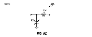
[0056] 図9Cは、Rトポロジ(R topology)に基づいて調節可能な整合回路830cの典型的な設計を示す。Rトポロジは、直列回路要素に結合されたシャント回路要素を含む。整合回路830cは、(i)整合回路830cの入力と回路接地との間に結合された調節可能なシャントキャパシタ932および(ii)整合回路830cの入力と出力との間で結合された直列インダクタ934を含む。
[0056] FIG. 9C shows an exemplary design of a
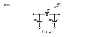
[0057] 図9Dは、Piトポロジ(Pi topology)に基づいて調節可能な整合回路830dの典型的な設計を示す。Piトポロジは、直列回路要素に結合されたシャント回路要素を含み、これは、別のシャント回路要素に結合される。整合回路830dは、(i)整合回路830dの入力と回路接地との間で結合されたシャントキャパシタ942、(ii)整合回路830dの入力と出力との間で結合される直列インダクタ944、および(iii)整合回路830dの出力と回路接地との間で結合される調節可能なシャントキャパシタ946を含む。
[0057] FIG. 9D shows an exemplary design of matching
[0058] 図9Eは、2つのRセクションを有する調節可能な整合回路830eの典型的な設計を示す。整合回路830eは、(i)整合回路830eの入力とVDD電源との間で結合されるシャントインダクタ952、(ii)整合回路830eの入力とノードEとの間で結合される直列キャパシタ954、(iii)ノードEと回路接地との間で結合される調節可能なシャントキャパシタ956、および(iv)整合回路830eの出力とノードEとの間で結合される直列インダクタ958を含む。
[0058] FIG. 9E shows an exemplary design of an adjustable matching circuit 830e having two R sections. Matching circuit 830e includes (i) a
[0059] 図9Fは、Piトポロジに基づいて調節可能な整合回路830fの典型的な設計を示す。整合回路830fは、(i)整合回路830fの入力とVDD電源との間で結合されたシャントインダクタ962、(ii)整合回路830fの入力と出力との間で結合される直列キャパシタ964、(iii)整合回路830fの出力と回路接地との間で結合される調節可能なシャントキャパシタ966、および(iv)整合回路830fの出力と回路接地との間で結合されるシャントインダクタ968を含む。
[0059] FIG. 9F shows an exemplary design of a
[0060] 固定された(fixed)整合回路はまた、図9Aから9Fにおいて示される典型的な設計のうちの任意のものに基づいてインプリメントされうる。この場合において、各調整可能な回路要素(例えば、各調整可能なキャパシタ)は、固定された回路要素(例えば、固定されたキャパシタ)と置き換えられうる。 [0060] A fixed matching circuit may also be implemented based on any of the exemplary designs shown in FIGS. 9A-9F. In this case, each adjustable circuit element (eg, each adjustable capacitor) can be replaced with a fixed circuit element (eg, a fixed capacitor).
[0061] 異なる帯域グループのための変圧器は、様々な方法でインプリメントされうる。変圧器の1次および2次コイルは、所望のインダクタンスおよびカップリング(coupling)を取得するために、様々なパターンでインプリメントされうる。1次および2次コイルはまた、1つまたは複数の伝導レイヤ(conductive layers)上に組み立てられうる。 [0061] Transformers for different band groups may be implemented in various ways. The primary and secondary coils of the transformer can be implemented in various patterns to obtain the desired inductance and coupling. Primary and secondary coils can also be assembled on one or more conductive layers.
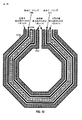
[0062] 図10は、3つの帯域グループのための3つの変圧器の典型的な設計の上面図を示す。3つの変圧器は、図4Aにおける変圧器472aから472c、図5における負荷回路570aから570c、図6における負荷回路670aから670c、図8における負荷回路870aから870cのために使用されうる。
[0062] FIG. 10 shows a top view of an exemplary design of three transformers for three band groups. Three transformers may be used for
[0063] 図10において示される典型的な設計では、低帯域のための変圧器は、第1の伝導レイヤ上の渦巻きパターン(spiral pattern)で形成された1次コイル1074aを含む。中間帯域のための変圧器は、第1の伝導レイヤ上の1次コイル1074aの内部に渦巻きパターンで形成された1次コイル1074bを含む。高帯域のための変圧器は、第1の伝導レイヤ上の1次コイル1074bの内部に渦巻きパターンで形成された1次コイル1074cを含む。接地ガードリング(ground guard ring)1080は、1次コイル1074aと1074bとの間に位置し、これら2つの1次コイル間で絶縁を提供する。接地ガードリング1082は、これらの1次コイル1074bと1074cとの間に位置し、これらの1次コイル間で絶縁を提供する。
[0063] In the exemplary design shown in FIG. 10, the transformer for the low band includes a
[0064] 典型的な設計では、3つの変圧器のための2次コイルは、第2の伝導レイヤ上に渦巻きパターンで配置されうる。各変圧器1072のための2次コイルは、その変圧器についての1次コイルの下に(underneath)直接形成されうる。 [0064] In a typical design, secondary coils for the three transformers may be arranged in a spiral pattern on the second conductive layer. The secondary coil for each transformer 1072 can be directly formed underneath the primary coil for that transformer.
[0065] 図10は、3つの帯域グループのための3つの変圧器についての3つの1次コイル1074a、1074bおよび1074cが互いの内側に形成される典型的な設計を示し、それはスペースを節約しうる。一般に、異なる帯域グループについての変圧器の1次および2次コイルは、任意のレイアウト、任意のパターン、および任意の数のターンでインプリメントされうる。ターンの数、ターンの直径、各コイルの幅および高さ、各変圧器についての1次と2次コイルとの間の間隔、および/または2つのコイルの他の特性(attributes)は、コイル間の所望の結合係数(coupling coefficient)および各コイルのための品質ファクタ(Q)および所望のインダクタンスを取得するために選択されうる。カップリング係数は、コイル間の距離および/またはコイルの配置(placement)を制御することによって変化しうる。
[0065] FIG. 10 shows a typical design in which three
[0066] 図10におけるスタックされた(stacked)トポロジは、変圧器がより小さいエリアにおいて組み立てられることを可能にし、また、差別設計のための2次コイルの2つの末端部の間のより良い整合をもたらしうる。変圧器はまた、並んでいる(side-by-side)トポロジまたは他のトポロジでインプリメントされうる。一般に、異なるトポロジ、レイアウトパターン、および組み立て技法は、変圧器に異なる利点を提供しうる。 [0066] The stacked topology in FIG. 10 allows the transformer to be assembled in a smaller area, and also better matches between the two ends of the secondary coil for differential design Can bring The transformer may also be implemented in a side-by-side topology or other topologies. In general, different topologies, layout patterns, and assembly techniques may provide different advantages for the transformer.
[0067] ここで説明される全帯域増幅器(例えば、LNA)は、様々な利点を提供しうる。第一に、全帯域増幅器は、複数の帯域グループをカバーしている広い周波数範囲をサポートすることができ、それは異なる帯域グループにおける多くの帯域をサポートするために要求される新しいワイヤレスデバイスのために極めて望ましい(highly desirable)ことがある。第二に、全帯域増幅器は、すべてのサポートされる帯域グループのために、例えば、各帯域グループのためのソースデジェネレーションおよび変圧器の使用を介して、優良なパフォーマンスを有しうる。第三に、全帯域増幅器は、単一の入力/出力(I/O)ピンが複数の帯域グループをサポートするために入力RF信号を供給することができるため、ICチップ上のI/Oピンの数を低減させうる。第四に、全帯域増幅器は、各I/Oピンが任意の帯域グループをサポートするように構成されることができるため、より多くの柔軟性を提供しうる。例えば、ICは、20個の全帯域LNAを含むことがあり、(i)20個の低帯域受信機、または(ii)10個の低帯域受信器、5個の中間帯域受信機、および5個の高帯域受信機、または(iii)10個の中間帯域受信機および10個の高帯域受信機、または(iv)受信器の他の何らかの組合せをサポートするように構成されることがある。全帯域増幅器は、他の利点を有しうる。 [0067] The full-band amplifier (eg, LNA) described herein may provide various advantages. First, full-band amplifiers can support a wide frequency range covering multiple band groups, for new wireless devices that are required to support many bands in different band groups It may be highly desirable. Second, the full band amplifier may have good performance for all supported band groups, for example through the use of source degeneration and transformers for each band group. Third, full-band amplifiers can provide I / O pins on an IC chip because a single input / output (I / O) pin can provide input RF signals to support multiple band groups. Can be reduced. Fourth, full-band amplifiers can provide more flexibility because each I / O pin can be configured to support any band group. For example, an IC may include 20 full-band LNAs, (i) 20 low-band receivers, or (ii) 10 low-band receivers, 5 mid-band receivers, and 5 May be configured to support (iii) 10 midband receivers and 10 highband receivers, or (iv) some other combination of receivers. Full-band amplifiers can have other advantages.
[0068] 典型的な設計では、装置(例えば、ワイヤレスデバイス、IC、回路モジュール等)は、複数の帯域グループのための複数のカスコードトランジスタおよび少なくとも1つの利得トランジスタを含みうる。少なくとも1つの利得トランジスタ(例えば、図4Aにおける利得トランジスタ454)は、入力RF信号を受信することがあり、共に結合された(複数を含む)入力を有することがある。複数のカスコードトランジスタ(例えば、カスコードトランジスタ456)は、少なくとも1つの利得トランジスタに結合されることがあり、複数の帯域グループのうちの1つについての出力RF信号を供給することがある。複数の帯域グループは、低帯域、中間帯域、および/または高帯域を含みうる。各帯域グループは、複数の帯域をカバーしうる。 [0068] In a typical design, an apparatus (eg, wireless device, IC, circuit module, etc.) may include a plurality of cascode transistors and at least one gain transistor for a plurality of band groups. At least one gain transistor (eg, gain transistor 454 in FIG. 4A) may receive an input RF signal and may have input (s) coupled together. A plurality of cascode transistors (eg, cascode transistor 456) may be coupled to at least one gain transistor and may provide an output RF signal for one of the plurality of band groups. The plurality of band groups may include a low band, an intermediate band, and / or a high band. Each band group can cover multiple bands.
[0069] 図4Aにおいて示される典型的な設計では、少なくとも1つの利得トランジスタは、複数の帯域グループのための複数の利得トランジスタ(例えば、利得トランジスタ454)を備えうる。複数の利得トランジスタのうちの1つおよび複数のカスコードトランジスタのうちの1つは、入力RF信号を増幅し、選択された帯域グループのための出力RF信号を供給することが可能にされうる。典型的な設計では、複数の利得トランジスタは、異なるトランジスタのサイズおよび/または異なるバイアス電流を有しうる。典型的な設計では、装置は、複数の利得トランジスタおよび回路接地に結合された複数のタップを有するインダクタ(例えば、図4Aにおけるインダクタ452)をさらに備えうる。別の典型的な設計では、装置は、複数の利得トランジスタと回路接地との間で結合される複数のインダクタ(例えば、図5におけるインダクタ552)をさらに備えうる。
[0069] In the exemplary design shown in FIG. 4A, the at least one gain transistor may comprise a plurality of gain transistors (eg, gain transistors 454) for a plurality of band groups. One of the plurality of gain transistors and one of the plurality of cascode transistors may be enabled to amplify the input RF signal and provide an output RF signal for the selected band group. In a typical design, the plurality of gain transistors may have different transistor sizes and / or different bias currents. In a typical design, the device may further comprise an inductor having a plurality of gain transistors and a plurality of taps coupled to circuit ground (eg,
[0070] 図6において示される別の典型的な設計では、少なくとも1つの利得トランジスタは、複数のカスコードトランジスタに結合される単一の利得トランジスタ(例えば、利得トランジスタ654)を備えうる。この利得トランジスタは、そのソースを(図6に示されるように)直接回路接地にまたはソースデジェネレーションインダクタに結合させうる。 [0070] In another exemplary design shown in FIG. 6, the at least one gain transistor may comprise a single gain transistor (eg, gain transistor 654) coupled to a plurality of cascode transistors. The gain transistor may have its source coupled directly to circuit ground (as shown in FIG. 6) or to a source degeneration inductor.
[0071] 典型的な設計では、装置は、少なくとも1つの利得トランジスタと複数のカスコードトランジスタのうちの少なくとも1つとの間で結合されるフィードバック回路(例えば、図7におけるフィードバック回路460)を含みうる。フィードバック回路は、レジスタ、またはキャパシタ、またはトランジスタ、または他の何らかの回路要素、またはそれらの組合せを備えうる。フィードバック回路は、例えば、選択された増幅器回路のための利得トランジスタとカスコードトランジスタとの間の、選択された増幅回路のまわりでクローズされうる。
[0071] In a typical design, the apparatus may include a feedback circuit (eg,
[0072] 典型的な設計では、装置は、少なくとも1つの利得トランジスタに結合された調節可能な整合回路(例えば、図8における調節可能な整合回路830)をさらに備えうる。調節可能な整合回路は、受信されたRF信号を受信し、入力RF信号を供給しうる。調節可能な整合回路は、少なくとも1つの調整可能な回路要素(例えば、調整可能なキャパシタ)を備えうる。
[0072] In a typical design, the apparatus may further comprise an adjustable matching circuit (eg,
[0073] 典型的な設計では、装置は、複数のカスコードトランジスタに結合された複数の変圧器(例えば、図4Aにおける変圧器472)をさらに備えうる。複数の変圧器の各々は、複数の帯域グループのうちの1つのために使用されうる。 [0073] In a typical design, the apparatus may further comprise a plurality of transformers (eg, transformer 472 in FIG. 4A) coupled to the plurality of cascode transistors. Each of the plurality of transformers may be used for one of the plurality of band groups.
[0074] 典型的な設計では、少なくとも1つの利得トランジスタは、第1の帯域グループのための第1の利得トランジスタおよび第2の帯域グループのための第2の利得トランジスタを備えうる。複数のカスコードトランジスタは、第1の帯域グループのための第1のカスコードトランジスタおよび第2の帯域グループのための第2のカスコードトランジスタを備えうる。第1の利得トランジスタは、第1のカスコードトランジスタに結合されうる。第2の利得トランジスタは、第2のカスコードトランジスタに結合されうる。インダクタは、第1の利得トランジスタと回路接地との間で結合されることがあり、第2の利得トランジスタに結合されるタップを備えうる。第1の帯域グループのための第1の変圧器は、第1のカスコードトランジスタに結合されうる。第2の帯域グループのための第2の変圧器は、第2のカスコードトランジスタに結合されうる。第1の変圧器は、伝導レイヤ上に形成された第1の1次コイルを備えうる。第2の変圧器は、(図10において示されるように)伝導レイヤ上の第1の1次コイル内で形成される第2の1次コイルを備えうる。 [0074] In a typical design, the at least one gain transistor may comprise a first gain transistor for the first band group and a second gain transistor for the second band group. The plurality of cascode transistors may comprise a first cascode transistor for the first band group and a second cascode transistor for the second band group. The first gain transistor may be coupled to the first cascode transistor. The second gain transistor can be coupled to the second cascode transistor. The inductor may be coupled between the first gain transistor and circuit ground and may comprise a tap coupled to the second gain transistor. A first transformer for the first band group may be coupled to the first cascode transistor. A second transformer for the second band group may be coupled to the second cascode transistor. The first transformer may comprise a first primary coil formed on the conductive layer. The second transformer may comprise a second primary coil formed in the first primary coil on the conductive layer (as shown in FIG. 10).
[0075] 典型的な設計では、少なくとも1つの利得トランジスタは、第3の帯域グループのための第3の利得トランジスタをさらに備えうる。複数のカスコードトランジスタは、第3の帯域グループのための第3のカスコードトランジスタをさらに備えうる。第3の利得トランジスタは、第3のカスコードトランジスタに結合されうる。第3の帯域グループのための第3の変圧器は、第3のカスコードトランジスタに結合されうる。 [0075] In an exemplary design, the at least one gain transistor may further comprise a third gain transistor for the third band group. The plurality of cascode transistors may further comprise a third cascode transistor for the third band group. The third gain transistor may be coupled to the third cascode transistor. A third transformer for the third band group may be coupled to the third cascode transistor.
[0076] 図11は、信号増幅を実行するためのプロセス1100の典型的な設計を示す。増幅された信号を取得するために、入力RF信号が少なくとも1つの利得トランジスタのうちの1つを用いて増幅されうる(ブロック1112)。複数の帯域グループのうちの1つのために出力RF信号を取得するために、増幅された信号は、複数の帯域グループのための複数のカスコードトランジスタのうちの1つを用いてバッファされうる(ブロック1114)。1つの利得トランジスタのソースは、少なくとも1つの利得トランジスタに結合されたインダクタを用いてデジェネレート(degenerated)されうる(ブロック1116)。出力RF信号は、増幅されたRF信号を取得するために、複数の帯域グループのための複数の変圧器のうちの1つと結合されうる(ブロック1118)。
[0076] FIG. 11 shows an exemplary design of a
[0077] ここで説明される全帯域増幅器は、IC、アナログIC、RFIC、混合信号IC、ASIC、プリント回路基板(PCB)、電子デバイス等上でインプリメントされうる。全帯域増幅器はまた、相補形金属酸化膜半導体(CMOS)、N−チャネルMOS(NMOS)、P−チャネルMOS(PMOS)、バイポーラ接合トランジスタ(BJT)、バイポーラ−CMOS(BiCMOS)、シリコンゲルマニウム(SiGe)、ガリウム砒素(GaAs)、ヘテロ接合バイポーラトランジスタ(HBT)、高電子移動度トランジスタ(HEMT)、シリコン・オン・インシュレータ(SOI)等のような、様々なICの加工技術を用いて製造されうる。 [0077] The full-band amplifier described herein may be implemented on an IC, analog IC, RFIC, mixed signal IC, ASIC, printed circuit board (PCB), electronic device, or the like. All-band amplifiers also include complementary metal oxide semiconductor (CMOS), N-channel MOS (NMOS), P-channel MOS (PMOS), bipolar junction transistor (BJT), bipolar-CMOS (BiCMOS), silicon germanium (SiGe). ), Gallium arsenide (GaAs), heterojunction bipolar transistor (HBT), high electron mobility transistor (HEMT), silicon-on-insulator (SOI), etc. .
[0078] ここで説明される全帯域増幅器をインプリメントする装置は、独立型(stand-alone)デバイスでありえ、またはより大きなデバイスの一部分でありうる。デバイスは、(i)独立型IC、(ii)データおよび/または命令を記憶するためのメモリICを含みうる1つまたは複数のICのセット、(iii)RF受信機(RFR)またはRF送信機/受信機(RTR)のようなRFIC、(iv)移動局モデム(MSM)のようなASIC、(v)他のデバイスに埋め込まれうるモジュール、(vi)受信機、セルラ電話、無線デバイス、ハンドセット、またはモバイル・ユニット、(vii)などでありうる。 [0078] An apparatus that implements the full-band amplifier described herein may be a stand-alone device or may be part of a larger device. The device may include (i) a stand-alone IC, (ii) a set of one or more ICs that may include a memory IC for storing data and / or instructions, (iii) an RF receiver (RFR) or an RF transmitter / RFIC such as receiver (RTR), (iv) ASIC such as mobile station modem (MSM), (v) modules that can be embedded in other devices, (vi) receivers, cellular phones, wireless devices, handsets Or a mobile unit, (vii), etc.
[0079] 1つまたは複数の例示的な設計では、記述された機能はハードウェア、ソフトウェア、ファームウェア、またはこれらの任意の組み合わせでインプリメントされうる。ソフトウェアでインプリメントされる場合に、機能は、1つまたは複数の命令またはコードとして、コンピュータ可読媒体上に記憶されることができ、あるいは、1つまたは複数の命令またはコードとして、コンピュータ可読媒体上に送信されることができる。コンピュータ可読媒体は、1つの場所から別の場所へのコンピュータプログラムの転送を容易にする任意の媒体を含む通信媒体とコンピュータ記憶媒体との両方を含む。記憶媒体は、コンピュータによってアクセスされうる任意の利用可能な媒体でありうる。限定ではなく例として、このようなコンピュータ可読媒体は、RAM、ROM、EEPROM(登録商標)、CD−ROMまたは他の光ディスク記憶装置、磁気ディスク記憶装置またはその他の磁気記憶デバイス、あるいは、データ構造または命令の形式で所望のプログラムコードを記憶または伝送するために使用することができ、かつコンピュータによってアクセスされうるその他任意の媒体を備えうる。また、任意の接続は、コンピュータ可読媒体と厳密には称されうる。例えば、ソフトウェアが、同軸ケーブル、光ファイバーケーブル、ツイストペア、デジタル加入者回線(DSL)、または赤外線、無線、およびマイクロ波のようなワイヤレス技術を使用して、ウェブサイト、サーバ、または他のリモートソースから送信される場合、この同軸ケーブル、光ファイバーケーブル、ツイストペア、DSL、または赤外線、無線、およびマイクロ波のようなワイヤレス技術は、媒体の定義に含まれる。ここで使用される場合、ディスク(disk)およびディスク(disc)は、コンパクトディスク(CD)、レーザーディスク(登録商標)、光ディスク、デジタル多目的ディスク(DVD)、フロッピー(登録商標)ディスクおよびブルーレイ(Blu-ray(登録商標))ディスクを含み、ここでディスク(disk)は、通常磁気的にデータを再生し、一方ディスク(disc)は、レーザーを用いて光学的にデータを再生する。先のものを組み合わせたものもまた、コンピュータ可読媒体の範囲内に含まれるべきである。 [0079] In one or more exemplary designs, the functions described may be implemented in hardware, software, firmware, or any combination thereof. When implemented in software, the functions can be stored on a computer-readable medium as one or more instructions or code, or on a computer-readable medium as one or more instructions or code. Can be sent. Computer-readable media includes both communication media and computer storage media including any medium that facilitates transfer of a computer program from one place to another. A storage media may be any available media that can be accessed by a computer. By way of example, and not limitation, such computer readable media can be RAM, ROM, EEPROM®, CD-ROM or other optical disk storage device, magnetic disk storage device or other magnetic storage device, or data structure or Any other medium that can be used to store or transmit the desired program code in the form of instructions and that can be accessed by a computer can be provided. Also, any connection may be strictly referred to as a computer readable medium. For example, software can use a coaxial cable, fiber optic cable, twisted pair, digital subscriber line (DSL), or wireless technology such as infrared, wireless, and microwave, from a website, server, or other remote source When transmitted, this coaxial cable, fiber optic cable, twisted pair, DSL, or wireless technologies such as infrared, radio, and microwave are included in the definition of the media. As used herein, disks and discs are compact discs (CD), laser discs, optical discs, digital multipurpose discs (DVDs), floppy discs and Blu-rays (Blu). -ray (R) disk, where the disk normally reproduces data magnetically, while the disc optically reproduces data using a laser. Combinations of the above should also be included within the scope of computer-readable media.
[0080] 本開示の上述記載は、当業者が本開示を実施および使用することを可能にするために提供される。本開示に対する様々な変更は、当業者にとって容易に明らかであろう、また、ここで定義される一般的な原理は、本開示の範囲から逸脱することなく他の変更に適用されうる。したがって、本開示は、ここで説明される実例および設計に限定されるように意図されたものではなく、ここで開示された原理および新規の特徴と矛盾しない最大範囲であると認められるべきである。 [0080] The previous description of the disclosure is provided to enable any person skilled in the art to make and use the disclosure. Various modifications to the present disclosure will be readily apparent to those skilled in the art, and the general principles defined herein may be applied to other modifications without departing from the scope of the present disclosure. Accordingly, the present disclosure is not intended to be limited to the examples and designs described herein, but is to be accorded the widest scope consistent with the principles and novel features disclosed herein. .
Claims (21)
前記少なくとも1つの利得トランジスタに結合され、複数の帯域グループのうちの1つのための出力RF信号を供給するように構成された、前記複数の帯域グループのための複数のカスコードトランジスタと、
を備える、装置。 At least one gain transistor configured to receive an input radio frequency (RF) signal;
A plurality of cascode transistors for the plurality of band groups coupled to the at least one gain transistor and configured to provide an output RF signal for one of the plurality of band groups;
An apparatus comprising:
をさらに備える、請求項2に記載の装置。 The apparatus of claim 2, further comprising an inductor comprising a plurality of taps coupled to the plurality of gain transistors and circuit ground.
をさらに備える、請求項2に記載の装置。 The apparatus of claim 2, further comprising a plurality of inductors coupled between the plurality of gain transistors and circuit ground.
をさらに備える、請求項1に記載の装置。 The apparatus of claim 1, further comprising a feedback circuit coupled between at least one of the plurality of cascode transistors and the at least one gain transistor.
をさらに備える、請求項1に記載の装置。 2. An adjustable matching circuit coupled to the at least one gain transistor and configured to receive a received RF signal and provide the input RF signal. The device described in 1.
をさらに備える、請求項9に記載の装置。 The apparatus of claim 9, further comprising an inductor coupled between the first gain transistor and circuit ground and comprising a tap coupled to the second gain transistor.
前記第2のカスコードトランジスタに結合された前記第2の帯域グループのための第2の変圧器と、
をさらに備える、請求項9に記載の装置。 A first transformer for the first band group coupled to the first cascode transistor;
A second transformer for the second band group coupled to the second cascode transistor;
The apparatus of claim 9, further comprising:
複数の帯域グループのうちの1つのために出力RF信号を取得するために前記複数の帯域グループのために複数のカスコードトランジスタのうちの1つを用いて前記増幅された信号をバッファリングすることと、
を備える、方法。 Amplifying an input radio frequency (RF) signal with one of at least one gain transistor to obtain an amplified signal;
Buffering the amplified signal with one of a plurality of cascode transistors for the plurality of band groups to obtain an output RF signal for one of the plurality of band groups; ,
A method comprising:
をさらに備える、請求項16に記載の方法。 The method of claim 16, further comprising: degenerating a source of the one gain transistor using an inductor coupled to the at least one gain transistor.
をさらに備える、請求項16に記載の方法。 The method of claim 16, further comprising: combining the output RF signal with one of a plurality of transformers for the plurality of band groups to obtain an amplified RF signal.
前記少なくとも1つの増幅する手段に結合され、複数の帯域グループのうちの1つのための出力RF信号を提供するように構成された、前記複数の帯域グループのための複数のバッファリングする手段と、
を備える、装置。 At least one means for amplifying configured to receive an input radio frequency (RF) signal;
A plurality of buffering means for the plurality of band groups coupled to the at least one amplifying means and configured to provide an output RF signal for one of the plurality of band groups;
An apparatus comprising:
前記複数の増幅する手段と回路接地とに結合された複数のタップを備えるソースデジェネレーション手段
をさらに備える、請求項19に記載の装置。 The at least one amplifying means comprises a plurality of amplifying means for the plurality of band groups;
The apparatus of claim 19, further comprising source degeneration means comprising a plurality of taps coupled to the plurality of amplifying means and circuit ground.
Applications Claiming Priority (3)
| Application Number | Priority Date | Filing Date | Title |
|---|---|---|---|
| US13/677,017 US9603187B2 (en) | 2012-11-14 | 2012-11-14 | Omni-band amplifiers |
| US13/677,017 | 2012-11-14 | ||
| PCT/US2013/069752 WO2014078333A2 (en) | 2012-11-14 | 2013-11-12 | Omni-band amplifiers |
Publications (2)
| Publication Number | Publication Date |
|---|---|
| JP2015534420A true JP2015534420A (en) | 2015-11-26 |
| JP2015534420A5 JP2015534420A5 (en) | 2016-12-08 |
Family
ID=49725347
Family Applications (1)
| Application Number | Title | Priority Date | Filing Date |
|---|---|---|---|
| JP2015542025A Pending JP2015534420A (en) | 2012-11-14 | 2013-11-12 | Full-band amplifier |
Country Status (6)
| Country | Link |
|---|---|
| US (1) | US9603187B2 (en) |
| EP (2) | EP2920879B1 (en) |
| JP (1) | JP2015534420A (en) |
| KR (1) | KR20150084908A (en) |
| CN (1) | CN104798299B (en) |
| WO (1) | WO2014078333A2 (en) |
Cited By (3)
| Publication number | Priority date | Publication date | Assignee | Title |
|---|---|---|---|---|
| WO2019142526A1 (en) * | 2018-01-19 | 2019-07-25 | ソニーセミコンダクタソリューションズ株式会社 | Amplifier circuit and receiving circuit |
| JP2019528657A (en) * | 2016-08-31 | 2019-10-10 | スカイワークス ソリューションズ, インコーポレイテッドSkyworks Solutions, Inc. | Multi-input amplifier with degeneration switching block and low-loss bypass function |
| WO2022153926A1 (en) * | 2021-01-13 | 2022-07-21 | 株式会社村田製作所 | High frequency circuit and communication apparatus |
Families Citing this family (23)
| Publication number | Priority date | Publication date | Assignee | Title |
|---|---|---|---|---|
| US9473336B2 (en) * | 2014-05-16 | 2016-10-18 | Qualcomm Incorporated | Radio frequency (RF) front end having multiple low noise amplifier modules |
| US9723560B2 (en) | 2014-05-22 | 2017-08-01 | Qualcomm Incorporated | Multi-stage amplifier with RC network |
| US9479131B2 (en) | 2014-05-23 | 2016-10-25 | Qualcomm Incorporated | Carrier aggregation amplifier with dual gain control |
| US9300264B2 (en) | 2014-08-22 | 2016-03-29 | Mediatek Inc. | Receiver arrangement and method of performing operations of receiver |
| US9369097B2 (en) * | 2014-09-05 | 2016-06-14 | Qualcomm Incorporated | Multi-band low noise amplifier |
| US20160079946A1 (en) * | 2014-09-12 | 2016-03-17 | Qualcomm Incorporated | Multi-band low noise amplifier with a shared degeneration inductor |
| US9431963B2 (en) | 2014-09-19 | 2016-08-30 | Qualcomm Incorporated | Dual stage low noise amplifier for multiband receiver |
| US10211861B2 (en) * | 2015-03-17 | 2019-02-19 | Skyworks Solutions, Inc. | Multi-mode integrated front end module |
| US9608569B2 (en) | 2015-04-01 | 2017-03-28 | Qualcomm Incorporated | Linearizing scheme for baseband filter with active feedback |
| US9712195B2 (en) | 2015-05-13 | 2017-07-18 | Qualcomm Incorporated | Radio frequency low noise amplifier with on-chip matching and built-in tunable filter |
| CN106330099B (en) * | 2015-06-30 | 2019-03-26 | 展讯通信(上海)有限公司 | A kind of RF front-end circuit |
| US9774303B1 (en) * | 2015-08-25 | 2017-09-26 | Marvell International Ltd. | Low-noise amplifier for intra-band non contiguous carrier agregation |
| US10177722B2 (en) | 2016-01-12 | 2019-01-08 | Qualcomm Incorporated | Carrier aggregation low-noise amplifier with tunable integrated power splitter |
| GB2605900B (en) * | 2016-08-31 | 2023-02-08 | Skyworks Solutions Inc | Amplifier with improved return loss and mismatch over gain modes |
| US9800273B1 (en) | 2017-03-01 | 2017-10-24 | Qualcomm Incorporated | Wideband high linearity LNA with intra-band carrier aggregation support |
| US10038418B1 (en) | 2017-04-04 | 2018-07-31 | Psemi Corporation | Optimized multi gain LNA enabling low current and high linearity including highly linear active bypass |
| US11881828B2 (en) | 2017-04-04 | 2024-01-23 | Psemi Corporation | Tunable effective inductance for multi-gain LNA with inductive source degeneration |
| EP3461004B1 (en) * | 2017-09-20 | 2021-04-28 | Nxp B.V. | An amplifier and a wireless signal receiver comprising said amplifier |
| US10797738B2 (en) * | 2018-10-26 | 2020-10-06 | Analog Devices, Inc. | Segmented receiver for wireless communications |
| CN110719074B (en) * | 2019-09-23 | 2023-06-20 | 航天科工微电子系统研究院有限公司 | Tunable broadband low noise amplifier |
| CN115459793A (en) * | 2021-06-08 | 2022-12-09 | 开元通信技术(厦门)有限公司 | Radio frequency device |
| US20230142523A1 (en) * | 2021-11-11 | 2023-05-11 | Samsung Electronics Co., Ltd. | Low noise amplifier and receiver |
| CN114553155B (en) * | 2022-04-22 | 2022-08-16 | 成都嘉纳海威科技有限责任公司 | Ultra-wideband radio frequency amplifier covering fundamental frequency |
Citations (6)
| Publication number | Priority date | Publication date | Assignee | Title |
|---|---|---|---|---|
| US20080096516A1 (en) * | 2006-10-17 | 2008-04-24 | Samsung Electronics Co., Ltd. | Multi-band low noise amplifier and multi-band radio frequency receiver including the same |
| US7474158B1 (en) * | 2006-04-10 | 2009-01-06 | Rf Micro Devices, Inc. | Dynamic match low noise amplifier with reduced current consumption in low gain mode |
| JP2009010826A (en) * | 2007-06-29 | 2009-01-15 | Sony Corp | Multi-band low-noise amplifier and wireless communication apparatus |
| US20090195316A1 (en) * | 2008-02-01 | 2009-08-06 | Silicon Motion, Inc. | Re-configurable low noise amplifier utilizing feedback capacitors |
| JP2010141673A (en) * | 2008-12-12 | 2010-06-24 | Renesas Technology Corp | Power amplification circuit |
| WO2011143504A1 (en) * | 2010-05-13 | 2011-11-17 | Qualcomm Incorporated | Area efficient concurrent matching transceiver |
Family Cites Families (15)
| Publication number | Priority date | Publication date | Assignee | Title |
|---|---|---|---|---|
| US5015968A (en) * | 1990-07-27 | 1991-05-14 | Pacific Monolithics | Feedback cascode amplifier |
| JP3563321B2 (en) * | 2000-03-22 | 2004-09-08 | 日本電信電話株式会社 | Multi-band high frequency amplifier circuit |
| US7023272B2 (en) | 2004-04-19 | 2006-04-04 | Texas Instruments Incorporated | Multi-band low noise amplifier system |
| US7508260B2 (en) * | 2005-08-24 | 2009-03-24 | Freescale Semiconductor, Inc. | Bypassable low noise amplifier topology with multi-tap transformer |
| TWI327416B (en) | 2006-10-27 | 2010-07-11 | Nat Univ Tsing Hua | Cascode low noise amplifier with a source coupled active inductor |
| KR20080072383A (en) | 2007-02-02 | 2008-08-06 | 삼성전자주식회사 | Silicon tuner and signal processing method thereof |
| JP5296809B2 (en) * | 2009-01-13 | 2013-09-25 | パナソニック株式会社 | Variable gain amplifier and high-frequency signal receiving apparatus having the same |
| US8022772B2 (en) * | 2009-03-19 | 2011-09-20 | Qualcomm Incorporated | Cascode amplifier with protection circuitry |
| KR20110060735A (en) * | 2009-11-30 | 2011-06-08 | 한국전자통신연구원 | Power amplifier for multi band operation with high frequency transformer |
| US8680940B2 (en) * | 2010-01-15 | 2014-03-25 | Wispry, Inc. | Tunable matching network circuit topology devices and methods |
| US8310314B2 (en) * | 2010-09-06 | 2012-11-13 | Mediatek Inc. | Signal amplification circuits for receiving/transmitting signals according to input signal |
| KR101214761B1 (en) * | 2011-09-19 | 2013-01-09 | 삼성전기주식회사 | Multi-band amplifier and method for multi-band amplifying |
| US8742853B2 (en) * | 2011-10-25 | 2014-06-03 | Marvell World Trade Ltd. | Low-stress cascode structure |
| US9154356B2 (en) | 2012-05-25 | 2015-10-06 | Qualcomm Incorporated | Low noise amplifiers for carrier aggregation |
| US9543903B2 (en) | 2012-10-22 | 2017-01-10 | Qualcomm Incorporated | Amplifiers with noise splitting |
-
2012
- 2012-11-14 US US13/677,017 patent/US9603187B2/en active Active
-
2013
- 2013-11-12 KR KR1020157015072A patent/KR20150084908A/en not_active Application Discontinuation
- 2013-11-12 WO PCT/US2013/069752 patent/WO2014078333A2/en active Application Filing
- 2013-11-12 CN CN201380059119.XA patent/CN104798299B/en active Active
- 2013-11-12 EP EP13802154.8A patent/EP2920879B1/en active Active
- 2013-11-12 JP JP2015542025A patent/JP2015534420A/en active Pending
- 2013-11-12 EP EP22205538.6A patent/EP4164123A3/en active Pending
Patent Citations (6)
| Publication number | Priority date | Publication date | Assignee | Title |
|---|---|---|---|---|
| US7474158B1 (en) * | 2006-04-10 | 2009-01-06 | Rf Micro Devices, Inc. | Dynamic match low noise amplifier with reduced current consumption in low gain mode |
| US20080096516A1 (en) * | 2006-10-17 | 2008-04-24 | Samsung Electronics Co., Ltd. | Multi-band low noise amplifier and multi-band radio frequency receiver including the same |
| JP2009010826A (en) * | 2007-06-29 | 2009-01-15 | Sony Corp | Multi-band low-noise amplifier and wireless communication apparatus |
| US20090195316A1 (en) * | 2008-02-01 | 2009-08-06 | Silicon Motion, Inc. | Re-configurable low noise amplifier utilizing feedback capacitors |
| JP2010141673A (en) * | 2008-12-12 | 2010-06-24 | Renesas Technology Corp | Power amplification circuit |
| WO2011143504A1 (en) * | 2010-05-13 | 2011-11-17 | Qualcomm Incorporated | Area efficient concurrent matching transceiver |
Cited By (4)
| Publication number | Priority date | Publication date | Assignee | Title |
|---|---|---|---|---|
| JP2019528657A (en) * | 2016-08-31 | 2019-10-10 | スカイワークス ソリューションズ, インコーポレイテッドSkyworks Solutions, Inc. | Multi-input amplifier with degeneration switching block and low-loss bypass function |
| US11563460B2 (en) | 2016-08-31 | 2023-01-24 | Skyworks Solutions, Inc. | Amplifying radio-frequency signals using variable impedance stages and bypass blocks |
| WO2019142526A1 (en) * | 2018-01-19 | 2019-07-25 | ソニーセミコンダクタソリューションズ株式会社 | Amplifier circuit and receiving circuit |
| WO2022153926A1 (en) * | 2021-01-13 | 2022-07-21 | 株式会社村田製作所 | High frequency circuit and communication apparatus |
Also Published As
| Publication number | Publication date |
|---|---|
| CN104798299A (en) | 2015-07-22 |
| WO2014078333A3 (en) | 2014-07-17 |
| WO2014078333A2 (en) | 2014-05-22 |
| EP2920879B1 (en) | 2022-12-21 |
| US9603187B2 (en) | 2017-03-21 |
| EP4164123A2 (en) | 2023-04-12 |
| KR20150084908A (en) | 2015-07-22 |
| US20140134960A1 (en) | 2014-05-15 |
| EP2920879A2 (en) | 2015-09-23 |
| EP4164123A3 (en) | 2023-06-14 |
| CN104798299B (en) | 2018-01-26 |
Similar Documents
| Publication | Publication Date | Title |
|---|---|---|
| EP2920879B1 (en) | Omni-band amplifiers | |
| US9837968B2 (en) | Amplifier circuits | |
| US9166852B2 (en) | Low noise amplifiers with transformer-based signal splitting for carrier aggregation | |
| JP6046279B2 (en) | Amplifier with multiple outputs and configurable degeneration inductors | |
| US9106185B2 (en) | Amplifiers with inductive degeneration and configurable gain and input matching | |
| US9154087B2 (en) | Amplifiers with configurable mutually-coupled source degeneration inductors | |
| US9331720B2 (en) | Combined directional coupler and impedance matching circuit | |
| US9124228B2 (en) | Amplifiers with boosted or deboosted source degeneration inductance | |
| US9548709B2 (en) | Independent gain control for multiple receive circuits concurrently processing different transmitted signals |
Legal Events
| Date | Code | Title | Description |
|---|---|---|---|
| A521 | Request for written amendment filed |
Free format text: JAPANESE INTERMEDIATE CODE: A523 Effective date: 20161019 |
|
| A621 | Written request for application examination |
Free format text: JAPANESE INTERMEDIATE CODE: A621 Effective date: 20161019 |
|
| A977 | Report on retrieval |
Free format text: JAPANESE INTERMEDIATE CODE: A971007 Effective date: 20171027 |
|
| A131 | Notification of reasons for refusal |
Free format text: JAPANESE INTERMEDIATE CODE: A131 Effective date: 20171128 |
|
| A601 | Written request for extension of time |
Free format text: JAPANESE INTERMEDIATE CODE: A601 Effective date: 20180228 |
|
| A601 | Written request for extension of time |
Free format text: JAPANESE INTERMEDIATE CODE: A601 Effective date: 20180501 |
|
| A521 | Request for written amendment filed |
Free format text: JAPANESE INTERMEDIATE CODE: A523 Effective date: 20180518 |
|
| A131 | Notification of reasons for refusal |
Free format text: JAPANESE INTERMEDIATE CODE: A131 Effective date: 20181030 |
|
| A02 | Decision of refusal |
Free format text: JAPANESE INTERMEDIATE CODE: A02 Effective date: 20190528 |