EP2920879B1 - Omni-band amplifiers - Google Patents
Omni-band amplifiers Download PDFInfo
- Publication number
- EP2920879B1 EP2920879B1 EP13802154.8A EP13802154A EP2920879B1 EP 2920879 B1 EP2920879 B1 EP 2920879B1 EP 13802154 A EP13802154 A EP 13802154A EP 2920879 B1 EP2920879 B1 EP 2920879B1
- Authority
- EP
- European Patent Office
- Prior art keywords
- band
- transistor
- coupled
- gain
- signal
- Prior art date
- Legal status (The legal status is an assumption and is not a legal conclusion. Google has not performed a legal analysis and makes no representation as to the accuracy of the status listed.)
- Active
Links
- 238000000034 method Methods 0.000 claims description 14
- 230000008878 coupling Effects 0.000 claims description 4
- 238000010168 coupling process Methods 0.000 claims description 4
- 238000005859 coupling reaction Methods 0.000 claims description 4
- 230000003139 buffering effect Effects 0.000 claims 1
- 238000013461 design Methods 0.000 description 70
- 239000003990 capacitor Substances 0.000 description 25
- 230000007850 degeneration Effects 0.000 description 22
- 230000003321 amplification Effects 0.000 description 9
- 238000003199 nucleic acid amplification method Methods 0.000 description 9
- 238000010586 diagram Methods 0.000 description 8
- 238000005516 engineering process Methods 0.000 description 8
- 230000008569 process Effects 0.000 description 7
- 238000004891 communication Methods 0.000 description 6
- 230000005540 biological transmission Effects 0.000 description 5
- 238000003860 storage Methods 0.000 description 5
- 230000001413 cellular effect Effects 0.000 description 3
- 230000006870 function Effects 0.000 description 3
- 230000015654 memory Effects 0.000 description 3
- 229910044991 metal oxide Inorganic materials 0.000 description 3
- 150000004706 metal oxides Chemical class 0.000 description 3
- 239000004065 semiconductor Substances 0.000 description 3
- 229910000577 Silicon-germanium Inorganic materials 0.000 description 2
- 230000002776 aggregation Effects 0.000 description 2
- 238000004220 aggregation Methods 0.000 description 2
- 230000008859 change Effects 0.000 description 2
- 239000000835 fiber Substances 0.000 description 2
- 238000002955 isolation Methods 0.000 description 2
- 230000003287 optical effect Effects 0.000 description 2
- JBRZTFJDHDCESZ-UHFFFAOYSA-N AsGa Chemical compound [As]#[Ga] JBRZTFJDHDCESZ-UHFFFAOYSA-N 0.000 description 1
- LEVVHYCKPQWKOP-UHFFFAOYSA-N [Si].[Ge] Chemical compound [Si].[Ge] LEVVHYCKPQWKOP-UHFFFAOYSA-N 0.000 description 1
- 238000004458 analytical method Methods 0.000 description 1
- 238000004364 calculation method Methods 0.000 description 1
- 238000012512 characterization method Methods 0.000 description 1
- 238000006243 chemical reaction Methods 0.000 description 1
- 230000000295 complement effect Effects 0.000 description 1
- 238000004590 computer program Methods 0.000 description 1
- 239000004020 conductor Substances 0.000 description 1
- 230000001419 dependent effect Effects 0.000 description 1
- 230000000694 effects Effects 0.000 description 1
- 238000000605 extraction Methods 0.000 description 1
- 239000012212 insulator Substances 0.000 description 1
- 230000007774 longterm Effects 0.000 description 1
- 238000004519 manufacturing process Methods 0.000 description 1
- 238000010295 mobile communication Methods 0.000 description 1
- 238000012986 modification Methods 0.000 description 1
- 230000004048 modification Effects 0.000 description 1
- 230000003071 parasitic effect Effects 0.000 description 1
- 238000012545 processing Methods 0.000 description 1
- 238000005070 sampling Methods 0.000 description 1
- 230000001360 synchronised effect Effects 0.000 description 1
- 238000012546 transfer Methods 0.000 description 1
- 238000004804 winding Methods 0.000 description 1
Images


Classifications
-
- H—ELECTRICITY
- H04—ELECTRIC COMMUNICATION TECHNIQUE
- H04W—WIRELESS COMMUNICATION NETWORKS
- H04W88/00—Devices specially adapted for wireless communication networks, e.g. terminals, base stations or access point devices
- H04W88/02—Terminal devices
-
- H—ELECTRICITY
- H03—ELECTRONIC CIRCUITRY
- H03F—AMPLIFIERS
- H03F3/00—Amplifiers with only discharge tubes or only semiconductor devices as amplifying elements
- H03F3/189—High frequency amplifiers, e.g. radio frequency amplifiers
- H03F3/19—High frequency amplifiers, e.g. radio frequency amplifiers with semiconductor devices only
- H03F3/193—High frequency amplifiers, e.g. radio frequency amplifiers with semiconductor devices only with field-effect devices
-
- H—ELECTRICITY
- H03—ELECTRONIC CIRCUITRY
- H03F—AMPLIFIERS
- H03F3/00—Amplifiers with only discharge tubes or only semiconductor devices as amplifying elements
- H03F3/68—Combinations of amplifiers, e.g. multi-channel amplifiers for stereophonics
-
- H—ELECTRICITY
- H04—ELECTRIC COMMUNICATION TECHNIQUE
- H04B—TRANSMISSION
- H04B1/00—Details of transmission systems, not covered by a single one of groups H04B3/00 - H04B13/00; Details of transmission systems not characterised by the medium used for transmission
- H04B1/005—Details of transmission systems, not covered by a single one of groups H04B3/00 - H04B13/00; Details of transmission systems not characterised by the medium used for transmission adapting radio receivers, transmitters andtransceivers for operation on two or more bands, i.e. frequency ranges
- H04B1/0053—Details of transmission systems, not covered by a single one of groups H04B3/00 - H04B13/00; Details of transmission systems not characterised by the medium used for transmission adapting radio receivers, transmitters andtransceivers for operation on two or more bands, i.e. frequency ranges with common antenna for more than one band
Definitions
- the present disclosure relates generally to electronics, and more specifically to amplifiers.
- a wireless device in a wireless communication system may transmit and receive data for two-way communication.
- the wireless device may include a transmitter for data transmission and a receiver for data reception.
- the transmitter may modulate a radio frequency (RF) carrier signal with data to obtain a modulated RF signal, amplify the modulated RF signal to obtain an amplified RF signal having the proper output power level, and transmit the amplified RF signal via an antenna to a base station.
- the receiver may obtain a received RF signal via the antenna and may amplify and process the received RF signal to recover data sent by the base station.
- RF radio frequency
- a wireless device may support operation over a wide frequency range.
- the wireless device may include a number of amplifiers, with each amplifier being designed to operate over a portion of the wide frequency range supported by the wireless device. It is desirable to support operation over a wide frequency range with as few amplifiers as possible.
- the multiport inductor can be characterized without numerical extractions.
- a small-area distributed amplifier (DA) utilizing five-port inductors is also demonstrated as an application of the proposed analysis method.
- the three-stage DA utilizing two five-port inductors to replace eight two-port inductors shows that the multiport inductor can successfully reduce layout area.
- ZHANG F ET AL entitled “An Agile, Ultra-Wideband Pulse Radio Transceiver With Discrete-Time Wideband-IF", IEEE JOURNAL OF SOLID-STATE CIRCUITS, IEEE SERVICE CENTER, PISCATAWAY, NJ, USA, vol. 44, no. 5, doi:10.1109/JSSC.2009.2020681, ISSN 0018-9200, pages 1336 - 1351 .
- the paper describes a pulse-based CMOS ultra-wideband transmitter and receiver which have been realized using a standard digital 90 nm CMOS process.
- the transceiver uses digital templates stored in high-speed memories for pulse generation on the transmit side and for correlation on the receive side.
- the receiver contains a 3.1-9.5 GHz broadband front-end and discrete-time intermediate frequency correlators that achieve a pulse rate of 100 Mpulses/s and has a die area of 1 mm 2 while consuming 130 mA from a 1.2 V supply.
- the transmitter uses interleaved, intermediate frequency digital-to-analog converters followed by partial-order hold reconstruction filters that eliminate sampling images, and a quadrature RF up-converter.
- JP 2001 267864 A relating to miniaturize a multiband high frequency amplification circuit and describing a multiband high frequency amplification circuit provided with an amplification part having plural active elements, an input matching circuit and an output matching circuit, the operation point of at least one of plural active elements of the amplification part can be changed and the matching frequencies of the input matching circuit and the output matching circuit are decided in accordance with the combination of the operation points of the active elements.
- the multiband high frequency amplification circuit the high frequency amplification circuit of plural frequency bands can be miniaturized and the bias of the amplification part is changed. Thus, a desired frequency band operation is realized and the frequency band can be changed.
- Omni-band amplifiers supporting a wide frequency range covering multiple band groups are disclosed herein.
- the omni-band amplifiers may also be referred to as universal amplifiers, etc.
- the omni-band amplifiers may be used for various types of electronic devices such as wireless communication devices.
- FIG. 1 shows a wireless device 110 communicating with a wireless communication system 120.
- Wireless system 120 may be a Long Term Evolution (LTE) system, a Code Division Multiple Access (CDMA) system, a Global System for Mobile Communications (GSM) system, a wireless local area network (WLAN) system, or some other wireless system.
- a CDMA system may implement Wideband CDMA (WCDMA), CDMA IX, Evolution-Data Optimized (EVDO), Time Division Synchronous CDMA (TD-SCDMA), or some other version of CDMA.
- WCDMA Wideband CDMA
- CDMA IX Code Division Multiple Access
- EVDO Evolution-Data Optimized
- TD-SCDMA Time Division Synchronous CDMA
- FIG. 1 shows wireless system 120 including two base stations 130 and 132 and one system controller 140.
- a wireless system may include any number of base stations and any set of network entities.
- Wireless device 110 may also be referred to as a user equipment (UE), a mobile station, a terminal, an access terminal, a subscriber unit, a station, etc.
- Wireless device 110 may be a cellular phone, a smartphone, a tablet, a wireless modem, a personal digital assistant (PDA), a handheld device, a laptop computer, a smartbook, a netbook, a cordless phone, a wireless local loop (WLL) station, a Bluetooth device, etc.
- Wireless device 110 may communicate with wireless system 120.
- Wireless device 110 may also receive signals from broadcast stations (e.g., a broadcast station 134), signals from satellites (e.g., a satellite 150) in one or more global navigation satellite systems (GNSS), etc.
- Wireless device 110 may support one or more radio technologies for wireless communication such as LTE, WCDMA, CDMA IX, EVDO, TD-SCDMA, GSM, 802.11, etc.
- FIG. 2 shows three exemplary band groups that may be supported by wireless device 110.
- Wireless device 110 may be able to operate in low-band (LB) covering frequencies lower than 1000 megahertz (MHz), mid-band (MB) covering frequencies from 1000 MHz to 2300 MHz, and/or high-band (HB) covering frequencies higher than 2300 MHz.
- low-band may cover 698 to 960 MHz
- mid-band may cover 1475 to 2170 MHz
- high-band may cover 2300 to 2690 MHz and 3400 to 3800 MHz, as shown in FIG. 2 .
- Low-band, mid-band, and high-band refer to three groups of bands (or band groups), with each band group including a number of frequency bands (or simply, "bands"). Each band may cover up to 200 MHz.
- LTE Release 11 supports 35 bands, which are referred to as LTE/UMTS bands and are listed in 3GPP TS 36.101.
- Each band group may cover any range of frequencies, which may or may not match any of the frequency ranges shown in FIG. 2 .
- Each band group may also include any number of bands.
- FIG. 3 shows a block diagram of an exemplary design of wireless device 110 in FIG. 1 .
- wireless device 110 includes a transceiver 320 coupled to a primary antenna 310, a transceiver 322 coupled to a secondary antenna 312, and a data processor/controller 380.
- Transceiver 320 includes multiple (K) receivers 330pa to 330pk and multiple (K) transmitters 350pa to 350pk to support multiple frequency bands, multiple radio technologies, carrier aggregation, etc.
- Transceiver 322 includes L receivers 330sa to 330sl and L transmitters 350sa to 350sl to support multiple frequency bands, multiple radio technologies, carrier aggregation, receive diversity, multiple-input multiple-output (MIMO) transmission from multiple transmit antennas to multiple receive antennas, etc.
- L receivers 330sa to 330sl and L transmitters 350sa to 350sl to support multiple frequency bands, multiple radio technologies, carrier aggregation, receive diversity, multiple-input multiple-output (MIMO) transmission from multiple transmit antennas to multiple receive antennas, etc.
- MIMO multiple-input multiple-output
- each receiver 330 includes an LNA 340 and receive circuits 342.
- antenna 310 receives signals from base stations and/or other transmitter stations and provides a received RF signal, which is routed through an antenna interface circuit 324 and presented as an input RF signal to a selected receiver.
- Antenna interface circuit 324 may include switches, duplexers, transmit filters, receive filters, matching circuits, etc. The description below assumes that receiver 330pa is the selected receiver.
- an LNA 340pa amplifies the input RF signal and provides an output RF signal.
- Receive circuits 342pa downconvert the output RF signal from RF to baseband, amplify and filter the downconverted signal, and provide an analog input signal to data processor 380.
- Receive circuits 342pa may include mixers, filters, amplifiers, matching circuits, an oscillator, a local oscillator (LO) generator, a phase locked loop (PLL), etc.
- LO local oscillator
- PLL phase locked loop
- each transmitter 350 includes transmit circuits 352 and a power amplifier (PA) 354.
- PA power amplifier
- data processor 380 processes (e.g., encodes and modulates) data to be transmitted and provides an analog output signal to a selected transmitter.
- transmitter 350pa is the selected transmitter.
- transmit circuits 352pa amplify, filter, and upconvert the analog output signal from baseband to RF and provide a modulated RF signal.
- Transmit circuits 352pa may include amplifiers, filters, mixers, matching circuits, an oscillator, an LO generator, a PLL, etc.
- a PA 354pa receives and amplifies the modulated RF signal and provides a transmit RF signal having the proper output power level.
- the transmit RF signal is routed through antenna interface circuit 324 and transmitted via antenna 310.
- Each remaining transmitter 350 in transceivers 320 and 322 may operate in similar manner as transmitter 350pa.
- FIG. 3 shows an exemplary design of receiver 330 and transmitter 350.
- a receiver and a transmitter may also include other circuits not shown in FIG. 3 , such as filters, matching circuits, etc.
- All or a portion of transceivers 320 and 322 may be implemented on one or more analog integrated circuits (ICs), RF ICs (RFICs), mixed-signal ICs, etc.
- ICs analog integrated circuits
- RFICs RF ICs
- mixed-signal ICs etc.
- LNAs 340 and receive circuits 342 may be implemented on one module, which may be an RFIC, etc.
- the circuits in transceivers 320 and 322 may also be implemented in other manners.
- Data processor/controller 380 may perform various functions for wireless device 110. For example, data processor 380 may perform processing for data being received via receivers 330 and data being transmitted via transmitters 350. Controller 380 may control the operation of the various circuits within transceivers 320 and 322. A memory 382 may store program codes and data for data processor/controller 380. Data processor/controller 380 may be implemented on one or more application specific integrated circuits (ASICs) and/or other ICs.
- ASICs application specific integrated circuits
- Wireless device 110 may support multiple band groups, multiple radio technologies, and/or multiple antennas.
- Wireless device 110 may include a number of LNAs to support reception via the multiple band groups, multiple radio technologies, and/or multiple antennas.
- omni-band LNAs may be used to support reception via multiple band groups.
- An omni-band LNA is an LNA that supports multiple band groups and has (i) a single input for all supported band groups and (ii) multiple outputs for the multiple band groups, e.g., one output for each band group.
- An omni-band LNA may receive an input RF signal at its input and provide an output RF signal at one of its multiple outputs.
- An omni-band LNA covers multiple band groups and is different from a multi-band LNA that covers multiple bands in the same band group.
- Omni-band LNAs may be implemented with various circuit designs. Some exemplary designs of omni-band LNAs are described below. Omni-band LNAs may also be implemented with transistors of various types. Some exemplary designs of omni-band LNAs implemented with N-channel metal oxide semiconductor (NMOS) transistors are described below.
- NMOS N-channel metal oxide semiconductor
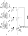
- FIG. 4A shows a schematic diagram of an exemplary design of an omni-band LNA 440 with a shared source degeneration inductor.
- Omni-band LNA 440 may be used for any one of LNAs 340 in FIG. 3 .
- omni-band LNA 440 includes three amplifier circuits 450a, 450b and 450c for three band groups of low-band, mid-band and high-band, respectively.
- each amplifier circuit 450 includes a gain transistor 454 coupled to a cascode transistor 456 and also to a multi-tap source degeneration inductor 452.
- a gain transistor 454a has its gate receiving an input RF signal (RFin) and its source coupled to one end of multi-tap inductor 452.
- Multi-tap inductor 452 has four taps A, B, C and D, with taps A and D corresponding to the two ends of inductor 452.
- Inductor 452 has tap A coupled to the source of gain transistor 454a and tap D coupled to circuit ground.
- a cascode transistor 456a has its source coupled to the drain of gain transistor 454a, its gate receiving a first enable control signal (Venb1) for low-band, and its drain coupled to an output of amplifier circuit 450a.
- Amplifier circuit 450b for mid-band includes a gain transistor 454b and a cascode transistor 456b, which are coupled in similar manner as gain transistor 454a and cascode transistor 456a in amplifier circuit 450a for low-band.
- Amplifier circuit 450c for high-band includes a gain transistor 454c and a cascode transistor 456c, which are also coupled in similar manner as gain transistor 454a and cascode transistor 456a in amplifier circuit 450a for low-band.
- the source of gain transistor 454b for mid-band is coupled to tap B of multi-tap inductor 452, and the source of gain transistor 454c for high-band is coupled to tap C of multi-tap inductor 452.
- Gain transistors 454a to 454c and cascode transistors 456a to 456c may be implemented with NMOS transistors, as shown in FIG. 4A , or with transistors of other types.
- Inductor 452 serves as source degeneration inductors for all three gain transistors 454a, 454b and 454c, which observe progressively smaller source inductances due to their connection at different taps of inductor 452.
- gain transistor 454c for high-band is coupled to tap C, which is closest to circuit ground, and hence observes the smallest source degeneration inductance.
- Gain transistor 454b for mid-band is coupled to higher tap B and hence observes a larger source degeneration inductance.
- Gain transistor 454a for low-band is coupled to the top end of inductor 452 at tap A and hence observes the largest source degeneration inductance.
- a variable capacitor 458 may be present across the gate and source of gain transistor 454a.
- Capacitor 458 may include parasitic capacitance of gain transistors 454a, 454b and 454c.
- Capacitor 458 may also include a bank of switchable capacitors, which may be coupled between the gate and source of gain transistor 454a and may be used to fine-tune the input impedance of omni-band LNA 440.
- Each switchable capacitor may be implemented with a capacitor coupled in series with a switch. The capacitors in the bank may be selected to obtain good input matching for omni-band LNA 440.
- Amplifier circuits 450a, 450b and 450c are coupled to three load circuits 470a, 470b and 470c, respectively.
- each load circuit 470 includes a transformer 472 comprising a primary coil 474 and a secondary coil 476.
- a coil may also be referred to as an inductor coil, a winding, a conductor, etc.
- a transformer 472a includes (i) a primary coil 474a coupled between the output of amplifier circuit 450a and a power supply (VDD) and (ii) a secondary coil 476a providing a first differential amplified RF signal (RFamp1) to a downconverter for low-band (not shown in FIG. 4A ).
- Load circuit 470b for mid-band includes a transformer 472b having (i) a primary coil 474b coupled between the output of amplifier circuit 450b and the VDD supply and (ii) a secondary coil 476b providing a second differential amplified RF signal (RFamp2) to a downconverter for mid-band (not shown in FIG. 4A ).
- Load circuit 470c for high-band includes a transformer 472c having (i) a primary coil 474c coupled between the output of amplifier circuit 450c and the VDD supply and (ii) a secondary coil 476c providing a third differential amplified RF signal (RFamp3) to a downconverter for high-band (not shown in FIG. 4A ).
- Transformers 472a, 472b and 472c are coupled to the drains of cascode transistors 456a, 456b and 456c, respectively.
- Transformers 472a, 472b and 472c may be designed to provide good performance for low-band, mid-band, and high-band, respectively.
- each load circuit 470 may be coupled to a separate downconverter.
- multiple load circuits 470 may be coupled to a shared downconverter via switches. The switches may be controlled to pass an amplified RF signal from one load circuit to the shared downconverter at any given moment.
- each downconverter may include two mixers to perform quadrature downconversion of an amplified RF signal from RF to either baseband or an intermediate frequency (IF).
- Load circuits 470 may also be implemented in other manners.
- a load circuit may include an inductor and possibly a capacitor coupled between the output of an amplifier circuit and the VDD supply.
- a load circuit may include a P-channel metal oxide semiconductor (PMOS) transistor having its source coupled to the VDD supply and its drain coupled to the drain of a cascode transistor 456. The PMOS transistor may provide an active load for cascode transistor 456.
- PMOS P-channel metal oxide semiconductor
- Amplifier circuits 450a, 450b and 450c may be implemented in various manners.
- gain transistors 454a, 454b and 454c may have similar transistor sizes, and cascode transistors 456a, 456b and 456c may also have similar transistor sizes.
- gain transistors 454a, 454b and 454c may have different transistor sizes and/or cascode transistors 456a, 456b and 456c may have different transistor sizes.
- gain transistors 454a, 454b and 454c may have similar bias currents, which may be selected to provide good performance for all three band groups.
- gain transistors 454a, 454b and 454c may have different bias currents. The bias current for each gain transistor 454 may be selected to provide good performance for the associated band group.
- the gain transistors 454a, 454b and 454c have different transistor sizes, or different bias currents, or both.
- FIG. 4A shows omni-band LNA 440 including three amplifier circuits 450a, 450b and 450c for three band groups.
- An omni-band LNA may include fewer or more than three amplifier circuits 450 for fewer or more band groups.
- Omni-band LNA 440 receives an input RF signal, which is applied to all three amplifier circuits 450a, 450b and 450c.
- the input RF signal may include one or more transmissions in one or more bands in a band group of interest, i.e., a selected band group.
- the amplifier circuit 450 for the selected band group may be enabled to amplify the input RF signal and provide an output RF signal for the selected band group.
- Load circuit 470 for the selected band group may receive the output RF signal from the enabled amplifier circuit 450 and provide an amplified RF signal for the selected band group.
- the remaining amplifier circuits 450 for other band groups may be disabled.
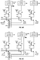
- FIG. 4B shows operation of omni-band LNA 440 when low-band is selected.
- amplifier circuit 450a is enabled to generate a first output RF signal (RFout1) for low-band by providing an appropriate bias voltage on the Venb1 signal at the gate of cascode transistor 456a.
- Load circuit 470a receives the RFout1 signal and provides the RFamp1 signal for low-band to a downconverter.
- Gain transistor 454a observes a large source degeneration inductance via the entire inductor 452.
- Amplifier circuits 450b and 450c are disabled by providing low voltages on the Venb2 and Venb3 signals at the gates of cascode transistors 456b and 456c, respectively.
- FIG. 4C shows operation of omni-band LNA 440 when mid-band is selected.
- amplifier circuit 450b is enabled to generate a second output RF signal (RFout2) for mid-band by providing an appropriate bias voltage on the Venb2 signal at the gate of cascode transistor 456b.
- Load circuit 470b receives the RFout2 signal and provides the RFamp2 signal for mid-band to a downconverter.
- Gain transistor 454b observes a medium source degeneration inductance via a portion of inductor 452 from tap B to circuit ground.
- Amplifier circuits 450a and 450c are disabled by providing low voltages on the Venb1 and Venb3 signals at the gates of cascode transistors 456a and 456c, respectively.
- FIG. 4D shows operation of omni-band LNA 440 when high-band is selected.
- amplifier circuit 450c is enabled to generate a third output RF signal (RFout3) for high-band by providing an appropriate bias voltage on the Venb3 signal at the gate of cascode transistor 456c.
- Load circuit 470c receives the RFout3 signal and provides the RFamp3 signal for high-band to a downconverter.
- Gain transistor 454c observes a small source degeneration inductance via a portion of inductor 452 from tap C to circuit ground.
- Amplifier circuits 450a and 450b are disabled by providing low voltages on the Venb1 and Venb2 signals at the gates of cascode transistors 456a and 456b, respectively.
- a gain transistor in an amplifier circuit may operate in (i) a saturation region when the amplifier circuit is enabled or (ii) a linear region when the amplifier circuit is disabled. Operating the gain transistor in the linear region when the amplifier circuit is disabled may reduce changes in the input impedance of omni-band LNA 440 regardless of which amplifier circuit or band group is selected.
- the input impedance of omni-band LNA 440 may be maintained within tolerable limits regardless of which amplifier circuit is selected and even with the change in the input impedance of the gain transistor. Maintaining the input impedance of omni-band LNA 440 within tolerable limits may improve power and/or impedance matching for all band groups.
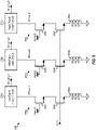
- FIG. 5 shows a schematic diagram of an exemplary design of an omni-band LNA 540 with separate source degeneration inductors.
- Omni-band LNA 540 may also be used for any one of LNAs 340 in FIG. 3 .
- omni-band LNA 540 includes three amplifier circuits 550a, 550b and 550c for low-band, mid-band, and high-band, respectively.
- Each amplifier circuit 550 includes a gain transistor 554 coupled to a cascode transistor 556 and also to a source degeneration inductor 552.
- a gain transistor 554a has its gate receiving an input RF signal and its source coupled to one end of an inductor 552a.
- a cascode transistor 556a has its source coupled to the drain of gain transistor 554a, its gate receiving a first enable control signal (Venb1) for low-band, and its drain coupled to an output of amplifier circuit 550a.
- Amplifier circuit 550b for mid-band includes a gain transistor 554b, a cascode transistor 556b, and an inductor 552b, which are coupled in similar manner as gain transistor 554a, cascode transistor 556a, and inductor 552a in amplifier circuit 550a for low-band.
- Amplifier circuit 550c for high-band includes a gain transistor 554c, a cascode transistor 556c, and an inductor 552c, which are coupled in similar manner as gain transistor 554a, cascode transistor 556a, and inductor 552a in amplifier circuit 550a for low-band.
- Inductors 552a, 552b and 552c may be designed to provide good performance for low-band, mid-band, and high-band, respectively.
- cascode transistors 556a, 556b, and 556c are coupled to load circuits 570a, 570b and 570c, respectively, which may comprise transformers (e.g., as shown in FIG. 4A ) and/or other circuits.
- Load circuits 570a, 570b and 570c may be designed to provide good performance for low-band, mid-band, and high-band, respectively.
- FIG. 6 shows a schematic diagram of an exemplary design of an omni-band LNA 640 without a source degeneration inductor.
- Omni-band LNA 640 may also be used for any one of LNAs 340 in FIG. 3 .
- omni-band LNA 640 includes a common gain transistor 654 and three cascode transistors 656a, 656b, and 656c for low-band, mid-band, and high-band, respectively.
- Gain transistor 654 has its gate receiving an input RF signal (RFin) and its source coupled to circuit ground.
- Cascode transistor 656a has its source coupled to the drain of gain transistor 654, its gate receiving a first enable control signal (Venb1) for low-band, and its drain coupled to a load circuit 670a for low-band.
- Cascode transistor 656b has its source coupled to the drain of gain transistor 654, its gate receiving a second enable control signal (Venb2) for mid-band, and its drain coupled to a load circuit 670b for mid-band.
- Cascode transistor 656c has its source coupled to the drain of gain transistor 654, its gate receiving a third enable control signal (Venb3) for high-band, and its drain coupled to a load circuit 670c for high-band.
- Load circuits 670a, 670b and 670c may comprise transformers (e.g., as shown in FIG. 4A ) and/or other circuits. Load circuits 670a, 670b and 670c may be designed to provide good performance for low-band, mid-band, and high-band, respectively.
- FIG. 7 shows a schematic diagram of an exemplary design of an omni-band LNA 442 with a shared source degeneration inductor and feedback.
- Omni-band LNA 442 may also be used for any one of LNAs 340 in FIG. 3 .
- omni-band LNA 442 includes three amplifier circuits 450a, 450b and 450c for low-band, mid-band, and high-band, respectively, as described above for FIG. 4A .
- Omni-band LNA 442 further includes a feedback circuit 460 coupled between the drains of cascode transistors 456a, 456b and 456c and the gates of gain transistors 454a, 454b and 454c, i.e., between the common input and the outputs of amplifier circuits 450a, 450b and 450c.
- feedback circuit 460 includes switches 462a, 462b, and 462c, a resistor 464, and a capacitor 466. Resistor 464 and capacitor 466 are coupled in series, with the bottom terminal of capacitor 466 being coupled to the gates of gain transistors 454a, 454b and 454c. Switches 462a, 462b, and 462c have one terminal coupled to resistor 464 and the other terminal coupled to the drains of cascode transistors 456a, 456b and 456c, respectively. Switches 462a, 462b, and 462c may each be closed to connect feedback circuit 460 to its associated cascode transistor 456 and may be opened to disconnect feedback circuit 460 from the associated cascode transistor 456. Feedback circuit 460 may also include one or more active circuits such as a transistor.
- feedback circuit 460 may be enabled and used for low-band to provide input power match. For mid-band and high-band, feedback circuit 460 may be disabled, and source degeneration inductor 452 is used for input power match. Feedback circuit 460 may also be used in other manners.
- Feedback circuit 460 may help with input matching for omni-band LNA 442.
- Feedback circuit 460 may also improve the linearity of amplifier circuits 450a, 450b and/or 450c.
- Each amplifier circuit 450 is linearized by (i) both source degeneration inductor 452 and feedback circuit 460 when associated switch 462 is closed or (ii) only source degeneration inductor 452 when associated switch 462 is opened.
- the improved linearity with feedback circuit 460 allows a smaller inductor 452 to be used to obtain the desired linearity.
- FIG. 8 shows a schematic diagram of an exemplary design of an omni-band LNA 840 with a tunable matching circuit 830.
- Omni-band LNA 840 may be implemented based on any of the omni-band LNA designs described above.
- Omni-band LNA 840 includes an input that receives an input RF signal (RFin) and K outputs that provide output RF signals (RFout1 to RFoutK) for K band groups, where K may be any integer value greater than one.
- Tunable matching circuit 830 is coupled to the input of omni-band LNA 840 and performs input matching for LNA 840.
- Matching circuit 830 receives a received RF signal (RFrx) and provides the input RF signal to omni-band LNA 840.
- RFrx received RF signal
- K load circuits 870a to 870k are coupled to the K outputs of omni-band LNA 840 and are designed for K band groups.
- Each load circuit 870 may comprise a transformer (e.g., as shown in FIG. 4A ) and/or other circuit components.
- Tunable matching circuit 830 may be implemented in various manners. Some exemplary designs of tunable matching circuit 830 are described below.
- FIG. 9A shows an exemplary design of a tunable matching circuit 830a based on an L topology.
- the L topology includes a series circuit component coupled to a shunt circuit component.
- a series circuit component is a circuit component connected between two nodes.
- a shunt circuit component is a circuit component connected between a node and circuit ground.
- a circuit component may be an inductor, a capacitor, a resistor, etc.
- Matching circuit 830a includes (i) a series inductor 912 coupled between the input and output of matching circuit 830a and (ii) a tunable shunt capacitor 914 coupled between the output of matching circuit 830a and circuit ground.
- FIG. 9B shows an exemplary design of a tunable matching circuit 830b based on the L topology.
- Matching circuit 830b includes (i) a tunable series capacitor 922 coupled between the input and output of matching circuit 830b and (ii) a shunt inductor 924 coupled between the output of matching circuit 830b and circuit ground.
- FIG. 9C shows an exemplary design of a tunable matching circuit 830c based on an R topology.
- the R topology includes a shunt circuit component coupled to a series circuit component.
- Matching circuit 830c includes (i) a tunable shunt capacitor 932 coupled between the input of matching circuit 830c and circuit ground and (ii) a series inductor 934 coupled between the input and output of matching circuit 830c.
- FIG. 9D shows an exemplary design of a tunable matching circuit 830d based on a Pi topology.
- the Pi topology includes a shunt circuit component coupled to a series circuit component, which is coupled to another shunt circuit component.
- Matching circuit 830d includes (i) a shunt capacitor 942 coupled between the input of matching circuit 830d and circuit ground, (ii) a series inductor 944 coupled between the input and output of matching circuit 830d, and (iii) a tunable shunt capacitor 946 coupled between the output of matching circuit 830d and circuit ground.
- FIG. 9E shows an exemplary design of a tunable matching circuit 830e with two R sections.
- Matching circuit 830e includes (i) a shunt inductor 952 coupled between the input of matching circuit 830e and the VDD supply, (ii) a series capacitor 954 coupled between the input of matching circuit 830e and node E, (iii) a tunable shunt capacitor 956 coupled between node E and circuit ground, and (iv) a series inductor 958 coupled between node E and the output of matching circuit 830e.
- FIG. 9F shows an exemplary design of a tunable matching circuit 830f based on the Pi topology.
- Matching circuit 830f includes (i) a shunt inductor 962 coupled between the input of matching circuit 830f and the VDD supply, (ii) a series capacitor 964 coupled between the input and output of matching circuit 830f, (iii) a tunable shunt capacitor 966 coupled between the output of matching circuit 830f and circuit ground, and (iv) a shunt inductor 968 coupled between the output of matching circuit 830f and circuit ground.
- a fixed matching circuit may also be implemented based on any of the exemplary designs shown in FIGS. 9A to 9F .
- each adjustable circuit component e.g., each adjustable capacitor
- a fixed circuit component e.g., a fixed capacitor
- Transformers for different band groups may be implemented in various manners.
- the primary and secondary coils of a transformer may be implemented with various patterns to obtain the desired inductance and coupling.
- the primary and secondary coils may also be fabricated on one or more conductive layers.
- FIG. 10 shows a top view of an exemplary design of three transformers for three band groups.
- the three transformers may be used for transformers 472a to 472c in FIG. 4A , load circuits 570a to 570c in FIG. 5 , load circuits 670a to 670c in FIG. 6 , or load circuits 870a to 870c in FIG. 8 .
- a transformer for low-band includes a primary coil 1074a formed in a spiral pattern on a first conductive layer.
- a transformer for mid-band includes a primary coil 1074b formed in a spiral pattern inside of primary coil 1074a on the first conductive layer.
- a transformer for high-band includes a primary coil 1074c formed in a spiral pattern inside of primary coil 1074b on the first conductive layer.
- a ground guard ring 1080 is located between primary coils 1074a and 1074b and provides isolation between these two primary coils.
- a ground guard ring 1082 is located between primary coils 1074b and 1074c and provides isolation between these primary coils.
- secondary coils for the three transformers may be arranged in a spiral pattern on a second conductive layer.
- the secondary coil for each transformer 1072 may be formed directly underneath the primary coil for that transformer.
- FIG. 10 shows an exemplary design in which three primary coils 1074a, 1074b and 1074c for three transformers for three band groups are formed inside of one another, which may save space.
- the primary and secondary coils of the transformers for different band groups may be implemented with any layout, any pattern, and any number of turns.
- the number of turns, the diameter of the turns, the width and height of each coil, the spacing between the primary and secondary coils for each transformer, and/or other attributes of the two coils may be selected to obtain the desired inductance and quality factor (Q) for each coil and the desired coupling coefficient between the coils.
- the coupling coefficient may be varied by controlling the placement of the coils and/or the distance between the coils.
- the stacked topology in FIG. 10 may allow the transformers to be fabricated in a smaller area and may also result in better matching between the two ends of the secondary coil for a differential design.
- Transformers may also be implemented with a side-by-side topology or other topologies. In general, different topologies, layout patterns, and fabrication techniques may provide different advantages for a transformer.
- the omni-band amplifiers may provide various advantages.
- First, an omni-band amplifier can support a wide frequency range covering multiple band groups, which may be highly desirable for new wireless devices that are required to support many bands in different band groups.
- Second, an omni-band amplifier may have good performance for all supported band groups, e.g., via use of a transformer and source degeneration for each band group.
- Third, an omni-band amplifier may reduce the number of input/output (I/O) pins on an IC chip since a single I/O pin can provide an input RF signal to support multiple band groups.
- Fourth, an omni-band amplifier may provide more flexibility since each I/O pin can be configured to support any band group.
- an IC may include 20 omni-band LNAs and may be configured to support (i) 20 low-band receivers, or (ii) 10 low-band receivers, 5 mid-band receivers, and 5 high-band receivers, or (iii) 10 mid-band receivers and 10 high-band receivers, or (iv) some other combination of receivers.
- the omni-band amplifiers may have other advantages.
- an apparatus e.g., a wireless device, an IC, a circuit module, etc.
- the at least one gain transistor receives an input RF signal and may have the input(s) coupled together.
- the plurality of cascode transistors e.g., cascode transistors 456) is coupled to the at least one gain transistor and provides an output RF signal for one of the plurality of band groups.
- the plurality of band groups may include low-band, mid-band, and/or high-band. Each band group may cover a plurality of bands.
- the at least one gain transistor may comprise a plurality of gain transistors (e.g., gain transistors 454) for the plurality of band groups.
- One of the plurality of gain transistors and one of the plurality of cascode transistors may be enabled to amplify the input RF signal and provide the output RF signal for the selected band group.
- the plurality of gain transistors may have different transistor sizes and/or different bias currents.
- the apparatus further comprises an inductor (e.g., inductor 452 in FIG. 4A ) having a plurality of taps coupled to the plurality of gain transistors and circuit ground.
- the apparatus may further comprise a plurality of inductors (e.g., inductors 552 in FIG. 5 ) coupled between the plurality of gain transistors and circuit ground.
- the at least one gain transistor may comprise a single gain transistor (e.g., gain transistor 654) coupled to the plurality of cascode transistors.
- This gain transistor may have its source coupled directly to circuit ground (e.g., as shown in FIG. 6 ) or to a source degeneration inductor.
- the apparatus may include a feedback circuit (e.g., feedback circuit 460 in FIG. 7 ) coupled between at least one of the plurality of cascode transistors and the at least one gain transistor.
- the feedback circuit may comprise a resistor, or a capacitor, or a transistor, or some other circuit component, or a combination thereof.
- the feedback circuit may be closed around a selected amplifier circuit, e.g., between a cascode transistor and a gain transistor for the selected amplifier circuit.
- the apparatus may further comprise a tunable matching circuit (e.g., tunable matching circuit 830 in FIG. 8 ) coupled to the at least one gain transistor.
- the tunable matching circuit may receive a received RF signal and provide the input RF signal.
- the tunable matching circuit may comprise at least one adjustable circuit component (e.g., an adjustable capacitor).
- the apparatus may further comprise a plurality of transformers (e.g., transformers 472 in FIG. 4A ) coupled to the plurality of cascode transistors.
- a plurality of transformers e.g., transformers 472 in FIG. 4A
- Each of the plurality of transformers may be used for one of the plurality of band groups.
- the at least one gain transistor may comprise a first gain transistor for a first band group and a second gain transistor for a second band group.
- the plurality of cascode transistors may comprise a first cascode transistor for the first band group and a second cascode transistor for the second band group.
- the first gain transistor may be coupled to the first cascode transistor.
- the second gain transistor may be coupled to the second cascode transistor.
- An inductor is coupled between the first gain transistor and circuit ground and comprises a tap coupled to the second gain transistor.
- a first transformer for the first band group may be coupled to the first cascode transistor.
- a second transformer for the second band group may be coupled to the second cascode transistor.
- the first transformer may comprise a first primary coil formed on a conductive layer.
- the second transformer may comprise a second primary coil formed within the first primary coil on the conductive layer (e.g., as shown in FIG. 10 ).
- the at least one gain transistor may further comprise a third gain transistor for a third band group.
- the plurality of cascode transistors may further comprise a third cascode transistor for the third band group.
- the third gain transistor may be coupled to the third cascode transistor.
- a third transformer for the third band group may be coupled to the third cascode transistor.
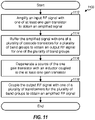
- FIG. 11 shows an exemplary design of a process 1100 for performing signal amplification.
- An input RF signal is amplified with one of at least one gain transistor to obtain an amplified signal (block 1112).
- the amplified signal is buffered with one of a plurality of cascode transistors for a plurality of band groups to obtain an output RF signal for one of the plurality of band groups (block 1114).
- the source of the one gain transistor may be degenerated with an inductor coupled to the at least one gain transistor (block 1116).
- the output RF signal may be coupled with one of a plurality of transformers for the plurality of band groups to obtain an amplified RF signal (block 1118).
- the omni-band amplifiers described herein may be implemented on an IC, an analog IC, an RFIC, a mixed-signal IC, an ASIC, a printed circuit board (PCB), an electronic device, etc.
- the omni-band amplifiers may also be fabricated with various IC process technologies such as complementary metal oxide semiconductor (CMOS), N-channel MOS (NMOS), P-channel MOS (PMOS), bipolar junction transistor (BJT), bipolar-CMOS (BiCMOS), silicon germanium (SiGe), gallium arsenide (GaAs), heterojunction bipolar transistors (HBTs), high electron mobility transistors (HEMTs), silicon-on-insulator (SOI), etc.
- CMOS complementary metal oxide semiconductor
- NMOS N-channel MOS
- PMOS P-channel MOS
- BJT bipolar junction transistor
- BiCMOS bipolar-CMOS
- SiGe silicon germanium
- GaAs gallium arsenide
- HBTs heterojunction bi
- An apparatus implementing an omni-band amplifier described herein may be a stand-alone device or may be part of a larger device.
- a device may be (i) a stand-alone IC, (ii) a set of one or more ICs that may include memory ICs for storing data and/or instructions, (iii) an RFIC such as an RF receiver (RFR) or an RF transmitter/receiver (RTR), (iv) an ASIC such as a mobile station modem (MSM), (v) a module that may be embedded within other devices, (vi) a receiver, cellular phone, wireless device, handset, or mobile unit, (vii) etc.
- RFR RF receiver
- RTR RF transmitter/receiver
- MSM mobile station modem
- the functions described may be implemented in hardware, software, firmware, or any combination thereof. If implemented in software, the functions may be stored on or transmitted over as one or more instructions or code on a computer-readable medium.
- Computer-readable media includes both computer storage media and communication media including any medium that facilitates transfer of a computer program from one place to another.
- a storage media may be any available media that can be accessed by a computer.
- such computer-readable media can comprise RAM, ROM, EEPROM, CD-ROM or other optical disk storage, magnetic disk storage or other magnetic storage devices, or any other medium that can be used to carry or store desired program code in the form of instructions or data structures and that can be accessed by a computer.
- any connection is properly termed a computer-readable medium.
- the software is transmitted from a website, server, or other remote source using a coaxial cable, fiber optic cable, twisted pair, digital subscriber line (DSL), or wireless technologies such as infrared, radio, and microwave
- the coaxial cable, fiber optic cable, twisted pair, DSL, or wireless technologies such as infrared, radio, and microwave are included in the definition of medium.
- Disk and disc includes compact disc (CD), laser disc, optical disc, digital versatile disc (DVD), floppy disk and blu-ray disc where disks usually reproduce data magnetically, while discs reproduce data optically with lasers. Combinations of the above should also be included within the scope of computer-readable media.
Description
- The present disclosure relates generally to electronics, and more specifically to amplifiers.
- A wireless device (e.g., a cellular phone or a smartphone) in a wireless communication system may transmit and receive data for two-way communication. The wireless device may include a transmitter for data transmission and a receiver for data reception. For data transmission, the transmitter may modulate a radio frequency (RF) carrier signal with data to obtain a modulated RF signal, amplify the modulated RF signal to obtain an amplified RF signal having the proper output power level, and transmit the amplified RF signal via an antenna to a base station. For data reception, the receiver may obtain a received RF signal via the antenna and may amplify and process the received RF signal to recover data sent by the base station.
- A wireless device may support operation over a wide frequency range. The wireless device may include a number of amplifiers, with each amplifier being designed to operate over a portion of the wide frequency range supported by the wireless device. It is desirable to support operation over a wide frequency range with as few amplifiers as possible.
- Attention is drawn to a paper by ITO T ET AL, entitled "Characterization of On-Chip Multiport Inductors for Small-Area RF Circuits", IEEE TRANSACTIONS ON CIRCUITS AND SYSTEMS I: REGULAR PAPERS, IEEE, US, vol. 56, no. 8, doi:10.1109/TCSI.2008.2010096, ISSN 1549-8328, pages 1590 - 1597. This paper proposes a calculation method to derive self and mutual components of each segment in multiport inductors. In the proposed method, a set of S-parameters of the multiport inductor is mathematically decomposed into several matrices, which express self and mutual effects of each segment in the inductor. Due to this mathematics-based method, the multiport inductor can be characterized without numerical extractions. In this paper, a small-area distributed amplifier (DA) utilizing five-port inductors is also demonstrated as an application of the proposed analysis method. In the experimental results using a 0.18-mum CMOS process, the three-stage DA utilizing two five-port inductors to replace eight two-port inductors shows that the multiport inductor can successfully reduce layout area.
- Attention is further drawn to a paper by ZHANG F ET AL, entitled "An Agile, Ultra-Wideband Pulse Radio Transceiver With Discrete-Time Wideband-IF", IEEE JOURNAL OF SOLID-STATE CIRCUITS, IEEE SERVICE CENTER, PISCATAWAY, NJ, USA, vol. 44, no. 5, doi:10.1109/JSSC.2009.2020681, ISSN 0018-9200, pages 1336 - 1351. The paper describes a pulse-based CMOS ultra-wideband transmitter and receiver which have been realized using a standard digital 90 nm CMOS process. The transceiver uses digital templates stored in high-speed memories for pulse generation on the transmit side and for correlation on the receive side. This allows fast band switching for multi-band operation and interferer avoidance without the requirement for fast-settling phase-locked loops. The receiver contains a 3.1-9.5 GHz broadband front-end and discrete-time intermediate frequency correlators that achieve a pulse rate of 100 Mpulses/s and has a die area of 1 mm 2 while consuming 130 mA from a 1.2 V supply. The transmitter uses interleaved, intermediate frequency digital-to-analog converters followed by partial-order hold reconstruction filters that eliminate sampling images, and a quadrature RF up-converter.
- Attention is drawn to a further paper by ZHANG F ET AL, entitled "Low power programmable-gain CMOS distributed LNA for ultra-wideband applications", VLSI CIRCUITS, 2005. DIGEST OF TECHNICAL PAPERS. 2005 SYMPOSIUM ON, IEEE, PISCATAWAY, NJ, USA, doi:10.1109/VLSIC.2005.1469338, ISBN 978-4-900784-01-7, pages 78 - 81. In the paper a design methodology is presented for low power distributed amplifiers and is used for the design of a 9 mW LNA with programmable gain.
- Attention is further drawn to a paper by KWANG-JIN KOH ET AL, entitled "A merged structure of LNA & sub-harmonic mixer for multi-band DCR applications", 2003 IEEE MTT-S INTERNATIONAL MICROWAVE SYMPOSIUM DIGEST (IMS 2003). PHILADELPHIA, PA, JUNE 8 - 13, 2003; IEEE MTT-S INTERNATIONAL MICROWAVE SYMPOSIUM, doi:10.1109/MWSYM.2003.1210925, ISBN 978-0-7803-7695-3, pages 243 - 246. The paper describes a merged structure of variable gain LNA and sub-harmonic mixer is designed for multi-band direct conversion receiver (DCR) applications.
- Further attention is drawn to
JP 2001 267864 A - The present invention is set forth in the independent claims, respectively. Preferred embodiments of the invention are described in the dependent claims.
-
-
FIG. 1 shows a wireless device communicating with a wireless system. -
FIG. 2 shows three exemplary band groups. -
FIG. 3 shows a block diagram of the wireless device inFIG. 1 . -
FIGS. 4A to 4D show an omni-band low noise amplifier (LNA) with a shared source degeneration inductor. -
FIG. 5 shows an omni-band LNA with separate source degeneration inductors. -
FIG. 6 shows an omni-band LNA without a source degeneration inductor. -
FIG. 7 shows an omni-band LNA with a shared source degeneration inductor and feedback. -
FIG. 8 shows an omni-band LNA with a tunable matching circuit. -
FIGS. 9A to 6F shows six exemplary designs of a tunable matching circuit. -
FIG. 10 shows a top view of three transformers for three band groups. -
FIG. 11 shows a process for performing signal amplification. - The detailed description set forth below is intended as a description of exemplary designs of the present disclosure and is not intended to represent the only designs in which the present disclosure can be practiced. The term "exemplary" is used herein to mean "serving as an example, instance, or illustration." Any design described herein as "exemplary" is not necessarily to be construed as preferred or advantageous over other designs. The detailed description includes specific details for the purpose of providing a thorough understanding of the exemplary designs of the present disclosure. It will be apparent to those skilled in the art that the exemplary designs described herein may be practiced without these specific details. In some instances, well-known structures and devices are shown in block diagram form in order to avoid obscuring the novelty of the exemplary designs presented herein.
- Omni-band amplifiers supporting a wide frequency range covering multiple band groups are disclosed herein. The omni-band amplifiers may also be referred to as universal amplifiers, etc. The omni-band amplifiers may be used for various types of electronic devices such as wireless communication devices.
-
FIG. 1 shows awireless device 110 communicating with awireless communication system 120.Wireless system 120 may be a Long Term Evolution (LTE) system, a Code Division Multiple Access (CDMA) system, a Global System for Mobile Communications (GSM) system, a wireless local area network (WLAN) system, or some other wireless system. A CDMA system may implement Wideband CDMA (WCDMA), CDMA IX, Evolution-Data Optimized (EVDO), Time Division Synchronous CDMA (TD-SCDMA), or some other version of CDMA. For simplicity,FIG. 1 showswireless system 120 including twobase stations system controller 140. In general, a wireless system may include any number of base stations and any set of network entities. -
Wireless device 110 may also be referred to as a user equipment (UE), a mobile station, a terminal, an access terminal, a subscriber unit, a station, etc.Wireless device 110 may be a cellular phone, a smartphone, a tablet, a wireless modem, a personal digital assistant (PDA), a handheld device, a laptop computer, a smartbook, a netbook, a cordless phone, a wireless local loop (WLL) station, a Bluetooth device, etc.Wireless device 110 may communicate withwireless system 120.Wireless device 110 may also receive signals from broadcast stations (e.g., a broadcast station 134), signals from satellites (e.g., a satellite 150) in one or more global navigation satellite systems (GNSS), etc.Wireless device 110 may support one or more radio technologies for wireless communication such as LTE, WCDMA, CDMA IX, EVDO, TD-SCDMA, GSM, 802.11, etc. -
FIG. 2 shows three exemplary band groups that may be supported bywireless device 110.Wireless device 110 may be able to operate in low-band (LB) covering frequencies lower than 1000 megahertz (MHz), mid-band (MB) covering frequencies from 1000 MHz to 2300 MHz, and/or high-band (HB) covering frequencies higher than 2300 MHz. For example, low-band may cover 698 to 960 MHz, mid-band may cover 1475 to 2170 MHz, and high-band may cover 2300 to 2690 MHz and 3400 to 3800 MHz, as shown inFIG. 2 . Low-band, mid-band, and high-band refer to three groups of bands (or band groups), with each band group including a number of frequency bands (or simply, "bands"). Each band may cover up to 200 MHz. LTE Release 11 supports 35 bands, which are referred to as LTE/UMTS bands and are listed in 3GPP TS 36.101. - In general, any number of band groups may be defined. Each band group may cover any range of frequencies, which may or may not match any of the frequency ranges shown in
FIG. 2 . Each band group may also include any number of bands. -
FIG. 3 shows a block diagram of an exemplary design ofwireless device 110 inFIG. 1 . In this exemplary design,wireless device 110 includes atransceiver 320 coupled to aprimary antenna 310, atransceiver 322 coupled to asecondary antenna 312, and a data processor/controller 380.Transceiver 320 includes multiple (K) receivers 330pa to 330pk and multiple (K) transmitters 350pa to 350pk to support multiple frequency bands, multiple radio technologies, carrier aggregation, etc.Transceiver 322 includes L receivers 330sa to 330sl and L transmitters 350sa to 350sl to support multiple frequency bands, multiple radio technologies, carrier aggregation, receive diversity, multiple-input multiple-output (MIMO) transmission from multiple transmit antennas to multiple receive antennas, etc. - In the exemplary design shown in
FIG. 3 , each receiver 330 includes an LNA 340 and receive circuits 342. For data reception,antenna 310 receives signals from base stations and/or other transmitter stations and provides a received RF signal, which is routed through anantenna interface circuit 324 and presented as an input RF signal to a selected receiver.Antenna interface circuit 324 may include switches, duplexers, transmit filters, receive filters, matching circuits, etc. The description below assumes that receiver 330pa is the selected receiver. Within receiver 330pa, an LNA 340pa amplifies the input RF signal and provides an output RF signal. Receive circuits 342pa downconvert the output RF signal from RF to baseband, amplify and filter the downconverted signal, and provide an analog input signal todata processor 380. Receive circuits 342pa may include mixers, filters, amplifiers, matching circuits, an oscillator, a local oscillator (LO) generator, a phase locked loop (PLL), etc. Each remaining receiver 330 intransceivers - In the exemplary design shown in
FIG. 3 , each transmitter 350 includes transmit circuits 352 and a power amplifier (PA) 354. For data transmission,data processor 380 processes (e.g., encodes and modulates) data to be transmitted and provides an analog output signal to a selected transmitter. The description below assumes that transmitter 350pa is the selected transmitter. Within transmitter 350pa, transmit circuits 352pa amplify, filter, and upconvert the analog output signal from baseband to RF and provide a modulated RF signal. Transmit circuits 352pa may include amplifiers, filters, mixers, matching circuits, an oscillator, an LO generator, a PLL, etc. A PA 354pa receives and amplifies the modulated RF signal and provides a transmit RF signal having the proper output power level. The transmit RF signal is routed throughantenna interface circuit 324 and transmitted viaantenna 310. Each remaining transmitter 350 intransceivers -
FIG. 3 shows an exemplary design of receiver 330 and transmitter 350. A receiver and a transmitter may also include other circuits not shown inFIG. 3 , such as filters, matching circuits, etc. All or a portion oftransceivers transceivers - Data processor/
controller 380 may perform various functions forwireless device 110. For example,data processor 380 may perform processing for data being received via receivers 330 and data being transmitted via transmitters 350.Controller 380 may control the operation of the various circuits withintransceivers memory 382 may store program codes and data for data processor/controller 380. Data processor/controller 380 may be implemented on one or more application specific integrated circuits (ASICs) and/or other ICs. -
Wireless device 110 may support multiple band groups, multiple radio technologies, and/or multiple antennas.Wireless device 110 may include a number of LNAs to support reception via the multiple band groups, multiple radio technologies, and/or multiple antennas. - In an aspect of the present disclosure, omni-band LNAs may be used to support reception via multiple band groups. An omni-band LNA is an LNA that supports multiple band groups and has (i) a single input for all supported band groups and (ii) multiple outputs for the multiple band groups, e.g., one output for each band group. An omni-band LNA may receive an input RF signal at its input and provide an output RF signal at one of its multiple outputs. An omni-band LNA covers multiple band groups and is different from a multi-band LNA that covers multiple bands in the same band group.
- Omni-band LNAs may be implemented with various circuit designs. Some exemplary designs of omni-band LNAs are described below. Omni-band LNAs may also be implemented with transistors of various types. Some exemplary designs of omni-band LNAs implemented with N-channel metal oxide semiconductor (NMOS) transistors are described below.
-
FIG. 4A shows a schematic diagram of an exemplary design of an omni-band LNA 440 with a shared source degeneration inductor. Omni-band LNA 440 may be used for any one of LNAs 340 inFIG. 3 . In the exemplary design shown inFIG. 4A , omni-band LNA 440 includes threeamplifier circuits - In the exemplary design, according to the invention, shown in
FIG. 4A , each amplifier circuit 450 includes a gain transistor 454 coupled to a cascode transistor 456 and also to a multi-tapsource degeneration inductor 452. Withinamplifier circuit 450a for low-band, again transistor 454a has its gate receiving an input RF signal (RFin) and its source coupled to one end ofmulti-tap inductor 452.Multi-tap inductor 452 has four taps A, B, C and D, with taps A and D corresponding to the two ends ofinductor 452.Inductor 452 has tap A coupled to the source ofgain transistor 454a and tap D coupled to circuit ground. Acascode transistor 456a has its source coupled to the drain ofgain transistor 454a, its gate receiving a first enable control signal (Venb1) for low-band, and its drain coupled to an output ofamplifier circuit 450a. -
Amplifier circuit 450b for mid-band includes again transistor 454b and acascode transistor 456b, which are coupled in similar manner asgain transistor 454a andcascode transistor 456a inamplifier circuit 450a for low-band.Amplifier circuit 450c for high-band includes again transistor 454c and acascode transistor 456c, which are also coupled in similar manner asgain transistor 454a andcascode transistor 456a inamplifier circuit 450a for low-band. The source ofgain transistor 454b for mid-band is coupled to tap B ofmulti-tap inductor 452, and the source ofgain transistor 454c for high-band is coupled to tap C ofmulti-tap inductor 452.Gain transistors 454a to 454c andcascode transistors 456a to 456c may be implemented with NMOS transistors, as shown inFIG. 4A , or with transistors of other types. -
Inductor 452 serves as source degeneration inductors for all threegain transistors inductor 452. In particular,gain transistor 454c for high-band is coupled to tap C, which is closest to circuit ground, and hence observes the smallest source degeneration inductance.Gain transistor 454b for mid-band is coupled to higher tap B and hence observes a larger source degeneration inductance.Gain transistor 454a for low-band is coupled to the top end ofinductor 452 at tap A and hence observes the largest source degeneration inductance. - In the exemplary design, according to the invention, shown in
FIG. 4A , avariable capacitor 458 may be present across the gate and source ofgain transistor 454a.Capacitor 458 may include parasitic capacitance ofgain transistors Capacitor 458 may also include a bank of switchable capacitors, which may be coupled between the gate and source ofgain transistor 454a and may be used to fine-tune the input impedance of omni-band LNA 440. Each switchable capacitor may be implemented with a capacitor coupled in series with a switch. The capacitors in the bank may be selected to obtain good input matching for omni-band LNA 440. -
Amplifier circuits load circuits FIG. 4A , each load circuit 470 includes a transformer 472 comprising a primary coil 474 and a secondary coil 476. A coil may also be referred to as an inductor coil, a winding, a conductor, etc. Withinload circuit 470a for low-band, atransformer 472a includes (i) aprimary coil 474a coupled between the output ofamplifier circuit 450a and a power supply (VDD) and (ii) asecondary coil 476a providing a first differential amplified RF signal (RFamp1) to a downconverter for low-band (not shown inFIG. 4A ).Load circuit 470b for mid-band includes atransformer 472b having (i) aprimary coil 474b coupled between the output ofamplifier circuit 450b and the VDD supply and (ii) asecondary coil 476b providing a second differential amplified RF signal (RFamp2) to a downconverter for mid-band (not shown inFIG. 4A ).Load circuit 470c for high-band includes atransformer 472c having (i) aprimary coil 474c coupled between the output ofamplifier circuit 450c and the VDD supply and (ii) asecondary coil 476c providing a third differential amplified RF signal (RFamp3) to a downconverter for high-band (not shown inFIG. 4A ).Transformers cascode transistors Transformers - In one exemplary design, each load circuit 470 may be coupled to a separate downconverter. In another exemplary design, multiple load circuits 470 may be coupled to a shared downconverter via switches. The switches may be controlled to pass an amplified RF signal from one load circuit to the shared downconverter at any given moment. For both exemplary designs, each downconverter may include two mixers to perform quadrature downconversion of an amplified RF signal from RF to either baseband or an intermediate frequency (IF).
- Load circuits 470 may also be implemented in other manners. In another exemplary design, a load circuit may include an inductor and possibly a capacitor coupled between the output of an amplifier circuit and the VDD supply. In yet another exemplary design, a load circuit may include a P-channel metal oxide semiconductor (PMOS) transistor having its source coupled to the VDD supply and its drain coupled to the drain of a cascode transistor 456. The PMOS transistor may provide an active load for cascode transistor 456.
-
Amplifier circuits gain transistors cascode transistors gain transistors cascode transistors gain transistors gain transistors gain transistors -
FIG. 4A shows omni-band LNA 440 including threeamplifier circuits - Omni-
band LNA 440 receives an input RF signal, which is applied to all threeamplifier circuits -
FIG. 4B shows operation of omni-band LNA 440 when low-band is selected. In this case,amplifier circuit 450a is enabled to generate a first output RF signal (RFout1) for low-band by providing an appropriate bias voltage on the Venb1 signal at the gate ofcascode transistor 456a.Load circuit 470a receives the RFout1 signal and provides the RFamp1 signal for low-band to a downconverter.Gain transistor 454a observes a large source degeneration inductance via theentire inductor 452.Amplifier circuits cascode transistors -
FIG. 4C shows operation of omni-band LNA 440 when mid-band is selected. In this case,amplifier circuit 450b is enabled to generate a second output RF signal (RFout2) for mid-band by providing an appropriate bias voltage on the Venb2 signal at the gate ofcascode transistor 456b.Load circuit 470b receives the RFout2 signal and provides the RFamp2 signal for mid-band to a downconverter.Gain transistor 454b observes a medium source degeneration inductance via a portion ofinductor 452 from tap B to circuit ground.Amplifier circuits cascode transistors -
FIG. 4D shows operation of omni-band LNA 440 when high-band is selected. In this case,amplifier circuit 450c is enabled to generate a third output RF signal (RFout3) for high-band by providing an appropriate bias voltage on the Venb3 signal at the gate ofcascode transistor 456c.Load circuit 470c receives the RFout3 signal and provides the RFamp3 signal for high-band to a downconverter.Gain transistor 454c observes a small source degeneration inductance via a portion ofinductor 452 from tap C to circuit ground.Amplifier circuits cascode transistors - In an exemplary design, a gain transistor in an amplifier circuit may operate in (i) a saturation region when the amplifier circuit is enabled or (ii) a linear region when the amplifier circuit is disabled. Operating the gain transistor in the linear region when the amplifier circuit is disabled may reduce changes in the input impedance of omni-
band LNA 440 regardless of which amplifier circuit or band group is selected. The input capacitance (CIN) of a gain transistor may be expressed as:

- where W is the width and L is the length of the gain transistor, and
- Cox is a gate oxide capacitance of the gain transistor.
- As shown in equations (1) and (2), there may be a finite change in the input impedance of a gain transistor depending on whether an amplifier circuit is enabled or disabled. However, the input impedance of omni-
band LNA 440 may be maintained within tolerable limits regardless of which amplifier circuit is selected and even with the change in the input impedance of the gain transistor. Maintaining the input impedance of omni-band LNA 440 within tolerable limits may improve power and/or impedance matching for all band groups. -
FIG. 5 shows a schematic diagram of an exemplary design of an omni-band LNA 540 with separate source degeneration inductors. Omni-band LNA 540 may also be used for any one of LNAs 340 inFIG. 3 . In the exemplary design shown inFIG. 5 , omni-band LNA 540 includes threeamplifier circuits amplifier circuit 550a for low-band, again transistor 554a has its gate receiving an input RF signal and its source coupled to one end of aninductor 552a. The other end ofinductor 552a is coupled to circuit ground. Acascode transistor 556a has its source coupled to the drain ofgain transistor 554a, its gate receiving a first enable control signal (Venb1) for low-band, and its drain coupled to an output ofamplifier circuit 550a. -
Amplifier circuit 550b for mid-band includes again transistor 554b, acascode transistor 556b, and aninductor 552b, which are coupled in similar manner asgain transistor 554a,cascode transistor 556a, andinductor 552a inamplifier circuit 550a for low-band.Amplifier circuit 550c for high-band includes again transistor 554c, acascode transistor 556c, and aninductor 552c, which are coupled in similar manner asgain transistor 554a,cascode transistor 556a, andinductor 552a inamplifier circuit 550a for low-band.Inductors cascode transistors circuits FIG. 4A ) and/or other circuits.Load circuits -
FIG. 6 shows a schematic diagram of an exemplary design of an omni-band LNA 640 without a source degeneration inductor. Omni-band LNA 640 may also be used for any one of LNAs 340 inFIG. 3 . In the exemplary design shown inFIG. 6 , omni-band LNA 640 includes acommon gain transistor 654 and threecascode transistors Gain transistor 654 has its gate receiving an input RF signal (RFin) and its source coupled to circuit ground.Cascode transistor 656a has its source coupled to the drain ofgain transistor 654, its gate receiving a first enable control signal (Venb1) for low-band, and its drain coupled to aload circuit 670a for low-band.Cascode transistor 656b has its source coupled to the drain ofgain transistor 654, its gate receiving a second enable control signal (Venb2) for mid-band, and its drain coupled to aload circuit 670b for mid-band.Cascode transistor 656c has its source coupled to the drain ofgain transistor 654, its gate receiving a third enable control signal (Venb3) for high-band, and its drain coupled to aload circuit 670c for high-band.Load circuits FIG. 4A ) and/or other circuits.Load circuits -
FIG. 7 shows a schematic diagram of an exemplary design of an omni-band LNA 442 with a shared source degeneration inductor and feedback. Omni-band LNA 442 may also be used for any one of LNAs 340 inFIG. 3 . In the exemplary design shown inFIG. 7 , omni-band LNA 442 includes threeamplifier circuits FIG. 4A . Omni-band LNA 442 further includes afeedback circuit 460 coupled between the drains ofcascode transistors gain transistors amplifier circuits - In the exemplary design shown in
FIG. 7 ,feedback circuit 460 includesswitches resistor 464, and acapacitor 466.Resistor 464 andcapacitor 466 are coupled in series, with the bottom terminal ofcapacitor 466 being coupled to the gates ofgain transistors Switches resistor 464 and the other terminal coupled to the drains ofcascode transistors Switches feedback circuit 460 to its associated cascode transistor 456 and may be opened to disconnectfeedback circuit 460 from the associated cascode transistor 456.Feedback circuit 460 may also include one or more active circuits such as a transistor. - In an exemplary design,
feedback circuit 460 may be enabled and used for low-band to provide input power match. For mid-band and high-band,feedback circuit 460 may be disabled, andsource degeneration inductor 452 is used for input power match.Feedback circuit 460 may also be used in other manners. -
Feedback circuit 460 may help with input matching for omni-band LNA 442.Feedback circuit 460 may also improve the linearity ofamplifier circuits source degeneration inductor 452 andfeedback circuit 460 when associated switch 462 is closed or (ii) onlysource degeneration inductor 452 when associated switch 462 is opened. The improved linearity withfeedback circuit 460 allows asmaller inductor 452 to be used to obtain the desired linearity. -
FIG. 8 shows a schematic diagram of an exemplary design of an omni-band LNA 840 with atunable matching circuit 830. Omni-band LNA 840 may be implemented based on any of the omni-band LNA designs described above. Omni-band LNA 840 includes an input that receives an input RF signal (RFin) and K outputs that provide output RF signals (RFout1 to RFoutK) for K band groups, where K may be any integer value greater than one. Tunable matchingcircuit 830 is coupled to the input of omni-band LNA 840 and performs input matching forLNA 840.Matching circuit 830 receives a received RF signal (RFrx) and provides the input RF signal to omni-band LNA 840.K load circuits 870a to 870k are coupled to the K outputs of omni-band LNA 840 and are designed for K band groups. Each load circuit 870 may comprise a transformer (e.g., as shown inFIG. 4A ) and/or other circuit components. - Tunable matching
circuit 830 may be implemented in various manners. Some exemplary designs oftunable matching circuit 830 are described below. -
FIG. 9A shows an exemplary design of atunable matching circuit 830a based on an L topology. The L topology includes a series circuit component coupled to a shunt circuit component. A series circuit component is a circuit component connected between two nodes. A shunt circuit component is a circuit component connected between a node and circuit ground. A circuit component may be an inductor, a capacitor, a resistor, etc.Matching circuit 830a includes (i) aseries inductor 912 coupled between the input and output of matchingcircuit 830a and (ii) atunable shunt capacitor 914 coupled between the output of matchingcircuit 830a and circuit ground. -
FIG. 9B shows an exemplary design of atunable matching circuit 830b based on the L topology.Matching circuit 830b includes (i) atunable series capacitor 922 coupled between the input and output of matchingcircuit 830b and (ii) ashunt inductor 924 coupled between the output of matchingcircuit 830b and circuit ground. -
FIG. 9C shows an exemplary design of atunable matching circuit 830c based on an R topology. The R topology includes a shunt circuit component coupled to a series circuit component.Matching circuit 830c includes (i) atunable shunt capacitor 932 coupled between the input of matchingcircuit 830c and circuit ground and (ii) aseries inductor 934 coupled between the input and output of matchingcircuit 830c. -
FIG. 9D shows an exemplary design of atunable matching circuit 830d based on a Pi topology. The Pi topology includes a shunt circuit component coupled to a series circuit component, which is coupled to another shunt circuit component.Matching circuit 830d includes (i) ashunt capacitor 942 coupled between the input of matchingcircuit 830d and circuit ground, (ii) aseries inductor 944 coupled between the input and output of matchingcircuit 830d, and (iii) atunable shunt capacitor 946 coupled between the output of matchingcircuit 830d and circuit ground. -
FIG. 9E shows an exemplary design of atunable matching circuit 830e with two R sections.Matching circuit 830e includes (i) ashunt inductor 952 coupled between the input of matchingcircuit 830e and the VDD supply, (ii) aseries capacitor 954 coupled between the input of matchingcircuit 830e and node E, (iii) atunable shunt capacitor 956 coupled between node E and circuit ground, and (iv) aseries inductor 958 coupled between node E and the output of matchingcircuit 830e. -
FIG. 9F shows an exemplary design of atunable matching circuit 830f based on the Pi topology.Matching circuit 830f includes (i) ashunt inductor 962 coupled between the input of matchingcircuit 830f and the VDD supply, (ii) aseries capacitor 964 coupled between the input and output of matchingcircuit 830f, (iii) atunable shunt capacitor 966 coupled between the output of matchingcircuit 830f and circuit ground, and (iv) ashunt inductor 968 coupled between the output of matchingcircuit 830f and circuit ground. - A fixed matching circuit may also be implemented based on any of the exemplary designs shown in
FIGS. 9A to 9F . In this case, each adjustable circuit component (e.g., each adjustable capacitor) may be replaced with a fixed circuit component (e.g., a fixed capacitor). - Transformers for different band groups may be implemented in various manners. The primary and secondary coils of a transformer may be implemented with various patterns to obtain the desired inductance and coupling. The primary and secondary coils may also be fabricated on one or more conductive layers.
-
FIG. 10 shows a top view of an exemplary design of three transformers for three band groups. The three transformers may be used fortransformers 472a to 472c inFIG. 4A ,load circuits 570a to 570c inFIG. 5 ,load circuits 670a to 670c inFIG. 6 , orload circuits 870a to 870c inFIG. 8 . - In the exemplary design shown in
FIG. 10 , a transformer for low-band includes aprimary coil 1074a formed in a spiral pattern on a first conductive layer. A transformer for mid-band includes aprimary coil 1074b formed in a spiral pattern inside ofprimary coil 1074a on the first conductive layer. A transformer for high-band includes aprimary coil 1074c formed in a spiral pattern inside ofprimary coil 1074b on the first conductive layer. A ground guard ring 1080 is located betweenprimary coils ground guard ring 1082 is located betweenprimary coils - In an exemplary design, secondary coils for the three transformers may be arranged in a spiral pattern on a second conductive layer. The secondary coil for each transformer 1072 may be formed directly underneath the primary coil for that transformer.
-
FIG. 10 shows an exemplary design in which threeprimary coils - The stacked topology in
FIG. 10 may allow the transformers to be fabricated in a smaller area and may also result in better matching between the two ends of the secondary coil for a differential design. Transformers may also be implemented with a side-by-side topology or other topologies. In general, different topologies, layout patterns, and fabrication techniques may provide different advantages for a transformer. - The omni-band amplifiers (e.g., LNAs) described herein may provide various advantages. First, an omni-band amplifier can support a wide frequency range covering multiple band groups, which may be highly desirable for new wireless devices that are required to support many bands in different band groups. Second, an omni-band amplifier may have good performance for all supported band groups, e.g., via use of a transformer and source degeneration for each band group. Third, an omni-band amplifier may reduce the number of input/output (I/O) pins on an IC chip since a single I/O pin can provide an input RF signal to support multiple band groups. Fourth, an omni-band amplifier may provide more flexibility since each I/O pin can be configured to support any band group. For example, an IC may include 20 omni-band LNAs and may be configured to support (i) 20 low-band receivers, or (ii) 10 low-band receivers, 5 mid-band receivers, and 5 high-band receivers, or (iii) 10 mid-band receivers and 10 high-band receivers, or (iv) some other combination of receivers. The omni-band amplifiers may have other advantages.
- In an exemplary design, according to the invention, an apparatus (e.g., a wireless device, an IC, a circuit module, etc.) includes at least one gain transistor and a plurality of cascode transistors for a plurality of band groups. The at least one gain transistor (e.g., gain transistors 454 in
FIG. 4A ) receives an input RF signal and may have the input(s) coupled together. The plurality of cascode transistors (e.g., cascode transistors 456) is coupled to the at least one gain transistor and provides an output RF signal for one of the plurality of band groups. The plurality of band groups may include low-band, mid-band, and/or high-band. Each band group may cover a plurality of bands. - In an exemplary design, according to the invention, that is shown in
FIG. 4A , the at least one gain transistor may comprise a plurality of gain transistors (e.g., gain transistors 454) for the plurality of band groups. One of the plurality of gain transistors and one of the plurality of cascode transistors may be enabled to amplify the input RF signal and provide the output RF signal for the selected band group. In an exemplary design, the plurality of gain transistors may have different transistor sizes and/or different bias currents. In an exemplary design, the apparatus further comprises an inductor (e.g.,inductor 452 inFIG. 4A ) having a plurality of taps coupled to the plurality of gain transistors and circuit ground. In another exemplary design, the apparatus may further comprise a plurality of inductors (e.g., inductors 552 inFIG. 5 ) coupled between the plurality of gain transistors and circuit ground. - In another exemplary design that is shown in
FIG. 6 , the at least one gain transistor may comprise a single gain transistor (e.g., gain transistor 654) coupled to the plurality of cascode transistors. This gain transistor may have its source coupled directly to circuit ground (e.g., as shown inFIG. 6 ) or to a source degeneration inductor. - In an exemplary design, the apparatus may include a feedback circuit (e.g.,
feedback circuit 460 inFIG. 7 ) coupled between at least one of the plurality of cascode transistors and the at least one gain transistor. The feedback circuit may comprise a resistor, or a capacitor, or a transistor, or some other circuit component, or a combination thereof. The feedback circuit may be closed around a selected amplifier circuit, e.g., between a cascode transistor and a gain transistor for the selected amplifier circuit. - In an exemplary design, the apparatus may further comprise a tunable matching circuit (e.g.,
tunable matching circuit 830 inFIG. 8 ) coupled to the at least one gain transistor. The tunable matching circuit may receive a received RF signal and provide the input RF signal. The tunable matching circuit may comprise at least one adjustable circuit component (e.g., an adjustable capacitor). - In an exemplary design, the apparatus may further comprise a plurality of transformers (e.g., transformers 472 in
FIG. 4A ) coupled to the plurality of cascode transistors. Each of the plurality of transformers may be used for one of the plurality of band groups. - In an exemplary design, the at least one gain transistor may comprise a first gain transistor for a first band group and a second gain transistor for a second band group. The plurality of cascode transistors may comprise a first cascode transistor for the first band group and a second cascode transistor for the second band group. The first gain transistor may be coupled to the first cascode transistor. The second gain transistor may be coupled to the second cascode transistor. An inductor is coupled between the first gain transistor and circuit ground and comprises a tap coupled to the second gain transistor. A first transformer for the first band group may be coupled to the first cascode transistor. A second transformer for the second band group may be coupled to the second cascode transistor. The first transformer may comprise a first primary coil formed on a conductive layer. The second transformer may comprise a second primary coil formed within the first primary coil on the conductive layer (e.g., as shown in
FIG. 10 ). - In an exemplary design, the at least one gain transistor may further comprise a third gain transistor for a third band group. The plurality of cascode transistors may further comprise a third cascode transistor for the third band group. The third gain transistor may be coupled to the third cascode transistor. A third transformer for the third band group may be coupled to the third cascode transistor.
-
FIG. 11 shows an exemplary design of aprocess 1100 for performing signal amplification. An input RF signal is amplified with one of at least one gain transistor to obtain an amplified signal (block 1112). The amplified signal is buffered with one of a plurality of cascode transistors for a plurality of band groups to obtain an output RF signal for one of the plurality of band groups (block 1114). The source of the one gain transistor may be degenerated with an inductor coupled to the at least one gain transistor (block 1116). The output RF signal may be coupled with one of a plurality of transformers for the plurality of band groups to obtain an amplified RF signal (block 1118). - The omni-band amplifiers described herein may be implemented on an IC, an analog IC, an RFIC, a mixed-signal IC, an ASIC, a printed circuit board (PCB), an electronic device, etc. The omni-band amplifiers may also be fabricated with various IC process technologies such as complementary metal oxide semiconductor (CMOS), N-channel MOS (NMOS), P-channel MOS (PMOS), bipolar junction transistor (BJT), bipolar-CMOS (BiCMOS), silicon germanium (SiGe), gallium arsenide (GaAs), heterojunction bipolar transistors (HBTs), high electron mobility transistors (HEMTs), silicon-on-insulator (SOI), etc.
- An apparatus implementing an omni-band amplifier described herein may be a stand-alone device or may be part of a larger device. A device may be (i) a stand-alone IC, (ii) a set of one or more ICs that may include memory ICs for storing data and/or instructions, (iii) an RFIC such as an RF receiver (RFR) or an RF transmitter/receiver (RTR), (iv) an ASIC such as a mobile station modem (MSM), (v) a module that may be embedded within other devices, (vi) a receiver, cellular phone, wireless device, handset, or mobile unit, (vii) etc.
- In one or more exemplary designs, the functions described may be implemented in hardware, software, firmware, or any combination thereof. If implemented in software, the functions may be stored on or transmitted over as one or more instructions or code on a computer-readable medium. Computer-readable media includes both computer storage media and communication media including any medium that facilitates transfer of a computer program from one place to another. A storage media may be any available media that can be accessed by a computer. By way of example, and not limitation, such computer-readable media can comprise RAM, ROM, EEPROM, CD-ROM or other optical disk storage, magnetic disk storage or other magnetic storage devices, or any other medium that can be used to carry or store desired program code in the form of instructions or data structures and that can be accessed by a computer. Also, any connection is properly termed a computer-readable medium. For example, if the software is transmitted from a website, server, or other remote source using a coaxial cable, fiber optic cable, twisted pair, digital subscriber line (DSL), or wireless technologies such as infrared, radio, and microwave, then the coaxial cable, fiber optic cable, twisted pair, DSL, or wireless technologies such as infrared, radio, and microwave are included in the definition of medium. Disk and disc, as used herein, includes compact disc (CD), laser disc, optical disc, digital versatile disc (DVD), floppy disk and blu-ray disc where disks usually reproduce data magnetically, while discs reproduce data optically with lasers. Combinations of the above should also be included within the scope of computer-readable media.
- The previous description of the disclosure is provided to enable any person skilled in the art to make or use the disclosure. Various modifications to the disclosure will be readily apparent to those skilled in the art, and the generic principles defined herein may be applied to other variations without departing from the scope of the claims. Thus, the disclosure is not intended to be limited to the examples and designs described herein but is to be accorded the widest scope consistent with the principles and novel features disclosed herein.
Claims (11)
- An apparatus comprising:at least one gain transistor (454a, 454b, 454c) configured to receive an input radio frequency, RF, signal; anda plurality of cascode transistors (456a, 456b, 456c) for a plurality of band groups coupled to the at least one gain transistor (454a, 454b, 454c) and configured to provide an output RF signal for one of the plurality of band groups;the at least one gain transistor (454a, 454b, 454c) comprising a plurality of gain transistors for the plurality of band groups;the plurality of gain transistors (454a, 454b, 454c) having different transistor sizes, or different bias currents, or both;the at least one gain transistor (454a, 454b) comprising a first gain transistor (454a) for a first band group and a second gain transistor (454b) for a second band group, andthe plurality of cascode transistors (456a, 456b) comprising a first cascode transistor (456a) for the first band group and a second cascode transistor (456b) for the second band group; andcharacterized in further comprising:
an inductor (452) coupled between a source of the first gain transistor (454a) and circuit ground and comprising a tap coupled to the second gain transistor (454b). - The apparatus of claim 1, further comprising:
a feedback circuit coupled between at least one of the plurality of cascode transistors (456a, 456b, 456c) and the at least one gain transistor (454a, 454b, 454c). - The apparatus of claim 1, further comprising:
a tunable matching circuit coupled to the at least one gain transistor (454a, 454b, 454c) and configured to receive a received RF signal and provide the input RF signal. - The apparatus of claim 1, further comprising:
a plurality of transformers (470a, 470b, 470c) coupled to the plurality of cascode transistors (456a, 456b, 456c), each of the plurality of transformers being used for one of the plurality of band groups. - The apparatus of claim 1, further comprising:a first transformer (470a) for the first band group coupled to the first cascode transistor (456a), anda second transformer (470b) for the second band group coupled to the second cascode transistor (456b).
- The apparatus of claim 5, the first transformer comprising a first primary coil formed on a conductive layer, and the second transformer comprising a second primary coil formed within the first primary coil on the conductive layer.
- The apparatus of claim 1, the at least one gain transistor further comprising a third gain transistor (456c) for a third band group, and the plurality of cascode transistors further comprising a third cascode transistor (456c) for the third band group.
- The apparatus of claim 1, the plurality of band groups including at least one of low-band, mid-band, and high-band.
- A method comprising:amplifying (1112) an input radio frequency, RF, signal with one of at least one gain transistor (454a, 454b, 454c) to obtain an amplified signal; andbuffering (1114) the amplified signal with one of a plurality of cascode transistors (456a, 456b, 456c) for a plurality of band groups to obtain an output RF signal for one of the plurality of band groups; and whereinthe at least one gain transistor (454a, 454b, 454c) comprising a plurality of gain transistors for the plurality of band groups; andthe plurality of gain transistors (454a, 454b, 454c) having different transistor sizes, or different bias currents, or both.the at least one gain transistor (454a, 454b) comprising a first gain transistor (454a) for a first band group and a second gain transistor (454b) for a second band group, and wherein an inductor (452) is coupled between a source of the first gain transistor (454a) and circuit ground and comprising a tap coupled to the second gain transistor (454b); andthe plurality of cascode transistors (456a, 456b) comprising a first cascode transistor (456a) for the first band group and a second cascode transistor (456b) for the second band group.
- The method of claim 9, further comprising:
degenerating (1116) a source of the one gain transistor (454a, 454b, 454c) with the inductor coupled to the at least one gain transistor. - The method of claim 9, further comprising:
coupling (1118) the output RF signal with one of a plurality of transformers for the plurality of band groups to obtain an amplified RF signal.
Priority Applications (1)
| Application Number | Priority Date | Filing Date | Title |
|---|---|---|---|
| EP22205538.6A EP4164123A3 (en) | 2012-11-14 | 2013-11-12 | Omni-band amplifiers |
Applications Claiming Priority (2)
| Application Number | Priority Date | Filing Date | Title |
|---|---|---|---|
| US13/677,017 US9603187B2 (en) | 2012-11-14 | 2012-11-14 | Omni-band amplifiers |
| PCT/US2013/069752 WO2014078333A2 (en) | 2012-11-14 | 2013-11-12 | Omni-band amplifiers |
Related Child Applications (2)
| Application Number | Title | Priority Date | Filing Date |
|---|---|---|---|
| EP22205538.6A Division EP4164123A3 (en) | 2012-11-14 | 2013-11-12 | Omni-band amplifiers |
| EP22205538.6A Division-Into EP4164123A3 (en) | 2012-11-14 | 2013-11-12 | Omni-band amplifiers |
Publications (2)
| Publication Number | Publication Date |
|---|---|
| EP2920879A2 EP2920879A2 (en) | 2015-09-23 |
| EP2920879B1 true EP2920879B1 (en) | 2022-12-21 |
Family
ID=49725347
Family Applications (2)
| Application Number | Title | Priority Date | Filing Date |
|---|---|---|---|
| EP22205538.6A Pending EP4164123A3 (en) | 2012-11-14 | 2013-11-12 | Omni-band amplifiers |
| EP13802154.8A Active EP2920879B1 (en) | 2012-11-14 | 2013-11-12 | Omni-band amplifiers |
Family Applications Before (1)
| Application Number | Title | Priority Date | Filing Date |
|---|---|---|---|
| EP22205538.6A Pending EP4164123A3 (en) | 2012-11-14 | 2013-11-12 | Omni-band amplifiers |
Country Status (6)
| Country | Link |
|---|---|
| US (1) | US9603187B2 (en) |
| EP (2) | EP4164123A3 (en) |
| JP (1) | JP2015534420A (en) |
| KR (1) | KR20150084908A (en) |
| CN (1) | CN104798299B (en) |
| WO (1) | WO2014078333A2 (en) |
Families Citing this family (24)
| Publication number | Priority date | Publication date | Assignee | Title |
|---|---|---|---|---|
| US9473336B2 (en) * | 2014-05-16 | 2016-10-18 | Qualcomm Incorporated | Radio frequency (RF) front end having multiple low noise amplifier modules |
| US9723560B2 (en) * | 2014-05-22 | 2017-08-01 | Qualcomm Incorporated | Multi-stage amplifier with RC network |
| US9479131B2 (en) | 2014-05-23 | 2016-10-25 | Qualcomm Incorporated | Carrier aggregation amplifier with dual gain control |
| US9300264B2 (en) | 2014-08-22 | 2016-03-29 | Mediatek Inc. | Receiver arrangement and method of performing operations of receiver |
| US9369097B2 (en) * | 2014-09-05 | 2016-06-14 | Qualcomm Incorporated | Multi-band low noise amplifier |
| US20160079946A1 (en) * | 2014-09-12 | 2016-03-17 | Qualcomm Incorporated | Multi-band low noise amplifier with a shared degeneration inductor |
| US9431963B2 (en) | 2014-09-19 | 2016-08-30 | Qualcomm Incorporated | Dual stage low noise amplifier for multiband receiver |
| US10211861B2 (en) * | 2015-03-17 | 2019-02-19 | Skyworks Solutions, Inc. | Multi-mode integrated front end module |
| US9608569B2 (en) | 2015-04-01 | 2017-03-28 | Qualcomm Incorporated | Linearizing scheme for baseband filter with active feedback |
| US9712195B2 (en) | 2015-05-13 | 2017-07-18 | Qualcomm Incorporated | Radio frequency low noise amplifier with on-chip matching and built-in tunable filter |
| CN106330099B (en) * | 2015-06-30 | 2019-03-26 | 展讯通信(上海)有限公司 | A kind of RF front-end circuit |
| US9774303B1 (en) * | 2015-08-25 | 2017-09-26 | Marvell International Ltd. | Low-noise amplifier for intra-band non contiguous carrier agregation |
| US10177722B2 (en) | 2016-01-12 | 2019-01-08 | Qualcomm Incorporated | Carrier aggregation low-noise amplifier with tunable integrated power splitter |
| DE112017004352T5 (en) | 2016-08-31 | 2019-05-23 | Skyworks Solutions, Inc. | Multi-input amplifier with degenerating switch block and low-loss bypass function |
| SG11201901802RA (en) * | 2016-08-31 | 2019-03-28 | Skyworks Solutions Inc | Amplifier with improved return loss and mismatch over gain modes |
| US9800273B1 (en) | 2017-03-01 | 2017-10-24 | Qualcomm Incorporated | Wideband high linearity LNA with intra-band carrier aggregation support |
| US10038418B1 (en) | 2017-04-04 | 2018-07-31 | Psemi Corporation | Optimized multi gain LNA enabling low current and high linearity including highly linear active bypass |
| US11881828B2 (en) | 2017-04-04 | 2024-01-23 | Psemi Corporation | Tunable effective inductance for multi-gain LNA with inductive source degeneration |
| EP3461004B1 (en) * | 2017-09-20 | 2021-04-28 | Nxp B.V. | An amplifier and a wireless signal receiver comprising said amplifier |
| WO2019142526A1 (en) * | 2018-01-19 | 2019-07-25 | ソニーセミコンダクタソリューションズ株式会社 | Amplifier circuit and receiving circuit |
| US10797738B2 (en) * | 2018-10-26 | 2020-10-06 | Analog Devices, Inc. | Segmented receiver for wireless communications |
| CN110719074B (en) * | 2019-09-23 | 2023-06-20 | 航天科工微电子系统研究院有限公司 | Tunable broadband low noise amplifier |
| CN220210417U (en) * | 2021-01-13 | 2023-12-19 | 株式会社村田制作所 | High frequency circuit and communication device |
| CN114553155B (en) * | 2022-04-22 | 2022-08-16 | 成都嘉纳海威科技有限责任公司 | Ultra-wideband radio frequency amplifier covering fundamental frequency |
Citations (1)
| Publication number | Priority date | Publication date | Assignee | Title |
|---|---|---|---|---|
| JP2001267864A (en) * | 2000-03-22 | 2001-09-28 | Nippon Telegr & Teleph Corp <Ntt> | Multiband high frequency amplification circuit |
Family Cites Families (20)
| Publication number | Priority date | Publication date | Assignee | Title |
|---|---|---|---|---|
| US5015968A (en) * | 1990-07-27 | 1991-05-14 | Pacific Monolithics | Feedback cascode amplifier |
| US7023272B2 (en) | 2004-04-19 | 2006-04-04 | Texas Instruments Incorporated | Multi-band low noise amplifier system |
| US7508260B2 (en) * | 2005-08-24 | 2009-03-24 | Freescale Semiconductor, Inc. | Bypassable low noise amplifier topology with multi-tap transformer |
| US7474158B1 (en) | 2006-04-10 | 2009-01-06 | Rf Micro Devices, Inc. | Dynamic match low noise amplifier with reduced current consumption in low gain mode |
| KR100824783B1 (en) * | 2006-10-17 | 2008-04-24 | 삼성전자주식회사 | Multi-band Low Noise Amplifier and Multi-band RF Receiver |
| TWI327416B (en) | 2006-10-27 | 2010-07-11 | Nat Univ Tsing Hua | Cascode low noise amplifier with a source coupled active inductor |
| KR20080072383A (en) | 2007-02-02 | 2008-08-06 | 삼성전자주식회사 | Silicon tuner and signal processing method thereof |
| JP2009010826A (en) * | 2007-06-29 | 2009-01-15 | Sony Corp | Multi-band low-noise amplifier and wireless communication apparatus |
| KR100952666B1 (en) * | 2008-02-01 | 2010-04-13 | (주)에프씨아이 | Reconfigurable low noise amplifier using capacitor dividing feedback |
| JP5168495B2 (en) * | 2008-12-12 | 2013-03-21 | ルネサスエレクトロニクス株式会社 | Power amplifier circuit |
| JP5296809B2 (en) * | 2009-01-13 | 2013-09-25 | パナソニック株式会社 | Variable gain amplifier and high-frequency signal receiving apparatus having the same |
| US8022772B2 (en) | 2009-03-19 | 2011-09-20 | Qualcomm Incorporated | Cascode amplifier with protection circuitry |
| KR20110060735A (en) * | 2009-11-30 | 2011-06-08 | 한국전자통신연구원 | Power amplifier for multi band operation with high frequency transformer |
| EP2524428B1 (en) * | 2010-01-15 | 2018-03-21 | Wispry, Inc. | Tunable matching network circuit topology devices and methods |
| US8626084B2 (en) * | 2010-05-13 | 2014-01-07 | Qualcomm, Incorporated | Area efficient concurrent matching transceiver |
| US8310314B2 (en) * | 2010-09-06 | 2012-11-13 | Mediatek Inc. | Signal amplification circuits for receiving/transmitting signals according to input signal |
| KR101214761B1 (en) * | 2011-09-19 | 2013-01-09 | 삼성전기주식회사 | Multi-band amplifier and method for multi-band amplifying |
| US8742853B2 (en) * | 2011-10-25 | 2014-06-03 | Marvell World Trade Ltd. | Low-stress cascode structure |
| US9154356B2 (en) | 2012-05-25 | 2015-10-06 | Qualcomm Incorporated | Low noise amplifiers for carrier aggregation |
| US9543903B2 (en) | 2012-10-22 | 2017-01-10 | Qualcomm Incorporated | Amplifiers with noise splitting |
-
2012
- 2012-11-14 US US13/677,017 patent/US9603187B2/en active Active
-
2013
- 2013-11-12 EP EP22205538.6A patent/EP4164123A3/en active Pending
- 2013-11-12 CN CN201380059119.XA patent/CN104798299B/en active Active
- 2013-11-12 JP JP2015542025A patent/JP2015534420A/en active Pending
- 2013-11-12 EP EP13802154.8A patent/EP2920879B1/en active Active
- 2013-11-12 WO PCT/US2013/069752 patent/WO2014078333A2/en active Application Filing
- 2013-11-12 KR KR1020157015072A patent/KR20150084908A/en not_active Application Discontinuation
Patent Citations (1)
| Publication number | Priority date | Publication date | Assignee | Title |
|---|---|---|---|---|
| JP2001267864A (en) * | 2000-03-22 | 2001-09-28 | Nippon Telegr & Teleph Corp <Ntt> | Multiband high frequency amplification circuit |
Also Published As
| Publication number | Publication date |
|---|---|
| US20140134960A1 (en) | 2014-05-15 |
| KR20150084908A (en) | 2015-07-22 |
| WO2014078333A3 (en) | 2014-07-17 |
| EP4164123A3 (en) | 2023-06-14 |
| JP2015534420A (en) | 2015-11-26 |
| EP2920879A2 (en) | 2015-09-23 |
| US9603187B2 (en) | 2017-03-21 |
| WO2014078333A2 (en) | 2014-05-22 |
| CN104798299A (en) | 2015-07-22 |
| CN104798299B (en) | 2018-01-26 |
| EP4164123A2 (en) | 2023-04-12 |
Similar Documents
| Publication | Publication Date | Title |
|---|---|---|
| EP2920879B1 (en) | Omni-band amplifiers | |
| US9837968B2 (en) | Amplifier circuits | |
| US9166852B2 (en) | Low noise amplifiers with transformer-based signal splitting for carrier aggregation | |
| EP2959578B1 (en) | Amplifiers with multiple outputs and configurable degeneration inductor | |
| EP2974003B1 (en) | Amplifiers with inductive degeneration and configurable gain and input matching | |
| US9154087B2 (en) | Amplifiers with configurable mutually-coupled source degeneration inductors | |
| US9548709B2 (en) | Independent gain control for multiple receive circuits concurrently processing different transmitted signals | |
| US8903343B2 (en) | Single-input multiple-output amplifiers with independent gain control per output | |
| US9124228B2 (en) | Amplifiers with boosted or deboosted source degeneration inductance | |
| US20140266461A1 (en) | Split amplifiers with improved linearity |
Legal Events
| Date | Code | Title | Description |
|---|---|---|---|
| PUAI | Public reference made under article 153(3) epc to a published international application that has entered the european phase |
Free format text: ORIGINAL CODE: 0009012 |
|
| 17P | Request for examination filed |
Effective date: 20150611 |
|
| AK | Designated contracting states |
Kind code of ref document: A2 Designated state(s): AL AT BE BG CH CY CZ DE DK EE ES FI FR GB GR HR HU IE IS IT LI LT LU LV MC MK MT NL NO PL PT RO RS SE SI SK SM TR |
|
| AX | Request for extension of the european patent |
Extension state: BA ME |
|
| DAX | Request for extension of the european patent (deleted) | ||
| STAA | Information on the status of an ep patent application or granted ep patent |
Free format text: STATUS: EXAMINATION IS IN PROGRESS |
|
| 17Q | First examination report despatched |
Effective date: 20190516 |
|
| STAA | Information on the status of an ep patent application or granted ep patent |
Free format text: STATUS: EXAMINATION IS IN PROGRESS |
|
| STAA | Information on the status of an ep patent application or granted ep patent |
Free format text: STATUS: EXAMINATION IS IN PROGRESS |
|
| GRAP | Despatch of communication of intention to grant a patent |
Free format text: ORIGINAL CODE: EPIDOSNIGR1 |
|
| STAA | Information on the status of an ep patent application or granted ep patent |
Free format text: STATUS: GRANT OF PATENT IS INTENDED |
|
| INTG | Intention to grant announced |
Effective date: 20220628 |
|
| GRAS | Grant fee paid |
Free format text: ORIGINAL CODE: EPIDOSNIGR3 |
|
| GRAA | (expected) grant |
Free format text: ORIGINAL CODE: 0009210 |
|
| STAA | Information on the status of an ep patent application or granted ep patent |
Free format text: STATUS: THE PATENT HAS BEEN GRANTED |
|
| AK | Designated contracting states |
Kind code of ref document: B1 Designated state(s): AL AT BE BG CH CY CZ DE DK EE ES FI FR GB GR HR HU IE IS IT LI LT LU LV MC MK MT NL NO PL PT RO RS SE SI SK SM TR |
|
| REG | Reference to a national code |
Ref country code: GB Ref legal event code: FG4D |
|
| REG | Reference to a national code |
Ref country code: DE Ref legal event code: R096 Ref document number: 602013083114 Country of ref document: DE |
|
| REG | Reference to a national code |
Ref country code: CH Ref legal event code: EP |
|
| REG | Reference to a national code |
Ref country code: AT Ref legal event code: REF Ref document number: 1539648 Country of ref document: AT Kind code of ref document: T Effective date: 20230115 |
|
| REG | Reference to a national code |
Ref country code: IE Ref legal event code: FG4D |
|
| REG | Reference to a national code |
Ref country code: LT Ref legal event code: MG9D |
|
| REG | Reference to a national code |
Ref country code: NL Ref legal event code: MP Effective date: 20221221 |
|
| PG25 | Lapsed in a contracting state [announced via postgrant information from national office to epo] |
Ref country code: SE Free format text: LAPSE BECAUSE OF FAILURE TO SUBMIT A TRANSLATION OF THE DESCRIPTION OR TO PAY THE FEE WITHIN THE PRESCRIBED TIME-LIMIT Effective date: 20221221 Ref country code: NO Free format text: LAPSE BECAUSE OF FAILURE TO SUBMIT A TRANSLATION OF THE DESCRIPTION OR TO PAY THE FEE WITHIN THE PRESCRIBED TIME-LIMIT Effective date: 20230321 Ref country code: LT Free format text: LAPSE BECAUSE OF FAILURE TO SUBMIT A TRANSLATION OF THE DESCRIPTION OR TO PAY THE FEE WITHIN THE PRESCRIBED TIME-LIMIT Effective date: 20221221 Ref country code: FI Free format text: LAPSE BECAUSE OF FAILURE TO SUBMIT A TRANSLATION OF THE DESCRIPTION OR TO PAY THE FEE WITHIN THE PRESCRIBED TIME-LIMIT Effective date: 20221221 |
|
| REG | Reference to a national code |
Ref country code: AT Ref legal event code: MK05 Ref document number: 1539648 Country of ref document: AT Kind code of ref document: T Effective date: 20221221 |
|
| PG25 | Lapsed in a contracting state [announced via postgrant information from national office to epo] |
Ref country code: RS Free format text: LAPSE BECAUSE OF FAILURE TO SUBMIT A TRANSLATION OF THE DESCRIPTION OR TO PAY THE FEE WITHIN THE PRESCRIBED TIME-LIMIT Effective date: 20221221 Ref country code: LV Free format text: LAPSE BECAUSE OF FAILURE TO SUBMIT A TRANSLATION OF THE DESCRIPTION OR TO PAY THE FEE WITHIN THE PRESCRIBED TIME-LIMIT Effective date: 20221221 Ref country code: HR Free format text: LAPSE BECAUSE OF FAILURE TO SUBMIT A TRANSLATION OF THE DESCRIPTION OR TO PAY THE FEE WITHIN THE PRESCRIBED TIME-LIMIT Effective date: 20221221 Ref country code: GR Free format text: LAPSE BECAUSE OF FAILURE TO SUBMIT A TRANSLATION OF THE DESCRIPTION OR TO PAY THE FEE WITHIN THE PRESCRIBED TIME-LIMIT Effective date: 20230322 |
|
| PG25 | Lapsed in a contracting state [announced via postgrant information from national office to epo] |
Ref country code: NL Free format text: LAPSE BECAUSE OF FAILURE TO SUBMIT A TRANSLATION OF THE DESCRIPTION OR TO PAY THE FEE WITHIN THE PRESCRIBED TIME-LIMIT Effective date: 20221221 |
|
| PG25 | Lapsed in a contracting state [announced via postgrant information from national office to epo] |
Ref country code: SM Free format text: LAPSE BECAUSE OF FAILURE TO SUBMIT A TRANSLATION OF THE DESCRIPTION OR TO PAY THE FEE WITHIN THE PRESCRIBED TIME-LIMIT Effective date: 20221221 Ref country code: RO Free format text: LAPSE BECAUSE OF FAILURE TO SUBMIT A TRANSLATION OF THE DESCRIPTION OR TO PAY THE FEE WITHIN THE PRESCRIBED TIME-LIMIT Effective date: 20221221 Ref country code: PT Free format text: LAPSE BECAUSE OF FAILURE TO SUBMIT A TRANSLATION OF THE DESCRIPTION OR TO PAY THE FEE WITHIN THE PRESCRIBED TIME-LIMIT Effective date: 20230421 Ref country code: ES Free format text: LAPSE BECAUSE OF FAILURE TO SUBMIT A TRANSLATION OF THE DESCRIPTION OR TO PAY THE FEE WITHIN THE PRESCRIBED TIME-LIMIT Effective date: 20221221 Ref country code: EE Free format text: LAPSE BECAUSE OF FAILURE TO SUBMIT A TRANSLATION OF THE DESCRIPTION OR TO PAY THE FEE WITHIN THE PRESCRIBED TIME-LIMIT Effective date: 20221221 Ref country code: CZ Free format text: LAPSE BECAUSE OF FAILURE TO SUBMIT A TRANSLATION OF THE DESCRIPTION OR TO PAY THE FEE WITHIN THE PRESCRIBED TIME-LIMIT Effective date: 20221221 Ref country code: AT Free format text: LAPSE BECAUSE OF FAILURE TO SUBMIT A TRANSLATION OF THE DESCRIPTION OR TO PAY THE FEE WITHIN THE PRESCRIBED TIME-LIMIT Effective date: 20221221 |
|
| PG25 | Lapsed in a contracting state [announced via postgrant information from national office to epo] |
Ref country code: SK Free format text: LAPSE BECAUSE OF FAILURE TO SUBMIT A TRANSLATION OF THE DESCRIPTION OR TO PAY THE FEE WITHIN THE PRESCRIBED TIME-LIMIT Effective date: 20221221 Ref country code: PL Free format text: LAPSE BECAUSE OF FAILURE TO SUBMIT A TRANSLATION OF THE DESCRIPTION OR TO PAY THE FEE WITHIN THE PRESCRIBED TIME-LIMIT Effective date: 20221221 Ref country code: IS Free format text: LAPSE BECAUSE OF FAILURE TO SUBMIT A TRANSLATION OF THE DESCRIPTION OR TO PAY THE FEE WITHIN THE PRESCRIBED TIME-LIMIT Effective date: 20230421 Ref country code: AL Free format text: LAPSE BECAUSE OF FAILURE TO SUBMIT A TRANSLATION OF THE DESCRIPTION OR TO PAY THE FEE WITHIN THE PRESCRIBED TIME-LIMIT Effective date: 20221221 |
|
| REG | Reference to a national code |
Ref country code: DE Ref legal event code: R097 Ref document number: 602013083114 Country of ref document: DE |
|
| PLBE | No opposition filed within time limit |
Free format text: ORIGINAL CODE: 0009261 |
|
| STAA | Information on the status of an ep patent application or granted ep patent |
Free format text: STATUS: NO OPPOSITION FILED WITHIN TIME LIMIT |
|
| PG25 | Lapsed in a contracting state [announced via postgrant information from national office to epo] |
Ref country code: DK Free format text: LAPSE BECAUSE OF FAILURE TO SUBMIT A TRANSLATION OF THE DESCRIPTION OR TO PAY THE FEE WITHIN THE PRESCRIBED TIME-LIMIT Effective date: 20221221 |
|
| 26N | No opposition filed |
Effective date: 20230922 |
|
| PGFP | Annual fee paid to national office [announced via postgrant information from national office to epo] |
Ref country code: GB Payment date: 20231013 Year of fee payment: 11 |
|
| PG25 | Lapsed in a contracting state [announced via postgrant information from national office to epo] |
Ref country code: SI Free format text: LAPSE BECAUSE OF FAILURE TO SUBMIT A TRANSLATION OF THE DESCRIPTION OR TO PAY THE FEE WITHIN THE PRESCRIBED TIME-LIMIT Effective date: 20221221 |
|
| PGFP | Annual fee paid to national office [announced via postgrant information from national office to epo] |
Ref country code: FR Payment date: 20231010 Year of fee payment: 11 Ref country code: DE Payment date: 20231010 Year of fee payment: 11 |