JP2015515225A - Accelerated video compression multi-tap filter and bilinear interpolator - Google Patents
Accelerated video compression multi-tap filter and bilinear interpolator Download PDFInfo
- Publication number
- JP2015515225A JP2015515225A JP2015507184A JP2015507184A JP2015515225A JP 2015515225 A JP2015515225 A JP 2015515225A JP 2015507184 A JP2015507184 A JP 2015507184A JP 2015507184 A JP2015507184 A JP 2015507184A JP 2015515225 A JP2015515225 A JP 2015515225A
- Authority
- JP
- Japan
- Prior art keywords
- pixels
- interpolated
- numbered
- odd
- subpixels
- Prior art date
- Legal status (The legal status is an assumption and is not a legal conclusion. Google has not performed a legal analysis and makes no representation as to the accuracy of the status listed.)
- Granted
Links
- 230000006835 compression Effects 0.000 title description 3
- 238000007906 compression Methods 0.000 title description 3
- 238000000034 method Methods 0.000 claims description 72
- 238000004891 communication Methods 0.000 claims description 9
- 239000004065 semiconductor Substances 0.000 claims description 8
- 230000008569 process Effects 0.000 description 32
- 238000010586 diagram Methods 0.000 description 14
- 208000033986 Device capturing issue Diseases 0.000 description 10
- 230000006870 function Effects 0.000 description 6
- 238000012545 processing Methods 0.000 description 6
- 239000013598 vector Substances 0.000 description 6
- 230000008859 change Effects 0.000 description 4
- 238000013461 design Methods 0.000 description 4
- 238000009825 accumulation Methods 0.000 description 3
- 230000009471 action Effects 0.000 description 3
- 230000008878 coupling Effects 0.000 description 3
- 238000010168 coupling process Methods 0.000 description 3
- 238000005859 coupling reaction Methods 0.000 description 3
- 238000006073 displacement reaction Methods 0.000 description 3
- 230000003287 optical effect Effects 0.000 description 3
- 238000005070 sampling Methods 0.000 description 3
- 238000012935 Averaging Methods 0.000 description 2
- 241000023320 Luma <angiosperm> Species 0.000 description 2
- 230000008901 benefit Effects 0.000 description 2
- OSWPMRLSEDHDFF-UHFFFAOYSA-N methyl salicylate Chemical compound COC(=O)C1=CC=CC=C1O OSWPMRLSEDHDFF-UHFFFAOYSA-N 0.000 description 2
- 230000007704 transition Effects 0.000 description 2
- 241000272878 Apodiformes Species 0.000 description 1
- 125000002066 L-histidyl group Chemical group [H]N1C([H])=NC(C([H])([H])[C@](C(=O)[*])([H])N([H])[H])=C1[H] 0.000 description 1
- 230000003466 anti-cipated effect Effects 0.000 description 1
- 230000015572 biosynthetic process Effects 0.000 description 1
- 238000004364 calculation method Methods 0.000 description 1
- 238000012512 characterization method Methods 0.000 description 1
- 230000001934 delay Effects 0.000 description 1
- 230000009977 dual effect Effects 0.000 description 1
- 238000005516 engineering process Methods 0.000 description 1
- 238000001914 filtration Methods 0.000 description 1
- 238000007667 floating Methods 0.000 description 1
- 239000006249 magnetic particle Substances 0.000 description 1
- 238000012986 modification Methods 0.000 description 1
- 230000004048 modification Effects 0.000 description 1
- 239000002245 particle Substances 0.000 description 1
- 230000009467 reduction Effects 0.000 description 1
- 230000004044 response Effects 0.000 description 1
- 229920006395 saturated elastomer Polymers 0.000 description 1
- 238000012360 testing method Methods 0.000 description 1
Images

Classifications
-
- H—ELECTRICITY
- H04—ELECTRIC COMMUNICATION TECHNIQUE
- H04N—PICTORIAL COMMUNICATION, e.g. TELEVISION
- H04N19/00—Methods or arrangements for coding, decoding, compressing or decompressing digital video signals
- H04N19/50—Methods or arrangements for coding, decoding, compressing or decompressing digital video signals using predictive coding
- H04N19/503—Methods or arrangements for coding, decoding, compressing or decompressing digital video signals using predictive coding involving temporal prediction
- H04N19/51—Motion estimation or motion compensation
- H04N19/523—Motion estimation or motion compensation with sub-pixel accuracy
-
- H—ELECTRICITY
- H04—ELECTRIC COMMUNICATION TECHNIQUE
- H04N—PICTORIAL COMMUNICATION, e.g. TELEVISION
- H04N19/00—Methods or arrangements for coding, decoding, compressing or decompressing digital video signals
- H04N19/42—Methods or arrangements for coding, decoding, compressing or decompressing digital video signals characterised by implementation details or hardware specially adapted for video compression or decompression, e.g. dedicated software implementation
- H04N19/43—Hardware specially adapted for motion estimation or compensation
-
- H—ELECTRICITY
- H04—ELECTRIC COMMUNICATION TECHNIQUE
- H04N—PICTORIAL COMMUNICATION, e.g. TELEVISION
- H04N19/00—Methods or arrangements for coding, decoding, compressing or decompressing digital video signals
- H04N19/80—Details of filtering operations specially adapted for video compression, e.g. for pixel interpolation
Landscapes
- Engineering & Computer Science (AREA)
- Multimedia (AREA)
- Signal Processing (AREA)
- Image Processing (AREA)
- Compression Or Coding Systems Of Tv Signals (AREA)
Abstract
偶数番目の補間されたサブピクセルのセットが、ピクセルウィンドウと、タップ係数セットを有するタップ係数レジスタとに基づいて形成され、ピクセルウィンドウがシフトされ、タップ係数レジスタを適用して、奇数番目の補間されたピクセルのセットが形成される。終了条件が満たされるまで、偶数番目の補間されたサブピクセルのセットおよび奇数番目の補間されたサブピクセルのセットが繰り返し累算される。累算するステップにおいて、タップ係数レジスタが、別のタップ係数セットによって更新され、ピクセルウィンドウがシフトされ、偶数番目の補間されたピクセルがインクリメントされ、ピクセルウィンドウが次いで再びシフトされ、奇数番目の補間されたピクセルがインクリメントされる。An even-numbered interpolated set of subpixels is formed based on the pixel window and a tap coefficient register having a tap coefficient set, the pixel window is shifted, and the odd coefficient is interpolated by applying the tap coefficient register. A set of pixels is formed. The even-numbered interpolated set of sub-pixels and the odd-numbered interpolated set of sub-pixels are repeatedly accumulated until the termination condition is satisfied. In the accumulating step, the tap coefficient register is updated with another set of tap coefficients, the pixel window is shifted, the even-numbered interpolated pixels are incremented, the pixel window is then shifted again, and the odd-numbered interpolated pixels. The incremented pixel is incremented.
Description
本開示はビデオ圧縮に関し、より詳細には、マルチタップ動き補償フィルタおよび双線形補間器に関する。 The present disclosure relates to video compression, and more particularly to multi-tap motion compensation filters and bilinear interpolators.
デジタルビデオカメラからのビデオ出力は、一般にフレームのシーケンスであり、各フレームは、数百万個の光学センサであることが多いカメラの行と列のアレイによって生成されるスナップショットである。各フレームは、衝突画像の時間サンプルであるので、フレームのレートは、ユーザが捉えることを望む最大の動きの速さと関連付けられ得る。たとえば、毎秒15〜30フレームというフレームレートは、人の目が支援されずに知覚可能な最速の動きを捉えることができる。より高いフレームレート、たとえば、毎秒100万フレームを超えるフレームレートが、高速な動き、たとえば、ハチドリの羽ばたきまたは砲内弾道学的な事象の捕捉のために使用され得る。 The video output from a digital video camera is typically a sequence of frames, where each frame is a snapshot produced by an array of camera rows and columns, often millions of optical sensors. Since each frame is a time sample of the collision image, the frame rate can be associated with the maximum speed of motion that the user wishes to capture. For example, a frame rate of 15 to 30 frames per second can capture the fastest movement that can be perceived without human assistance. Higher frame rates, eg, frame rates exceeding 1 million frames per second, can be used for fast movement, eg, hummingbird flapping or internal ballistic event capture.
しかし、より低いフレームレートにおいても、不必要な情報と呼ばれ得るようなものを除去するための処理が光学センサによって生成されたデータに対して行われない場合、画像を通信し記憶するために必要とされるデータの量が問題となり得る。不必要なデータの例には、必要とされるものよりも詳細な画像、または、実際の情報をほとんど伝えないデータ、たとえば、先行するフレームですでに伝えられていることに対してほとんどまたはまったく付け加えることのないデータがある。後者のタイプの情報は、「フレーム間」冗長性と呼ばれ得る。1つの例は、変化しない背景に向かって走っている人を撮影するビデオカメラであり得る。そのような画像では、実際はフレームとフレームの間の変化は人の位置だけであり得るので、フレームのフィルタリングされないシーケンスは、大量の不必要な情報を伝えるであろう。 However, even at lower frame rates, if processing to remove what might be called unnecessary information is not performed on the data generated by the optical sensor, to communicate and store the image The amount of data needed can be a problem. Examples of unnecessary data include images that are more detailed than what is needed, or data that conveys little actual information, eg, little or no data that is already conveyed in the preceding frame There is data that cannot be added. The latter type of information may be referred to as “interframe” redundancy. One example could be a video camera that shoots a person running against a non-changing background. In such an image, the actual unfiltered sequence of frames will convey a large amount of unnecessary information, since in fact the change between frames can only be a person's position.
たとえば、完全なまたは実質的に完全な内容を伴う間欠的なフレームのみを送信し、前のフレームからの変化、すなわちデルタのみとして後続のまたは介在する「フレーム」を送信することによって、上記の冗長性を利用する、様々なアルゴリズムが知られている。送信される変更またはデルタは、1つまたは複数の物体の変位を含んでよく、そのような変位は1つまたは複数の動きベクトルで表され得る。 For example, by transmitting only intermittent frames with complete or substantially complete content and sending the subsequent or intervening “frame” as a change from the previous frame, ie delta only, Various algorithms are known that use sex. The transmitted change or delta may include displacement of one or more objects, and such displacement may be represented by one or more motion vectors.
様々なビデオ符号化規格、たとえば、H.263、H.264、MPEG-2、およびMPEG-4による動きベクトルは、1/2ピクセルおよび/または1/4ピクセルの分解能のようなサブピクセルの分解能で生成され得る。サブピクセルの分解能は元の画像よりも大きいので、サブピクセルの分解能を伴う動きベクトルは、元のピクセルの間を補間し、さらに補間されたピクセルの間を補間することによって推定され得る。サブピクセルを推定または補間することと関連付けられる1つのよく知られている問題は、計算的な複雑さである。サブピクセルの分解能を伴う動きベクトルの推定と関連付けられる計算的な複雑さの低減が、望ましいものとして長らく知られている。 Motion vectors according to various video coding standards, eg H.263, H.264, MPEG-2, and MPEG-4 are sub-pixel resolutions such as 1/2 pixel and / or 1/4 pixel resolution Can be generated. Since the subpixel resolution is greater than the original image, the motion vector with subpixel resolution can be estimated by interpolating between the original pixels and then interpolating between the interpolated pixels. One well-known problem associated with estimating or interpolating subpixels is computational complexity. The computational complexity reduction associated with motion vector estimation with sub-pixel resolution has long been known as desirable.
1つまたは複数の例示的な実施形態による1つの方法は、ピクセルアレイに対するサブピクセルの補間を行うことができ、ピクセルアレイからのピクセルのウィンドウレジスタと所与のタップ係数セットを有するタップ係数レジスタとに基づいて、偶数番目の補間されたサブピクセルのセットを形成するステップと、別のピクセルによってウィンドウレジスタを更新するステップと、前記ウィンドウレジスタと前記タップ係数レジスタとに基づいて、奇数番目の補間されたサブピクセルのセットを形成するステップと、所与の終了条件が満たされるまで、偶数番目の補間されたサブピクセルおよび奇数番目の補間されたサブピクセルを累算するステップとを含み得る。ある実施形態では、累算する各ステップは、別のタップ係数セットに基づいてタップ係数レジスタを更新し、別のピクセルによってウィンドウレジスタを更新するステップと、ウィンドウレジスタとタップ係数レジスタとに基づいて、偶数番目の補間されたサブピクセルをインクリメントするステップと、別のピクセルによってウィンドウレジスタを再び更新するステップと、ウィンドウレジスタとタップ係数レジスタとに基づいて、奇数番目の補間されたサブピクセルをインクリメントするステップとを含み得る。ある態様では、方法は、終了条件が満たされると、偶数番目の補間されたサブピクセルのセットおよび奇数番目の補間されたサブピクセルのセットを出力するステップを含み得る。 One method according to one or more exemplary embodiments can perform interpolation of sub-pixels to a pixel array, a window register of pixels from the pixel array and a tap coefficient register having a given set of tap coefficients; Forming an even-numbered interpolated set of sub-pixels, updating a window register with another pixel, and odd-numbered interpolated based on the window register and the tap coefficient register. Forming a set of sub-pixels and accumulating even-numbered and odd-numbered interpolated sub-pixels until a given termination condition is met. In an embodiment, each step of accumulating updates the tap coefficient register based on another set of tap coefficients, updates the window register with another pixel, and based on the window register and tap coefficient register, Incrementing the even-numbered interpolated subpixel, updating the window register again with another pixel, and incrementing the odd-numbered interpolated subpixel based on the window register and the tap coefficient register Can be included. In an aspect, the method may include outputting an even-numbered interpolated set of subpixels and an odd-numbered interpolated set of subpixels when the termination condition is met.
ある態様では、偶数番目の補間されたサブピクセルのセットを形成するステップは、4個の偶数番目の補間されたサブピクセルを含むようにセットを形成し、4個の偶数番目の補間されたサブピクセルの各々が2個の積の合計を有し、さらなる態様では、奇数番目の補間されたサブピクセルのセットを形成するステップは、4個の奇数番目の補間されたサブピクセルを含むようにセットを形成し、4個の奇数番目の補間されたサブピクセルの各々が、対応する2個の積の合計を有する。 In an aspect, the step of forming a set of even-numbered interpolated subpixels includes forming a set to include four even-numbered interpolated subpixels, and four even-numbered interpolated subpixels. Each of the pixels has a sum of two products, and in a further aspect, the step of forming an odd-numbered interpolated sub-pixel set is set to include four odd-numbered interpolated sub-pixels. And each of the four odd-numbered interpolated subpixels has a corresponding two product sum.
ある態様では、偶数番目の補間されたサブピクセルのセットを形成するステップは、単一のマシンサイクルの間に行われてよく、同様に、奇数番目の補間されたサブピクセルのセットを形成するステップは、単一のマシンサイクルの間に行われてよい。 In an aspect, forming the even-numbered interpolated subpixel set may be performed during a single machine cycle, and similarly forming the odd-numbered interpolated subpixel set. May be performed during a single machine cycle.
ある態様では、偶数番目の補間されたサブピクセルをインクリメントする各ステップは、別の対応する2個の積の合計によって、4個の偶数番目の補間されたサブピクセルの各々をインクリメントするステップを含んでよく、関連する態様では、奇数番目の補間されたサブピクセルをインクリメントする各ステップは、別の対応する2個の積の合計によって、4個の奇数番目の補間されたサブピクセルの各々をインクリメントするステップを含んでよい。 In an aspect, each step of incrementing an even-numbered interpolated subpixel includes incrementing each of the four even-numbered interpolated subpixels by the sum of another corresponding two products. In a related aspect, each step of incrementing an odd-numbered interpolated subpixel increments each of the four odd-numbered interpolated subpixels by the sum of another two corresponding products. May include the step of:
ある態様では、タップ係数レジスタを更新し、ウィンドウレジスタを更新するステップは、偶数番目の補間されたサブピクセルをインクリメントするステップと組み合わされて、単一のマシンサイクルの間に行われてよく、さらなる態様では、奇数番目の補間されたサブピクセルをインクリメントするステップと組み合わされた、ウィンドウレジスタを再び更新するステップは、単一のマシンサイクルの間に行われてよい。 In an aspect, updating the tap coefficient register and updating the window register may be performed during a single machine cycle in combination with incrementing the even-numbered interpolated sub-pixel, In an aspect, the step of updating the window register again, combined with the step of incrementing the odd interpolated sub-pixels, may be performed during a single machine cycle.
実施形態は、ピクセルアレイに対する補間されたピクセルを生成するための装置を含んでよく、またはそれを提供してよく、態様は、様々な態様によれば、ピクセルアレイからのピクセルのウィンドウと所与のタップ係数セットとに基づいて、偶数番目の補間されたサブピクセルのセットを形成するための手段と、別のピクセルによってウィンドウを更新するための手段と、ピクセルのウィンドウと前記タップ係数セットとに基づいて、奇数番目の補間されたサブピクセルのセットを形成するための手段と、所与の終了条件が満たされるまで、偶数番目の補間されたサブピクセルおよび奇数番目の補間されたサブピクセルを累算するための手段とを含み得る。ある態様では、累算するための手段は、タップ係数セットを更新して別のピクセルによってウィンドウを更新し、ピクセルのウィンドウとタップ係数セットとに基づいて、偶数番目の補間されたサブピクセルをインクリメントし、別のピクセルによってピクセルのウィンドウを更新し、ピクセルのウィンドウとタップ係数セットとに基づいて、奇数番目の補間されたサブピクセルをインクリメントするように構成され得る。一実施形態では、装置は、所与の終了条件が満たされると、偶数番目の補間されたサブピクセルおよび奇数番目の補間されたサブピクセルを出力するための手段を含み得る。 Embodiments may include or provide an apparatus for generating interpolated pixels for a pixel array, according to various aspects, according to various aspects, a window of pixels from a pixel array and a given A means for forming an even-numbered interpolated set of subpixels, a means for updating the window with another pixel, a window of pixels, and the set of tap coefficients. Based on the means for forming an odd set of interpolated subpixels and accumulating even and odd interpolated subpixels until a given termination condition is met. Means for calculating. In an aspect, the means for accumulating updates the tap coefficient set to update the window with another pixel and increments the even-numbered interpolated subpixel based on the pixel window and the tap coefficient set. And updating the pixel window with another pixel and incrementing the odd interpolated sub-pixel based on the pixel window and the tap coefficient set. In one embodiment, the apparatus may include means for outputting even-numbered interpolated subpixels and odd-numbered interpolated subpixels when a given termination condition is met.
実施形態は、命令を含むコンピュータ可読媒体を含んでよく、またはそれを提供してよく、命令は、ワイヤレス通信システム中のプロセッサ装置によって実行されると、プロセッサ装置に、ピクセルアレイに対する補間されたピクセルを生成するための方法を実施する動作を実行させ、様々な態様によれば、命令は、プロセッサ装置に、ピクセルアレイからのピクセルのウィンドウと所与のタップ係数セットとに基づいて、偶数番目の補間されたサブピクセルのセットを形成させ、別のピクセルによってウィンドウを更新させ、ピクセルのウィンドウと前記タップ係数セットとに基づいて、奇数番目の補間されたサブピクセルのセットを形成させ、所与の条件が満たされるまで、偶数番目の補間されたサブピクセルおよび奇数番目の補間されたサブピクセルのセットを累算させることができる。ある実施形態では、命令は、タップ係数セットを更新して別のピクセルによってピクセルのウィンドウを更新し、ピクセルのウィンドウとタップ係数セットとに基づいて、偶数番目の補間されたサブピクセルをインクリメントし、別のピクセルによってピクセルのウィンドウを再び更新し、ピクセルのウィンドウとタップ係数セットとに基づいて、奇数番目の補間されたサブピクセルをインクリメントすることによって、プロセッサ装置に累算させることができる。ある態様では、命令は、プロセッサ装置に、偶数番目の補間されたサブピクセルおよび奇数番目の補間されたサブピクセルを出力させることができる。 Embodiments may include or provide a computer-readable medium that includes instructions that, when executed by a processor device in a wireless communication system, cause the processor device to interpolate pixels relative to a pixel array. In accordance with various aspects, the instructions may cause the processor device to perform even-numbered operations based on a window of pixels from the pixel array and a given set of tap coefficients. Form a set of interpolated subpixels, update the window with another pixel, and form an odd number of interpolated subpixel sets based on the window of pixels and the set of tap coefficients, and Even numbered interpolated subpixels and odd numbered interpolated until the condition is met Thereby accumulating a set of sub-pixels. In one embodiment, the instruction updates the tap coefficient set to update the pixel window with another pixel, increments the even-numbered interpolated subpixel based on the pixel window and the tap coefficient set, and The pixel window can be updated again with another pixel, and the processor unit can be accumulated by incrementing the odd interpolated sub-pixel based on the pixel window and the tap coefficient set. In an aspect, the instructions may cause the processor device to output even-numbered interpolated subpixels and odd-numbered interpolated subpixels.
実施形態は、ピクセルアレイに対する補間されたピクセルを生成するための装置を含んでよく、またはそれを提供してよく、装置は、ピクセルアレイからのピクセルを受け取るための入力を有する論理回路を含んでよく、様々な態様によれば、論理回路は、ピクセルアレイからのピクセルのウィンドウと所与のタップ係数セットとに基づいて、偶数番目の補間されたサブピクセルのセットを形成し、別のピクセルによってウィンドウを更新し、ピクセルのウィンドウと前記タップ係数セットとに基づいて、奇数番目の補間されたサブピクセルのセットを形成し、所与の終了条件が満たされるまで、偶数番目の補間されたサブピクセルおよび奇数番目の補間されたサブピクセルを累算するように構成され得る。様々な態様によれば、論理回路は、タップ係数セットを更新して別のピクセルによってウィンドウを更新し、ピクセルのウィンドウとタップ係数セットとに基づいて、偶数番目の補間されたサブピクセルをインクリメントし、別のピクセルによってピクセルのウィンドウを更新し、ピクセルのウィンドウとタップ係数セットとに基づいて、奇数番目の補間されたサブピクセルをインクリメントすることによって、累算するように構成され得る。さらなる態様では、論理回路は、所与の終了条件が満たされると、偶数番目の補間されたサブピクセルおよび奇数番目の補間されたサブピクセルを出力するように構成され得る。 Embodiments may include or provide a device for generating interpolated pixels for a pixel array, the device including a logic circuit having an input for receiving pixels from the pixel array. Well, according to various aspects, the logic circuit forms an even-numbered interpolated set of sub-pixels based on a window of pixels from the pixel array and a given set of tap coefficients, and by another pixel. Update the window to form an odd-numbered interpolated set of subpixels based on the window of pixels and the set of tap coefficients, and even-numbered interpolated subpixels until a given termination condition is met And odd-numbered interpolated subpixels may be configured to accumulate. According to various aspects, the logic circuit updates the tap coefficient set to update the window with another pixel and increments the even-numbered interpolated subpixel based on the window of pixels and the tap coefficient set. May be configured to accumulate by updating the pixel window with another pixel and incrementing the odd interpolated sub-pixel based on the pixel window and the tap coefficient set. In a further aspect, the logic circuit may be configured to output even-numbered interpolated subpixels and odd-numbered interpolated subpixels when a given termination condition is met.
添付の図面は、本発明の実施形態の説明において助けとなるように提示されており、実施形態の限定ではなく、実施形態の例示のみのために提供されている。 The accompanying drawings are presented to aid in the description of embodiments of the invention and are provided for illustration of the embodiments only, and not limitation of the embodiments.
本発明の特定の実施形態を対象とする以下の説明および関連する図面で、本発明の態様が開示される。本発明の範囲から逸脱することなく、代替の実施形態が考案され得る。加えて、本発明の関連する詳細を不明瞭にしないように、本発明のよく知られている要素は詳細に説明されず、または省略される。 Aspects of the invention are disclosed in the following description and related drawings directed to specific embodiments of the invention. Alternate embodiments may be devised without departing from the scope of the invention. In addition, well-known elements of the invention will not be described in detail or will be omitted so as not to obscure the relevant details of the invention.
「例示的な」という言葉は、「例、事例、または例示として機能すること」を意味するように本明細書で使用される。「例示的な」として本明細書で説明される任意の実施形態は、必ずしも他の実施形態よりも好ましいか、または有利であると解釈されるべきではない。同様に、「本発明の実施形態」という用語は、本発明のすべての実施形態が、論じられた特徴、利点または動作モードを含むことを必要としない。 The word “exemplary” is used herein to mean “serving as an example, instance, or illustration”. Any embodiment described herein as "exemplary" is not necessarily to be construed as preferred or advantageous over other embodiments. Similarly, the term “embodiments of the present invention” does not require that all embodiments of the present invention include the discussed features, advantages or modes of operation.
本明細書で使用される用語は、特定の実施形態の説明のみを目的とするものであり、本発明の実施形態を限定するものではない。本明細書で使用される単数形「a」、「an」、および「the」は、文脈が別段に明確に示すのでなければ、複数形をも含むものとする。さらに、本明細書で使用される「含む(comprises)」、「含んでいる(comprising)」、「含む(includes)」、および/または「含んでいる(including)」という用語は、述べられた特徴、整数、ステップ、動作、要素、および/またはコンポーネントの存在を明示するが、1つまたは複数の他の特徴、整数、ステップ、動作、要素、コンポーネント、および/またはそれらのグループの存在または追加を排除しないことを理解されよう。 The terminology used herein is for the purpose of describing particular embodiments only and is not intended to be limiting of embodiments of the invention. As used herein, the singular forms “a”, “an”, and “the” are intended to include the plural forms as well, unless the context clearly indicates otherwise. Further, as used herein, the terms “comprises”, “comprising”, “includes”, and / or “including” are stated. Clarify the presence of a feature, integer, step, action, element, and / or component, but the presence or addition of one or more other features, integers, steps, actions, elements, components, and / or groups thereof Will be understood not to exclude.
さらに、多くの実施形態が、たとえばコンピューティングデバイスの要素によって実行されるべき、一連の動作に関して説明される。本明細書で説明される様々な動作は、特定の回路(たとえば、特定用途向け集積回路(ASIC))によって、1つまたは複数のプロセッサによって実行されるプログラム命令によって、あるいは両方の組合せによって実行され得ることを認識されよう。加えて、本明細書で説明されるこれらの一連の動作は、実行されると、関連するプロセッサに本明細書で説明される機能を実行させるコンピュータ命令の対応するセットを記憶した、任意の形式のコンピュータ可読記憶媒体内で完全に具現化されるものと見なされ得る。したがって、本発明の様々な態様は、特許請求される主題の範囲内にすべて入ることが企図されているいくつかの異なる形式で具現化され得る。加えて、本明細書で説明される実施形態ごとに、任意のそのような実施形態の対応する形式は、本明細書では、たとえば、説明される動作を実行する「ように構成された論理」として説明されることがある。 Moreover, many embodiments are described in terms of a series of operations that are to be performed by, for example, elements of a computing device. The various operations described herein are performed by particular circuitry (e.g., application specific integrated circuits (ASICs)), by program instructions executed by one or more processors, or a combination of both. Recognize that you get. In addition, the series of operations described herein can be any form that, when executed, stores a corresponding set of computer instructions that cause the associated processor to perform the functions described herein. Can be considered to be fully embodied in a computer readable storage medium. Accordingly, various aspects of the invention may be embodied in a number of different forms that are all intended to fall within the scope of the claimed subject matter. In addition, for each embodiment described herein, the corresponding form of any such embodiment is described herein as, for example, “logic configured to” perform the operations described. May be described as
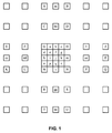
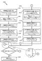
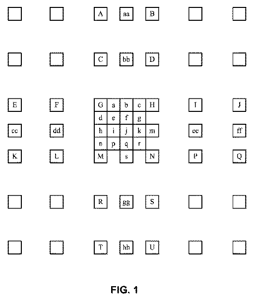
H.264のようなビデオ圧縮技法では、動き補償(MC)の精度は、たとえば、ルーマサンプル間の距離の1/4の単位である。動きベクトルが整数サンプル位置を指す例では、予測信号は、参照ピクチャの対応するサンプルからなる。動きベクトルが整数サンプル位置以外を指す例では、対応するサンプルは、非整数位置を生成するための補間を使用して取得される。1/2サンプル位置における予測値は、1次元の6タップ有限インパルス応答(FIR)フィルタを水平方向および垂直方向に適用することによって取得され得る。1/4サンプル位置における予測値は、整数位置および1/2サンプル位置におけるサンプルを平均することによって生成され得る。 In video compression techniques such as H.264, motion compensation (MC) accuracy is, for example, a unit of 1/4 of the distance between luma samples. In the example where the motion vector points to integer sample positions, the prediction signal consists of corresponding samples of the reference picture. In the example where the motion vector refers to something other than an integer sample position, the corresponding sample is obtained using interpolation to generate a non-integer position. Predicted values at 1/2 sample positions can be obtained by applying a one-dimensional 6-tap finite impulse response (FIR) filter in the horizontal and vertical directions. Predicted values at 1/4 sample positions can be generated by averaging samples at integer positions and 1/2 sample positions.
図1は、サンプルa-kおよびn-rに対する分数サンプル補間を示す。bおよびhと標識された1/2サンプル位置におけるサンプルは、それぞれ次のように6タップフィルタを適用することによって、中間値b1およびh1をまず計算することによって導出される。 FIG. 1 shows fractional sample interpolation for samples ak and nr. Samples at 1/2 sample positions labeled b and h are derived by first calculating intermediate values b 1 and h 1 by applying a 6-tap filter, respectively, as follows:
b1=(E-5F+20G+20H-5I+J) Eq. (1) b 1 = (E-5F + 20G + 20H-5I + J) Eq. (1)
h1=(A-5C+20G+20M-5R+T) Eq. (2) h 1 = (A-5C + 20G + 20M-5R + T) Eq. (2)
位置bおよびhに対する最終予測値は、次のように得られ、0〜255の範囲にとどめられ得る。 The final predicted values for positions b and h are obtained as follows and can be kept in the range 0-255.
b=(b1+16)>>5 Eq. (3) b = (b 1 +16) >> 5 Eq. (3)
h=(h1+16)>>5 Eq. (4) h = (h 1 +16) >> 5 Eq. (4)
jと標識された1/2サンプル位置におけるサンプルは、
j1=cc-5dd+20h1+20m1-5ee+ff Eq. (5)
によって得られてよく、cc、dd、ee、m1、およびffによって示される中間値は、h1と同様の方式で得られる。そして、最終予測値jは、
j=(j1+512)>>10 Eq. (6)
として計算され、0〜255nの範囲にとどめられ得る。
The sample at the 1/2 sample position labeled j is
j 1 = cc-5dd + 20h 1 + 20m 1 -5ee + ff Eq. (5)
The intermediate values indicated by cc, dd, ee, m 1 , and ff are obtained in the same manner as h 1 . And the final predicted value j is
j = (j 1 +512) >> 10 Eq. (6)
And can be kept in the range of 0-255n.
jの値を得る2つの代替的な方法は、フィルタリング動作が1/2サンプル位置の生成のために分離可能であることを示す。 Two alternative ways of obtaining the value of j indicate that the filtering operation is separable for the generation of 1/2 sample positions.
さらに図1を参照すると、a、c、d、n、f、i、k、およびqと標識された1/4サンプル位置におけるサンプルは、たとえば、
a=(G+b+1)>>1 Eq. (7)
として、整数サンプル位置および1/2サンプル位置における2つの最も近いサンプルの上方丸めを伴って平均することによって導出される。
Still referring to FIG. 1, samples at 1/4 sample positions labeled a, c, d, n, f, i, k, and q are, for example,
a = (G + b + 1) >> 1 Eq. (7)
As an average with the upper rounding of the two closest samples at the integer sample position and the 1/2 sample position.
e、g、p、およびrと標識された1/4サンプル位置におけるサンプルは、たとえば、
e=(b+h+1)>>1 Eq. (8)
として、対角方向にある1/2サンプル位置における最も近い2つのサンプルを上方丸めを伴って平均することによって導出される。
Samples at 1/4 sample locations labeled e, g, p, and r are, for example:
e = (b + h + 1) >> 1 Eq. (8)
Is derived by averaging the nearest two samples at half sample positions in the diagonal direction with upward rounding.
クロマ成分の予測値は、双線形補間によって得られ得る。クロマのサンプリング格子は、ルーマのサンプリング格子よりも分解能が低いので、クロマのために使用される変位は、1/8サンプル位置の精度を有する。 The predicted value of the chroma component can be obtained by bilinear interpolation. Since the chroma sampling grid has a lower resolution than the luma sampling grid, the displacement used for the chroma has an accuracy of 1/8 sample position.
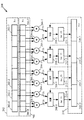
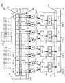
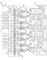
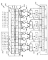
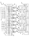
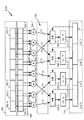
図2を参照すると、例示的なマルチタップ統合補間フィルタ200は、ピクセルウィンドウレジスタ202、乗算器のアレイ、この例では8個の乗算器204-0、204-1、…、204-7(総称的に「乗算器204」または「乗算器アレイ」と呼ばれ、「204」は図面に明確に現れない)、およびタップ係数セットレジスタ206を含む。ピクセルウィンドウレジスタは、複数の、この例では8個のピクセルレジスタ202-0、202-1、…、202-7(総称的に「202-x」と呼ばれ、これは図面には現れない)を有し得る。ある態様では、ピクセルウィンドウレジスタ202を形成する8個のピクセルレジスタ202-xは、パラレルにロード可能なように、パラレルな出力を有するように構成されてよく、たとえば、図2で右から左として示されるような「方向」に、バケツリレー方式で一緒に、選択的にシフトされるように構成され得る。代替的に、ある態様では、ピクセルレジスタ202-xは、ピクセルウィンドウレジスタ202が8ピクセルのパラレルイン/パラレルアウトシフトレジスタ機能を提供するように構成され得る。ピクセルレジスタ202-xは、Sビットの幅であり得る。限定されることなく、「S」の1つの例示的な値は8ビットである。ピクセルウィンドウレジスタ202の1つの例示的な実装形態は、パラレルなロードおよび出力という特徴を有する、ファーストインファーストアウト(FIFO)またはFIFOパイプラインであり得る。ピクセルウィンドウレジスタ202の具体的な構造に関して、自身の保有するノウハウを本開示に適用する当業者は、様々な構造的な実装形態を容易に特定することができるので、そのような構造のさらなる詳細な説明は省略される。
Referring to FIG. 2, an exemplary multi-tap integrated
より後のセクションでより詳細に説明されるように、ピクセルウィンドウレジスタ202を通るSビットのピクセルデータの「右から左への」シフトは、一部、畳み込みタイプの演算をもたらし得る。図3を参照して後のセクションで説明される一例は、ピクセルアレイの例示的な領域(図2には示されない)の行(図2には示されない)にわたる8個のピクセル(図2には示されない)を包含する、ウィンドウのシフトをもたらし得る。
As described in more detail in later sections, a “right-to-left” shift of S-bit pixel data through the
図2を続けて参照すると、いくつかの態様に対するさらなる動作を説明する際に図面を参照するときに便利なように、乗算器204-0および204-1は、代替的に「第1の乗算器ペア」204-0/1と呼ばれ、乗算器204-2および204-3は「第2の乗算器ペア」204-2/3と呼ばれ、乗算器204-4および204-5は「第3の乗算器ペア」204-4/5と呼ばれ、乗算器204-6および204-7は「第4の乗算器ペア」204-6/7と呼ばれる。「乗算器ペア」という用語は、いくつかの態様に関する例示的な動作を説明するためだけのものであり、ハードウェアアーキテクチャを定義することは意図されないことを理解されたい。逆に、より後のセクションにおけるさらに詳細な説明から理解されるように、一態様では、乗算器204の出力は、図2に示されるものとは異なる構成で、加算デバイス208-yに結合され得る。 Continuing to refer to FIG. 2, multipliers 204-0 and 204-1 are alternatively referred to as "first multiplication, as is convenient when referring to the drawings in describing further operations for some aspects. "Multiplier pair" 204-0 / 1, multipliers 204-2 and 204-3 are called "second multiplier pair" 204-2 / 3, and multipliers 204-4 and 204-5 are " The third multiplier pair "204-4 / 5" is referred to, and the multipliers 204-6 and 204-7 are referred to as "fourth multiplier pair" 204-6 / 7. It should be understood that the term “multiplier pair” is only for describing exemplary operations for some aspects and is not intended to define a hardware architecture. Conversely, as will be appreciated from a more detailed description in a later section, in one aspect, the output of multiplier 204 is coupled to summing device 208-y in a different configuration than that shown in FIG. obtain.
図2をさらに参照すると、ある態様では、乗算器204の各々は、上で説明されたピクセルレジスタ202-xの対応する1つに結合される、または結合されることが可能な第1のオペランドポート(示されているが別々に標識されてはいない)、および、タップ係数セットレジスタ206の対応するタップ係数レジスタ206-xに結合される、または結合されることが可能な第2のオペランドポート(示されているが別々には番号を付けられていない)によって構成され得る。ある態様では、タップ係数セットレジスタ206は、たとえば、第8のタップ係数レジスタ206-7で終わる、第1のタップ係数レジスタ206-0、第2のタップ係数レジスタペア206-1などを含み得る。
With further reference to FIG. 2, in an aspect, each of the multipliers 204 is coupled to or can be coupled to a corresponding one of the pixel registers 202-x described above. Port (shown but not separately labeled) and a second operand port that is or can be coupled to the corresponding tap coefficient register 206-x of the tap coefficient set register 206 (Shown but not numbered separately). In an aspect, the tap coefficient set
ある態様では、乗算器204は、固定小数点乗算を実行するように構成されてよく、このことは、例示的な演算を説明するために仮定される。しかし、この仮定は、概念とは関係のない複雑さをもたらすことなく例示的な処理の説明を容易にするためのものにすぎず、考慮される実施形態の範囲を限定することは意図されない。逆に、本開示を読めば、実施形態は浮動小数点の計算を使用して実施され得ることが、当業者により容易に理解されるだろう。 In an aspect, the multiplier 204 may be configured to perform fixed point multiplication, which is assumed to describe an exemplary operation. However, this assumption is merely to facilitate the description of the exemplary process without introducing complexity unrelated to the concept, and is not intended to limit the scope of the contemplated embodiments. Conversely, upon reading this disclosure, it will be readily appreciated by those skilled in the art that the embodiments may be implemented using floating point calculations.
図2をさらに参照すると、より後のセクションでより詳細に説明されるように、ある態様では、マルチタップ統合補間フィルタ200は、タップ係数の複数のセット(図2には特に示されていない)を記憶装置(図2には特に示されていない)に記憶し、タップ係数のそのようなセットを選択的に取り出し、これらをタップ係数セットレジスタ206にロードするように構成され得る。ピクセルウィンドウレジスタ202およびタップ係数セットレジスタ206は同一の構造を有してよく、たとえば、各々がレジスタアレイ(明確には示されていない)中の論理的に指定されたレジスタであり得ることを理解されたい。
With further reference to FIG. 2, as will be described in more detail in a later section, in one aspect, the multi-tap
図2をさらに参照すると、1つの構成では、第1の乗算器ペア204-0、204-1のそれぞれの出力は、第1の加算デバイス208-0のオペランド入力ポート(示されるが、別々には番号を付けられていない)、第2の加算デバイス208-1のオペランド入力ポート(示されるが、別々には番号を付けられていない)に入力する第2の乗算器ペア204-2、204-3のそれぞれの出力、第3の加算デバイス208-2のオペランド入力ポート(示されるが、別々には番号を付けられていない)に入力する第3の乗算器ペア204-4、204-5のそれぞれの出力、および、第4の加算デバイス208-3のオペランド入力ポート(示されるが、別々には番号を付けられていない)に入力する第4の乗算器ペア204-6、204-7のそれぞれの出力へと、スイッチングされ、ルーティングされ、または別様に結合され得る。例示的な動作の説明を簡潔にするために、第1の加算デバイス208-0、第2の加算デバイス208-1、第3の加算デバイス208-2、および第4の加算デバイス208-3はまた、総称的に、「加算デバイス208-y」として個々に呼ばれ、「加算デバイス208」としてまとめて呼ばれ、「208-y」および「208」という標識は図面には明確には現れないことを理解されたい。 Still referring to FIG. 2, in one configuration, the output of each of the first multiplier pair 204-0, 204-1 is connected to the operand input port of the first summing device 208-0 (shown separately, Are not numbered), a second multiplier pair 204-2, 204 that inputs to the operand input port of the second summing device 208-1 (not shown but separately numbered) -3 respective outputs, a third multiplier pair 204-4, 204-5 that inputs to an operand input port (not shown but separately numbered) of the third summing device 208-2 , And a fourth multiplier pair 204-6, 204-7 that inputs to an operand input port (not shown but separately numbered) of the fourth summing device 208-3 Can be switched, routed, or otherwise coupled to their respective outputs. To simplify the description of the exemplary operation, the first summing device 208-0, the second summing device 208-1, the third summing device 208-2, and the fourth summing device 208-3 are Also generically referred to individually as “adding device 208-y”, collectively referred to as “adding device 208”, and the signs “208-y” and “208” do not appear clearly in the drawing. Please understand that.
加算デバイス208への乗算器204の図示され説明される結合を実施するための、スイッチング、ルーティング、または結合の論理(図示されず)に関して、一態様では、当業者は、本開示に基づいて、従来のデジタルシグナルプロセッサの設計技法を適用することによってそのような論理を選択し、または別様に実装できるので、スイッチング、ルーティング、または結合の論理のさらなる詳細な説明は省略される。 With respect to switching, routing, or combination logic (not shown) to implement the illustrated and described combination of multipliers 204 to summing device 208, in one aspect, those skilled in the art, in accordance with the present disclosure, Since such logic can be selected or otherwise implemented by applying conventional digital signal processor design techniques, further detailed description of switching, routing, or coupling logic is omitted.
図2の参照を続けると、ある態様では、マルチタップ統合補間フィルタ200は、たとえば、4個の累算器レジスタ210-0、210-1、210-2、210-3(総称的に、「累算器レジスタ210-y」として個々に呼ばれ、「210-y」は図面には明確には現れないことが理解される)を有する累算器210を含み得る。4個という量は一例にすぎず、いかなる実施形態の範囲も限定することは意図されないことが理解されよう。累算器レジスタ210-0、210-1、210-2、および210-3は、別々に制御されるとは限らず、または別々に制御可能なレジスタであるとは限らず、代わりに、累算器210のフィールドであり得ることも理解されたい。さらに、累算器レジスタ210-0、210-1、210-2、および210-3は、4個のフィールドのサブセットとして、または、4個よりも多くのフィールドもしくはその等価物を有する実装された累算器210の等価物のサブセットとして実装され得ることが予想される。
Continuing to refer to FIG. 2, in one aspect, the multi-tap
図2をさらに参照すると、一態様では、各加算デバイス208の出力(示されるが、別々には番号を付けられていない)は、対応する累算器レジスタ210-yに直接入力し得る。さらなる態様では、図2のマルチタップ統合補間フィルタ200は、加算デバイス208の中の、またはそれと関連した、飽和論理、たとえば、図示された2Sビットの符号付き飽和論理212-0、212-1、212-2、212-3(まとめて「2Sビットの符号付き飽和論理212」と呼ばれ、総称的に「飽和論理」212-yとして個々に呼ばれ、「212」「212-y」という標識は図面に明確に現れないことを理解されたい)を含み得る。図2の本態様による例では、飽和論理212-yは、各加算デバイス208-yの出力(示されるが、別々には番号を付けられていない)と対応する累算器レジスタ210-yとの間に論理的に配置され得る。ここでの、および本明細書の他の例における「論理的に配置される」とは、「2Sビットの符号付き飽和論理」212-yが、別個のハードウェアまたは専用のハードウェアであるとは限らないことを意味し得ることを理解されたい。たとえば、一態様では、2Sビットの各符号付き飽和論理212-yは、プログラム可能な機能として、対応する加算デバイス208-yを実装する論理(別々には示されていない)へと組み込まれ得る。2Sビットの符号付き飽和論理212の具体的な構造に関して、当業者は、本開示に鑑みて、当業者に知られている標準的なデジタル設計技法および技術を本開示に適用することによって、そのような論理を実装するための技法および構造を容易に特定することができる。したがって、2Sビットの符号付き飽和論理212の構造のさらなる詳細な説明は省略される。
With further reference to FIG. 2, in one aspect, the output of each summing device 208 (shown but not separately numbered) may be input directly into the corresponding accumulator register 210-y. In a further aspect, the multi-tap
2Sビットの符号付き飽和論理212の動作および機能に関して、これらはさらに、8という以前に説明された例示的なSに関する例によって理解され、(この例では)ウィンドウレジスタ202が8ビットの符号なしのデータを保持し、タップ係数セットレジスタ206に記憶されるタップ係数データは符号付きの8ビットデータであることを意味する。したがって、この例では、2Sビットの符号付き飽和論理212の文脈における値「2S」は16に等しい。Sが8に等しく2Sが16に等しい、2Sビットの符号付き飽和論理212の例示的な特徴は、第1の乗算器ペア204-0、204-1、加算デバイス208-0、および2Sビットの符号付き飽和論理212-0を参照することによって理解され得る。より具体的には、乗算器204-0は、ピクセルレジスタ202-0からの8ビットの符号なしピクセルデータを、タップ係数レジスタ206-0からの対応する符号付きの8ビットのタップ係数と乗算し、1つの符号付きの16ビットの積を生成することができ、同様に、乗算器204-1は、ピクセルレジスタ202-1からの別の8ビットの符号なしピクセルデータを、タップ係数レジスタ206-1からの対応する符号付きの8ビットのタップ係数と乗算し、別の符号付きの16ビットの積を生成することができる。2つのそれぞれの符号付きの16ビットの積は、加算デバイス208-0の2つのオペランド入力ポート(示されるが、別々には番号を付けられていない)に入力される。ある態様では、第1の加算デバイス208-0は、たとえば、入力オペランドポート(示されるが、別々には番号を付けられていない)が累算器の第1のレジスタ210-0に結合されるのを可能にすることによって、または、論理(示されていない)が第1の加算デバイス208-0の内部にあることを可能にすることによって、累算器モードで動作するように選択的に構成され得る。第1の加算デバイス208-0は、累算器モードで動作するとき、符号付きの16ビットの積と、累算器の第1のレジスタ210-0の現在の内容とを加算(または符号によっては減算)することができ、積の合計の結果、または、累算された積の合計の結果を、2Sビットの符号付き飽和論理212-0に与えることができる。16ビットを超えると2Sビットの符号付き飽和論理212-0によって16ビットで飽和させられ得る、この積の合計の結果または累算された積の合計の結果が、次いで第1の累算器レジスタ210-0にロードされ得る。残りの乗算器204-2、204-3、…、204-7、および残りの加算デバイス208-1、208-2、および208-3は、ピクセルウィンドウレジスタ202からの対応するピクセルレジスタ202-xの内容およびタップ係数レジスタ206からのタップ係数レジスタ206-xの内容に対して同様に動作することができ、それぞれの16ビットの積の合計または累算された積の合計の結果を、残りの累算器レジスタ210-1、210-2、および210-3のうちの対応する1つに与えることができる。
With regard to the operation and function of the 2S bit signed saturation logic 212, these are further understood by the previously described example S example of 8 where (in this example) the
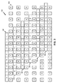
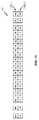
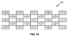
図3は、A、B、C、…、Mと標識された13個の画像ピクセルの行304に沿った位置の6回のステップシーケンスを通じた、ピクセルウィンドウ302のステップ移行のグラフィカルなモデル300を示す。ピクセルウィンドウ302は、8ビットの幅を有するものとして示されるが、これは単なる例であり、実施形態のいずれかの範囲を限定することは意図されない。開始位置302-0において、ピクセルウィンドウ302は、(8ピクセルという例示的な幅を仮定すると)ピクセルA、B、C、D、E、F、G、およびHにまたがり、終了位置302-5は、ピクセルF、G、H、I、J、K、L、およびMにまたがる。一態様では、6回のステップシーケンスは、3回の「偶数番目」のステップが3回の「奇数番目」のステップと交互に来るものと見なされ得る。「偶数番目」および「奇数番目」という標識は任意であることを理解されたい。関連する態様では、かつより後のセクションにおいてより詳細に説明されるように、図2のマルチタップ統合補間フィルタ200は、6個の状態または構成のシーケンスを通じて構成され操作されてよく、各状態は、シーケンス302-0、…、302-5における、ピクセルウィンドウ302の「偶数番目」または「奇数番目」のステップの1つに対応する。
FIG. 3 shows a
図2および図3を参照すると、図2のマルチタップ統合補間フィルタ200のピクセルウィンドウレジスタ202は、シーケンス302-0、…、302-5における図3のピクセルウィンドウ302のこれらの「偶数番目」または「奇数番目」のステップの各々において、その位置における図3のピクセルウィンドウ302がまたがるピクセルをロードされる。図2のマルチタップ統合補間フィルタ200は、一態様では、6個の図3のピクセルウィンドウ302の位置の各々において、1つまたは複数の例示的な実施形態に従って、補間フィルタプロセスを実行することができる。ある態様では、例示的な動作のより後の説明からさらに理解されるように、6個の図3のピクセルウィンドウ302の位置の各々において図2のマルチタップ統合補間フィルタ200によって実行される補間フィルタプロセスは、1つのマシンサイクルにおいて実行され得る。
With reference to FIGS. 2 and 3, the
「偶数番目」の図3のピクセルウィンドウ302の位置302-0、302-2、および302-4に対応する状態において図2のマルチタップ統合補間フィルタ200によって実行される例示的な補間フィルタプロセスを説明する際に便利なように、これらの例示的な補間フィルタプロセスは、代替的に「偶数番目」のマシンサイクルと呼ばれる。したがって、同様に、「奇数番目」の図3のピクセルウィンドウ302の位置302-1、302-3、および302-5に対応する状態においてマルチタップ統合補間フィルタ200によって実行される補間フィルタプロセスは、代替的に「奇数番目」のマシンサイクルと呼ばれる。
An exemplary interpolation filter process performed by the multi-tap
例示的な実施形態による方法およびシステムにおける1つの例示的な6ステップまたは6状態の短縮サイクル補間フィルタプロセスが、図2および図3とともに、図4、図5、図6、図7、図8、および図9を参照して以下でより詳細に説明される。概観すると、例は、図4を参照して説明されるような第1の「偶数番目」のマシンサイクルを含んでよく、このマシンサイクルにおいて、ピクセルウィンドウレジスタ202は、第1の「偶数番目」の位置302-0においてピクセルウィンドウ302がまたがり、第1のタップ係数セットをロードされたタップ係数セットレジスタ206による演算の対象となる、図3のピクセルをロードされ得る。この演算は、累算器210において、図3の4個の「偶数番目」の補間された1/2ピクセルa、c、e、およびgの初期値を生成し形成し得る。ある態様では、形成された4個の「偶数番目」の補間された1/2ピクセルa、c、e、およびgは、メモリ(図示されない)にオフロードされ得る。理解されるように、このオフロードは、そのいずれもが累算器210の使用について互いに干渉しない、「偶数番目」のマシンサイクルおよび「奇数番目」のマシンサイクルの交互配置を実現し得る。諒解されるように、この交互配置という特徴により、いくつかの利点の中でもとりわけ、様々な例示的な実施形態による実施において、統合補間フィルタが実現し得る。
One exemplary six-step or six-state shortened cycle interpolation filter process in the method and system according to the exemplary embodiment is illustrated in FIGS. 4, 5, 6, 7, 8, and 8 in conjunction with FIGS. And will be described in more detail below with reference to FIG. In overview, the example may include a first “even number” machine cycle as described with reference to FIG. 4, in which the
ある態様では、図5を参照したより詳細な説明からさらに理解されるように、第1の「奇数番目」のマシンサイクルにおいて、ピクセルウィンドウレジスタ202は、第1の「奇数番目」の位置302-1においてピクセルウィンドウ302がまたがるピクセルを保持するように更新されてよく、ピクセルウィンドウレジスタの内容は、第1の「偶数番目」のマシンサイクルのために使用される同じ第1のタップ係数セットを一態様では有するタップ係数セットレジスタ206による演算の対象となる。この演算は、ある態様では、図3の例示的な4個の「奇数番目」の1/2ピクセルb、d、f、およびhの初期値を形成することができ、これらは次いでメモリにオフロードされ得る。図6を参照してより詳細に説明されるように、第2の「偶数番目」のマシンサイクルは、前に形成された4個の「偶数番目」の補間された1/2ピクセルa、c、e、およびgによって累算器210をリロードするステップを含んでよく、ピクセルウィンドウレジスタ202は、第2の「偶数番目」の位置302-2においてピクセルウィンドウ302がまたがる図3のピクセルを有するように更新され、タップ係数セットレジスタ206は第2のタップ係数セットをロードされる。第2のタップ係数セットを有するタップ係数セットレジスタ206は次いで、図3の「偶数番目」の位置302-2を有するピクセルウィンドウレジスタ202の内容に対して演算を行い、増分の値(符号が正または負であり得る)を生成することができ、これらの増分の値は、累算器210において、前に形成された4個の「偶数番目」の補間された1/2ピクセルa、c、e、およびgを調整またはインクリメントすることができる。インクリメントされた4個の「偶数番目」の補間された1/2ピクセルa、c、e、およびgは、メモリにオフロードされ得る。
In some embodiments, as will be further understood from the more detailed description with reference to FIG. 5, in the first “odd-numbered” machine cycle, the
次に、図7を参照してより詳細に説明されるように、第2の「奇数番目」のマシンサイクルにおいて、累算器210は、前に形成された4個の「奇数番目」の補間された1/2ピクセルb、d、f、およびhをロードされてよく、ピクセルウィンドウレジスタ202は、第2の「奇数番目」の位置302-2においてピクセルウィンドウ302がまたがる図3のピクセルを有するように更新される。タップ係数セットレジスタセット206は、一態様では、第2のタップ係数セットを保持することができる。次いで、「偶数番目」の補間された1/2ピクセルa、c、e、およびgのインクリメントと同様の方式で、図3の「偶数番目」の位置302-2を有するピクセルウィンドウレジスタ202の内容は、タップ係数セットレジスタ206による演算の対象となり、増分の値を生成することができ、この増分の値は、累算器210において、前に形成された4個の「奇数番目」の補間された1/2ピクセルb、d、f、およびhを調整またはインクリメントすることができ、インクリメントされたピクセルは次いでメモリにオフロードされ得る。
Next, as described in more detail with reference to FIG. 7, in the second “odd-numbered” machine cycle, the
概観を続け、図8を参照してより詳細に説明されるように、第3の「偶数番目」のマシンサイクルは、前にインクリメントされた4個の「偶数番目」の補間された1/2ピクセルa、c、e、およびgを累算器210にリロードするステップ、第3の「偶数番目」の位置302-4においてピクセルウィンドウ302がまたがる図3のピクセルを有するようにピクセルウィンドウレジスタ202を更新するステップ、第3のタップ係数セットをタップ係数セットレジスタ206にロードするステップ、および、第2の「偶数番目」のマシンサイクルと実質的に同じ算術演算を使用して、4個の「偶数番目」の補間された1/2ピクセルa、c、e、およびgの最終値を累算器210において確立するステップを含み得る。同様に、図9を参照してより詳細に説明されるように、累算器210は、前にインクリメントされた4個の「奇数番目」の補間された1/2ピクセルb、d、f、およびhをリロードされてよく、ピクセルウィンドウレジスタ202は、第3の「奇数番目」の位置302-5においてピクセルウィンドウ302がまたがる図3のピクセルを有するように更新される。ある態様では、タップは、第3のタップ係数セットを保持することができ、増分の値は、4個の「奇数番目」の補間された1/2ピクセルb、d、f、およびhの最終値を累算器210において確立するために生成され得る。全体で3回の「偶数番目」のマシンサイクルの間に4個の「偶数番目」の補間された1/2ピクセルa、c、e、およびgを形成し累算することを、全体で3回の「奇数番目」のマシンサイクルの間に4個の「奇数番目」の補間された1/2ピクセルb、d、f、およびhを形成し累算することと交互に行うことによって、様々な例示的な実施形態による実施における統合補間フィルタは、8個の補間された1/2ピクセルa、b、c、d、e、f、g、およびhという完全なセットを、わずか6回のマシンサイクルで提供できることが、本開示を読めば当業者により諒解されるだろう。
Continuing the overview, as explained in more detail with reference to FIG. 8, the third “even” machine cycle is the four “even” interpolated 1/2 incremented previously. Reloading pixels a, c, e, and g into
例示的な実施形態による方法およびシステムにおける例示的な6状態の短縮サイクル補間フィルタプロセスが、ここで、図2および図3とともに、図4、図5、図6、図7、図8、および図9を参照して以下でより詳細に説明される。一態様では、第1の「偶数番目」のマシンサイクルおよび第1の「奇数番目」のマシンサイクルは、[1, -5, 1, -5, 1, -5, 1, -5]という第1のタップ係数セットを使用することができる。図面において、[1, -5, 1, -5, 1, -5, 1, -5]という第1のタップ係数セットは、図4および図5に現れるタップ係数セットレジスタ206のタップ係数セットレジスタ状態406として標識されている。1つの関連する態様では、タップ係数レジスタ206の図6および図7のタップ係数セットレジスタ状態606に反映されるように、第2のタップ係数セットは[20, 20, 20, 20, 20, 20, 20, 20]であってよく、1つのさらなる態様では、図8および図9のタップ係数セットレジスタ状態806に反映されるように、第3のタップ係数セットは[-5, 1, -5, 1, -5, 1, -5, 1]であってよい。これらは、第1、第2、および第3のタップ係数セットのそれぞれの値の例にすぎず、他の値が他の所望のフィルタ動作を得るために使用され得ることを理解されたい。実施形態は、2セットよりも多くのタップ係数を有することが考慮されることも理解されたい。
An exemplary six-state shortened cycle interpolation filter process in methods and systems according to exemplary embodiments is now illustrated in FIGS. 4, 5, 6, 7, 8, and 8 in conjunction with FIGS. This will be described in more detail below with reference to FIG. In one aspect, the first “even” machine cycle and the first “odd” machine cycle are numbered [1, -5, 1, -5, 1, -5, 1, -5]. A tap coefficient set of 1 can be used. In the drawings, the first tap coefficient set [1, -5, 1, -5, 1, -5, 1, -5] is the tap coefficient set register of the tap coefficient set
図4から図9のマシン状態において、図2のマルチタップ統合補間フィルタ200により示される例示的な算術演算を説明する前に、この説明は、様々なデータ経路に挿入される、または、様々な説明される論理および算術デバイス内に挿入される、ラッチ(図示されない)がないと仮定していることを理解されたい。言い換えれば、図2を参照すると、1つのマシンサイクルにおいて、ピクセルウィンドウレジスタ202からのピクセル値およびタップ係数セットレジスタ206の中のタップ係数値は、乗算器アレイ204に渡され、加算デバイス208および2Sビットの飽和論理212を通過し累算器210にロードされるそれぞれの積を形成するように乗算され得ることが仮定される。ラッチがないというこの仮定は、これらのデータ経路におけるラッチが原因のクロックサイクルの遅延を説明する必要を伴わずに例示的な動作を説明することが目的にすぎないことを理解されたい。しかし、当業者は、説明された概念を、たとえば、説明されたデータ経路におけるラッチを利用する実施に対して容易に適合させることができる。
Before describing the example arithmetic operations illustrated by the multi-tap
さらに、図3のシーケン302-0、…、302-5と、例示的な実施形態による実施におけるピクセルアレイにわたる他のピクセルウィンドウの移動とを繰り返す能力を有するピクセルウィンドウレジスタ202を実装し、タップ係数セットレジスタ206を実装するための、様々な技法および構造が、本開示から当業者には明らかとなるので、そのような技法および構造のさらなる詳細な説明は省略される。
In addition, a
例示的な実施形態による方法およびシステムにおける、例示的な6状態の短縮サイクル補間フィルタプロセスの、図4、図5、図6、図7、図8、および図9を参照した説明を簡単にする目的で、2Sビットの飽和論理212により実行される具体的な動作は省略される。本開示を読んだ当業者は、当業者が持つ固定小数点算術演算についての一般的なノウハウを開示される概念に適用して、中間の処理結果および最終的な1/2ピクセルの結果a、b、…、hを、所望の数値範囲内に維持することができる。したがって、主題の演算に付随する例を除いて、説明では、乗算および累算の演算によってもたらされる数値的な増大を無視する。 FIG. 4, FIG. 5, FIG. 6, FIG. 7, FIG. 8, and FIG. 9 are simplified descriptions of exemplary six-state shortened cycle interpolation filter processes in methods and systems according to exemplary embodiments. For purposes of illustration, the specific operations performed by the 2S bit saturation logic 212 are omitted. Those of ordinary skill in the art who have read this disclosure will apply their general know-how about fixed point arithmetic operations to the disclosed concepts to produce intermediate processing results and final half-pixel results a, b. ,..., H can be maintained within a desired numerical range. Thus, except for the examples associated with the subject operations, the description ignores the numerical increase caused by multiplication and accumulation operations.
図2から図4を参照すると、例示的な第1の「偶数番目」のマシンサイクルがより詳細に説明される。ある態様では、第1の「偶数番目」のマシンサイクルは、図4のピクセルウィンドウレジスタ202を状態402へとロードするステップと、図3のウィンドウ302の位置302-0がまたがるピクセルA、B、C、D、E、F、G、およびHを反映するステップと、タップ係数セットレジスタ206を、[1, -5, 1, -5, 1, -5, 1, -5]という第1のタップ係数セットである状態406へとロードするステップとを含み得る。乗算器204は、ピクセルウィンドウレジスタ202の状態402のピクセルA、B、C、D、E、F、Gを、タップ係数セットレジスタ206の状態406と乗算し、4個の積のペアを生成し、これらを、加算デバイス208の対応する1つのそれぞれのオペランドポート(示されるが標識されていない)に入力することができる。
With reference to FIGS. 2-4, an exemplary first “even” machine cycle is described in more detail. In one aspect, the first “even-numbered” machine cycle includes loading the
一態様では、乗算演算は、乗算器ペア204-0、204-1が、第1のピクセルレジスタ202-0および第2のピクセルレジスタ202-1からピクセルAおよびBを受け取り、これらのピクセルAおよびBをそれぞれ、[1, -5, 1, -5, 1, -5, 1, -5]という第1のタップ係数セットからの「1」および「-5」と乗算し、次いで、「A」および「-5B」であるそれぞれの積を、第1の加算デバイス208-0のオペランドポートに入力することを含み得る。第1の加算デバイス208-0の出力(A-5B)は、こうして、第1の累算器レジスタ210-0における「偶数番目」の補間された1/2ピクセルaを形成する。第2の乗算器ペア204-2、204-3は同様に、第3のピクセルレジスタ202-2および第4のピクセルレジスタ202-3から、それぞれピクセルCおよびDを受け取り、これらを、状態406における第3のタップ係数レジスタ206-2および第4のタップ係数レジスタ206-3から「1」および「-5」と乗算し、結果の出力である「C」および「-5D」を、第2の加算デバイス208-1の入力オペランドポートに送ることができる。第2の加算デバイス208-0の出力(C-5D)は、こうして、第2の累算器レジスタ210-1における「偶数番目」の補間された1/2ピクセルcを形成することができる。同様に、第3の乗算器ペア204-4、204-5は、第5のピクセルレジスタ202-4および第6のピクセルレジスタ202-5からピクセルEおよびFを受け取り、これらを、第5のタップ係数レジスタ206-4および第6のタップ係数レジスタ206-5からの「1」および「-5」と乗算して、第3の加算デバイス208-2を通じて、第3の累算器レジスタ210-2における「偶数番目」の補間された1/2ピクセルeを形成することができる。同様に、第4の乗算器ペア204-6、204-7は、第7のピクセルレジスタ202-6および第8のピクセルレジスタ202-7からピクセルGおよびHを受け取り、これらを、第7のタップ係数レジスタ206-6および第8のタップ係数レジスタ206-7からの「1」および「-5」と乗算して、第4の加算デバイス208-3を通じて、第4の累算器レジスタ210-3における「偶数番目」の補間された1/2ピクセルgを形成することができる。 In one aspect, the multiplication operation is such that multiplier pair 204-0, 204-1 receives pixels A and B from first pixel register 202-0 and second pixel register 202-1, and these pixels A and Each B is multiplied by "1" and "-5" from the first set of tap coefficients [1, -5, 1, -5, 1, -5, 1, -5], then "A And “−5B” may be input to the operand ports of the first summing device 208-0. The output (A-5B) of the first summing device 208-0 thus forms the "even number" interpolated 1/2 pixel a in the first accumulator register 210-0. The second multiplier pair 204-2, 204-3 similarly receives pixels C and D from the third pixel register 202-2 and the fourth pixel register 202-3, respectively, Multiplies "1" and "-5" from the third tap coefficient register 206-2 and fourth tap coefficient register 206-3, and outputs the resulting outputs "C" and "-5D" to the second Can be sent to the input operand port of summing device 208-1. The output (C-5D) of the second summing device 208-0 can thus form an “even number” interpolated half pixel c in the second accumulator register 210-1. Similarly, the third multiplier pair 204-4, 204-5 receives pixels E and F from the fifth pixel register 202-4 and the sixth pixel register 202-5, and inputs them to the fifth tap. Multiply by "1" and "-5" from coefficient register 206-4 and sixth tap coefficient register 206-5 and through third adder device 208-2, third accumulator register 210-2 The “even-numbered” interpolated half-pixel e in can be formed. Similarly, the fourth multiplier pair 204-6, 204-7 receives the pixels G and H from the seventh pixel register 202-6 and the eighth pixel register 202-7 and converts them to the seventh tap. Multiply by "1" and "-5" from coefficient register 206-6 and eighth tap coefficient register 206-7, and through fourth adder device 208-3, fourth accumulator register 210-3 The “even-numbered” interpolated half-pixel g in can be formed.
したがって、累算器210の内容410は、この例では第1の「偶数番目」のマシンサイクルの終わりにおいて、図4の領域470において示される「偶数番目」の補間された1/2ピクセルa、c、e、gの中間値を有し得る。ある態様では、領域470において示される値を伴う説明された補間された1/2ピクセルa、c、e、gを有する内容410は、メモリにオフロードされ得る。
Accordingly, the
ここで図3および図5を参照すると、第1の「奇数番目」のマシンサイクルの例示的なプロセスが説明される。一態様では、図2のピクセルウィンドウレジスタ202は、B、C、D、E、F、G、H、Iである図3の第2のピクセルウィンドウ位置302-1に対応するピクセルを包含するように、ピクセルの内容を1ピクセル左にシフトする。これは、図5のピクセルウィンドウレジスタの状態502において反映されており、ピクセル「I」をシフトする最後のピクセルレジスタ202-7のファーストインファーストアウト(FIFO)動作によって実行されてよく、x=0〜6に対して、ピクセルレジスタ202-xの各々は、(右から左の順で)先行するピクセルレジスタ202-x+1の内容を受け取る。タップ係数セットレジスタ206の内容は状態406のまま、すなわち、[1, -5, 1, -5, 1, -5, 1, -5]という第1のタップ係数セットのままである。ある態様では、乗算器204および加算デバイス208は、タップ係数レジスタ206の状態406、すなわち、[1, -5, 1, -5, 1, -5, 1, -5]という第1のタップ係数セットを、第1の「偶数番目」のサイクルについて説明されたのと同じ方式で、ピクセルB、C、D、E、F、G、Hと乗算して、加算デバイス20を通じて、累算器210において、以下の4個の「奇数番目」の補間された1/2ピクセルb、d、f、およびh、すなわち、第1の累算器レジスタ210-0における補間された1/2ピクセルbの初期値として(B-5C)、第2の累算器レジスタ210-1における補間された1/2ピクセルdの初期値として(D-5E)、第3の累算器レジスタ210-2における補間された1/2ピクセルfの初期値として(F-5G)、および第4の累算器レジスタ210-3における補間された1/2ピクセルhの初期値として(H-5I)を形成する。累算器210の内容510、すなわち、「奇数番目」の補間された1/2ピクセルb、d、f、およびhの初期値が、図5の領域572において示され、ある態様では、メモリにオフロードされ得る。
Referring now to FIGS. 3 and 5, an exemplary process of the first “odd number” machine cycle is described. In one aspect, the
ここで図3および図6を参照すると、例示的な第2の「偶数番目」のマシンサイクルでは、第1の「偶数番目」のマシンサイクルにおいて形成された4個の「偶数番目」の補間された1/2ピクセルa、c、e、およびgの初期値は、基本的には、第1の「偶数番目」のマシンサイクルの演算を繰り返すことによって、しかし、図3の第3のピクセルウィンドウ位置302-2におけるピクセルおよび第2のタップ係数セット[20, 20, 20, 20, 20, 20, 20, 20]を使用して、かつ、前の4個の「偶数番目」の補間された1/2ピクセルa、c、e、およびgをインクリメントするためにその結果を使用することによって、インクリメントされ得る。 Referring now to FIGS. 3 and 6, an exemplary second “even” machine cycle is the four “even” interpolations formed in the first “even” machine cycle. The initial values of 1/2 pixels a, c, e, and g are basically by repeating the operation of the first “even” machine cycle, but the third pixel window of FIG. Using the pixel at location 302-2 and the second set of tap coefficients [20, 20, 20, 20, 20, 20, 20, 20] and the previous 4 “even” interpolated Can be incremented by using the result to increment half pixels a, c, e, and g.
図3および図6をさらに参照すると、ある態様では、第2の「偶数番目」のマシンサイクルは、前に形成された4個の「偶数番目」の補間された1/2ピクセルa、c、e、およびgを累算器210へとリロードするステップと、ピクセルウィンドウレジスタ202を、たとえばFIFO動作によって、ピクセルC、D、E、F、G、H、I、およびJを有するピクセルウィンドウレジスタの状態602へとシフトするステップと、状態606に反映されるように、例示的な第2のタップ係数セット[20, 20, 20, 20, 20, 20, 20, 20]をタップ係数セットレジスタ206にロードするステップとを含み得る。乗算器204は、タップ係数セットレジスタ206の内容または状態606[20, 20, 20, 20, 20, 20, 20, 20]を、ピクセルウィンドウレジスタ202の中のピクセルC、D、E、F、G、H、I、およびJと乗算し、得られた積を加算デバイス208と結合することができる。これらの乗算器204の出力および前に形成された4個の「偶数番目」の補間された1/2ピクセルa、c、e、およびgの図6に示されるフィードバックを受け取ることによって、加算デバイス208は、図6の領域672において示される以下の値を有する、インクリメントされた「偶数番目」の1/2ピクセルa、c、e、およびgを累算器210において形成することができる。それらの値は、第1の累算器レジスタ210-0における、(A - 5B + 20C + 20D)に等しいインクリメントされた「偶数番目」の補間された1/2ピクセルa、第2の累算器レジスタ210-1における、(C - 5D + 20E + 20F)に等しいインクリメントされた「偶数番目」の補間された1/2ピクセルc、第3の累算器レジスタ210-2における、(E - 5F + 20G+ 20H)に等しいインクリメントされた「偶数番目」の補間された1/2ピクセルe、および、第4の累算器レジスタ210-3における、(G - 5H + 20I + 20J)に等しいインクリメントされた「偶数番目」の補間された1/2ピクセルgである。ある態様では、これらのインクリメントされた4個の「偶数番目」の補間された1/2ピクセルa、c、e、およびgは、メモリにオフロードされ得る。
With further reference to FIGS. 3 and 6, in one aspect, the second “even” machine cycle includes the four “even” interpolated half-pixels a, c, reloading e and g into the
ここで、図3および図7を参照すると、例示的な第2の「奇数番目」のマシンサイクルにおいて、第1の「奇数番目」のマシンサイクルにおいて形成される4個の「奇数番目」の補間された1/2ピクセルb、d、f、およびhの初期値は、第2の「偶数番目」のマシンサイクルの演算を繰り返し、しかし、図3の第4のピクセルウィンドウ位置302-3におけるピクセルを使用することによって得られる結果により、インクリメントされる。タップ係数レジスタは、第2のタップ係数セット[20, 20, 20, 20, 20, 20, 20, 20]である状態606のままであり得る。ある態様では、ピクセルウィンドウレジスタ202は、図7のピクセルウィンドウレジスタの状態702によって示されるように、D、E、F、G、H、I、J、およびKである、図3の第4のピクセルウィンドウ位置302-3に対応するピクセルを包含するようにシフトされてよく、4個の「奇数番目」の補間された1/2ピクセルb、d、f、およびhの初期値をメモリから累算器210へとリロードする。一態様では、第2の「偶数番目」のマシンサイクルについて説明されたのと実質的に同じ演算で、第2の「奇数番目」のマシンサイクルは、累算器210の内容を、図7の領域772にも示される、「奇数番目」の補間された1/2ピクセルb、d、f、およびhの以下の値へと更新することができる。それらの値は、第1の累算器レジスタ210-0における、(B - 5C + 20D + 20E)に等しいインクリメントされた「奇数番目」の補間された1/2ピクセルb、第2の累算器レジスタ210-1における、(D - 5E + 20F + 20G)に等しいインクリメントされた「奇数番目」の補間された1/2ピクセルd、第3の累算器レジスタ210-2における、(F - 5G + 20H + 20I)に等しいインクリメントされた「奇数番目」の補間された1/2ピクセルf、および、第4の累算器レジスタ210-3における、(H - 5I + 20J + 20K)に等しいインクリメントされた「奇数番目」の補間された1/2ピクセルhである。ある態様では、これらのインクリメントされた4個の「奇数番目」の補間された1/2ピクセルb、d、f、およびhは、メモリにオフロードされ得る。
Referring now to FIGS. 3 and 7, in the exemplary second “odd number” machine cycle, four “odd number” interpolations formed in the first “odd number” machine cycle. The initial values of the half-pixels b, d, f, and h repeated the operation of the second “even” machine cycle, but the pixel at the fourth pixel window location 302-3 in FIG. Is incremented by the result obtained by using. The tap coefficient register may remain in
ここで、図3および図8を参照すると、一態様では、第3の「偶数番目」のマシンサイクルは、第2の「偶数番目」のマシンサイクルの演算を繰り返すことによって得られる結果を使用して、ただし、図3の第5のピクセルウィンドウ位置302-4のピクセルE、F、G、H、I、J、K、およびLを包含するようにピクセルウィンドウレジスタ202が状態802にシフトされ、第3のタップ係数セット[-5, 1, -5, 1, -5, 1, -5, 1]である状態806へと係数レジスタ206がロードされた状態で、(上で説明された第2の「偶数番目」のマシンサイクルによって)以前にインクリメントされた、4個の「偶数番目」の補間された1/2ピクセルa、c、e、およびgの値を、最終値へとインクリメントすることができる。ある態様では、以前にインクリメントされた4個の「偶数番目」の補間された1/2ピクセルa、c、e、およびgは、メモリから累算器210にロードされてよく、第2の「偶数番目」のマシンサイクルについて説明されたのと実質的に同じ演算で、第3の「偶数番目」のマシンサイクルは、累算器210の内容を、「偶数番目」の1/2ピクセルa、c、e、およびgの以下の最終値へと更新することができる。それらの最終値は、第1の累算器レジスタ210-0における、(A - 5B + 20C + 20D - 5E + F)に等しい「偶数番目」の補間された1/2ピクセルa、第2の累算器レジスタ210-1における、(C - 5D + 20E + 20F- 5G + H)に等しい「偶数番目」の補間された1/2ピクセルc、第3の累算器レジスタ210-2における、(E - 5F + 20G + 20H - 5I + J)に等しい「偶数番目」の補間された1/2ピクセルe、および、第4の累算器レジスタ210-3における、(G - 5H + 20I + 20J - 5K + L)に等しい「偶数番目」の補間された1/2ピクセルgである。これらの値は、図8の領域872において示される。
Referring now to FIGS. 3 and 8, in one aspect, the third “even number” machine cycle uses the result obtained by repeating the operation of the second “even number” machine cycle. However, the
ここで、図3および図9を参照すると、一態様では、第3の「奇数番目」のマシンサイクルは、第2の「偶数番目」のマシンサイクルの演算を繰り返すことによって得られる結果を使用して、ただし、図3の第6のピクセルウィンドウ位置302-5のピクセルE、F、G、H、I、J、K、およびMを包含するようにピクセルウィンドウレジスタ202が状態902にシフトされ、図9の領域972において示される以下の値を有する最終的な「奇数番目」の1/2ピクセルb、d、f、およびhを累算器210において形成する状態で、(上で説明された第2の「奇数番目」のマシンサイクルによって)以前にインクリメントされた、4個の「奇数番目」の補間された1/2ピクセルb、d、f、およびhの値を、最終値へとインクリメントすることができる。上記の値は、第1の累算器レジスタ210-0における(B - 5C + 20D + 20E - 5F + G)に等しい「奇数番目」の補間された1/2ピクセルb、第2の累算器レジスタ210-1における、(D - 5E + 20F + 20G - 5H + I)に等しい「奇数番目」の補間された1/2ピクセルd、第3の累算器レジスタ210-2における、(F - 5G + 20H + 20I - 5J + K)に等しい「奇数番目」の補間された1/2ピクセルf、および、第4の累算器レジスタ210-3における、(H - 5I + 20J + 20K - 5L + M)に等しい「奇数番目」の補間された1/2ピクセルhである。
Referring now to FIGS. 3 and 9, in one aspect, the third “odd” machine cycle uses the result obtained by repeating the operation of the second “even” machine cycle. However, the
図2のマルチタップ統合補間フィルタ200は、「偶数番目」および「奇数番目」の補間された1/2ピクセルの上で説明された例示的なセットを生成する際に、6タップの補間フィルタプロセスを実行したことを諒解されたい。6タップの補間フィルタは例にすぎず、任意の実施形態より包含される、または任意の実施形態の実施であり得る、実施および構造の範囲を限定することは意図されないことを理解されたい。たとえば、当業者は、6タップの補間フィルタに関して示された概念を容易に適用して、8タップの補間フィルタを実現することができる。
The multi-tap
図10は、様々な例示的な実施形態による、1つまたは複数の方法およびシステムにおける、短縮マシンサイクルサブピクセル補間の1つのプロセス1000の1つの例示的な論理フローを示す。1つの例示的な動作では、プロセス1000は、1002を経ることで開始してよく、または1002を経ることを含んでよく、ピクセルに割当てられたインデックス(図示されず)に対する「偶数番目」の位置に対応するピクセルを、ピクセルウィンドウレジスタにロードすることができ、または別様にそのピクセルによってピクセルウィンドウレジスタを設定することができる。たとえば、図3の位置302-0は、1002による「偶数番目」の位置の例であり得る。1つの例示的な動作において、プロセス1000は、1002に対して任意の時間において、しかし好ましくは1006よりも前に、1004において、タップ係数セットをタップ係数レジスタにロードすることができ、または別様にタップ係数セットによってタップ係数レジスタを確立することができる。図4を参照すると、様々な例示的な実施形態による実施について、1004においてタップ係数レジスタにタップ係数セットをロードするステップの一例は、たとえば、第1のタップ係数セット[1, -5, 1, -5, 1, -5, 1]によって、タップ係数セットレジスタ206を状態406へとロードまたは設定するステップであり得る。
FIG. 10 illustrates one example logic flow of one
図10を参照すると、ある態様の1つの例示的な動作において、プロセス1000は、好ましくは、1002および1004に対応する状態が確立された状態で、1006へ進み、様々な例示的な実施形態による補間マルチタップの「偶数番目」のマシンサイクルによって、「偶数番目」のサブピクセルのセットを形成することができる。様々な例示的な実施形態による、補間マルチタップフィルタの「偶数番目」のマシンサイクルによって「偶数番目」のサブピクセルのセットを形成するステップ1006の一例は、「偶数番目」の補間された1/2ピクセルa、c、e、およびgを形成するための、図4に関して説明された第1の「偶数番目」のマシンサイクルであり得る。
Referring to FIG. 10, in one exemplary operation of an aspect, the
図10の参照を続けると、1つの例示的な動作において、プロセス1000は、様々な例示的な実施形態による補間マルチタップフィルタの「偶数番目」のマシンサイクルによって「偶数番目」のサブピクセルのセットを形成するステップ1006の後で、1008へ進み、たとえば、1002における「偶数番目」の位置と関連付けられるインデックスに対する「奇数番目」の位置に対応するピクセルによって、ピクセルウィンドウレジスタの内容をシフトし、または別様に更新することができる。図3を参照すると、位置302-1は、1008による「奇数番目」の位置の一例を示す。ある態様では、1つの例示的な動作において、プロセス1000は、好ましくは、ピクセルウィンドウレジスタ状態が1008に対応しタップ係数レジスタが状態1004と関連付けられる状態で、1010へと進み、1つまたは複数の例示的な実施形態による補間マルチタップフィルタの「奇数番目」のマシンサイクルによって、「奇数番目」のサブピクセルのセットを形成することができる。補間マルチタップフィルタの「奇数番目」のマシンサイクルによって「奇数番目」のサブピクセルのセットを形成するステップ1010の一例は、「奇数番目」の補間された1/2ピクセルb、d、f、およびhを形成する、図5に関して説明された第1の「奇数番目」のマシンサイクルであり得る。
Continuing with reference to FIG. 10, in one exemplary operation, the
図10の参照を続けると、「オプション2」として表される論理フローを有するある態様では、プロセス1000に従った例示的な動作は、「奇数番目」の補間された1/2ピクセルb、d、f、およびhのセットを形成するステップ1010の後で、終了条件脱出ブロック1012へ進み、短縮マシンサイクルのサブピクセル補間に対する所与の終了条件が満たされているかどうかを判定することができる。言い換えれば、「オプション2」として表される論理フローを有する態様では、4個の「偶数番目」の補間された1/2ピクセルa、c、e、およびgと4個の「奇数番目」の補間された1/2ピクセルb、d、f、およびhとの上で説明された形成は、算術演算の全体を含んでよく、言い換えれば、8個の補間された1/2ピクセルa、b、c、d、e、f、g、およびhの完全なセットの最終値を生成することができる。この「オプション2」の態様は、各々が2個の積の合計である、完全なセットの最終的な補間された1/2ピクセルa、b、c、d、e、f、g、およびhの、2マシンサイクルによる生成を実現することができる。本態様による動作では、終了条件脱出ブロック1012のこの第1の例における答は「YES」であり、プロセス1000はブロック1014へ進み、補間された1/2ピクセルa、b、c、d、e、f、g、およびhの形成されたセットを出力することができる。
Continuing to refer to FIG. 10, in one aspect with a logic flow represented as “
図10についてさらに続けると、「オプション1」として表される論理フローを有する別の態様では、終了条件脱出ブロック1012は、奇数番目の補間された1/2ピクセルを形成するステップ1010の直後に終了条件脱出ブロック1012に入るのではなく、代わりに累算するステップ1050へ進むように構成され得る。以下でより詳細に説明されるように、オプション1では、終了条件脱出ブロック1012の終了条件は、1006および1010において形成されたサブピクセルの「偶数番目」のセットおよび「奇数番目」のセットを累算するステップ1050を繰り返した回数であり得る。
Continuing with FIG. 10, in another aspect having a logic flow represented as “
1つの例示的な動作では、「オプション1」の態様により構成されるプロセス1000の累算するステップ1050の第1の例は、1014において、別の「偶数番目」の位置に対応するピクセルによって、ピクセルウィンドウレジスタ(たとえば、図2のピクセルウィンドウレジスタ202)の内容をシフトし、または別様に更新するステップ、および、タップ係数の別のセットをタップ係数レジスタにロードし、または、そのセットによってタップ係数レジスタを別様に更新するステップであり得る。図3を参照すると、位置302-2は、1014による別の「偶数番目」の位置の一例を示す。図4を参照すると、たとえば、第2のタップ係数セット[20, 20, 20, 20, 20, 20, 20, 20]によって、図4のタップ係数セットレジスタ206を状態606へとロードまたは設定するステップは、1014の、別のタップ係数セットをタップ係数セットレジスタにロードするステップ、または別のタップ係数セットによってタップ係数レジスタを別様に更新するステップの一例を示す。図4のピクセルウィンドウレジスタ202の状態402はまた、1014における、「偶数番目」の位置の上で説明された図3の例示的な位置302-2を反映する。
In one exemplary operation, the first example of the accumulating
図10の参照を続けると、ある態様では、「偶数番目」のピクセルウィンドウレジスタの状態およびタップ係数レジスタの状態が1014における更新に従う、繰り返し累算する態様による1つの例示的な動作では、プロセス1000は、1016へ進み、1006において形成された、または、以下でより詳細に説明されるように、ループ1014、1016、1018、1020、および1112の先行する繰り返しによって以前にインクリメントされた、「偶数番目」のサブピクセルのセットを、インクリメントまたは別様に更新することができる。ここで説明される例では、これは、1014の第1の例であるので、インクリメントするステップは、1006において形成される「偶数番目」のサブピクセルのセットに対して行われる。補間マルチタップフィルタの「偶数番目」のマシンサイクルによって「偶数番目」のサブピクセルのセットをインクリメントする、または別様に更新するステップ1016の一例は、「偶数番目」の補間された1/2ピクセルa、c、e、およびgをインクリメントするための、図6に関して説明された第2の「偶数番目」のマシンサイクルであり得る。
Continuing with reference to FIG. 10, in one aspect, in one exemplary operation according to the iterative accumulation aspect, the state of the “even number” pixel window register and the state of the tap coefficient register are in accordance with the update at 1014. Goes to 1016 and is formed at 1006 or previously incremented by a previous iteration of
図10をさらに参照すると、プロセス1000の1つの例示的な動作において、プロセス1000は、補間マルチタップフィルタの「偶数番目」のマシンサイクルによって「偶数番目」のサブピクセルのセットをインクリメントするステップ1016の後で、1018へ進み、たとえば、1002および1014における「偶数番目」の位置と関連付けられるインデックスに対する別の「奇数番目」の位置に対応するピクセルによって、ピクセルウィンドウレジスタの内容をシフトし、または別様に更新することができる。たとえば、図3の位置302-3は、1018による「奇数番目」の位置の例であり得る。一態様によれば、例示的な動作において、プロセス1000は、「奇数番目」のピクセルウィンドウレジスタの状態が1018に対応し、同じタップ係数レジスタの状態が1016における「偶数番目」の更新において使用される状態で、1020へと進み、「奇数番目」のサブピクセルのセットをインクリメントし、または別様に更新することができる。これを、1020におけるインクリメントするステップまたは更新するステップの第1の例であると仮定すると、基本的な「奇数番目」のサブピクセルは1010において形成されたセットであり得る。累算するステップ150の次の繰り返しにおいて、基本的な「奇数番目」のサブピクセルは、終了条件脱出ブロック1012によるループとして形成される、累算するステップ、すなわち1014、1016、1018、1020の先行する繰り返しによって以前にインクリメントされたセットであることを理解されたい。補間マルチタップフィルタの「奇数番目」のマシンサイクルによって「奇数番目」の補間されたサブピクセルのセットをインクリメントする、または別様に更新するステップ1020の一例は、「奇数番目」の補間された1/2ピクセルb、d、f、およびhをインクリメントするための、図7に関して説明された第2の「奇数番目」のマシンサイクルであり得る。
Still referring to FIG. 10, in one exemplary operation of the
図10の参照を続けると、1つの例示的な動作において、プロセス1000は、補間マルチタップフィルタの「奇数番目」のマシンサイクルによって、「奇数番目」のサブピクセルのセットをインクリメントするステップ1020の後で、終了条件脱出ブロック1040へ進み、所与の終了条件、この態様では累算するステップ1050を繰り返した所与の回数が満たされたかどうかを判定することができる。図10とともに図8および図9を参照して以下でさらに詳細に説明される1つのそのような例は、この例では図8の第2の「偶数番目」のマシンサイクルによるものである「偶数番目」の補間された1/2ピクセルa、c、e、およびgの例示的な第2のインクリメントおよび最後のインクリメントを実行するステップ、および、この例では図9の第2の「奇数番目」のマシンサイクルによるものである「奇数番目」の補間された1/2ピクセルb、d、f、およびhの例示的な第2のインクリメントおよび最後のインクリメントを実行するステップである。
Continuing with reference to FIG. 10, in one exemplary operation, the
図10をさらに参照すると、この例では、所与の終了条件は、累算するステップ1050の2回以上の繰り返しであるので、終了条件脱出ブロック1012における答は「NO」であることが仮定される。したがって、プロセス1000は、累算するステップ1050に戻る。1014、1016、1018、1020、1012のループは、終了条件脱出ブロック1012における終了条件が満たされるまで続く。図8および図9を参照して説明される例を参照すると、これらは、1014、1016、1018、および1020の累算するステップ1050のループの繰り返しの一例を示す。終了条件脱出ブロック1012における終了条件が満たされると、サブピクセルを累算するステップ1050は完了し、プロセス1000は1014へ進み、最終的な補間されたサブピクセルを出力することができる。図8および図9を参照すると、最終的な補間されたサブピクセルを出力する1つの例示的なステップ1014は、サブピクセルa、b、c、d、e、f、g、およびhの最終値の説明された生成である。
Still referring to FIG. 10, in this example, it is assumed that the answer in the
図11は、一例として、1つの例示的な実施形態の2つピクセル行セクション1102_0および1102_1による、短縮サイクルマルチタップ補間フィルタ装置およびフィルタ方法において処理され得る入力1100を示す。「全体の」ピクセル0A、0B、0C、0D、0E、0F、0G、0H、0I、0J、0K、0L、および0M(まとめて「ピクセル0A〜0M」)を有するピクセル行セクション1102_0が示され、「全体の」ピクセル1A、1B、1C、1D、1E、1F、1G、1H、1I、1J、1K、1L、および1M(まとめて「ピクセル1A〜1M」)を有するピクセル行セクション1102_1が示される。例示的な実施形態による例示的なプロセスを説明する際、ピクセル0A〜0Mおよび1A〜1Mは、所与の値、たとえば、限定はされないが、光検出器(図示されない)の出力またはフィルタリングされた出力を有することが仮定される。しかし、語句「ピクセル行セクション」の中の「行」という用語は、ピクセルが行対列のビデオアレイの「行」に由来しなければならないことを必ずしも意味しないことを理解されたい。たとえば、ピクセル行セクション1102_0および1102_1は、アレイの隣接する、または別様に間隔を空けられた「列」(図示されない)、アレイの隣接する対角方向(図示されない)、またはアレイの他のそれぞれの領域に由来するものであってよい。
FIG. 11 shows, by way of example, an
図11の参照を続けると、1/2ピクセル位置0a、0b、0c、0d、0e、0f、0g、および0h(まとめて「1/2ピクセル0a〜0h」)を有するピクセル行セクション1102_0も示され、同様に、1/2ピクセル位置1a、1b、1c、1d、1e、1f、1g、および1h(まとめて「1/2ピクセル1a〜1h」)を有するピクセル行セクション1102_1が示される。
Continuing with reference to FIG. 11, also shown is a pixel row section 1102_0 with 1/2 pixel positions 0a, 0b, 0c, 0d, 0e, 0f, 0g, and 0h (collectively “1/2 pixels 0a-0h”). Similarly, a pixel row section 1102_1 having 1/2
付録Aを参照すると、擬似コードセクションA1は、1つの例示的な実施形態による、短縮サイクルマルチタップ補間フィルタ装置およびフィルタ方法のための、かつ、例示的なピクセル行102_0のピクセル0A〜0Mおよびピクセル行102_1のピクセル1A〜1Mを使用して、1つまたは複数の例示的な実施形態による、1/2ピクセル0a〜0hおよび1/2ピクセル1a〜1hを生成する際の演算のための、例示的なコンピュータ実行可能命令を示す。
Referring to Appendix A, pseudo-code section A1 includes pixels 0A-0M and pixels for an exemplary pixel row 102_0 for a shortened cycle multi-tap interpolation filter apparatus and filter method, according to one exemplary embodiment. Example for operations in generating 1/2 pixels 0a-0h and 1/2 pixels 1a-1h according to one or more exemplary
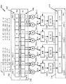
図12は、1つの例示的な実施形態による、図2の短縮サイクルマルチタップ補間フィルタ200の、インターリーブされたクロマ成分の構成1200の1つの双線形補間を示す。図12を参照すると、ある態様では、インターリーブされたクロマ成分の構成1200は、Rssレジスタ202の中の8個の8ビットの符号付きバイトを、Rttレジスタ206の中の対応する8ビットの符号なしのバイトと乗算することができ、乗算器204から加算デバイス208に向けられた矢印により示されるような交差するペアにおける乗算結果を加算する方式で、加算デバイス208-0、208-1、208-2、および208-3を構成する。図2と図12を比較すると、乗算器204から加算デバイス208への乗算結果のそれぞれのルーティングまたは結合は、様々な説明される動作に従ったものであることが諒解されるだろう。図2と図12との間で、加算デバイス208への乗算器204の結合のモードを変更するための、スイッチング、ルーティング、または結合の論理(図示されず)のための技法に関して、一態様では、当業者は、本開示に基づいて、従来のデジタルシグナルプロセッサの設計技法を適用することによってそのような論理を選択し、または別様に実装できるので、さらなる詳細な説明は省略される。
FIG. 12 illustrates one bilinear interpolation of the interleaved
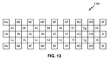
図13は、1つの例示的な実施形態による、平面的なクロマ成分の双線形補間に関与し得る、1つの例示的なピクセルのアレイ1300を示す。
FIG. 13 shows one exemplary array of
図14は、図13の例示的なアレイ1300に基づく、平面的なクロマ成分の双線形補間において生成される1/4ピクセルを有する、1つの例示的なピクセルのアレイ1400を示す。
FIG. 14 shows one exemplary array of
付録Aを参照すると、擬似コードセクションA2は、図13および図14を参照して、1つまたは複数の例示的な実施形態による装置および方法における、平面的なクロマ成分の双線形補間において1/4ピクセルを生成するためのコンピュータ実行可能命令の例を示す。 Referring to Appendix A, pseudo-code section A2 is described with reference to FIGS. 13 and 14, in a bilinear interpolation of planar chroma components in an apparatus and method according to one or more exemplary embodiments. Fig. 3 shows an example of computer executable instructions for generating 4 pixels.
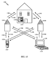
図15は、本開示の1つまたは複数の実施形態が有利に利用され得る例示的なワイヤレス通信システム1500を示す。説明のために、例示的なワイヤレス通信システム1500は、3つの遠隔ユニット1520、1530および1550、ならびに2つの基地局1540を示す。従来のワイヤレス通信システムは、はるかに多くのリモートユニットおよび基地局を有する場合があることを認識されよう。リモートユニット1520、1530、および1550は、半導体デバイス1525、1535、および1555を含んでよく、半導体デバイス1525、1535、および1555の1つまたは複数は、様々な例示的な実施形態による1つまたは複数の短縮マルチタップ補間フィルタ、たとえば、限定されることなく、図3から図10を参照して説明されたようなサブピクセル補間を実行するように構成可能であり、一態様では、図12および図13を参照して説明されたような双線形補間を実行するように、図11を参照して説明されたように構成可能である、図2を参照して説明された短縮サイクルマルチタップ補間フィルタを含み得る。図15は、基地局1540からリモートユニット1520、1530、および1550への順方向リンク信号1580、ならびにリモートユニット1520、1530、および1550から基地局1540への逆方向リンク信号1590を示す。
FIG. 15 illustrates an example
図15を参照すると、リモートユニット1520は携帯電話として示され、リモートユニット1530はポータブルコンピュータとして示され、リモートユニット1550はワイヤレスローカルループシステム内の固定位置リモートユニットとして示される。これらは、リモートユニット1520、1530、および1550のいずれかを実装し得るデバイスの例にすぎないことを理解されたい。たとえば、リモートユニット1520、1530、および1550は、携帯電話、ハンドヘルドパーソナル通信システム(PCS)ユニット、携帯情報端末などのポータブルデータユニット、(GPS対応デバイスなどの)ナビゲーションデバイス、セットトップボックス、音楽プレーヤ、ビデオプレーヤ、エンターテインメントユニット、メータ読取り機器などの固定位置データユニット、またはデータもしくはコンピュータ命令の記憶もしくは取出しを行う任意の他のデバイス、またはそれらの任意の組合せのうちの、1つまたは複数であり得る。図15は、本開示の教示による遠隔ユニットを示すが、本開示はこれらの例示的な示されたユニットに限定されない。本開示の実施形態は、試験および特性評価のための、メモリおよびオンチップ回路を含む能動的な集積回路を有する少なくとも1つの半導体ダイを含む、任意のデバイスにおいて適切に採用され得る。
Referring to FIG. 15,
情報および信号は、多種多様な技術および技法のいずれかを使用して表され得ることを当業者は諒解されよう。たとえば、上記の説明全体にわたって言及され得るデータ、命令、コマンド、情報、信号、ビット、シンボル、およびチップは、電圧、電流、電磁波、磁界または磁性粒子、光場または光学粒子、あるいはそれらの任意の組合せによって表され得る。 Those skilled in the art will appreciate that information and signals may be represented using any of a variety of different technologies and techniques. For example, data, instructions, commands, information, signals, bits, symbols, and chips that may be referred to throughout the above description are voltages, currents, electromagnetic waves, magnetic fields or magnetic particles, light fields or optical particles, or any of them Can be represented by a combination.
さらに、本明細書で開示された実施形態に関連して説明された様々な例示的な論理ブロック、モジュール、回路、およびアルゴリズムステップは、電子ハードウェア、コンピュータソフトウェア、または両方の組合せとして実装され得ることを、当業者は諒解されよう。ハードウェアとソフトウェアのこの互換性を明確に示すために、様々な例示的なコンポーネント、ブロック、モジュール、回路、およびステップは、上では概してそれらの機能に関して説明された。そのような機能がハードウェアとして実装されるか、ソフトウェアとして実装されるかは、具体的な適用例および全体的なシステムに課される設計制約に依存する。当業者は、説明された機能を具体的な適用例ごとに様々な方法で実装し得るが、そのような実装の決定は、本発明の範囲からの逸脱を生じるものと解釈されるべきではない。 Moreover, various exemplary logic blocks, modules, circuits, and algorithm steps described in connection with the embodiments disclosed herein may be implemented as electronic hardware, computer software, or a combination of both. Those skilled in the art will appreciate that. To clearly illustrate this interchangeability of hardware and software, various illustrative components, blocks, modules, circuits, and steps have been described above generally in terms of their functionality. Whether such functionality is implemented as hardware or software depends on the specific application and design constraints imposed on the overall system. Those skilled in the art may implement the described functionality in various ways for each specific application, but such implementation decisions should not be construed as departing from the scope of the present invention. .
本明細書で開示された実施形態と関連して説明された方法、シーケンス、および/またはアルゴリズムは、ハードウェアで、プロセッサによって実行されるソフトウェアモジュールで、またはその2つの組合せで直接具現化され得る。ソフトウェアモジュールは、RAMメモリ、フラッシュメモリ、ROMメモリ、EPROMメモリ、EEPROMメモリ、レジスタ、ハードディスク、リムーバブルディスク、CD-ROM、または当技術分野で知られている任意の他の形態の記憶媒体中に存在し得る。例示的な記憶媒体は、プロセッサが記憶媒体から情報を読み取り、記憶媒体に情報を書き込むことができるように、プロセッサに結合される。代替として、記憶媒体はプロセッサと一体であり得る。 The methods, sequences, and / or algorithms described in connection with the embodiments disclosed herein may be directly embodied in hardware, software modules executed by a processor, or a combination of the two. . Software modules reside in RAM memory, flash memory, ROM memory, EPROM memory, EEPROM memory, registers, hard disk, removable disk, CD-ROM, or any other form of storage medium known in the art Can do. An exemplary storage medium is coupled to the processor such that the processor can read information from, and write information to, the storage medium. In the alternative, the storage medium may be integral to the processor.
したがって、本発明の一実施形態は、説明された実施形態の方法に従うものとして、受信されたシリアルビットストリームを位相サンプリングするための方法を具現化する、コンピュータ可読媒体を含み得る。したがって、本発明は図示の例に限定されず、本明細書で説明された機能を実行するためのいかなる手段も、本発明の実施形態中に含まれる。 Accordingly, an embodiment of the present invention may include a computer-readable medium embodying a method for phase sampling a received serial bitstream as following the method of the described embodiment. Accordingly, the present invention is not limited to the illustrated examples, and any means for performing the functions described herein are included in embodiments of the present invention.
上記の開示は本発明の例示的な実施形態を示すが、添付の特許請求の範囲によって規定される本発明の範囲から逸脱することなく、本明細書において様々な変更および修正が行われ得ることに留意されたい。本明細書で説明された本発明の実施形態による方法クレームの機能、ステップおよび/または動作は、特定の順序で実行されなくてもよい。さらに、本発明の要素は、単数形で説明または特許請求されていることがあるが、単数形に限定することが明示的に述べられていない限り、複数形が企図される。 While the above disclosure represents exemplary embodiments of the present invention, various changes and modifications may be made herein without departing from the scope of the invention as defined by the appended claims. Please note that. The functions, steps and / or actions of a method claim according to embodiments of the invention described herein may not be performed in a particular order. Further, although elements of the invention may be described or claimed in the singular, the plural is contemplated unless expressly stated to be limited to the singular.
200 マルチタップ統合補間フィルタ
202 ピクセルウィンドウレジスタ
204 乗算器
206 タップ係数セットレジスタ
208 加算デバイス
210 累算器
212 2Sビットの符号付き飽和論理
300 ステップ移行のグラフィカルなモデル
302 ピクセルウィンドウ
402 状態
406 状態
410 内容
502 状態
572 領域
602 状態
606 状態
610 内容
672 領域
702 状態
772 領域
802 状態
806 状態
872 領域
902 状態
972 領域
1100 入力
1102_0 ピクセル行セクション
1102_2 ピクセル行セクション
1200 インターリーブされたクロマ成分の構成
1300 ピクセルのアレイ
1400 ピクセルのアレイ
1500 ワイヤレス通信システム
1520 リモートユニット
1525 半導体デバイス
1530 リモートユニット
1535 半導体デバイス
1540 基地局
1550 リモートユニット
1555 半導体デバイス
1580 順方向リンク信号
1590 逆方向リンク信号
200 Multi-tap integrated interpolation filter
202 pixel window register
204 multiplier
206 Tap coefficient set register
208 Addition device
210 Accumulator
212 2S-bit signed saturation logic
Graphical model of 300-step transition
302 pixel window
402 state
406 state
410 Contents
502 status
572 area
602 state
606 state
610 Contents
672 areas
702 state
772 areas
802 state
806 state
872 area
902 state
972 area
1100 input
1102_0 pixel row section
1102_2 pixel row section
1200 Composition of interleaved chroma components
1300 pixel array
1400 pixel array
1500 wireless communication system
1520 remote unit
1525 Semiconductor devices
1530 remote unit
1535 Semiconductor devices
1540 base station
1550 remote unit
1555 Semiconductor devices
1580 Forward link signal
1590 Reverse link signal
Claims (23)
前記ピクセルアレイからのピクセルのウィンドウレジスタと、所与のタップ係数セットを有するタップ係数レジスタとに基づいて、偶数番目の補間されたサブピクセルのセットを形成するステップと、
別の前記ピクセルによって前記ウィンドウレジスタを更新するステップと、
前記ウィンドウレジスタと前記タップ係数レジスタとに基づいて、奇数番目の補間されたサブピクセルのセットを形成するステップと、
所与の終了条件が満たされるまで、前記偶数番目の補間されたサブピクセルおよび前記奇数番目の補間されたサブピクセルを累算するステップであって、各累算するステップが、
別のタップ係数セットに基づいて前記タップ係数レジスタを更新し、別の前記ピクセルによって前記ウィンドウレジスタを更新するステップと、
前記ウィンドウレジスタと前記タップ係数レジスタとに基づいて、前記偶数番目の補間されたサブピクセルをインクリメントするステップと、
別の前記ピクセルによって前記ウィンドウレジスタを再び更新するステップと、
前記ウィンドウレジスタと前記タップ係数レジスタとに基づいて、前記奇数番目の補間されたサブピクセルをインクリメントするステップと
を含む、累算するステップと、
前記終了条件が満たされると、偶数番目の補間されたサブピクセルの前記セットおよび奇数番目の補間されたサブピクセルの前記セットを出力するステップとを含む、方法。 A method for generating interpolated pixels for a pixel array comprising:
Forming an even-numbered set of interpolated sub-pixels based on a window register of pixels from the pixel array and a tap coefficient register having a given set of tap coefficients;
Updating the window register with another of the pixels;
Forming an odd set of interpolated sub-pixels based on the window register and the tap coefficient register;
Accumulating the even-numbered interpolated sub-pixels and the odd-numbered interpolated sub-pixels until a given termination condition is satisfied, each accumulating step comprising:
Updating the tap coefficient register based on another set of tap coefficients and updating the window register with another of the pixels;
Incrementing the even-numbered interpolated subpixel based on the window register and the tap coefficient register;
Updating the window register again with another said pixel;
Incrementing the odd-numbered interpolated subpixels based on the window register and the tap coefficient register; and
Outputting the set of even-numbered interpolated subpixels and the set of odd-numbered interpolated subpixels when the termination condition is satisfied.
前記奇数番目の補間されたサブピクセルをインクリメントする各ステップが、別の対応する2個の積の合計によって、前記4個の奇数番目の補間されたサブピクセルの各々をインクリメントするステップを含む、請求項4に記載の方法。 Each step of incrementing the even-numbered interpolated subpixels includes incrementing each of the four even-numbered interpolated subpixels by the sum of another two corresponding products;
Wherein each step of incrementing said odd-numbered interpolated subpixel comprises incrementing each of said four odd-numbered interpolated subpixels by a sum of another corresponding two products. Item 5. The method according to Item 4.
前記奇数番目の補間されたサブピクセルを形成するステップが、少なくとも4個の奇数番目の補間されたサブピクセルを形成し、前記4個の奇数番目の補間されたサブピクセルの各々が、対応する2個の積の合計を有し、
前記偶数番目の補間されたサブピクセルをインクリメントする各ステップが、別の対応する2個の積の合計によって、前記4個の偶数番目の補間されたサブピクセルの各々をインクリメントするステップを含み、
前記奇数番目の補間されたサブピクセルをインクリメントする各ステップが、別の対応する2個の積の合計によって、前記4個の奇数番目の補間されたサブピクセルの各々をインクリメントするステップを含む、請求項1に記載の方法。 Forming the even-numbered interpolated sub-pixels forms at least four even-numbered interpolated sub-pixels, each of the four even-numbered interpolated sub-pixels being two products; Have a total of
Forming the odd-numbered interpolated sub-pixels forms at least four odd-numbered interpolated sub-pixels, each of the four odd-numbered interpolated sub-pixels corresponding to 2 Has a sum of products,
Each step of incrementing the even-numbered interpolated subpixels includes incrementing each of the four even-numbered interpolated subpixels by the sum of another two corresponding products;
Wherein each step of incrementing said odd-numbered interpolated subpixel comprises incrementing each of said four odd-numbered interpolated subpixels by a sum of another corresponding two products. Item 2. The method according to Item 1.
前記奇数番目の補間されたサブピクセルを形成するステップが、前記更新されたウィンドウからのピクセルを、前記タップ係数セットからの対応するタップ係数と乗算して、対応する積の合計を生成するステップと、積の前記合計のペアを合計して積の合計のセットを生成するステップと、積の合計の前記セットを、奇数番目の補間されたサブピクセルの前記セットとして前記累算器へとロードするステップと、奇数番目の補間されたサブピクセルの前記セットを、前記累算器レジスタから前記メモリへとオフロードするステップとを含む、請求項1に記載の方法。 Forming the even-numbered interpolated sub-pixels by multiplying pixels from a window with corresponding tap coefficients from the tap coefficient set to generate a sum of corresponding products; Summing pairs of sums to generate a set of sums of products; loading the set of sums of products into the accumulator as the set of even-numbered interpolated subpixels; and even-numbered Offloading said set of interpolated subpixels from an accumulator register to memory;
Forming the odd-numbered interpolated sub-pixels by multiplying pixels from the updated window with corresponding tap coefficients from the tap coefficient set to generate a sum of corresponding products; Summing the sum pairs of products to produce a set of sums of products, and loading the set of sums of products into the accumulator as the set of odd interpolated subpixels. The method of claim 1, comprising: offloading the set of odd-numbered interpolated subpixels from the accumulator register to the memory.
前記奇数番目の補間されたサブピクセルをインクリメントする各ステップが、奇数番目の補間されたサブピクセルの前記セットを前記メモリから前記累算器レジスタへとロードするステップと、別の更新されたウィンドウからのピクセルを、前記タップ係数セットからの対応するタップ係数と乗算して、対応する積の合計を生成するステップと、積の前記合計のペアを前記累算器レジスタからの対応する奇数番目の補間されたサブピクセルと合計して、累算された積の合計のセットを生成するステップと、累算された積の合計の前記セットを、奇数番目の補間されたサブピクセルの更新されたセットとして前記累算器レジスタへとロードするステップと、奇数番目の補間されたサブピクセルの前記セットを、前記累算器レジスタから前記メモリへとオフロードするステップとを含む、請求項9に記載の方法。 Each step of incrementing the even-numbered interpolated sub-pixels loads the set of even-numbered interpolated sub-pixels from the memory into the accumulator register; and from the updated window Multiplying a pixel by a corresponding tap coefficient from the updated tap coefficient set to generate a corresponding product sum; and converting the sum pair of products to a corresponding even number from the accumulator register Generating a set of accumulated products summed with the interpolated sub-pixels of the updated sub-pixels, and updating the set of accumulated product sums of the even-numbered interpolated sub-pixels. Loading the set of accumulator registers as a set and the set of even-numbered interpolated subpixels to the accumulator register And a step of off-loaded into the memory,
Each step of incrementing the odd-numbered interpolated subpixels loads the set of odd-numbered interpolated subpixels from the memory into the accumulator register, and from another updated window Are multiplied by corresponding tap coefficients from the tap coefficient set to generate corresponding product sums, and the sum pairs of products are corresponding odd-numbered interpolations from the accumulator registers. Generating a set of accumulated product sums, and summing the set of accumulated products as an updated set of odd interpolated subpixels. Loading into the accumulator register and the set of odd interpolated sub-pixels from the accumulator register to the memory; To to include the steps of offloading method of claim 9.
前記ピクセルアレイからのピクセルのウィンドウと、所与のタップ係数セットとに基づいて、偶数番目の補間されたサブピクセルのセットを形成するための手段と、
別の前記ピクセルによって前記ウィンドウを更新するための手段と、
ピクセルの前記ウィンドウと、前記所与のタップ係数セットとに基づいて、奇数番目の補間されたサブピクセルのセットを形成するための手段と、
所与の終了条件が満たされるまで、前記偶数番目の補間されたサブピクセルおよび前記奇数番目の補間されたサブピクセルを累算するための手段であって、
前記タップ係数セットを更新して別の前記ピクセルによって前記ウィンドウを更新し、
ピクセルの前記ウィンドウと前記タップ係数セットとに基づいて、前記偶数番目の補間されたサブピクセルをインクリメントし、
別の前記ピクセルによってピクセルの前記ウィンドウを更新し、
ピクセルの前記ウィンドウと前記タップ係数セットとに基づいて、前記奇数番目の補間されたサブピクセルをインクリメントする
ように構成される、手段と、
前記所与の終了条件が満たされると、前記偶数番目の補間されたサブピクセルおよび前記奇数番目の補間されたサブピクセルを出力するための手段とを含む、装置。 An apparatus for generating interpolated pixels for a pixel array comprising:
Means for forming an even-numbered set of interpolated subpixels based on a window of pixels from the pixel array and a given set of tap coefficients;
Means for updating the window with another said pixel;
Means for forming an odd set of interpolated sub-pixels based on the window of pixels and the given set of tap coefficients;
Means for accumulating the even-numbered interpolated sub-pixels and the odd-numbered interpolated sub-pixels until a given termination condition is satisfied, comprising:
Update the window with another pixel by updating the tap coefficient set;
Incrementing the even-numbered interpolated subpixel based on the window of pixels and the tap coefficient set;
Update the window of pixels with another said pixel;
Means configured to increment the odd-numbered interpolated subpixels based on the window of pixels and the tap coefficient set;
Means for outputting the even-numbered interpolated sub-pixels and the odd-numbered interpolated sub-pixels when the given termination condition is met.
奇数番目の補間されたサブピクセルの前記セットを形成するための前記手段が、4個の奇数番目の補間されたサブピクセルを含むように前記セットを形成するように構成され、前記4個の奇数番目の補間されたサブピクセルの各々が、対応する2個の積の合計を有する、請求項13に記載の、ピクセルアレイに対する補間されたピクセルを生成するための装置。 The means for forming the set of even-numbered interpolated subpixels is configured to form the set to include four even-numbered interpolated subpixels; Each of the th interpolated subpixels has a sum of two products;
The means for forming the set of odd-numbered interpolated subpixels is configured to form the set to include four odd-numbered interpolated subpixels; 14. The apparatus for generating interpolated pixels for a pixel array according to claim 13, wherein each of the th interpolated subpixels has a corresponding sum of two products.
前記ピクセルアレイからのピクセルのウィンドウと、所与のタップ係数セットとに基づいて、偶数番目の補間されたサブピクセルのセットを形成させ、
別の前記ピクセルによって前記ウィンドウを更新させ、
ピクセルの前記ウィンドウと、前記所与のタップ係数セットとに基づいて、奇数番目の補間されたサブピクセルのセットを形成させ、
所与の終了条件が満たされるまで、偶数番目の補間されたサブピクセルおよび奇数番目の補間されたサブピクセルの前記セットを累算させる命令を含み、前記命令が、前記プロセッサ装置に、
前記タップ係数セットを更新して別の前記ピクセルによってピクセルの前記ウィンドウを更新し、
ピクセルの前記ウィンドウおよび前記タップ係数セットに基づいて、前記偶数番目の補間されたサブピクセルをインクリメントし、
別の前記ピクセルによってピクセルの前記ウィンドウを再び更新し、
ピクセルの前記ウィンドウと前記タップ係数セットとに基づいて、前記奇数番目の補間されたサブピクセルをインクリメントする
ことによって累算させ、
前記偶数番目の補間されたサブピクセルおよび前記奇数番目の補間されたサブピクセルを出力させる、コンピュータ可読記録媒体。 A computer readable recording medium comprising instructions that, when executed by a processor device in a wireless communication system, cause the processor device to perform operations to implement a method for generating interpolated pixels for a pixel array, comprising: In the processor unit,
Forming an even set of interpolated subpixels based on a window of pixels from the pixel array and a given set of tap coefficients;
Updating the window with another pixel;
Forming an odd set of interpolated sub-pixels based on the window of pixels and the given set of tap coefficients;
Including instructions for accumulating the set of even-numbered interpolated sub-pixels and odd-numbered interpolated sub-pixels until a given termination condition is satisfied, the instructions comprising:
Updating the tap coefficient set to update the window of pixels with another pixel;
Incrementing the even-numbered interpolated subpixel based on the window of pixels and the tap coefficient set;
Update the window of pixels again with another said pixel,
Accumulating by incrementing the odd interpolated sub-pixel based on the window of pixels and the tap coefficient set;
A computer-readable recording medium for outputting the even-numbered interpolated subpixels and the odd-numbered interpolated subpixels.
前記プロセッサ装置に、前記奇数番目の補間されたサブピクセルをインクリメントさせる前記命令が、前記プロセッサ装置に、前記4個の奇数番目の補間されたサブピクセルの各々を、別の対応する2個の積の合計によってインクリメントさせ、
前記奇数番目の補間されたサブピクセルをインクリメントする各ステップが、別の対応する2個の積の合計によって、前記4個の奇数番目の補間されたサブピクセルの各々をインクリメントするステップを含む、請求項18に記載のコンピュータ可読記録媒体。 The instruction to increment the even-numbered interpolated subpixels to the processor unit causes the processor unit to replace each of the four even-numbered interpolated subpixels with another corresponding two products. Increment by the sum of
The instruction to cause the processor unit to increment the odd-numbered interpolated sub-pixels causes the processor unit to replace each of the four odd-numbered interpolated sub-pixels with another corresponding two products. Increment by the sum of
Wherein each step of incrementing said odd-numbered interpolated subpixel comprises incrementing each of said four odd-numbered interpolated subpixels by a sum of another corresponding two products. Item 19. A computer-readable recording medium according to Item 18.
前記ピクセルアレイからのピクセルのウィンドウと、所与のタップ係数セットとに基づいて、偶数番目の補間されたサブピクセルのセットを形成し、
別の前記ピクセルによって前記ウィンドウを更新し、
ピクセルの前記ウィンドウと、前記所与のタップ係数セットとに基づいて、奇数番目の補間されたサブピクセルのセットを形成し、
所与の終了条件が満たされるまで、前記偶数番目の補間されたサブピクセルおよび前記奇数番目の補間されたサブピクセルを累算するように構成され、前記論理回路が、
前記タップ係数セットを更新して前記別のピクセルによって前記ウィンドウを更新し、
ピクセルの前記ウィンドウおよび前記タップ係数セットに基づいて、前記偶数番目の補間されたサブピクセルをインクリメントし、
別の前記ピクセルによってピクセルの前記ウィンドウを更新し、
ピクセルの前記ウィンドウと前記タップ係数セットとに基づいて、前記奇数番目の補間されたサブピクセルをインクリメントする
ことによって累算し、
前記所与の終了条件が満たされると、前記偶数番目の補間されたサブピクセルおよび前記奇数番目の補間されたサブピクセルを出力するように構成される、装置。 An apparatus for generating interpolated pixels for a pixel array comprising a logic circuit having an input for receiving pixels from the pixel array, the logic circuit comprising:
Forming an even-numbered set of interpolated sub-pixels based on a window of pixels from the pixel array and a given set of tap coefficients;
Update the window with another said pixel;
Forming an odd set of interpolated sub-pixels based on the window of pixels and the given set of tap coefficients;
Configured to accumulate the even-numbered interpolated subpixels and the odd-numbered interpolated subpixels until a given termination condition is satisfied, the logic circuit comprising:
Update the tap coefficient set to update the window with the other pixels;
Incrementing the even-numbered interpolated subpixel based on the window of pixels and the tap coefficient set;
Update the window of pixels with another said pixel;
Accumulate by incrementing the odd interpolated sub-pixel based on the window of pixels and the tap coefficient set;
An apparatus configured to output the even-numbered interpolated subpixels and the odd-numbered interpolated subpixels when the given termination condition is met.
Applications Claiming Priority (3)
| Application Number | Priority Date | Filing Date | Title |
|---|---|---|---|
| US13/450,734 | 2012-04-19 | ||
| US13/450,734 US8855446B2 (en) | 2012-04-19 | 2012-04-19 | Accelerated video compression multi-tap filter and bilinear interpolator |
| PCT/US2013/037206 WO2013158903A1 (en) | 2012-04-19 | 2013-04-18 | Accelerated multi-tap filter and bilinear interpolator for video compression |
Publications (3)
| Publication Number | Publication Date |
|---|---|
| JP2015515225A true JP2015515225A (en) | 2015-05-21 |
| JP2015515225A5 JP2015515225A5 (en) | 2016-06-02 |
| JP6382795B2 JP6382795B2 (en) | 2018-08-29 |
Family
ID=48325888
Family Applications (1)
| Application Number | Title | Priority Date | Filing Date |
|---|---|---|---|
| JP2015507184A Expired - Fee Related JP6382795B2 (en) | 2012-04-19 | 2013-04-18 | Accelerated video compression multi-tap filter and bilinear interpolator |
Country Status (5)
| Country | Link |
|---|---|
| US (1) | US8855446B2 (en) |
| EP (1) | EP2839650A1 (en) |
| JP (1) | JP6382795B2 (en) |
| CN (1) | CN104247435B (en) |
| WO (1) | WO2013158903A1 (en) |
Families Citing this family (2)
| Publication number | Priority date | Publication date | Assignee | Title |
|---|---|---|---|---|
| US11409525B2 (en) * | 2018-01-24 | 2022-08-09 | Intel Corporation | Apparatus and method for vector multiply and accumulate of packed words |
| CN108322759B (en) * | 2018-02-24 | 2021-02-05 | 北京奇艺世纪科技有限公司 | Pixel value acquisition method and device and electronic equipment |
Citations (2)
| Publication number | Priority date | Publication date | Assignee | Title |
|---|---|---|---|---|
| JPH10124656A (en) * | 1996-10-18 | 1998-05-15 | Sony Corp | Image processing apparatus and method |
| EP1605704A2 (en) * | 2004-05-28 | 2005-12-14 | Samsung Electronics Co., Ltd. | Image interpolation apparatus and methods |
Family Cites Families (10)
| Publication number | Priority date | Publication date | Assignee | Title |
|---|---|---|---|---|
| US5500811A (en) | 1995-01-23 | 1996-03-19 | Microunity Systems Engineering, Inc. | Finite impulse response filter |
| US6470370B2 (en) | 1995-09-05 | 2002-10-22 | Intel Corporation | Method and apparatus for multiplying and accumulating complex numbers in a digital filter |
| US6188803B1 (en) | 1996-10-18 | 2001-02-13 | Sony Corporation | Image processing device |
| US6061521A (en) | 1996-12-02 | 2000-05-09 | Compaq Computer Corp. | Computer having multimedia operations executable as two distinct sets of operations within a single instruction cycle |
| US6175592B1 (en) | 1997-03-12 | 2001-01-16 | Matsushita Electric Industrial Co., Ltd. | Frequency domain filtering for down conversion of a DCT encoded picture |
| US8463837B2 (en) | 2001-10-29 | 2013-06-11 | Intel Corporation | Method and apparatus for efficient bi-linear interpolation and motion compensation |
| KR100624429B1 (en) * | 2003-07-16 | 2006-09-19 | 삼성전자주식회사 | A video encoding/ decoding apparatus and method for color image |
| CN100455025C (en) * | 2005-07-21 | 2009-01-21 | 华为技术有限公司 | A Fractional Pixel Interpolation Method and Codec Device |
| CN101009842B (en) * | 2006-01-11 | 2012-02-01 | 华为技术有限公司 | Method and device for value insertion in the hierarchical video compression |
| CN101938644A (en) * | 2009-07-03 | 2011-01-05 | 哈尔滨工业大学深圳研究生院 | Video Compression 1/2 Pixel Accuracy Motion Estimation Hardware Implementation Method |
-
2012
- 2012-04-19 US US13/450,734 patent/US8855446B2/en not_active Expired - Fee Related
-
2013
- 2013-04-18 JP JP2015507184A patent/JP6382795B2/en not_active Expired - Fee Related
- 2013-04-18 EP EP13721171.0A patent/EP2839650A1/en not_active Withdrawn
- 2013-04-18 CN CN201380020605.0A patent/CN104247435B/en not_active Expired - Fee Related
- 2013-04-18 WO PCT/US2013/037206 patent/WO2013158903A1/en not_active Ceased
Patent Citations (2)
| Publication number | Priority date | Publication date | Assignee | Title |
|---|---|---|---|---|
| JPH10124656A (en) * | 1996-10-18 | 1998-05-15 | Sony Corp | Image processing apparatus and method |
| EP1605704A2 (en) * | 2004-05-28 | 2005-12-14 | Samsung Electronics Co., Ltd. | Image interpolation apparatus and methods |
Non-Patent Citations (1)
| Title |
|---|
| JUYUP LEE(外2名): "H.264 DECODER OPTIMIZATION EXPLOITING SIMD INSTRUCTIONS", CIRCUITS AND SYSTEMS, 2004. PROCEEDINGS. THE 2004 IEEE ASIA-PACIFIC CONFERENCE ON, JPN6017015061, 6 December 2004 (2004-12-06), US, pages 1149 - 1152, XP010783438, DOI: doi:10.1109/APCCAS.2004.1413088 * |
Also Published As
| Publication number | Publication date |
|---|---|
| JP6382795B2 (en) | 2018-08-29 |
| US20130279827A1 (en) | 2013-10-24 |
| WO2013158903A1 (en) | 2013-10-24 |
| CN104247435B (en) | 2018-03-30 |
| US8855446B2 (en) | 2014-10-07 |
| EP2839650A1 (en) | 2015-02-25 |
| CN104247435A (en) | 2014-12-24 |
Similar Documents
| Publication | Publication Date | Title |
|---|---|---|
| EP1120747A2 (en) | Motion estimator | |
| KR101578052B1 (en) | Motion estimation device and Moving image encoding device having the same | |
| US8698906B2 (en) | Image processing device, imaging device, information storage medium, and image processing method | |
| US9210341B2 (en) | Image processing device, imaging device, information storage medium, and image processing method | |
| JP4837615B2 (en) | Image processing method and image processing apparatus | |
| US20090016634A1 (en) | Half pixel interpolator for video motion estimation accelerator | |
| US8594443B2 (en) | Method and apparatus for motion compensation supporting multicodec | |
| JP6382795B2 (en) | Accelerated video compression multi-tap filter and bilinear interpolator | |
| KR101170632B1 (en) | Repetitive object detecting device and method | |
| JP4824703B2 (en) | Two-dimensional filter arithmetic apparatus and method | |
| EP1605704A2 (en) | Image interpolation apparatus and methods | |
| Wu et al. | Efficient hierarchical motion estimation algorithm and its VLSI architecture | |
| JP2007096431A (en) | Digital video format down-conversion apparatus and method with arbitrary conversion ratio | |
| Celebi et al. | An all binary sub-pixel motion estimation approach and its hardware architecture | |
| JP2009239698A (en) | Video image converting device, and video image converting method | |
| US10397579B2 (en) | Sampling rate converter | |
| Jung et al. | A 4-way pipelined processing architecture for three-step search block-matching motion estimation | |
| KR101059649B1 (en) | Encoding device, method and decoding device using adaptive interpolation filter | |
| JP2009290710A (en) | Image processing apparatus and display unit | |
| JP2002509627A (en) | Method and apparatus for generating half-pixel SAD | |
| EP1056295A1 (en) | Filter arithmetic device | |
| KR101428531B1 (en) | A Multi-Frame-Based Super Resolution Method by Using Motion Vector Normalization and Edge Pattern Analysis | |
| Tasdizen et al. | A high performance reconfigurable motion estimation hardware architecture | |
| US6560286B1 (en) | Field frame motion design for digital video decoder | |
| JP4972321B2 (en) | Method and apparatus for scanning pixels in a sequence of images representing temporal recurrence and method and apparatus for estimating current frame motion with respect to a reference frame |
Legal Events
| Date | Code | Title | Description |
|---|---|---|---|
| A529 | Written submission of copy of amendment under article 34 pct |
Free format text: JAPANESE INTERMEDIATE CODE: A529 Effective date: 20141020 |
|
| A521 | Request for written amendment filed |
Free format text: JAPANESE INTERMEDIATE CODE: A523 Effective date: 20160404 |
|
| A621 | Written request for application examination |
Free format text: JAPANESE INTERMEDIATE CODE: A621 Effective date: 20160404 |
|
| A977 | Report on retrieval |
Free format text: JAPANESE INTERMEDIATE CODE: A971007 Effective date: 20170324 |
|
| A131 | Notification of reasons for refusal |
Free format text: JAPANESE INTERMEDIATE CODE: A131 Effective date: 20170508 |
|
| A521 | Request for written amendment filed |
Free format text: JAPANESE INTERMEDIATE CODE: A523 Effective date: 20170621 |
|
| A131 | Notification of reasons for refusal |
Free format text: JAPANESE INTERMEDIATE CODE: A131 Effective date: 20171211 |
|
| A521 | Request for written amendment filed |
Free format text: JAPANESE INTERMEDIATE CODE: A523 Effective date: 20180307 |
|
| TRDD | Decision of grant or rejection written | ||
| A01 | Written decision to grant a patent or to grant a registration (utility model) |
Free format text: JAPANESE INTERMEDIATE CODE: A01 Effective date: 20180709 |
|
| A61 | First payment of annual fees (during grant procedure) |
Free format text: JAPANESE INTERMEDIATE CODE: A61 Effective date: 20180802 |
|
| R150 | Certificate of patent or registration of utility model |
Ref document number: 6382795 Country of ref document: JP Free format text: JAPANESE INTERMEDIATE CODE: R150 |
|
| R250 | Receipt of annual fees |
Free format text: JAPANESE INTERMEDIATE CODE: R250 |
|
| R250 | Receipt of annual fees |
Free format text: JAPANESE INTERMEDIATE CODE: R250 |
|
| LAPS | Cancellation because of no payment of annual fees |