JP2015222912A - Linearizer - Google Patents
Linearizer Download PDFInfo
- Publication number
- JP2015222912A JP2015222912A JP2014107276A JP2014107276A JP2015222912A JP 2015222912 A JP2015222912 A JP 2015222912A JP 2014107276 A JP2014107276 A JP 2014107276A JP 2014107276 A JP2014107276 A JP 2014107276A JP 2015222912 A JP2015222912 A JP 2015222912A
- Authority
- JP
- Japan
- Prior art keywords
- linearizer
- diode
- terminal
- connection point
- voltage
- Prior art date
- Legal status (The legal status is an assumption and is not a legal conclusion. Google has not performed a legal analysis and makes no representation as to the accuracy of the status listed.)
- Pending
Links
Images


Classifications
-
- H—ELECTRICITY
- H03—ELECTRONIC CIRCUITRY
- H03F—AMPLIFIERS
- H03F1/00—Details of amplifiers with only discharge tubes, only semiconductor devices or only unspecified devices as amplifying elements
- H03F1/32—Modifications of amplifiers to reduce non-linear distortion
- H03F1/3241—Modifications of amplifiers to reduce non-linear distortion using predistortion circuits
- H03F1/3276—Modifications of amplifiers to reduce non-linear distortion using predistortion circuits using the nonlinearity inherent to components, e.g. a diode
-
- H—ELECTRICITY
- H03—ELECTRONIC CIRCUITRY
- H03F—AMPLIFIERS
- H03F3/00—Amplifiers with only discharge tubes or only semiconductor devices as amplifying elements
- H03F3/189—High frequency amplifiers, e.g. radio frequency amplifiers
- H03F3/19—High frequency amplifiers, e.g. radio frequency amplifiers with semiconductor devices only
-
- H—ELECTRICITY
- H03—ELECTRONIC CIRCUITRY
- H03F—AMPLIFIERS
- H03F2200/00—Indexing scheme relating to amplifiers
- H03F2200/387—A circuit being added at the output of an amplifier to adapt the output impedance of the amplifier
-
- H—ELECTRICITY
- H03—ELECTRONIC CIRCUITRY
- H03F—AMPLIFIERS
- H03F2201/00—Indexing scheme relating to details of amplifiers with only discharge tubes, only semiconductor devices or only unspecified devices as amplifying elements covered by H03F1/00
- H03F2201/32—Indexing scheme relating to modifications of amplifiers to reduce non-linear distortion
- H03F2201/3215—To increase the output power or efficiency
Abstract
Description
本発明は、高周波増幅器の歪特性を改善するダイオードリニアライザに関する。 The present invention relates to a diode linearizer that improves the distortion characteristics of a high-frequency amplifier.
近年、窒化物半導体(例えばGaN)を用いたトランジスタの研究開発が盛んであり、その応用例として通信用高出力増幅器がある。GaNを用いた増幅器は、従来の化合物半導体(例えばGaAs)を用いた増幅器と比較し、高出力化できる。しかし、低い入力電力から利得が緩やかに減少するGaN特有のソフトコンプレッションにより、特にAMAM特性が低下するという問題がある。 In recent years, research and development of transistors using nitride semiconductors (for example, GaN) has been active, and an application example thereof is a high-power amplifier for communication. An amplifier using GaN can achieve higher output than an amplifier using a conventional compound semiconductor (for example, GaAs). However, there is a problem that the AMAM characteristic is particularly deteriorated due to the soft compression peculiar to GaN in which the gain gradually decreases from a low input power.
AMAM特性を補償するアナログプレディストーションとして、ダイオードを用いたリニアライザがある。その中でも並列ダイオードリニアライザは回路構成が簡易であり、小型かつ低消費電力である(例えば、非特許文献1,2参照)。
As an analog predistortion that compensates for AMAM characteristics, there is a linearizer using a diode. Among them, the parallel diode linearizer has a simple circuit configuration, a small size, and low power consumption (see, for example, Non-Patent
SiC基板を用いたGaN系の増幅器MMICにリニアライザを内蔵する場合、エピ基板が高価なため、極力小型な回路が望まれている。並列ダイオードリニアライザは簡易な構成で済むためGaN−MMICにとっては最適な回路である。 When a linearizer is built in a GaN-based amplifier MMIC using a SiC substrate, an epi substrate is expensive, and thus a circuit as small as possible is desired. Since the parallel diode linearizer has a simple configuration, it is an optimal circuit for the GaN-MMIC.
並列ダイオードリニアライザは、通常、その前段又は後段に接続される増幅器のAMAM,AMPMの逆特性を有するように設計される。リニアライザのダイオードに印加される電圧によってリニアライザのAMAM,AMPM特性が変化する。このため、リニアライザはAMAM,AMPMを制御する制御端子を有しており、増幅器のAMAM,AMPMに応じてリニアライザの印加電圧を制御・調整している。 The parallel diode linearizer is usually designed to have the inverse characteristics of AMAM and AMPM of the amplifier connected to the preceding stage or the subsequent stage. The AMAM and AMPM characteristics of the linearizer change depending on the voltage applied to the diode of the linearizer. For this reason, the linearizer has a control terminal for controlling AMAM and AMPM, and controls and adjusts the voltage applied to the linearizer according to the AMAM and AMPM of the amplifier.
リニアライザにバイアス印加すると、ダイオードのアノード電極に電流が流れる。このため、アノード電極メタルにマイグレーションが発生して信頼性が低下する。これを防ぐためにはアノード電流値を制限する必要があり、リニアライザ設計の自由度が抑制される。 When a bias is applied to the linearizer, a current flows through the anode electrode of the diode. For this reason, migration occurs in the anode electrode metal and the reliability is lowered. In order to prevent this, it is necessary to limit the anode current value, and the degree of freedom in designing the linearizer is suppressed.
本発明は、上述のような課題を解決するためになされたもので、その目的は信頼性を改善して設計の自由度を向上させることができるリニアライザを得るものである。 The present invention has been made to solve the above-described problems, and an object of the present invention is to obtain a linearizer capable of improving reliability and improving design freedom.
本発明に係るリニアライザは、入力端子と、出力端子と、前記入力端子と前記出力端子との間に接続された接続点と、前記接続点と接地点との間に接続されたダイオードと、電圧端子と、前記電圧端子と前記接続点との間に接続された抵抗とを備え、前記電圧端子に0Vが印加されていることを特徴とする。 The linearizer according to the present invention includes an input terminal, an output terminal, a connection point connected between the input terminal and the output terminal, a diode connected between the connection point and the ground point, and a voltage. And a resistor connected between the voltage terminal and the connection point, and 0 V is applied to the voltage terminal.
本発明ではリニアライザの電圧端子に0Vを印加することにより、ダイオードのアノード電流が低くて済むため、アノード電極メタルにマイグレーションが発生せず、信頼性を向上させることができる。そして、アノード電流値を制限する必要が無いため、リニアライザ設計の自由度を向上させることができる。 In the present invention, by applying 0 V to the voltage terminal of the linearizer, the anode current of the diode can be reduced, so that no migration occurs in the anode electrode metal, and the reliability can be improved. And since it is not necessary to restrict | limit an anode electric current value, the freedom degree of a linearizer design can be improved.
本発明の実施の形態に係るリニアライザについて図面を参照して説明する。同じ又は対応する構成要素には同じ符号を付し、説明の繰り返しを省略する場合がある。 A linearizer according to an embodiment of the present invention will be described with reference to the drawings. The same or corresponding components are denoted by the same reference numerals, and repeated description may be omitted.
実施の形態1.
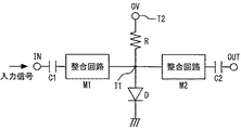
図1は、本発明の実施の形態1に係るリニアライザを示す回路図である。入力端子INからKu帯の高周波信号が入力される。入力端子INと出力端子OUTとの間に接続点T1が接続されている。入力端子INと接続点T1との間にキャパシタC1と整合回路M1が接続されている。接続点T1と出力端子OUTとの間にキャパシタC2と整合回路M2が接続されている。キャパシタC1,C2はDCカット用である。接続点T1と接地点との間にダイオードDが接続されている。電圧端子T2と接続点T1との間に抵抗Rが接続されている。抵抗Rの抵抗値は2000Ωである。電圧端子T2に0Vが印加されている。
FIG. 1 is a circuit diagram showing a linearizer according to
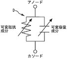
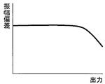
図2は、ダイオードの等価回路を示す図である。ダイオードDは可変抵抗成分と可変容量成分を有する。図3は、本発明の実施の形態1に係るリニアライザのAMAM特性を示す図である。図4は、本発明の実施の形態1に係るリニアライザのAMPM特性を示す図である。
FIG. 2 is a diagram showing an equivalent circuit of a diode. The diode D has a variable resistance component and a variable capacitance component. FIG. 3 is a diagram showing AMAM characteristics of the linearizer according to
入力信号の周波数がKu帯と高い場合、ダイオードDの容量成分のインピーダンス(1/ωC)が低くなる。このため、接続点T1の電位が0Vで抵抗成分のインピーダンスが高くてもダイオードDとしてはインピーダンスが低くなる。従って、小信号時はダイオードDのインピーダンスが低いため、リニアライザのロスは大きくなる。 When the frequency of the input signal is as high as the Ku band, the impedance (1 / ωC) of the capacitance component of the diode D is low. For this reason, even if the potential of the connection point T1 is 0V and the impedance of the resistance component is high, the impedance of the diode D is low. Therefore, when the signal is small, the impedance of the diode D is low, and the loss of the linearizer becomes large.
一方、大信号時はダイオードDに順方向に電流が流れ、接続点T1の電位は0Vから低電圧側にシフトするため、抵抗成分のインピーダンスは高くなる。低電圧側(本実施の形態では負電圧側)にシフトすると容量成分が低くなる。従って、ダイオードDのインピーダンスが高くなり、リニアライザのロスが小さくなる。これにより、図3に示すようにAMAMのダイナミックレンジを確保することができる。AMPM特性については非特許文献1,2と同じ動作原理である。
On the other hand, in the case of a large signal, a current flows through the diode D in the forward direction and the potential at the connection point T1 shifts from 0 V to the low voltage side, so that the impedance of the resistance component increases. When shifting to the low voltage side (in this embodiment, the negative voltage side), the capacitance component decreases. Therefore, the impedance of the diode D increases and the loss of the linearizer decreases. As a result, the AMAM dynamic range can be secured as shown in FIG. The AMPM characteristic is the same operation principle as in
本実施の形態では、リニアライザの電圧端子に0Vを印加することにより、ダイオードDのアノード電流が低くて済むため、アノード電極メタルにマイグレーションが発生せず、信頼性を向上させることができる。そして、アノード電流値を制限する必要が無いため、リニアライザ設計の自由度を向上させることができる。なお、本実施の形態ではダイオードDのカソードを接地したが、アノードを接地した場合でも、電流の向きが変わるだけであり、同様の効果が得られる。 In this embodiment, by applying 0 V to the voltage terminal of the linearizer, the anode current of the diode D can be reduced, so that migration does not occur in the anode electrode metal, and the reliability can be improved. And since it is not necessary to restrict | limit an anode electric current value, the freedom degree of a linearizer design can be improved. In the present embodiment, the cathode of the diode D is grounded, but even when the anode is grounded, only the direction of the current is changed, and the same effect can be obtained.
実施の形態2.
図5は、本発明の実施の形態2に係るリニアライザを示す回路図である。リニアライザの電圧端子T2が接地されている。ダイオードDはドレインとソースを短絡したHEMT構造を有する。その他の構成は実施の形態1と同様である。
FIG. 5 is a circuit diagram showing a linearizer according to
電圧端子T2を接地しているため、リニアライザ用の電源が不要となる。そして、MMIC内の配線レイアウトが簡単になる。従って、アンプモジュールの構成を簡略化及び小型化し、コストを削減することができる。 Since the voltage terminal T2 is grounded, a power supply for the linearizer becomes unnecessary. And the wiring layout in the MMIC is simplified. Therefore, the configuration of the amplifier module can be simplified and reduced in size, and the cost can be reduced.
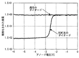
図6はダイオードの容量とアノード電圧の関係を示す図である。本実施の形態ではバイアス点である0Vから負電圧方向にシフトする。これに対して、通常のダイオードでは負電圧領域における容量変化量はほとんど無い。一方、HEMT系のダイオード(ゲートをアノード、短絡したドレインとソースをカソードとしたダイオード)では容量変化量は2桁もある。そこで、電圧に対する容量成分の変化量が大きいHEMT系のダイオードを使うことでリニアライザ特性のダイナミックレンジを大きくできる。また、HEMTプロセスのダイオードを用いれば、リニアライザと増幅器をMMIC上に集積できる。 FIG. 6 is a diagram showing the relationship between the capacitance of the diode and the anode voltage. In the present embodiment, the bias point shifts from 0 V in the negative voltage direction. In contrast, ordinary diodes have almost no capacitance change in the negative voltage region. On the other hand, the HEMT type diode (a diode having a gate as an anode, a short-circuited drain and a source as a cathode) has a capacitance change amount of two digits. Therefore, the dynamic range of the linearizer characteristic can be increased by using a HEMT diode having a large amount of change in capacitance component with respect to voltage. If a diode of HEMT process is used, a linearizer and an amplifier can be integrated on the MMIC.
実施の形態3.
図7は、本発明の実施の形態3に係るリニアライザを示す回路図である。ダイオードDのカソードと接地点との間にインダクタLが接続されている。その他の構成は実施の形態2と同様である。
FIG. 7 is a circuit diagram showing a linearizer according to
図8は、歪特性を補償される増幅器のAMAM,AMPM特性を示す図である。AMAMは単調に減少するが、AMPMは一旦増加した後、減少する。図9は、本発明の実施の形態3に係るリニアライザのAMPM,AMPM特性を示す図である。インダクタLを挿入することでリニアライザのAMPM特性を反転させることができる。従って、本実施の形態のリニアライザにより増幅器のAMPM特性を飽和領域(AMPMが反転した後の領域)まで補償することができる。 FIG. 8 is a diagram showing AMAM and AMPM characteristics of an amplifier whose distortion characteristics are compensated. AMAM decreases monotonously, but AMPM increases once and then decreases. FIG. 9 is a diagram showing AMPM and AMPM characteristics of the linearizer according to the third embodiment of the present invention. By inserting the inductor L, the AMPM characteristic of the linearizer can be inverted. Therefore, the AMPM characteristic of the amplifier can be compensated up to the saturation region (region after the AMPM is inverted) by the linearizer of the present embodiment.
実施の形態4.
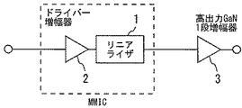
図10は、本発明の実施の形態4に係るリニアライザを示すブロック図である。実施の形態1〜3の何れかのリニアライザ1の前段に、GaN系のトランジスタ(例えばGaN−HEMT)を有するドライバー増幅器2が設けられている。リニアライザ1の後段に高出力GaN1段増幅器3が設けられている。ドライバー増幅器2がリニアライザ1の入力端子INに出力信号を供給する。ドライバー増幅器2の出力信号でリニアライザ1を励振することでリニアライザ動作させる。
FIG. 10 is a block diagram showing a linearizer according to
図8に示したようにGaN系の増幅器は高出力化を期待できるものの、GaN特有のソフトコンプレッションにより利得が緩やかに低下していく。これを補償するためリニアライザ1が必要であるが、後段が高出力のため、リニアライザ1の出力も高くしておく必要がある。このためには、ダイオードDをGaN系にすればよい。ただし、GaN系のダイオードの立ち上がり電圧は約1.0Vと、従来のGaAs系のダイオードの0.7Vと比較し0.3V高いため、リニアライザの利得立ち上がりに大きな入力電力が必要である。GaN−HEMTはGaAs−HEMTと比較し高電力密度を有しているため、ドライバー増幅器2をGaN系トランジスタにしておけば、リニアライザ1を十分にドライブすることができる。
As shown in FIG. 8, the GaN-based amplifier can be expected to have a high output, but the gain gradually decreases due to the soft compression specific to GaN. In order to compensate for this, the
また、ダイオードD専用のプロセスは不要でHEMTプロセスで実現可能なため、リニアライザ1とドライバー増幅器2をMMICとして集積化でき、回路面積を縮小することができる。
In addition, since a process dedicated to the diode D is unnecessary and can be realized by a HEMT process, the
1 リニアライザ、2 ドライバー増幅器、C1,C2 キャパシタ、D ダイオード、IN 入力端子、L インダクタ、OUT 出力端子、R 抵抗、T1 接続点、T2 電圧端子 1 linearizer, 2 driver amplifier, C1, C2 capacitor, D diode, IN input terminal, L inductor, OUT output terminal, R resistance, T1 connection point, T2 voltage terminal
Claims (6)
出力端子と、
前記入力端子と前記出力端子との間に接続された接続点と、
前記接続点と接地点との間に接続されたダイオードと、
電圧端子と、
前記電圧端子と前記接続点との間に接続された抵抗とを備え、
前記電圧端子に0Vが印加されていることを特徴とするリニアライザ。 An input terminal;
An output terminal;
A connection point connected between the input terminal and the output terminal;
A diode connected between the connection point and a ground point;
A voltage terminal;
A resistor connected between the voltage terminal and the connection point;
A linearizer in which 0 V is applied to the voltage terminal.
前記接続点と前記出力端子との間に接続された第2のキャパシタとを更に備えることを特徴とする請求項1又は2に記載のリニアライザ。 A first capacitor connected between the input terminal and the connection point;
The linearizer according to claim 1, further comprising a second capacitor connected between the connection point and the output terminal.
前記ダイオードはGaN系であることを特徴とする請求項1〜5の何れか1項に記載のリニアライザ。 A driver amplifier having a GaN-based transistor and supplying an output signal to the input terminal;
The linearizer according to claim 1, wherein the diode is GaN-based.
Priority Applications (5)
| Application Number | Priority Date | Filing Date | Title |
|---|---|---|---|
| JP2014107276A JP2015222912A (en) | 2014-05-23 | 2014-05-23 | Linearizer |
| US14/640,407 US9467099B2 (en) | 2014-05-23 | 2015-03-06 | Linearizer |
| KR1020150065100A KR20150135085A (en) | 2014-05-23 | 2015-05-11 | Linearizer |
| CN201510266522.0A CN105099375A (en) | 2014-05-23 | 2015-05-22 | Linearizer |
| DE102015209439.1A DE102015209439A1 (en) | 2014-05-23 | 2015-05-22 | linearizers |
Applications Claiming Priority (1)
| Application Number | Priority Date | Filing Date | Title |
|---|---|---|---|
| JP2014107276A JP2015222912A (en) | 2014-05-23 | 2014-05-23 | Linearizer |
Publications (2)
| Publication Number | Publication Date |
|---|---|
| JP2015222912A true JP2015222912A (en) | 2015-12-10 |
| JP2015222912A5 JP2015222912A5 (en) | 2017-01-19 |
Family
ID=54432025
Family Applications (1)
| Application Number | Title | Priority Date | Filing Date |
|---|---|---|---|
| JP2014107276A Pending JP2015222912A (en) | 2014-05-23 | 2014-05-23 | Linearizer |
Country Status (5)
| Country | Link |
|---|---|
| US (1) | US9467099B2 (en) |
| JP (1) | JP2015222912A (en) |
| KR (1) | KR20150135085A (en) |
| CN (1) | CN105099375A (en) |
| DE (1) | DE102015209439A1 (en) |
Cited By (2)
| Publication number | Priority date | Publication date | Assignee | Title |
|---|---|---|---|---|
| JP6305657B1 (en) * | 2017-03-28 | 2018-04-04 | 三菱電機株式会社 | Diode linearizer |
| JP7268805B1 (en) * | 2022-08-08 | 2023-05-08 | 三菱電機株式会社 | power amplifier |
Families Citing this family (2)
| Publication number | Priority date | Publication date | Assignee | Title |
|---|---|---|---|---|
| CN107124142A (en) * | 2017-03-22 | 2017-09-01 | 电子科技大学 | Adjustable predistortion device based on nonlinear device |
| US11843356B2 (en) | 2021-09-21 | 2023-12-12 | Apple Inc. | Radio-frequency power amplifier with amplitude modulation to amplitude modulation (AMAM) compensation |
Citations (5)
| Publication number | Priority date | Publication date | Assignee | Title |
|---|---|---|---|---|
| JPH09246873A (en) * | 1996-03-08 | 1997-09-19 | Fujitsu Ltd | Distortion compensation circuit |
| JP2006093857A (en) * | 2004-09-21 | 2006-04-06 | Furuno Electric Co Ltd | Distortion compensation circuit |
| JP2007243492A (en) * | 2006-03-07 | 2007-09-20 | R & K:Kk | Amplifier circuit for broadcast |
| JP2007312003A (en) * | 2006-05-17 | 2007-11-29 | Mitsubishi Electric Corp | Attenuator |
| JP2014086673A (en) * | 2012-10-26 | 2014-05-12 | Mitsubishi Electric Corp | Monolithic integrated circuit |
Family Cites Families (35)
| Publication number | Priority date | Publication date | Assignee | Title |
|---|---|---|---|---|
| US4225827A (en) * | 1979-02-21 | 1980-09-30 | Harris Corporation | Stabilization circuit for transistor RF power amplifiers |
| US4560949A (en) * | 1982-09-27 | 1985-12-24 | Rockwell International Corporation | High speed AGC circuit |
| US4683443A (en) * | 1986-01-27 | 1987-07-28 | The United States Of America As Represented By The Secretary Of The Air Force | Monolithic low noise amplifier with limiting |
| US4882482A (en) * | 1988-10-26 | 1989-11-21 | Tektronix, Inc. | Thermally stabilized optical preamplifier |
| US5128638A (en) * | 1990-12-03 | 1992-07-07 | Motorola, Inc. | Four-post quadrature coupler suitable for monolithic implementation |
| US5506544A (en) * | 1995-04-10 | 1996-04-09 | Motorola, Inc. | Bias circuit for depletion mode field effect transistors |
| EP0981868A1 (en) * | 1997-05-12 | 2000-03-01 | PIRELLI CAVI E SISTEMI S.p.A. | External optical modulation system comprising a predistorter |
| GB2332797B (en) * | 1997-12-22 | 2003-05-21 | Ericsson Telefon Ab L M | Low voltage transistor biasing |
| JP3439344B2 (en) | 1998-06-18 | 2003-08-25 | 日本電気株式会社 | Semiconductor amplifier |
| US6018266A (en) * | 1998-11-18 | 2000-01-25 | Hughes Electronics Corporation | Radio frequency system having reflective diode linearizer with balanced tunable impedance loads |
| US6577177B2 (en) * | 1999-04-01 | 2003-06-10 | General Instrument Corporation | Non-linear distortion generator |
| US6107877A (en) * | 1999-04-09 | 2000-08-22 | General Instrument Corporation | Predistortion generator coupled with an RF amplifier |
| JP4014072B2 (en) * | 2000-03-31 | 2007-11-28 | 株式会社ルネサステクノロジ | Power amplifier module |
| JP2002009555A (en) | 2000-06-16 | 2002-01-11 | Toshiba Corp | Amplifier and pre-distorter |
| KR100471386B1 (en) | 2002-06-05 | 2005-02-21 | 주식회사 웨이브아이씨스 | Apparatus For Pre-distorter With Electronic Tuning |
| US6985020B2 (en) * | 2002-07-09 | 2006-01-10 | General Instrument Corporation | Inline predistortion for both CSO and CTB correction |
| JP2003332851A (en) | 2003-04-21 | 2003-11-21 | Nec Corp | Semiconductor amplifier |
| JP2005073010A (en) | 2003-08-26 | 2005-03-17 | Yazaki Corp | Distortion compensation circuit using diode linearizer |
| US20060017509A1 (en) * | 2004-07-21 | 2006-01-26 | Veitschegger William K | Auxiliary transistor gate bias control system and method |
| SE0402524D0 (en) * | 2004-09-21 | 2004-10-15 | Ericsson Telefon Ab L M | Tunable predistors |
| JP4142004B2 (en) * | 2004-11-29 | 2008-08-27 | シャープ株式会社 | Distortion compensation circuit, power amplifier using the same, and communication device including power amplifier |
| US7893771B2 (en) * | 2007-01-05 | 2011-02-22 | City University Of Hong Kong | Wideband linearization and adaptive power management for microwave power amplifiers |
| US8076994B2 (en) * | 2007-06-22 | 2011-12-13 | Cree, Inc. | RF power transistor packages with internal harmonic frequency reduction and methods of forming RF power transistor packages with internal harmonic frequency reduction |
| US7932782B2 (en) * | 2007-12-10 | 2011-04-26 | City University Of Hong Kong | Average power efficiency enhancement and linearity improvement of microwave power amplifiers |
| EP2164170A1 (en) * | 2008-09-15 | 2010-03-17 | Forschungsverbund Berlin E.V. | Self-adjusting gate bias network for field effect transistors |
| US7907649B2 (en) * | 2009-03-12 | 2011-03-15 | Emcore Corporation | Bias signal generation for a laser transmitter in a passive optical network |
| KR101666910B1 (en) * | 2009-04-08 | 2016-10-17 | 이피션트 파워 컨버젼 코퍼레이션 | ENHANCEMENT MODE GaN HEMT DEVICE AND METHOD FOR FABRICATING THE SAME |
| JP2013118435A (en) * | 2011-12-01 | 2013-06-13 | Samsung Electro-Mechanics Co Ltd | Power amplifier |
| US8823140B2 (en) * | 2012-11-13 | 2014-09-02 | Avogy, Inc. | GaN vertical bipolar transistor |
| EP2738839B1 (en) | 2012-11-29 | 2015-08-12 | The Swatch Group Research and Development Ltd. | Flexible electrode of an electrochemical cell |
| EP2747143A1 (en) * | 2012-12-19 | 2014-06-25 | Nxp B.V. | GaN HEMTs and GaN diodes |
| CN103414435B (en) * | 2013-06-24 | 2016-03-09 | 中国电子科技集团公司第十研究所 | Millimeter wave power amplifier predistortion linearizer |
| CN103715997B (en) * | 2013-12-20 | 2017-06-13 | 惠州市正源微电子有限公司 | A kind of circuit for improving power amplifier linearity |
| JP6364956B2 (en) * | 2014-05-23 | 2018-08-01 | 三菱電機株式会社 | Linearizer |
| TWI584881B (en) * | 2014-08-01 | 2017-06-01 | 心誠鎂行動醫電股份有限公司 | Circuit for atomizing liquid and device thereof |
-
2014
- 2014-05-23 JP JP2014107276A patent/JP2015222912A/en active Pending
-
2015
- 2015-03-06 US US14/640,407 patent/US9467099B2/en not_active Expired - Fee Related
- 2015-05-11 KR KR1020150065100A patent/KR20150135085A/en not_active Application Discontinuation
- 2015-05-22 DE DE102015209439.1A patent/DE102015209439A1/en not_active Withdrawn
- 2015-05-22 CN CN201510266522.0A patent/CN105099375A/en active Pending
Patent Citations (5)
| Publication number | Priority date | Publication date | Assignee | Title |
|---|---|---|---|---|
| JPH09246873A (en) * | 1996-03-08 | 1997-09-19 | Fujitsu Ltd | Distortion compensation circuit |
| JP2006093857A (en) * | 2004-09-21 | 2006-04-06 | Furuno Electric Co Ltd | Distortion compensation circuit |
| JP2007243492A (en) * | 2006-03-07 | 2007-09-20 | R & K:Kk | Amplifier circuit for broadcast |
| JP2007312003A (en) * | 2006-05-17 | 2007-11-29 | Mitsubishi Electric Corp | Attenuator |
| JP2014086673A (en) * | 2012-10-26 | 2014-05-12 | Mitsubishi Electric Corp | Monolithic integrated circuit |
Cited By (4)
| Publication number | Priority date | Publication date | Assignee | Title |
|---|---|---|---|---|
| JP6305657B1 (en) * | 2017-03-28 | 2018-04-04 | 三菱電機株式会社 | Diode linearizer |
| WO2018179087A1 (en) * | 2017-03-28 | 2018-10-04 | 三菱電機株式会社 | Diode linearizer |
| US11031914B2 (en) | 2017-03-28 | 2021-06-08 | Mitsubishi Electric Corporation | Diode linearizer |
| JP7268805B1 (en) * | 2022-08-08 | 2023-05-08 | 三菱電機株式会社 | power amplifier |
Also Published As
| Publication number | Publication date |
|---|---|
| KR20150135085A (en) | 2015-12-02 |
| US9467099B2 (en) | 2016-10-11 |
| CN105099375A (en) | 2015-11-25 |
| US20150340999A1 (en) | 2015-11-26 |
| DE102015209439A1 (en) | 2015-11-26 |
Similar Documents
| Publication | Publication Date | Title |
|---|---|---|
| US8022769B2 (en) | Semiconductor device | |
| US7852153B1 (en) | High efficiency linear microwave power amplifier | |
| KR101216563B1 (en) | Power amplifier | |
| Bao et al. | A 24–28-GHz Doherty power amplifier with 4-W output power and 32% PAE at 6-dB OPBO in 150-nm GaN technology | |
| US11012036B2 (en) | Current reuse type field effect transistor amplifier | |
| JP2015222912A (en) | Linearizer | |
| JPWO2018154647A1 (en) | High frequency amplifier | |
| US10447159B2 (en) | DC-DC converter block, DC-DC converter comprising same and associated system envelope tracking system | |
| US20170033748A1 (en) | Bias circuit for low quiescent current amplifier | |
| US10797652B2 (en) | DC-to-DC converter block, converter, and envelope tracking system | |
| US11031914B2 (en) | Diode linearizer | |
| US20200212855A1 (en) | Power supply circuit | |
| JP6837602B2 (en) | Distributed amplifier | |
| US10326409B2 (en) | Inter-stage network for radio frequency amplifier | |
| JPH1188065A (en) | Semiconductor amplifier circuit | |
| CN114614770A (en) | Power amplifier having power transistor and electrostatic discharge protection circuit on separate substrate | |
| CN112929000A (en) | Power amplifying circuit | |
| CN111262534A (en) | Self-adaptive bias circuit for power amplifier chip | |
| JP2006093857A (en) | Distortion compensation circuit | |
| KR101891619B1 (en) | Linearizing Bias Circuit for GaN MMIC Amplifier | |
| US20220271719A1 (en) | Semiconductor device | |
| EP4254786A1 (en) | Bias control circuit for power transistors | |
| WO2021186694A1 (en) | Semiconductor device | |
| US10826439B2 (en) | Linearity enhancement of high power amplifiers | |
| CN117595802A (en) | Bias circuit and power amplifier circuit |
Legal Events
| Date | Code | Title | Description |
|---|---|---|---|
| A521 | Request for written amendment filed |
Free format text: JAPANESE INTERMEDIATE CODE: A523 Effective date: 20161129 |
|
| A621 | Written request for application examination |
Free format text: JAPANESE INTERMEDIATE CODE: A621 Effective date: 20161129 |
|
| A977 | Report on retrieval |
Free format text: JAPANESE INTERMEDIATE CODE: A971007 Effective date: 20171030 |
|
| A131 | Notification of reasons for refusal |
Free format text: JAPANESE INTERMEDIATE CODE: A131 Effective date: 20171107 |
|
| A02 | Decision of refusal |
Free format text: JAPANESE INTERMEDIATE CODE: A02 Effective date: 20180508 |