JP2015192074A - Solid state image pickup device, electronic apparatus, and manufacturing method of solid state image pickup device - Google Patents
Solid state image pickup device, electronic apparatus, and manufacturing method of solid state image pickup device Download PDFInfo
- Publication number
- JP2015192074A JP2015192074A JP2014069046A JP2014069046A JP2015192074A JP 2015192074 A JP2015192074 A JP 2015192074A JP 2014069046 A JP2014069046 A JP 2014069046A JP 2014069046 A JP2014069046 A JP 2014069046A JP 2015192074 A JP2015192074 A JP 2015192074A
- Authority
- JP
- Japan
- Prior art keywords
- semiconductor substrate
- solid
- state imaging
- imaging device
- adhesive sheet
- Prior art date
- Legal status (The legal status is an assumption and is not a legal conclusion. Google has not performed a legal analysis and makes no representation as to the accuracy of the status listed.)
- Pending
Links
- 238000004519 manufacturing process Methods 0.000 title claims abstract description 36
- 239000007787 solid Substances 0.000 title abstract 7
- 239000000758 substrate Substances 0.000 claims abstract description 256
- 239000004065 semiconductor Substances 0.000 claims abstract description 252
- 229920005989 resin Polymers 0.000 claims abstract description 148
- 239000011347 resin Substances 0.000 claims abstract description 148
- 230000004075 alteration Effects 0.000 claims abstract description 30
- 238000003384 imaging method Methods 0.000 claims description 236
- 239000000853 adhesive Substances 0.000 claims description 155
- 230000001070 adhesive effect Effects 0.000 claims description 155
- 238000000034 method Methods 0.000 claims description 58
- 238000004132 cross linking Methods 0.000 claims description 24
- 238000012937 correction Methods 0.000 claims description 18
- 238000010438 heat treatment Methods 0.000 claims description 15
- 238000005530 etching Methods 0.000 claims description 6
- 239000003822 epoxy resin Substances 0.000 claims description 4
- 229920000647 polyepoxide Polymers 0.000 claims description 4
- 238000005452 bending Methods 0.000 abstract description 8
- 239000010410 layer Substances 0.000 description 139
- 230000008569 process Effects 0.000 description 48
- 239000000463 material Substances 0.000 description 30
- 238000010586 diagram Methods 0.000 description 18
- 230000000694 effects Effects 0.000 description 15
- XUIMIQQOPSSXEZ-UHFFFAOYSA-N Silicon Chemical compound [Si] XUIMIQQOPSSXEZ-UHFFFAOYSA-N 0.000 description 13
- 229910052710 silicon Inorganic materials 0.000 description 13
- 239000010703 silicon Substances 0.000 description 13
- 230000004048 modification Effects 0.000 description 11
- 238000012986 modification Methods 0.000 description 11
- 239000005394 sealing glass Substances 0.000 description 7
- 238000012545 processing Methods 0.000 description 6
- 230000006870 function Effects 0.000 description 4
- NJPPVKZQTLUDBO-UHFFFAOYSA-N novaluron Chemical compound C1=C(Cl)C(OC(F)(F)C(OC(F)(F)F)F)=CC=C1NC(=O)NC(=O)C1=C(F)C=CC=C1F NJPPVKZQTLUDBO-UHFFFAOYSA-N 0.000 description 4
- 230000003287 optical effect Effects 0.000 description 4
- 230000001681 protective effect Effects 0.000 description 4
- 238000006243 chemical reaction Methods 0.000 description 3
- 230000006866 deterioration Effects 0.000 description 3
- 239000010408 film Substances 0.000 description 3
- 239000011521 glass Substances 0.000 description 3
- 230000009471 action Effects 0.000 description 2
- 238000001994 activation Methods 0.000 description 2
- 239000012790 adhesive layer Substances 0.000 description 2
- 239000000919 ceramic Substances 0.000 description 2
- 239000000470 constituent Substances 0.000 description 2
- 238000005286 illumination Methods 0.000 description 2
- 238000010884 ion-beam technique Methods 0.000 description 2
- 230000003647 oxidation Effects 0.000 description 2
- 238000007254 oxidation reaction Methods 0.000 description 2
- 230000002093 peripheral effect Effects 0.000 description 2
- 239000002344 surface layer Substances 0.000 description 2
- 239000010409 thin film Substances 0.000 description 2
- 239000004925 Acrylic resin Substances 0.000 description 1
- 229920000178 Acrylic resin Polymers 0.000 description 1
- OKTJSMMVPCPJKN-UHFFFAOYSA-N Carbon Chemical compound [C] OKTJSMMVPCPJKN-UHFFFAOYSA-N 0.000 description 1
- -1 ITO Chemical compound 0.000 description 1
- 230000004913 activation Effects 0.000 description 1
- 229910052799 carbon Inorganic materials 0.000 description 1
- 230000000295 complement effect Effects 0.000 description 1
- 238000013461 design Methods 0.000 description 1
- 238000005516 engineering process Methods 0.000 description 1
- 239000010419 fine particle Substances 0.000 description 1
- 238000005247 gettering Methods 0.000 description 1
- PCHJSUWPFVWCPO-UHFFFAOYSA-N gold Chemical compound [Au] PCHJSUWPFVWCPO-UHFFFAOYSA-N 0.000 description 1
- 230000017525 heat dissipation Effects 0.000 description 1
- 239000011159 matrix material Substances 0.000 description 1
- 239000002184 metal Substances 0.000 description 1
- 229910052751 metal Inorganic materials 0.000 description 1
- 229910044991 metal oxide Inorganic materials 0.000 description 1
- 150000004706 metal oxides Chemical class 0.000 description 1
- 238000004806 packaging method and process Methods 0.000 description 1
- 239000004033 plastic Substances 0.000 description 1
- 238000005498 polishing Methods 0.000 description 1
- 238000002310 reflectometry Methods 0.000 description 1
- 210000001525 retina Anatomy 0.000 description 1
- 238000001179 sorption measurement Methods 0.000 description 1
- 238000003860 storage Methods 0.000 description 1
- 229920001187 thermosetting polymer Polymers 0.000 description 1
- 238000012546 transfer Methods 0.000 description 1
Images


Classifications
-
- H—ELECTRICITY
- H01—ELECTRIC ELEMENTS
- H01L—SEMICONDUCTOR DEVICES NOT COVERED BY CLASS H10
- H01L31/00—Semiconductor devices sensitive to infrared radiation, light, electromagnetic radiation of shorter wavelength or corpuscular radiation and specially adapted either for the conversion of the energy of such radiation into electrical energy or for the control of electrical energy by such radiation; Processes or apparatus specially adapted for the manufacture or treatment thereof or of parts thereof; Details thereof
- H01L31/02—Details
- H01L31/0203—Containers; Encapsulations, e.g. encapsulation of photodiodes
-
- H—ELECTRICITY
- H01—ELECTRIC ELEMENTS
- H01L—SEMICONDUCTOR DEVICES NOT COVERED BY CLASS H10
- H01L27/00—Devices consisting of a plurality of semiconductor or other solid-state components formed in or on a common substrate
- H01L27/14—Devices consisting of a plurality of semiconductor or other solid-state components formed in or on a common substrate including semiconductor components sensitive to infrared radiation, light, electromagnetic radiation of shorter wavelength or corpuscular radiation and specially adapted either for the conversion of the energy of such radiation into electrical energy or for the control of electrical energy by such radiation
- H01L27/144—Devices controlled by radiation
- H01L27/146—Imager structures
- H01L27/14601—Structural or functional details thereof
- H01L27/14618—Containers
-
- H—ELECTRICITY
- H01—ELECTRIC ELEMENTS
- H01L—SEMICONDUCTOR DEVICES NOT COVERED BY CLASS H10
- H01L27/00—Devices consisting of a plurality of semiconductor or other solid-state components formed in or on a common substrate
- H01L27/14—Devices consisting of a plurality of semiconductor or other solid-state components formed in or on a common substrate including semiconductor components sensitive to infrared radiation, light, electromagnetic radiation of shorter wavelength or corpuscular radiation and specially adapted either for the conversion of the energy of such radiation into electrical energy or for the control of electrical energy by such radiation
- H01L27/144—Devices controlled by radiation
- H01L27/146—Imager structures
- H01L27/14683—Processes or apparatus peculiar to the manufacture or treatment of these devices or parts thereof
-
- H—ELECTRICITY
- H04—ELECTRIC COMMUNICATION TECHNIQUE
- H04N—PICTORIAL COMMUNICATION, e.g. TELEVISION
- H04N23/00—Cameras or camera modules comprising electronic image sensors; Control thereof
- H04N23/50—Constructional details
- H04N23/54—Mounting of pick-up tubes, electronic image sensors, deviation or focusing coils
-
- H—ELECTRICITY
- H04—ELECTRIC COMMUNICATION TECHNIQUE
- H04N—PICTORIAL COMMUNICATION, e.g. TELEVISION
- H04N23/00—Cameras or camera modules comprising electronic image sensors; Control thereof
- H04N23/57—Mechanical or electrical details of cameras or camera modules specially adapted for being embedded in other devices
-
- H—ELECTRICITY
- H01—ELECTRIC ELEMENTS
- H01L—SEMICONDUCTOR DEVICES NOT COVERED BY CLASS H10
- H01L2224/00—Indexing scheme for arrangements for connecting or disconnecting semiconductor or solid-state bodies and methods related thereto as covered by H01L24/00
- H01L2224/01—Means for bonding being attached to, or being formed on, the surface to be connected, e.g. chip-to-package, die-attach, "first-level" interconnects; Manufacturing methods related thereto
- H01L2224/42—Wire connectors; Manufacturing methods related thereto
- H01L2224/44—Structure, shape, material or disposition of the wire connectors prior to the connecting process
- H01L2224/45—Structure, shape, material or disposition of the wire connectors prior to the connecting process of an individual wire connector
- H01L2224/45001—Core members of the connector
- H01L2224/45099—Material
- H01L2224/451—Material with a principal constituent of the material being a metal or a metalloid, e.g. boron (B), silicon (Si), germanium (Ge), arsenic (As), antimony (Sb), tellurium (Te) and polonium (Po), and alloys thereof
- H01L2224/45138—Material with a principal constituent of the material being a metal or a metalloid, e.g. boron (B), silicon (Si), germanium (Ge), arsenic (As), antimony (Sb), tellurium (Te) and polonium (Po), and alloys thereof the principal constituent melting at a temperature of greater than or equal to 950°C and less than 1550°C
- H01L2224/45144—Gold (Au) as principal constituent
-
- H—ELECTRICITY
- H01—ELECTRIC ELEMENTS
- H01L—SEMICONDUCTOR DEVICES NOT COVERED BY CLASS H10
- H01L2224/00—Indexing scheme for arrangements for connecting or disconnecting semiconductor or solid-state bodies and methods related thereto as covered by H01L24/00
- H01L2224/01—Means for bonding being attached to, or being formed on, the surface to be connected, e.g. chip-to-package, die-attach, "first-level" interconnects; Manufacturing methods related thereto
- H01L2224/42—Wire connectors; Manufacturing methods related thereto
- H01L2224/47—Structure, shape, material or disposition of the wire connectors after the connecting process
- H01L2224/48—Structure, shape, material or disposition of the wire connectors after the connecting process of an individual wire connector
- H01L2224/4805—Shape
- H01L2224/4809—Loop shape
- H01L2224/48091—Arched
-
- H—ELECTRICITY
- H01—ELECTRIC ELEMENTS
- H01L—SEMICONDUCTOR DEVICES NOT COVERED BY CLASS H10
- H01L2924/00—Indexing scheme for arrangements or methods for connecting or disconnecting semiconductor or solid-state bodies as covered by H01L24/00
- H01L2924/15—Details of package parts other than the semiconductor or other solid state devices to be connected
- H01L2924/161—Cap
- H01L2924/1615—Shape
- H01L2924/16195—Flat cap [not enclosing an internal cavity]
Abstract
Description
本開示は、CCD(Charge Coupled Device)またはCMOS(Complementary Metal Oxide Semiconductor )イメージセンサなどの固体撮像素子(以下、センサという)を有する固体撮像装置、この固体撮像装置を備えた電子機器、および固体撮像装置の製造方法に関する。 The present disclosure relates to a solid-state imaging device having a solid-state imaging device (hereinafter referred to as a sensor) such as a charge coupled device (CCD) or a complementary metal oxide semiconductor (CMOS) image sensor, an electronic apparatus including the solid-state imaging device, and a solid-state imaging The present invention relates to a device manufacturing method.
CCDまたはCMOSイメージセンサなどのセンサは、シリコン(Si)で形成されており、撮像面は平坦に作られている。そのようなセンサに合わせて、レンズの結像する像面は、非球面レンズなどとの組み合わせにより、より平坦に近づくように設計されている。しかしながら、カメラの小型化に伴う限られた設計条件のもとでは、レンズの結像する像面を完全に平坦にすることは困難であり、レンズの結像する像面は像面湾曲収差を持ったものとなっている。 A sensor such as a CCD or CMOS image sensor is made of silicon (Si), and the imaging surface is made flat. In accordance with such a sensor, the image plane on which the lens forms an image is designed to be closer to flat by combining with an aspherical lens or the like. However, under the limited design conditions associated with the miniaturization of the camera, it is difficult to completely flatten the image plane on which the lens forms an image. It has become.
この像面湾曲収差に合わせてセンサを湾曲させると、収差を解消してより良好な画像の撮像が可能となる。例えば特許文献1では、台座基板の湾曲部に緩衝材膜を設け、この緩衝材膜にセンサを設けることが記載されている。
If the sensor is curved in accordance with this field curvature aberration, the aberration is eliminated and a better image can be taken. For example,
特許文献1では、台座基板の湾曲部に倣ってセンサを湾曲させることで像面湾曲収差を補正するようにしていたので、台座基板の湾曲部は非常に高い精度をもつことが望ましく、それが高コスト化の要因となっていた。
In
本開示はかかる問題点に鑑みてなされたもので、その目的は、像面湾曲収差を高い精度で補正することが可能な固体撮像装置、この固体撮像装置を備えた電子機器、および固体撮像装置の製造方法を提供することにある。 The present disclosure has been made in view of such problems, and an object thereof is a solid-state imaging device capable of correcting field curvature aberration with high accuracy, an electronic apparatus including the solid-state imaging device, and a solid-state imaging device. It is in providing the manufacturing method of.
本開示に係る固体撮像装置は、以下の(A)〜(C)の構成要素を備えたものである。
(A)第1面および第2面を有すると共に第1面に湾曲部を有し、第1面の湾曲部に固体撮像素子が設けられた半導体基板
(B)半導体基板を収容するパッケージ
(C)第3面および第4面を有し、第3面は半導体基板の第2面に接し、第4面はパッケージの底部に接する樹脂層
A solid-state imaging device according to the present disclosure includes the following components (A) to (C).
(A) A semiconductor substrate having a first surface and a second surface and having a curved portion on the first surface, and a solid-state imaging device provided on the curved portion of the first surface. ) Having a third surface and a fourth surface, the third surface is in contact with the second surface of the semiconductor substrate, and the fourth surface is in contact with the bottom of the package
本開示の固体撮像装置では、半導体基板の第1面の湾曲部に固体撮像素子が設けられているので、固体撮像素子の撮像面は湾曲している。よって、レンズの結像する像面の像面湾曲収差が解消され、良好な画像の撮像が可能となる。 In the solid-state imaging device of the present disclosure, since the solid-state imaging device is provided in the curved portion of the first surface of the semiconductor substrate, the imaging surface of the solid-state imaging device is curved. Therefore, the field curvature aberration of the image surface formed by the lens is eliminated, and a good image can be captured.
ここでは、半導体基板とパッケージとの間に樹脂層が設けられ、樹脂層の第3面は半導体基板の第2面に接し、第4面はパッケージの底部に接している。よって、樹脂層の湾曲形状を制御することにより、像面湾曲収差が高い精度で補正される。 Here, a resin layer is provided between the semiconductor substrate and the package, the third surface of the resin layer is in contact with the second surface of the semiconductor substrate, and the fourth surface is in contact with the bottom of the package. Therefore, by controlling the curved shape of the resin layer, the field curvature aberration is corrected with high accuracy.
本開示に係る電子機器は、上記本開示に係る固体撮像装置を有するものである。 An electronic apparatus according to the present disclosure includes the solid-state imaging device according to the present disclosure.
本開示の電子機器では、上記本開示の固体撮像装置により撮像がなされる。 In the electronic device of the present disclosure, imaging is performed by the solid-state imaging device of the present disclosure.
本開示に係る第1の固体撮像装置の製造方法は、以下の(A)〜(E)の工程を含むものである。
(A)第1面および第2面を有し、第1面に固体撮像素子が設けられた半導体基板と、第3面および第4面を有するBステージの接着シートとを、第2面と第3面とを接触させて配置する工程
(B)加熱および凸金型を用いた加圧により接着シートの第4面に湾曲部を形成する工程
(C)半導体基板および接着シートをパッケージに収容し、第4面の湾曲部とパッケージの底部との間に空洞を形成する工程
(D)空洞の内外に圧力差を設けることにより、半導体基板および接着シートを変形させて空洞を除去し、半導体基板の第1面に湾曲部を形成する工程
(E)加熱により接着シートを架橋させて樹脂層を形成する工程
The manufacturing method of the first solid-state imaging device according to the present disclosure includes the following steps (A) to (E).
(A) a first substrate having a first surface and a second surface, the first surface being provided with a solid-state imaging device, and an adhesive sheet for a B stage having a third surface and a fourth surface; The step of placing the third surface in contact (B) The step of forming a curved portion on the fourth surface of the adhesive sheet by heating and pressurizing using a convex mold (C) The semiconductor substrate and the adhesive sheet are accommodated in a package And (D) forming a cavity between the curved portion of the fourth surface and the bottom of the package. (D) providing a pressure difference between the inside and outside of the cavity to deform the semiconductor substrate and the adhesive sheet to remove the cavity. Step of forming a curved portion on the first surface of the substrate (E) Step of forming a resin layer by crosslinking the adhesive sheet by heating
本開示に係る第2の固体撮像装置の製造方法は、以下の(A)〜(D)の工程を含むものである。
(A)第1面および第2面を有し、第1面に固体撮像素子が設けられ、第2面に湾曲部が設けられた半導体基板を用意し、半導体基板の第2面と、第3面および第4面を有するBステージの接着シートとを、第2面と第3面とを接触させて配置することにより、接着シートの第4面に湾曲部を形成する工程
(B)半導体基板および接着シートをパッケージに収容し、第4面の湾曲部とパッケージの底部との間に空洞を形成する工程
(C)空洞の内外に圧力差を設けることにより、半導体基板および接着シートを変形させて空洞を除去し、半導体基板の第1面に湾曲部を形成する工程
(D)加熱により接着シートを架橋させて樹脂層を形成する工程
The manufacturing method of the second solid-state imaging device according to the present disclosure includes the following steps (A) to (D).
(A) A semiconductor substrate having a first surface and a second surface, a solid-state imaging device provided on the first surface and a curved portion provided on the second surface is prepared, and a second surface of the semiconductor substrate, A step of forming a curved portion on the fourth surface of the adhesive sheet by arranging a B-stage adhesive sheet having three surfaces and a fourth surface in contact with the second surface and the third surface (B) Semiconductor The substrate and the adhesive sheet are accommodated in the package, and a cavity is formed between the curved portion of the fourth surface and the bottom of the package. (C) The semiconductor substrate and the adhesive sheet are deformed by providing a pressure difference inside and outside the cavity. Removing the cavity and forming a curved portion on the first surface of the semiconductor substrate (D) forming the resin layer by crosslinking the adhesive sheet by heating
本開示に係る第3の固体撮像装置の製造方法は、以下の(A)〜(E)の工程を含むものである。
(A)第1面および第2面を有し、第1面に固体撮像素子が設けられた半導体基板を用意し、半導体基板の第2面に、ナノインプリントにより、第3面および第5面を有し、第3面で半導体基板の第2面に接し、第5面に湾曲部を有する第1樹脂層を形成する工程
(B)第1樹脂層の第5面に、第6面および第4面を有するBステージ状の接着シートを、第5面と第6面とを接触させて配置し、接着シートの第4面に湾曲部を形成する工程
(C)半導体基板および接着シートをパッケージに収容し、第4面の湾曲部とパッケージの底部との間に空洞を形成する工程
(D)空洞の内外に圧力差を設けることにより、半導体基板および接着シートを変形させて空洞を除去し、半導体基板の第1面に湾曲部を形成する工程
(E)加熱により接着シートを架橋させて第2樹脂層を形成し、第1樹脂層および第2樹脂層の積層構造をもつ樹脂層を形成する工程
The third method for manufacturing a solid-state imaging device according to the present disclosure includes the following steps (A) to (E).
(A) A semiconductor substrate having a first surface and a second surface and having a solid-state imaging device provided on the first surface is prepared, and the third surface and the fifth surface are formed on the second surface of the semiconductor substrate by nanoimprinting. And forming a first resin layer in contact with the second surface of the semiconductor substrate on the third surface and having a curved portion on the fifth surface. (B) The sixth surface and the fifth surface on the fifth surface of the first resin layer. A step of placing a B-stage adhesive sheet having four surfaces in contact with the fifth surface and the sixth surface and forming a curved portion on the fourth surface of the adhesive sheet. (C) Packaging the semiconductor substrate and the adhesive sheet (D) forming a cavity between the curved portion of the fourth surface and the bottom of the package (D) providing a pressure difference inside and outside the cavity to deform the semiconductor substrate and the adhesive sheet to remove the cavity And (E) forming a curved portion on the first surface of the semiconductor substrate. The forming a second resin layer by crosslinking, forming a resin layer having a laminated structure of the first resin layer and second resin layer
本開示の固体撮像装置、または本開示の電子機器によれば、半導体基板とパッケージとの間に樹脂層を設け、樹脂層の第3面を半導体基板の第2面に接触させ、第4面をパッケージの底部に接触させるようにしたので、像面湾曲収差を高い精度で補正することが可能となる。 According to the solid-state imaging device of the present disclosure or the electronic apparatus of the present disclosure, the resin layer is provided between the semiconductor substrate and the package, the third surface of the resin layer is brought into contact with the second surface of the semiconductor substrate, and the fourth surface Is brought into contact with the bottom of the package, so that the field curvature aberration can be corrected with high accuracy.
本開示の第1の固体撮像装置の製造方法によれば、凸金型を用いて接着シートの第4面に湾曲部を形成したのち、半導体基板および接着シートをパッケージに収容し、第4面の湾曲部とパッケージの底部との間に空洞を形成する。この空洞の内外に圧力差を設けることにより、半導体基板および接着シートを変形させて空洞を除去し、半導体基板の第1面に湾曲部を形成する。よって、上記本開示の固体撮像装置を容易に製造することが可能となる。 According to the first method of manufacturing a solid-state imaging device of the present disclosure, after forming the curved portion on the fourth surface of the adhesive sheet using the convex mold, the semiconductor substrate and the adhesive sheet are accommodated in the package, and the fourth surface A cavity is formed between the curved portion and the bottom of the package. By providing a pressure difference between the inside and outside of the cavity, the semiconductor substrate and the adhesive sheet are deformed to remove the cavity, and a curved portion is formed on the first surface of the semiconductor substrate. Therefore, the solid-state imaging device of the present disclosure can be easily manufactured.
本開示の第2の固体撮像装置の製造方法によれば、半導体基板の第2面にエッチングにより湾曲部を形成しておき、その第2面に接着シートを配置することにより、接着シートの第4面に湾曲部を形成する。そののち、半導体基板および接着シートをパッケージに収容し、第4面の湾曲部とパッケージの底部との間に空洞を形成する。この空洞の内外に圧力差を設けることにより、半導体基板および接着シートを変形させて空洞を除去し、半導体基板の第1面に湾曲部を形成する。よって、上記本開示の固体撮像装置を容易に製造することが可能となる。 According to the second method of manufacturing a solid-state imaging device of the present disclosure, the curved portion is formed by etching on the second surface of the semiconductor substrate, and the adhesive sheet is disposed on the second surface, whereby the first Curved portions are formed on the four surfaces. After that, the semiconductor substrate and the adhesive sheet are accommodated in the package, and a cavity is formed between the curved portion of the fourth surface and the bottom portion of the package. By providing a pressure difference between the inside and outside of the cavity, the semiconductor substrate and the adhesive sheet are deformed to remove the cavity, and a curved portion is formed on the first surface of the semiconductor substrate. Therefore, the solid-state imaging device of the present disclosure can be easily manufactured.
本開示の第3の固体撮像装置の製造方法によれば、半導体基板の第2面に、ナノインプリントにより、第5面に湾曲部を有する第1樹脂層を形成したのち、第1樹脂層の第5面に接着シートを配置することにより、接着シートの第4面に湾曲部を形成する。そののち、半導体基板および接着シートをパッケージに収容し、第4面の湾曲部とパッケージの底部との間に空洞を形成する。この空洞の内外に圧力差を設けることにより、半導体基板および接着シートを変形させて空洞を除去し、半導体基板の第1面に湾曲部を形成する。よって、上記本開示の固体撮像装置を容易に製造することが可能となる。 According to the third method for manufacturing a solid-state imaging device of the present disclosure, after forming the first resin layer having the curved portion on the fifth surface by nanoimprinting on the second surface of the semiconductor substrate, the first resin layer By disposing the adhesive sheet on the five surfaces, a curved portion is formed on the fourth surface of the adhesive sheet. After that, the semiconductor substrate and the adhesive sheet are accommodated in the package, and a cavity is formed between the curved portion of the fourth surface and the bottom portion of the package. By providing a pressure difference between the inside and outside of the cavity, the semiconductor substrate and the adhesive sheet are deformed to remove the cavity, and a curved portion is formed on the first surface of the semiconductor substrate. Therefore, the solid-state imaging device of the present disclosure can be easily manufactured.
なお、ここに記載された効果は必ずしも限定されるものではなく、本開示中に記載されたいずれの効果であってもよい。 Note that the effects described here are not necessarily limited, and may be any effects described in the present disclosure.
以下、本開示における実施形態について、図面を参照して詳細に説明する。尚、説明する順序は、下記の通りである。
1.第1の実施の形態(固体撮像装置;半導体基板および接着シートを、底部に貫通孔を有するパッケージに収容し、貫通孔を用いた真空吸着により半導体基板および接着シートを変形させて、半導体基板の第1面に湾曲部を形成する例)
2.第2の実施の形態(固体撮像装置;半導体基板および接着シートを、真空中で、底部に貫通孔のないパッケージに収容し、大気解放により半導体基板および接着シートを変形させて、半導体基板の第1面に湾曲部を形成する例)
3.第3の実施の形態(固体撮像装置;エッチングにより半導体基板の第2面に湾曲部を形成する例)
4.変形例1(固体撮像装置;第3の実施の形態および第2の実施の形態の組合せ)
5.第4の実施の形態(固体撮像装置;半導体基板の第2面に第1樹脂層を形成し、ナノインプリントにより第1樹脂層の第5面に湾曲部を形成する例)
6.変形例2(固体撮像装置;第4の実施の形態および第2の実施の形態の組合せ)
7.第5の実施の形態(固体撮像装置;半導体基板を樹脂層により保持部材に保持させてパッケージに収容し、保持部材の貫通孔を保持部材と同じ反射率の埋込み層で埋める例)
8.第6の実施の形態(固体撮像装置;半導体基板と保持部材とを、樹脂層を用いずに直接接合する例)
9.固体撮像装置の全体構成例
10.適用例(電子機器の例)
Hereinafter, embodiments of the present disclosure will be described in detail with reference to the drawings. The order of explanation is as follows.
1. First Embodiment (Solid-State Imaging Device: A Semiconductor Substrate and an Adhesive Sheet are Accommodated in a Package Having a Through Hole at the Bottom, and the Semiconductor Substrate and Adhesive Sheet are Deformed by Vacuum Adsorption Using the Through Hole Example of forming a curved portion on the first surface)
2. Second Embodiment (Solid-State Imaging Device; Semiconductor Substrate and Adhesive Sheet are Accommodated in a Package without a Through-Hole at the Bottom in Vacuum, and the Semiconductor Substrate and Adhesive Sheet are Deformed by Release to the Air Example of forming a curved portion on one surface)
3. Third Embodiment (Solid-State Imaging Device; Example of Forming Curved Part on Second Surface of Semiconductor Substrate by Etching)
4). Modification 1 (Solid-state imaging device; combination of the third embodiment and the second embodiment)
5. Fourth Embodiment (Solid-State Imaging Device; Example in which First Resin Layer is Formed on Second Surface of Semiconductor Substrate and Curved Part is Formed on Fifth Surface of First Resin Layer by Nanoimprinting)
6). Modification 2 (Solid-state imaging device; combination of the fourth embodiment and the second embodiment)
7). Fifth Embodiment (Solid-state imaging device; example in which a semiconductor substrate is held by a holding member with a resin layer and accommodated in a package, and a through hole of the holding member is filled with an embedded layer having the same reflectance as the holding member)
8). Sixth embodiment (solid-state imaging device; example in which a semiconductor substrate and a holding member are directly joined without using a resin layer)
9. 9. Example of overall configuration of solid-state imaging device Application examples (examples of electronic devices)
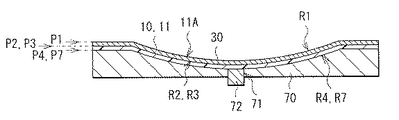
(第1の実施の形態)
図1は、本開示の第1の実施の形態に係る固体撮像装置1の断面構成を表したものである。この固体撮像装置1は、例えばデジタルスチルカメラ,ビデオカメラ等の電子機器に用いられるものであり、固体撮像素子(センサ)11を有する半導体基板10を、パッケージ20に収容した構成を有している。
(First embodiment)
FIG. 1 illustrates a cross-sectional configuration of the solid-
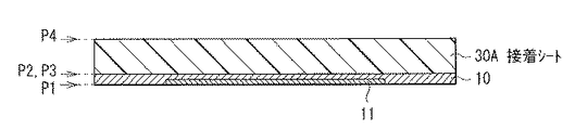
半導体基板10は、例えばシリコン(Si)ウェーハ(図示せず)から個片化された固体撮像素子11のチップである。半導体基板10は、第1面P1および第2面P2を有し、第1面P1には固体撮像素子11が設けられ、第2面P2は樹脂層30によりパッケージ21の底部21に固着されている。
The
固体撮像素子11は、第1面P1の湾曲部R1に設けられている。湾曲部R1は、固体撮像素子11の撮像面11Aを湾曲させることにより、レンズ(図示せず)の結像する像面の像面湾曲収差を低減し、良好な画像の撮像を可能とするものである。湾曲部R1は、例えば、半導体基板10の厚み方向の断面では弧状をなし、三次元的には椀状の曲面をなす凹部である。
The solid-
固体撮像素子11は、例えばCMOSイメージセンサである。固体撮像素子11の構成は特に限定されず、例えば、半導体基板10の第1面P1にフォトダイオードおよびカラーフィルタよりなる画素を2次元配置したものでもよい。また、固体撮像素子11は、例えば、一画素内に光電変換素子とフォトダイオードとが半導体基板10の厚み方向に積層され、互いに異なる波長域の光を選択的に検出して光電変換を行う、いわゆる縦方向分光型のものでもよい。いずれの場合も、固体撮像素子11は、裏面照射型でもよいし、また表面照射型でもよい。
The solid-
半導体基板10の厚みDは、例えば50μm以下であることが好ましい。半導体基板10の厚みを50μm以下と薄くするほうが、半導体基板10の応力を小さくすることが可能となり、後述する製造工程において半導体基板10を変形させやすくすることが可能となる。また、半導体基板10の厚みは、30μm以下であればより好ましく、25μm以下であれば更に好ましい。なお、半導体基板10の厚みは、少なくとも固体撮像素子11を形成可能程度でゲッタリング効果を失わないように、例えば10μm以上であることが好ましい。
The thickness D of the
パッケージ20は、半導体基板11を収容するものであり、セラミック、プラスチックなどにより構成されている。パッケージ20は、底部21に対向して開口22を有し、この開口22は封止ガラス40により封止されている。半導体基板10とパッケージ20との間には、例えば金線などのワイヤーボンドにより、ワイヤWが接続されている。
The
パッケージ20の底部21には、貫通孔23が設けられている。貫通孔23は、後述する製造方法において真空吸着の吸引孔として用いられるものである。貫通孔23は、例えば、底部21の中央に設けられていることが好ましい。
A through
樹脂層30は、半導体基板10をパッケージ20の底部21に固着させる接着層としての機能を有するものである。また、樹脂層30は、その形状を制御することにより、半導体基板10の第1面P1の湾曲部R1の湾曲形状を制御し、像面湾曲収差の高精度な補正を可能とするものである。
The
すなわち、樹脂層30は、第3面P3および第4面P4を有し、第3面P3は半導体基板10の第2面P2に接し、第4面P4はパッケージ20の底部21に接している。これにより、この固体撮像装置1では、湾曲部をもつ台座基板のような高コストな部品を設けることなく、像面湾曲収差を高い精度で補正することが可能となっている。
That is, the
樹脂層30は、Bステージ状の接着シート、例えばDAF(ダイアタッチメントフィルム)材を架橋させることにより形成されたものである。Bステージ状の接着シートは、半導体デバイスを薄くしたものを保持しつつ接着可能な、熱硬化性樹脂の反応の中間的な段階のものであって、熱によって軟化し(変形可能となり)、ある温度以上から架橋が開始される。このようなBステージ状の接着シートすなわち樹脂層30の材料としては、例えば、エポキシ系の樹脂が好ましい。また、エポキシ系のほか、アクリル系、シアン系の樹脂でもよい。
The
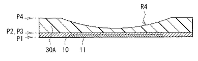
半導体基板10の第2面P2および樹脂層30の第3面P3は、それぞれ、第1面P1の湾曲部R1に倣う形状の湾曲部R2,R3を有している。樹脂層30の第4面P4は、パッケージ20の底部21の形状に倣う形状を有する。すなわち、第4面P4は平坦面である。
The second surface P2 of the
固体撮像素子11の像面湾曲収差の補正量Aは、例えば50μm以下であることが好ましい。ここに補正量Aとは、樹脂層30の第3面P3の湾曲の度合い、つまりパッケージ20の底部21からの樹脂層30の厚みの最大値と最小値との差をいう。補正量Aが50μmよりも大きい場合には、半導体基板10を構成するシリコン(Si)と、樹脂層30を構成するDAF材とのCTE(線膨張係数)の差に起因して、温度が変わると応力が発生し、湾曲部R3が変形するおそれがある。
The correction amount A of the field curvature aberration of the solid-
像面湾曲収差の補正量Aの精度は、レンズ(図示せず)の焦点深度内にあることが望ましい。補正量Aの精度がレンズの焦点深度内にない場合には、ずれている部分は画像の中でぼけてしまうからである。望ましい精度は、Fno×d×2(FnoはレンズのF値、dは固体撮像素子11の画素サイズをそれぞれ表す。)の式により与えられる。例えばレンズのF値Fnoが2.0であり、画素サイズdが2μmである場合、2×2×2=8μmで、補正量Aはプラスマイナス8μmの精度を有することが望ましい。実際には、像面収差の補正を目的としているので、補正量Aは、その4分の1程度、つまりプラスマイナス2μmの精度を有していれば、より望ましい。 The accuracy of the correction amount A of the field curvature aberration is preferably within the focal depth of a lens (not shown). This is because when the accuracy of the correction amount A is not within the focal depth of the lens, the shifted portion is blurred in the image. Desirable accuracy is given by the formula of Fno × d × 2 (Fno is the F value of the lens, and d is the pixel size of the solid-state imaging device 11). For example, when the F value Fno of the lens is 2.0 and the pixel size d is 2 μm, it is desirable that 2 × 2 × 2 = 8 μm and the correction amount A has an accuracy of plus or minus 8 μm. Actually, since the object is to correct field aberrations, it is more desirable that the correction amount A has an accuracy of about one-fourth, that is, plus or minus 2 μm.
この固体撮像装置1は、例えば、次のようにして製造することができる。
For example, the solid-
図2ないし図7は、この固体撮像装置1の製造方法を工程順に表したものである。まず、シリコンウェーハ(図示せず)の状態の半導体基板10を用意し、この半導体基板10の第1面P1に固体撮像素子11を形成し、第2面P2を研磨して半導体基板10を薄膜化する。次いで、半導体基板10をDAF材よりなるBステージの接着シート30Aに載せた状態で、固体撮像素子11を個片化する。これにより、図2に示したように、半導体基板10、すなわち個片化された固体撮像素子11のチップが形成される。
2 to 7 show the manufacturing method of the solid-
図2に示したように、半導体基板10は、第1面P1および第2面P2を有し、第1面P1に固体撮像素子11が設けられている。接着シート30Aは、第3面P3および第4面P4を有している。半導体基板10と接着シート30Aとは、第2面P2と第3面P3とを接触させて配置されている。
As shown in FIG. 2, the
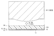
次いで、図3に示したように、接着シート30Aが架橋しないで変形可能な温度の熱H1をかけながら、接着シート30Aの第4面P4に凸金型50を接触させて圧力Pをかけて、接着シート30Aの変形を行い、冷却する。これにより、図4に示したように、接着シート30Aの第4面P4に湾曲部R4を形成する。
Next, as shown in FIG. 3, while applying heat H1 at a temperature at which the
そののち、図5に示したように、底部21に貫通孔23を有するパッケージ20を用意し、このパッケージ20に、半導体基板10および接着シート30Aを表裏反転させて収容する。これにより、第4面P4の湾曲部R4とパッケージ20の底部21との間に空洞Gが形成される。空洞Gは、貫通孔23を介して外部の大気と連通されている。
After that, as shown in FIG. 5, a
続いて、図6に示したように、空洞Gの内外に圧力差を設けることにより、半導体基板10および接着シート30Aを変形させて空洞Gを除去し、半導体基板10の第1面P1に湾曲部R1を形成する。接着シート30Aの第4面P4は、パッケージ20の底部21に接触する。
Subsequently, as shown in FIG. 6, by providing a pressure difference inside and outside the cavity G, the
具体的には、図5に示したように、熱H2をかけながら貫通孔23を用いて真空吸着VAを行うことで、空洞Gを真空にすると共に半導体基板10および接着シート30Aに大気圧APをかけて、半導体基板10および接着シート30Aを変形させて空洞Gを除去する。なお、熱H2は比較的低温とし、接着シート30Aを過度に変形させないようにすることが好ましい。このようにすることにより、図6に示したように、半導体基板の第1面P1に、元の湾曲部R4の形状を高精度に反映した湾曲部R1を形成することが可能となる。
Specifically, as shown in FIG. 5, by performing vacuum suction VA using the through-
そののち、接着シート30Aを架橋温度以上に加熱することにより、接着シート30Aを架橋させて樹脂層30を形成する。これにより、半導体基板10が樹脂層30によりパッケージ20の底部21に固着される。
After that, the
最後に、図7に示したように、半導体基板10とパッケージ20との間に、ワイヤボンディングによりワイヤWを接続し、パッケージ20の開口22を封止ガラス40で封止する。以上により、図1に示した固体撮像装置1が完成する。
Finally, as shown in FIG. 7, a wire W is connected between the
この固体撮像装置1では、半導体基板10の第1面P1の湾曲部R1に固体撮像素子11が設けられているので、固体撮像素子11の撮像面11Aは湾曲している。よって、レンズ(図示せず)の結像する像面の像面湾曲収差が解消され、良好な画像の撮像が可能となる。
In the solid-
ここでは、半導体基板10とパッケージ20との間に樹脂層30が設けられ、樹脂層30の第3面P3は半導体基板10の第2面P2に接し、第4面P4はパッケージ20の底部21に接している。よって、樹脂層30の湾曲形状を制御することにより、像面湾曲収差が高い精度で補正される。
Here, the
このように本実施の形態では、半導体基板10とパッケージ20との間に樹脂層30を設け、樹脂層30の第3面P3を半導体基板10の第2面P2に接触させ、第4面P4をパッケージ20の底部21に接触させるようにしたので、像面湾曲収差を高い精度で補正することが可能となる。
Thus, in the present embodiment, the
(第2の実施の形態)
図8は、本開示の第2の実施の形態に係る固体撮像装置1Aの断面構成を表したものである。この固体撮像装置1Aは、パッケージ20の底部21に貫通孔23が設けられておらず、底部21が空間的に連続した部材により構成されていることを除いては、上記第1の実施の形態と同様の構成、作用および効果を有している。よって、対応する構成要素には同一の符号を付して説明する。
(Second Embodiment)
FIG. 8 illustrates a cross-sectional configuration of a solid-
本実施の形態では、上述したように、パッケージ20の底部21に貫通孔23がなく、空間的に連続した部材により構成されている。従って、貫通孔23からの水分の浸入に起因する剥がれなどが抑えられ、固体撮像素子11の信頼性が向上する。また、撮像したときに、光の状態により、固体撮像素子11の撮像面11Aに貫通孔23が映り込んでしまうおそれを小さくすることが可能となる。なお、貫通孔23からの水分の浸入は、製造工程の最終段階で貫通孔23を塞いでおくことにより回避することも可能である。
In the present embodiment, as described above, the
この固体撮像装置1Aは、例えば、次のようにして製造することができる。
This solid-
図9ないし図11は、この固体撮像素子10Aの製造方法を工程順に表したものである。なお、第1の実施の形態と重複する工程については、図2ないし図4、および図7を参照して説明する。 9 to 11 show the manufacturing method of the solid-state imaging device 10A in the order of steps. In addition, the process which overlaps with 1st Embodiment is demonstrated with reference to FIG. 2 thru | or 4 and FIG.
まず、第1の実施の形態と同様にして、図2に示した工程により、半導体基板10と、接着シート30Aとを、第2面P2と第3面P3とを接触させて配置する。半導体基板10は、第1面P1および第2面P2を有し、第1面P1に固体撮像素子11が設けられている。接着シート30Aは、第3面P3および第4面P4を有している。
First, similarly to the first embodiment, the
次いで、第1の実施の形態と同様にして、図3および図4に示した工程により、加熱H1および凸金型50を用いた加圧Pにより、接着シート30Aの第4面P4に湾曲部R4を形成する。
Next, in the same manner as in the first embodiment, the curved portion is formed on the fourth surface P4 of the
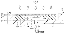
続いて、図9に示したように、チャンバー構造を持つ実装装置を用い、チャンバー60内に、底部21が空間的に連続した部材よりなるパッケージ20を設置し、パッケージ20の上方に、半導体基板10および接着シート30Aを表裏反転させて保持し、チャンバー60内の真空排気Eを行う。
Subsequently, as shown in FIG. 9, using a mounting apparatus having a chamber structure, a
そののち、図10に示したように、半導体基板10および接着シート30Aを、真空V中で、パッケージ20に収容する。これにより、第4面P4の湾曲部R4とパッケージ20の底部21との間に、真空Vの空洞Gが形成される。
After that, as shown in FIG. 10, the
続いて、図11に示したように、大気解放ARにより半導体基板10および接着シート30Aに大気圧APをかけて、半導体基板10および接着シート30Aを変形させて空洞Gを除去し、半導体基板10の第1面P1に湾曲部R1を形成する。接着シート30Aの第4面P4は、パッケージ20の底部21に接触する。
Subsequently, as shown in FIG. 11, atmospheric pressure AP is applied to the
具体的には、図10に示したように、熱H2をかけながらチャンバー60を大気解放し、空洞Gの内部の負圧を利用して半導体基板10および接着シート30Aに大気圧APをかける。その際の大気圧APのかけ方を適切に制御することにより、半導体基板10および接着シート30Aを変形させて空洞Gを除去する。なお、熱H2は比較的低温とし、接着シート30Aを過度に変形させないようにすることが好ましい。このようにすることにより、図11に示したように、半導体基板の第1面P1に、元の湾曲部R4の形状を高精度に反映した湾曲部R1を形成することが可能となる。
Specifically, as shown in FIG. 10, the
そののち、接着シート30Aを架橋温度以上に加熱することにより、接着シート30Aを架橋させて樹脂層30を形成する。これにより、半導体基板10が樹脂層30によりパッケージ20の底部21に固着される。
After that, the
最後に、第1の実施の形態と同様にして、図7に示した工程により、半導体基板10とパッケージ20との間に、ワイヤボンディングによりワイヤWを接続し、パッケージ20の開口22を封止ガラス40で封止する。以上により、図8に示した固体撮像装置1Aが完成する。
Finally, similarly to the first embodiment, the wire W is connected by wire bonding between the
この固体撮像装置1Aでは、第1の実施の形態と同様に、半導体基板10の第1面P1の湾曲部R1に固体撮像素子11が設けられているので、固体撮像素子11の撮像面11Aは湾曲している。よって、レンズ(図示せず)の結像する像面の像面湾曲収差が解消され、良好な画像の撮像が可能となる。
In the solid-
また、半導体基板10とパッケージ20との間に樹脂層30が設けられ、樹脂層30の第3面P3は半導体基板10の第2面P2に接し、第4面P4はパッケージ20の底部21に接している。よって、樹脂層30の湾曲形状を制御することにより、像面湾曲収差が高い精度で補正される。
A
更に、パッケージ20の底部21が、空間的に連続した部材により構成されている、つまり底部21に貫通孔23が設けられていない。従って、貫通孔23からの水分の浸入に起因する剥がれなどが抑えられ、固体撮像素子11の信頼性が向上する。また、撮像したときに、光の状態により、固体撮像素子11の撮像面11Aに貫通孔23が映り込んでしまうおそれが小さくなる。
Further, the
このように本実施の形態では、第1の実施の形態と同様に、半導体基板10とパッケージ20との間に樹脂層30を設け、樹脂層30の第3面P3を半導体基板10の第2面P2に接触させ、第4面P4をパッケージ20の底部21に接触させるようにしたので、像面湾曲収差を高い精度で補正することが可能となる。
Thus, in the present embodiment, as in the first embodiment, the
また、パッケージ20の底部21に貫通孔23を設けず、空間的に連続した部材により構成するようにしたので、貫通孔23からの水分の浸入に起因する剥がれなどを抑え、固体撮像素子11の信頼性を高めることが可能となる。また、撮像したときに、光の状態により、固体撮像素子11の撮像面11Aに貫通孔23が映り込んでしまうおそれを小さくし、撮像品質の向上が可能となる。
In addition, since the through
(第3の実施の形態)
図12は、本開示の第3の実施の形態に係る固体撮像装置1Bの断面構成を表したものである。上記第1の実施の形態では、樹脂層30の形状を制御することにより、半導体基板10の第1面P1の湾曲部R1の湾曲形状を制御するのに対して、本実施の形態は、半導体基板10自体の形状を制御することにより、半導体基板10の第1面P1の湾曲部R1の湾曲形状を制御し、像面湾曲収差の高精度な補正を可能とするようにしたものである。このことを除いては、この固体撮像装置1Bは、上記第1の実施の形態と同様の構成を有している。
(Third embodiment)
FIG. 12 illustrates a cross-sectional configuration of a solid-state imaging device 1B according to the third embodiment of the present disclosure. In the first embodiment, the curved shape of the curved portion R1 of the first surface P1 of the
この固体撮像装置1Bでは、半導体基板10の第1面P1は湾曲部R1を有し、半導体基板10の第2面P2と樹脂層30の第3面P3および第4面P4は、パッケージ20の底部21に倣う形状を有する、つまり平坦面となっている。
In the solid-state imaging device 1B, the first surface P1 of the
固体撮像素子11の像面湾曲収差の補正量Aは、第1の実施の形態と同様に、例えば50μm以下であることが好ましい。本実施の形態において、補正量Aは、半導体基板10の第1面P1の湾曲部R1の湾曲の度合い、つまり半導体基板10の厚みの最大値と最小値との差をいう。補正量Aが50μmよりも大きい場合には、半導体基板10を構成するシリコン(Si)と、樹脂層30を構成するDAF材とのCTE(線膨張係数)の差に起因して、温度が変わると応力が発生し、湾曲部R3が変形するおそれがある。
The correction amount A of the field curvature aberration of the solid-
この固体撮像装置1Bは、例えば次のようにして製造することができる。 This solid-state imaging device 1B can be manufactured as follows, for example.
図13ないし図16は、この固体撮像装置1Bの製造方法を工程順に表したものである。本実施の形態の製造方法は、接着シート30Aの第4面P4に湾曲部R4を形成する方法において上記第1の実施の形態の製造方法とは異なるものである。すなわち、上記第1の実施の形態では、凸金型50を用いて接着シート30Aの第4面P4に湾曲部R4を形成するようにしている。一方、本実施の形態では、半導体基板10の第2面P2にエッチングにより湾曲部R2を形成しておき、この湾曲部R2に沿わせて接着シート30Aを貼り合わせることにより、接着シート30Aの第4面P4に、湾曲部R2の形状を反映した湾曲部R4を形成するようにしている。
13 to 16 show the manufacturing method of the solid-state imaging device 1B in the order of steps. The manufacturing method of the present embodiment is different from the manufacturing method of the first embodiment in the method of forming the curved portion R4 on the fourth surface P4 of the
まず、シリコンウェーハ(図示せず)の状態の半導体基板10を用意し、この半導体基板10の第1面P1に固体撮像素子11を形成し、第2面P2を研磨して半導体基板10を薄膜化する。次いで、図13に示したように、グラデーションマスクを用いた三次元エッチングにより第2面P2に湾曲部R2を形成する。
First, the
続いて、半導体基板10をDAF材よりなるBステージの接着シート30Aに載せた状態で、固体撮像素子11を個片化する。これにより、図14に示したように、半導体基板10、すなわち個片化された固体撮像素子11のチップが形成される。
Subsequently, the solid-
図14に示したように、半導体基板10は、第1面P1および第2面P2を有し、第1面P1に固体撮像素子11が設けられ、第2面P2に湾曲部R2が設けられている。接着シート30Aは、第3面P3および第4面P4を有している。半導体基板10と接着シート30Aとは、第2面P2と第3面P3とを接触させて配置されている。接着シート30Aの第3面P3および第4面P4には、湾曲部R2の形状に倣って、湾曲部R3,R4が形成されている。
As shown in FIG. 14, the
そののち、図15に示したように、底部21に貫通孔23を有するパッケージ20を用意し、このパッケージ20に、半導体基板10および接着シート30Aを表裏反転させて収容する。このとき、第4面P4の湾曲部R4とパッケージ20の底部21との間に空洞Gが形成される。空洞Gは、貫通孔23を介して外部の大気と連通されている。
After that, as shown in FIG. 15, a
続いて、図16に示したように、空洞Gの内外に圧力差を設けることにより、半導体基板10および接着シート30Aを変形させて空洞Gを除去し、半導体基板10の第1面P1に湾曲部R1を形成する。接着シート30Aの第4面P4は、パッケージ20の底部21に接触する。
Subsequently, as shown in FIG. 16, by providing a pressure difference between the inside and outside of the cavity G, the
具体的には、図15に示したように、熱H2をかけながら貫通孔23を用いて真空吸着VAを行うことで、空洞Gを真空にすると共に半導体基板10および接着シート30Aに大気圧APをかけて、半導体基板10および接着シート30Aを変形させて空洞Gを除去する。なお、熱H2は比較的低温とし、接着シート30Aを過度に変形させないようにすることが好ましい。このようにすることにより、図16に示したように、半導体基板の第1面P1に、元の湾曲部R4の形状を高精度に反映した湾曲部R1を形成することが可能となる。
Specifically, as shown in FIG. 15, by performing vacuum suction VA using the through
そののち、接着シート30Aを架橋温度以上に加熱することにより、接着シート30Aを架橋させて樹脂層30を形成する。これにより、半導体基板10が樹脂層30によりパッケージ20の底部21に固着される。
After that, the
最後に、図12に示したように、半導体基板10とパッケージ20との間に、ワイヤボンディングによりワイヤWを接続し、パッケージ20の開口22を封止ガラス40で封止する。以上により、図12に示した固体撮像装置1Bが完成する。
Finally, as shown in FIG. 12, a wire W is connected between the
この固体撮像装置1Bの作用および効果は第1の実施の形態と同様である。 The operations and effects of the solid-state imaging device 1B are the same as those in the first embodiment.
(変形例1)
なお、この固体撮像装置1Bでは、図17に示したように、第2の実施の形態と同様に、パッケージ20の底部21に貫通孔23を設けず、空間的に連続した部材により構成することも可能である。その場合の製造方法は、第2の実施の形態と同様である。これにより第1の実施の形態の効果に加えて第2の実施の形態と同様の作用・効果を得ることも可能である。
(Modification 1)
As shown in FIG. 17, the solid-
(第4の実施の形態)
図18は、本開示の第4の実施の形態に係る固体撮像装置1Cの断面構成を表したものである。この固体撮像装置1Cは、樹脂層30を、第1樹脂層31および第2樹脂層32の2層構造とし、第1樹脂層31の形状を制御することにより、半導体基板10の第1面P1の湾曲部R1の湾曲形状を制御し、像面湾曲収差の高精度な補正を可能とするようにしたものである。このことを除いては、この固体撮像装置1Cは、上記第1の実施の形態と同様の構成を有している。
(Fourth embodiment)
FIG. 18 illustrates a cross-sectional configuration of a solid-state imaging device 1C according to the fourth embodiment of the present disclosure. In the solid-
本実施の形態では、上述したように、樹脂層30は、第1樹脂層31および第2樹脂層32の2層構造を有している。第1樹脂層31は、樹脂層30において半導体基板10側に設けられ、第3面P3および第5面P5を有している。第2樹脂層32は、樹脂層30においてパッケージ20側に設けられ、第6面P6および第4面P4を有している。第2樹脂層32は、Bステージ状の接着シート30A、例えばDAF材を架橋させることにより形成されたものである。
In the present embodiment, as described above, the
半導体基板10の第2面P2と第1樹脂層31の第3面P3とは、それぞれ湾曲部R2,R3を有している。第1樹脂層31の第5面P5と第2樹脂層32の第6面P6および第4面P4は、パッケージ20の底部21に倣う形状を有する、すなわち平坦面となっている。
The second surface P2 of the
固体撮像素子11の像面湾曲収差の補正量Aは、第1の実施の形態と同様に、例えば50μm以下であることが好ましい。本実施の形態において、補正量Aは、第1樹脂層31の第3面P3の湾曲部R3の湾曲の度合い、つまり第1樹脂層31の厚みの最大値と最小値との差をいう。補正量Aが50μmよりも大きい場合には、半導体基板10を構成するシリコン(Si)と、第1樹脂層31または第2樹脂層32の材料とのCTE(線膨張係数)の差に起因して、温度が変わると応力が発生し、湾曲部R3が変形するおそれがある。
The correction amount A of the field curvature aberration of the solid-
この固体撮像装置1Cは、例えば次のようにして製造することができる。 The solid-state imaging device 1C can be manufactured, for example, as follows.
図19ないし図22は、この固体撮像装置1Cの製造方法を工程順に表したものである。本実施の形態の製造方法は、接着シート30Aの第4面P4に湾曲部R4を形成する方法において上記第1の実施の形態の製造方法とは異なるものである。すなわち、上記第1の実施の形態では、凸金型50を用いて接着シート30Aの第4面P4に湾曲部R4を形成するようにしている。一方、本実施の形態では、第1樹脂層31の第5面P5にナノインプリントにより湾曲部R5を形成しておき、この湾曲部R5に沿わせて接着シート30Aを貼り合わせることにより、接着シート30Aの第4面P4に、湾曲部R5の形状を反映した湾曲部R4を形成するようにしている。
19 to 22 show the manufacturing method of the solid-state imaging device 1C in the order of steps. The manufacturing method of the present embodiment is different from the manufacturing method of the first embodiment in the method of forming the curved portion R4 on the fourth surface P4 of the
まず、シリコンウェーハ(図示せず)の状態の半導体基板10を用意し、この半導体基板10の第1面P1に固体撮像素子11を形成し、第2面P2を研磨して半導体基板10を薄膜化する。次いで、図19に示したように、この半導体基板10の第2面P2に、ナノインプリント法により、第1樹脂層31を形成する。第1樹脂層31は、第3面P3および第5面P5を有し、第3面は半導体基板10の第2面P2に接し、第5面P5には湾曲部R5が設けられている。
First, the
具体的には、半導体基板10の第2面P2に、紫外線硬化型樹脂よりなる樹脂層(図示せず)を形成し、この樹脂層を金型(図示せず)に接触させて紫外光を照射したのち、金型から離型する。これにより、第5面P5に湾曲部R5を有する第1樹脂層31が形成される。
Specifically, a resin layer (not shown) made of an ultraviolet curable resin is formed on the second surface P2 of the
続いて、半導体基板10をDAF材よりなるBステージの接着シート30Aに載せた状態で、固体撮像素子11を個片化する。これにより、図20に示したように、半導体基板10、すなわち個片化された固体撮像素子11のチップが形成される。
Subsequently, the solid-
図20に示したように、接着シート30Aは、第6面P6および第4面P4を有している。第1樹脂層31と、接着シート30Aとは、第5面P5と第6面P6とを接触させて配置されている。これにより、接着シート30Aの第4面P4には、湾曲部R5の形状に倣って、湾曲部R4が形成されている。
As shown in FIG. 20, the
そののち、図21に示したように、底部21に貫通孔23を有するパッケージ20を用意し、このパッケージ20に、半導体基板10および接着シート30Aを表裏反転させて収容する。このとき、第4面P4の湾曲部R4とパッケージ20の底部21との間に空洞Gが形成される。空洞Gは、貫通孔23を介して外部の大気と連通されている。
After that, as shown in FIG. 21, a
続いて、図22に示したように、空洞Gの内外に圧力差を設けることにより、半導体基板10および接着シート30Aを変形させて空洞Gを除去し、半導体基板10の第1面P1に湾曲部R1を形成する。接着シート30Aの第4面P4は、パッケージ20の底部21に接触する。
Subsequently, as shown in FIG. 22, by providing a pressure difference inside and outside the cavity G, the
具体的には、図21に示したように、熱H2をかけながら貫通孔23を用いて真空吸着VAを行うことで、空洞Gを真空にすると共に半導体基板10および接着シート30Aに大気圧APをかけて、半導体基板10および接着シート30Aを変形させて空洞Gを除去する。なお、熱H2は比較的低温とし、接着シート30Aを過度に変形させないようにすることが好ましい。このようにすることにより、図22に示したように、半導体基板の第1面P1に、元の湾曲部R4の形状を高精度に反映した湾曲部R1を形成することが可能となる。
Specifically, as shown in FIG. 21, by performing vacuum suction VA using the through
そののち、接着シート30Aを架橋温度以上に加熱することにより、接着シート30Aを架橋させて樹脂層30を形成する。これにより、半導体基板10が樹脂層30によりパッケージ20の底部21に固着される。
After that, the
最後に、図18に示したように、半導体基板10とパッケージ20との間に、ワイヤボンディングによりワイヤWを接続し、パッケージ20の開口22を封止ガラス40で封止する。以上により、図18に示した固体撮像装置1Cが完成する。
Finally, as shown in FIG. 18, a wire W is connected between the
この固体撮像装置1Cの作用および効果は第1の実施の形態と同様である。 The operation and effect of the solid-state imaging device 1C are the same as those in the first embodiment.
(変形例2)
なお、この固体撮像装置1Cでは、図23に示したように、第2の実施の形態と同様に、パッケージ20の底部21に貫通孔23を設けず、空間的に連続した部材により構成することも可能である。その場合の製造方法は、第2の実施の形態と同様である。これにより第1の実施の形態の効果に加えて第2の実施の形態と同様の作用・効果を得ることも可能である。
(Modification 2)
In the solid-state imaging device 1C, as shown in FIG. 23, similarly to the second embodiment, the through
(第5の実施の形態)
図24は、本開示の第5の実施の形態に係る固体撮像装置1Dの断面構成を表したものである。この固体撮像装置1Dは、例えば、固体撮像素子11を有する半導体基板10を樹脂層30により保持部材(台座)70に保持させて、パッケージ20に収容した構成を有している。以下、第1の実施の形態と同一の構成要素には同一の符号を付して説明する。
(Fifth embodiment)
FIG. 24 illustrates a cross-sectional configuration of a solid-state imaging device 1D according to the fifth embodiment of the present disclosure. The solid-state imaging device 1D has a configuration in which, for example, the
半導体基板10は、第1の実施の形態と同様に、例えばシリコン(Si)ウェーハ(図示せず)から個片化された固体撮像素子11のチップである。半導体基板10は、第1面P1および第2面P2を有し、第1面P1には固体撮像素子11が設けられ、第2面P2は樹脂層30に接合されている。
As in the first embodiment, the
固体撮像素子11は、第1の実施の形態と同様に、第1面P1の湾曲部R1に設けられたCMOSイメージセンサである。湾曲部R1は、第1の実施の形態と同様に、半導体基板10の厚み方向の断面では弧状をなし、三次元的には椀状の曲面をなしている。固体撮像素子11の構成については、第1の実施の形態と同様である。
The solid-
パッケージ20は、底部21の貫通孔23を有しないことを除いては、第1の実施の形態と同様に構成されている。封止ガラス40およびワイヤWは、第1の実施の形態と同様に構成されている。
The
樹脂層30は、半導体基板10を保持部材70に固着させる接着層としての機能を有するものである。樹脂層30の第3面P3は、半導体基板10の第2面P2に接合されている。樹脂層30の第4面P4は、保持部材70の上面P7に接合されている。樹脂層30は、第1の実施の形態と同様に、Bステージ状の接着シート、例えばDAF材を架橋させることにより形成されたものである。樹脂層30の材料は、第1の実施の形態と同様である。
The
保持部材70は、半導体基板10を保持すると共に、半導体基板10の第1面P1の湾曲部R1の湾曲形状を制御し、像面湾曲収差を補正するものであり、例えばシリコン(Si)、樹脂、金属、セラミックにより構成されている。保持部材70は、上面P7に湾曲部R7を有している。この湾曲部R7は、保持部材70の厚み方向の断面では弧状をなし、三次元的には椀状の曲面をなしている。これにより、半導体基板10の第1面P1および第2面P2と、樹脂層30の第3面P3および第4面P4とには、保持部材70の上面P7の湾曲部R7に倣う形状の湾曲部R1,R2,R3,R4がそれぞれ形成されている。
The holding
また、保持部材70には、貫通孔71が設けられている。貫通孔71は、後述する製造方法において真空吸着の吸引孔として用いられるものである。貫通孔71は、例えば、保持部材70の椀状の三次元曲面の中央に設けられていることが好ましい。
Further, the holding
貫通孔71は、保持部材70と同じ反射率をもつ材料よりなる埋込み層72で埋め込まれていることが好ましい。これにより、貫通孔71に起因する固体撮像素子11の面内出力差を低減し、画像のムラを抑えることが可能となる。
The through
この固体撮像装置1Dは、例えば、次のようにして製造することができる。 This solid-state imaging device 1D can be manufactured as follows, for example.
図25ないし図29は、この固体撮像装置1Dの製造方法を工程順に表したものである。なお、第1の実施の形態と重複する工程については、図2を参照して説明する。 25 to 29 show the manufacturing method of the solid-state imaging device 1D in the order of steps. In addition, the process which overlaps with 1st Embodiment is demonstrated with reference to FIG.
まず、第1の実施の形態と同様にして、図2に示した工程により、半導体基板10の第1面P1に固体撮像素子11を形成し、第2面P2を研磨して半導体基板10を薄膜化する。次いで、同じく図2に示した工程により、半導体基板10をDAF材よりなるBステージの接着シート30Aに乗せた状態で、固体撮像素子11を個片化する。
First, similarly to the first embodiment, the solid-
続いて、図25に示したように、半導体基板10および接着シート30Aを、保持部材70の上面P7に設置する。接着シート30Aの第4面P4は、保持部材70の上面P7の周縁部のみに接し、接着シート30Aの第4面P4と保持部材70の上面P7の湾曲部R7との間には、空洞Gが生じている。空洞Gは、保持部材70の貫通孔71を介して外部の大気と連通されている。
Subsequently, as illustrated in FIG. 25, the
そののち、図26に示したように、半導体基板10、接着シート30Aおよび保持部材70を図示しないチャンバー内に設置して真空排気Eを行う。これにより、空洞Gの内外に圧力差が生じ、半導体基板10および接着シート30Aが変形して空洞Gが除去される。
After that, as shown in FIG. 26, the
このようにして、図27に示したように、接着シート30Aの第4面P4が保持部材70の上面P7に接触する。半導体基板10の第1面P1および第2面P2と、接着シート30Aの第3面P3および第4面P4とには、保持部材70の上面P7の湾曲部R7の形状に倣う湾曲部R1,R2,R3,R4がそれぞれ形成される。
In this way, the fourth surface P4 of the
続いて、接着シート30Aを架橋温度以上に加熱することにより、接着シート30Aを架橋させて樹脂層30を形成する。これにより、半導体基板10が樹脂層30により保持部材70の上面P7に固着される。
Subsequently, the
続いて、図28に示したように、保持部材70の貫通孔71に、保持部材70と同じ反射率をもつ材料よりなる埋込み層72を形成する。そののち、図29に示したように、研磨などの平坦化を行い、埋込み層72の貫通孔71から突出した部分を除去する。
Subsequently, as shown in FIG. 28, a buried
最後に、図24に示したように、保持部材70をパッケージ20に収容し、半導体基板10とパッケージ20との間に、ワイヤボンディングによりワイヤWを接続し、パッケージ20の開口22を封止ガラス40で封止する。以上により、図24に示した固体撮像装置1Dが完成する。
Finally, as shown in FIG. 24, the holding
この固体撮像装置1Dでは、第1の実施の形態と同様に、半導体基板10の第1面P1の湾曲部R1に固体撮像素子11が設けられているので、固体撮像素子11の撮像面11Aは湾曲している。よって、レンズ(図示せず)の結像する像面の像面湾曲収差が解消され、良好な画像の撮像が可能となる。
In the solid-state imaging device 1D, as in the first embodiment, since the solid-
また、このとき、入射光h1は、図30に示したように、半導体基板10および樹脂層30を通過し、保持部材70の上面P7で反射されて反射光h2が生じる。また、貫通孔71には埋込み層72が設けられているので、入射光h1は、図31に示したように、半導体基板10および樹脂層30を通過し、埋込み層72で反射されて反射光h3が生じる。埋込み層72は保持部材70と同じ反射率をもつ材料よりなるので、反射光h2,h3の光量は同等になる。よって、固体撮像素子11の貫通孔71上の部分とそれ以外の部分で出力差がなくなり、画像のムラが解消される。
At this time, as shown in FIG. 30, the incident light h1 passes through the
このように本実施の形態では、半導体基板10を樹脂層30により保持部材70に保持させてパッケージ20に収容し、保持部材70の貫通孔71を保持部材70と同じ反射率の埋込み層72で埋めるようにしたので、貫通孔71に起因する固体撮像素子11の面内出力差を低減し、画像のムラを抑えることが可能となる。
Thus, in the present embodiment, the
なお、上記実施の形態では、図24に示したように、貫通孔71の径φが貫通孔71の長手方向で等しい場合について説明した。しかしながら、図32に示したように、貫通孔71のパッケージ20側の開口径φAが、貫通孔71の半導体基板10側の開口径φBよりも大きいようにすることが好ましい。これにより、貫通孔71に埋込み層72を埋め込みやすくすることが可能となる。
In the above embodiment, as shown in FIG. 24, the case where the diameter φ of the through
また、上記実施の形態では、図24に示したように、貫通孔71が固体撮像素子11の撮像面11Aの法線Nに平行に、パッケージ20の底部21に対して垂直に設けられている場合について説明した。しかしながら、図33に示したように、貫通孔71は、固体撮像素子11の撮像面11Aの法線方向Nに対して斜めに設けられていてもよい。あるいは、図34に示したように、貫通孔71は、半導体基板10側の開口71Bとパッケージ20側の開口71Aとの間に屈曲部71Cを有していてもよい。このようにすることにより、固体撮像素子11の面内方向において開口71A,71Bの位置が異なり、貫通孔71に起因する固体撮像素子11の面内出力差を低減し、画像のムラを抑えることが可能となる。
In the above embodiment, as shown in FIG. 24, the through
更に、上記実施の形態では、図24に示したように、貫通孔71の内部に保持部材70と同じ反射率をもつ材料よりなる埋込み層72を埋め込む場合について説明した。しかしながら、パッケージ20のうち貫通孔71が位置する領域を、保持部材70と同じ反射率をもつ材料により構成してもよい。例えば図35に示したように、パッケージ20の底部21の上面に、保持部材70と同じ反射率をもつ材料よりなる上面層24を設けるようにしてもよい。これにより貫通孔71の底部が保持部材70と同じ反射率をもつ上面層24で塞がれるので、垂直光成分の反射率が同等になり、貫通孔71に起因する固体撮像素子11の面内出力差を低減し、画像のムラを抑えることが可能となる。
Furthermore, in the above embodiment, as shown in FIG. 24, the case where the embedded
加えて、本実施の形態は、第1ないし第4の実施の形態と組み合わせることも可能である。例えば、第1の実施の形態において、パッケージ20の貫通孔23に、パッケージ20と同じ反射率の埋込み層(図示せず)を設けるようにしてもよい。これにより、本実施の形態と同様に、貫通孔23に起因する固体撮像素子11の面内出力差を低減し、画像のムラを抑えることが可能となる。
In addition, this embodiment can be combined with the first to fourth embodiments. For example, in the first embodiment, an embedded layer (not shown) having the same reflectance as that of the
なお、貫通孔71に埋込み層72を設けず、貫通孔71の半導体基板10側の開口径φAを固体撮像素子11の一画素程度のサイズにするようにしてもよい。このようにすれば、出力差を生む範囲が一画素程度となるので、この画素を画像処理部(図示せず)において補正の対象とすることにより、画像のムラを抑えることが可能となる。
The embedded
また、上記実施の形態では、樹脂層30をBステージ状の接着シート、例えばDAF材を架橋させたものにより構成した場合について説明した。更に、樹脂層30を、遮光性のあるDAF材を架橋させたものにより構成することが好ましい。これにより、反射光を低減し、出力差を抑えて、画像のムラを解消することが可能となる。上記第1ないし第4の実施の形態において樹脂層30を、遮光性のあるDAF材を架橋させたものにより構成した場合も、同様の効果を得ることが可能となる。
Moreover, in the said embodiment, the case where the
遮光性をもつDAF材としては、例えば、DAF材中に近赤外領域の光を吸収する材料を混ぜ込んだもの、または、DAF材に近赤外領域の光を吸収する材料を挟んだものが挙げられる。近赤外領域の光を吸収する材料としては、例えば、カーボン、ITOあるいはATOの微粒子、または近赤外吸収色素が挙げられる。 As a DAF material having a light shielding property, for example, a DAF material mixed with a material that absorbs light in the near-infrared region, or a material that absorbs light in the near-infrared region between the DAF material. Is mentioned. Examples of the material that absorbs light in the near infrared region include carbon, ITO, or ATO fine particles, or a near infrared absorbing dye.
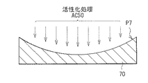
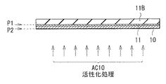
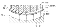
(第6の実施の形態)
図36は、本開示の第6の実施の形態に係る固体撮像装置1Eの断面構成を表したものである。この固体撮像装置1Eは、例えば、固体撮像素子11を有する半導体基板10を、樹脂層30や接着剤等を挟まずに、保持部材70に直接接合させて、パッケージ20に収容した構成を有している。以下、第1または第5の実施の形態と同一の構成要素には同一の符号を付して説明する。
(Sixth embodiment)
FIG. 36 illustrates a cross-sectional configuration of a solid-state imaging apparatus 1E according to the sixth embodiment of the present disclosure. The solid-state imaging device 1E has a configuration in which, for example, the
半導体基板10は、第1の実施の形態と同様に、例えばシリコン(Si)ウェーハ(図示せず)から個片化された固体撮像素子11のチップである。半導体基板10は、第1面P1および第2面P2を有し、第1面P1には固体撮像素子11が設けられている。第2面P2は、樹脂層30や接着剤等を挟まずに、保持部材70に直接接合されている。これにより、この固体撮像装置1Eでは、固体撮像素子11からの熱を保持部材70側に効率よく逃がし、熱によるデバイス特性低下を抑えることが可能となっている。また、半導体基板10と保持部材70との界面での反射が抑えられ、画質の向上が可能となる。
As in the first embodiment, the
パッケージ20は、底部21の貫通孔23を有しないことを除いては、第1の実施の形態と同様に構成されている。封止ガラス40およびワイヤWは、第1の実施の形態と同様に構成されている。パッケージ20に貫通孔23が設けられていないので、貫通孔23に起因する固体撮像素子11の面内出力差を低減し、画像のムラを抑えることが可能となっている。
The
保持部材70は、半導体基板10を保持すると共に、半導体基板10の第1面P1の湾曲部R1の湾曲形状を制御し、像面湾曲収差を補正するものである。保持部材70は、上面R7に湾曲部R7を有している。この湾曲部R7は、保持部材70の厚み方向の断面では弧状をなし、三次元的には椀状の曲面をなしている。これにより、半導体基板10の第1面P1および第2面P2には、保持部材70の上面P7の湾曲部R7に倣う形状の湾曲部R1,R2,R3,R4がそれぞれ形成されている。また、保持部材70には、貫通孔71は設けられていない。従って、貫通孔71に起因する固体撮像素子11の面内出力差を低減し、画像のムラを抑えることが可能となっている。
The holding
保持部材70は、半導体基板10と同等以上の熱伝導率を有することが好ましく、例えばシリコン(Si)により構成されていることが好ましい。これにより、放熱特性を高めることが可能となる。
The holding
この固体撮像装置1Eは、例えば、次のようにして製造することができる。 This solid-state imaging device 1E can be manufactured as follows, for example.
図37ないし図42は、この固体撮像装置1Eの製造方法を工程順に表したものである。なお、第1の実施の形態と重複する工程については、図2を参照して説明する。 37 to 42 show the manufacturing method of the solid-state imaging device 1E in the order of steps. In addition, the process which overlaps with 1st Embodiment is demonstrated with reference to FIG.
まず、図37に示したように、シリコン(Si)よりなると共に上面P7に湾曲部R7を有する保持部材70を用意し、この保持部材70の上面P7に対して、プラズマまたはイオンビームを用いて活性化処理AC50を行う。
First, as shown in FIG. 37, a holding
また、第1の実施の形態と同様にして、図2に示した工程により、半導体基板10の第1面P1に固体撮像素子11を形成し、第2面P2を研磨して半導体基板10を薄膜化する。次いで、同じく図2に示した工程により、半導体基板10をDAF材よりなるBステージの接着シート30Aに乗せた状態で、固体撮像素子11を個片化する。
Similarly to the first embodiment, the solid-
続いて、図38に示したように、半導体基板10の第1面P1つまり固体撮像素子11が形成されている面に、保護テープ11Bをラミネートし、保護シート30Aを剥離する。
Subsequently, as shown in FIG. 38, the
そののち、図39に示したように、半導体基板10の第2面P2に対して、プラズマまたはイオンビームを用いて活性化処理AC10を行い、半導体基板10の第2面P2を酸化する。半導体基板10の第2面P2の酸化方法は、表面保護に影響しない酸化方法であればどのような方法でもよい。
After that, as shown in FIG. 39, the activation process AC10 is performed on the second surface P2 of the
続いて、図40に示したように、半導体基板10の保護テープ11Bが貼られている第1面P1側をオス型冶具11Cで吸着(矢印A1)し、半導体基板10の第2面P2と保護部材50の上面P7とを接合(矢印A2)する。
Subsequently, as shown in FIG. 40, the first surface P1 side of the
これにより、図41に示したように、半導体基板10の第2面P2が、樹脂層30や接着剤等を挟まずに、保持部材70に直接接合される。半導体基板10の第1面P1および第2面P2には、保持部材70の上面P7の湾曲部R7の形状に倣う湾曲部R1,R2が形成される。半導体基板10の第2面P2と保持部材70の上面P7との間には、直接接合界面層11Dが形成される。
As a result, as shown in FIG. 41, the second surface P2 of the
そののち、図42に示したように、保護テープ11Bを剥離する。最後に、図36に示したように、保持部材70をパッケージ20に収容し、半導体基板10とパッケージ20との間に、ワイヤボンディングによりワイヤWを接続し、パッケージ20の開口22を封止ガラス40で封止する。以上により、図36に示した固体撮像装置1Eが完成する。
After that, as shown in FIG. 42, the
この固体撮像装置1Eでは、第1の実施の形態と同様に、半導体基板10の第1面P1の湾曲部R1に固体撮像素子11が設けられているので、固体撮像素子11の撮像面11Aは湾曲している。よって、レンズ(図示せず)の結像する像面の像面湾曲収差が解消され、良好な画像の撮像が可能となる。
In the solid-state imaging device 1E, as in the first embodiment, since the solid-
また、半導体基板10の第2面P2が、樹脂層30や接着剤等を挟まずに、保持部材70に直接接合されているので、固体撮像素子11で発生した熱は、効率よく保持部材70側に逃がされ、熱によるデバイス特性低下が抑えられる。
Further, since the second surface P2 of the
このように本実施の形態では、半導体基板10の第2面P2を、樹脂層30や接着剤等を挟まずに、保持部材70に直接接合するようにしたので、固体撮像素子11で発生した熱を、効率よく保持部材70側に逃がし、熱によるデバイス特性低下を抑えることが可能となる。
As described above, in the present embodiment, the second surface P2 of the
(固体撮像装置の全体構成)
図43は、上記実施の形態において説明した固体撮像装置1,1A〜1E(以下、固体撮像装置1で代表する。)の全体構成を表したものである。この固体撮像装置1は、撮像画素領域としての画素部110を有すると共に、例えば行走査部131、水平選択部133、列走査部134およびシステム制御部132からなる回路部130を有している。回路部130は、画素部110の周辺領域に設けられていてもよいし、画素部110と積層されて(画素部110に対向する領域に)設けられていてもよい。
(Overall configuration of solid-state imaging device)
FIG. 43 illustrates the overall configuration of the solid-
画素部110は、例えば行列状に2次元配置された複数の画素PXLを有している。この画素PXLには、例えば画素行ごとに画素駆動線Lread(具体的には行選択線およびリセット制御線)が配線され、画素列ごとに垂直信号線Lsig が配線されている。画素駆動線Lreadは、画素からの信号読み出しのための駆動信号を伝送するものである。画素駆動線Lreadの一端は、行走査部131の各行に対応した出力端に接続されている。
The
行走査部131は、シフトレジスタやアドレスデコーダ等によって構成され、画素部110の各画素PXLを、例えば行単位で駆動する画素駆動部である。行走査部131によって選択走査された画素行の各画素PXLから出力される信号は、垂直信号線Lsig の各々を通して水平選択部133に供給される。水平選択部133は、垂直信号線Lsig ごとに設けられたアンプや水平選択スイッチ等によって構成されている。
The
列走査部134は、シフトレジスタやアドレスデコーダ等によって構成され、水平選択部133の各水平選択スイッチを走査しつつ順番に駆動するものである。この列走査部134による選択走査により、垂直信号線Lsig の各々を通して伝送される各画素PXLの信号が順番に水平信号線135に伝送され、当該水平信号線135を通して出力される。
The
システム制御部132は、外部から与えられるクロックや、動作モードを指令するデータなどを受け取り、また、固体撮像装置1の内部情報などのデータを出力するものである。システム制御部132はさらに、各種のタイミング信号を生成するタイミングジェネレータを有し、当該タイミングジェネレータで生成された各種のタイミング信号を基に行走査部131、水平選択部133および列走査部134などの駆動制御を行う。
The
(適用例)
上記実施の形態等の固体撮像装置1は、例えばデジタルスチルカメラやビデオカメラ等のカメラシステムや、撮像機能を有する携帯電話など、撮像機能を備えたあらゆるタイプの電子機器に適用することができる。図44に、その一例として、電子機器2(カメラ)の概略構成を示す。この電子機器2は、例えば静止画または動画を撮影可能なビデオカメラであり、例えば、固体撮像装置1と、光学系(撮像レンズ)310と、シャッタ装置311と、固体撮像装置1およびシャッタ装置311を駆動する駆動部313(上記回路部130を含む)と、信号処理部312と、ユーザインターフェイス314と、モニタ315とを有する。
(Application example)
The solid-
光学系310は、被写体からの像光(入射光)を固体撮像装置1の画素部110へ導くものである。この光学系310は、複数の光学レンズから構成されていてもよい。シャッタ装置311は、固体撮像装置1への光照射期間および遮光期間を制御するものである。駆動部313は、固体撮像装置1の転送動作およびシャッタ装置311のシャッタ動作を制御するものである。信号処理部312は、固体撮像装置1から出力された信号に対し、各種の信号処理を行うものである。信号処理後の映像信号Dout は、モニタ315に出力される。あるいは、映像信号Dout は、メモリーなどの記憶媒体に記憶されてもよい。ユーザインターフェイス314では、撮影シーンの指定(ダイナミックレンジの指定、波長(テラヘルツ、可視、赤外、紫外、X線等)の指定など)が可能であり、この指定(ユーザインターフェイス314からの入力信号)は、駆動部313に送られ、これに基づいて固体撮像装置1において所望の撮像がなされる。
The
以上、実施の形態を挙げて説明したが、本開示は上記実施の形態に限定されるものではなく、種々変形が可能である。 As described above, the embodiments have been described. However, the present disclosure is not limited to the above-described embodiments, and various modifications can be made.
例えば、上記実施の形態では、固体撮像装置1,1A〜1Eがカメラに適用される場合を例示したが、これ以外にも、例えば内視鏡、ビジョンチップ(人工網膜)、生体センサなど、光(電磁波)をイメージングする電子機器全般に用いることができる。
For example, in the above-described embodiment, the case where the solid-
また、上記実施の形態の固体撮像装置1,1A〜1Eは、上記実施の形態で説明した各構成要素を全て備えていなくてもよく、また逆に他の構成要素を備えていてもよい。
In addition, the solid-
なお、本明細書に記載された効果はあくまで例示であって限定されるものではなく、また他の効果があってもよい。 In addition, the effect described in this specification is an illustration to the last, and is not limited, Moreover, there may exist another effect.
本技術は、以下のような構成をとることも可能である。
(1)
第1面および第2面を有すると共に前記第1面に湾曲部を有し、前記第1面の前記湾曲部に固体撮像素子が設けられた半導体基板と、
前記半導体基板を収容するパッケージと、
第3面および第4面を有し、前記第3面は前記半導体基板の第2面に接し、前記第4面は前記パッケージの底部に接する樹脂層と
を備えた固体撮像装置。
(2)
前記半導体基板の厚みが50μm以下である
前記(1)記載の固体撮像装置。
(3)
前記固体撮像素子の像面湾曲収差の補正量が50μm以下である
前記(1)または(2)記載の固体撮像装置。
(4)
前記樹脂層は、Bステージ状の接着シートを架橋させることにより形成されたものである
前記(1)ないし(3)のいずれかに記載の固体撮像装置。
(5)
前記樹脂層は、エポキシ系の樹脂により構成されている
前記(1)ないし(4)のいずれかに記載の固体撮像装置。
(6)
前記半導体基板の前記第2面と前記樹脂層の前記第3面とは、それぞれ湾曲部を有し、
前記樹脂層の前記第4面は、前記パッケージの底部の形状に倣う形状を有する
前記(1)ないし(5)のいずれかに記載の固体撮像装置。
(7)
前記パッケージの前記底部は、貫通孔を有する
前記(1)ないし(6)のいずれかに記載の固体撮像装置。
(8)
前記パッケージの前記底部は、空間的に連続した部材により構成されている
前記(1)ないし(6)のいずれかに記載の固体撮像装置。
(9)
前記半導体基板の前記第2面と前記樹脂層の前記第3面および前記第4面は、前記パッケージの底部に倣う形状を有する
前記(1)ないし(7)のいずれかに記載の固体撮像装置。
(10)
前記樹脂層は、前記第3面および第5面を有する第1樹脂層と、第6面および前記第4面を有する第2樹脂層との2層構造を有する
前記(1)ないし(7)のいずれかに記載の固体撮像装置。
(11)
前記第2樹脂層は、Bステージ状の接着シートを架橋させることにより形成されたものである
前記(10)記載の固体撮像装置。
(12)
前記半導体基板の前記第2面と前記第1樹脂層の前記第3面とは、それぞれ湾曲部を有し、
前記第1樹脂層の前記第5面と前記第2樹脂層の前記第6面および前記第4面は、前記パッケージの底部に倣う形状を有する
前記(10)または(11)記載の固体撮像装置。
(13)
固体撮像装置を有し、
前記固体撮像装置は、
第1面および第2面を有すると共に前記第1面に湾曲部を有し、前記第1面の前記湾曲部に固体撮像素子が設けられた半導体基板と、
前記半導体基板を収容するパッケージと、
第3面および第4面を有し、前記第3面は前記半導体基板の第2面に接し、前記第4面は前記パッケージの底部に接する樹脂層と
を備えた電子機器。
(14)
第1面および第2面を有し、前記第1面に固体撮像素子が設けられた半導体基板と、第3面および第4面を有するBステージの接着シートとを、前記第2面と前記第3面とを接触させて配置する工程と、
加熱および凸金型を用いた加圧により前記接着シートの前記第4面に湾曲部を形成する工程と、
前記半導体基板および前記接着シートをパッケージに収容し、前記第4面の前記湾曲部と前記パッケージの底部との間に空洞を形成する工程と、
前記空洞の内外に圧力差を設けることにより、前記半導体基板および前記接着シートを変形させて前記空洞を除去し、前記半導体基板の前記第1面に湾曲部を形成する工程と、
加熱により前記接着シートを架橋させて樹脂層を形成する工程と
を含む固体撮像装置の製造方法。
(15)
前記半導体基板および前記接着シートを、底部に貫通孔を有する前記パッケージに収容し、
加熱および前記貫通孔を用いた真空吸着により、前記空洞を真空にすると共に前記半導体基板および前記接着シートに大気圧をかけて、前記半導体基板および前記接着シートを変形させて前記空洞を除去する
前記(14)記載の固体撮像装置の製造方法。
(16)
前記半導体基板および前記接着シートを、真空中で、底部が空間的に連続した部材よりなる前記パッケージに収容することにより、前記空洞を真空にし、
大気解放により前記半導体基板および前記接着シートに大気圧をかけて、前記半導体基板および前記接着シートを変形させて前記空洞を除去する
前記(14)記載の固体撮像装置の製造方法。
(17)
第1面および第2面を有し、前記第1面に固体撮像素子が設けられ、前記第2面にエッチングにより湾曲部が設けられた半導体基板と、第3面および第4面を有するBステージの接着シートとを、前記第2面と前記第3面とを接触させて配置することにより、前記接着シートの前記第4面に湾曲部を形成する工程と、
前記半導体基板および前記接着シートをパッケージに収容し、前記第4面の前記湾曲部と前記パッケージの底部との間に空洞を形成する工程と、
前記空洞の内外に圧力差を設けることにより、前記半導体基板および前記接着シートを変形させて前記空洞を除去し、前記半導体基板の前記第1面に湾曲部を形成する工程と、
加熱により前記接着シートを架橋させて樹脂層を形成する工程と
を含む固体撮像装置の製造方法。
(18)
第1面および第2面を有し、前記第1面に固体撮像素子が設けられた半導体基板を用意し、前記半導体基板の前記第2面に、ナノインプリントにより、第3面および第5面を有し、前記第3面で前記半導体基板の前記第2面に接し、前記第5面に湾曲部を有する第1樹脂層を形成する工程と、
前記第1樹脂層の前記第5面に、第6面および第4面を有するBステージ状の接着シートを、前記第5面と前記第6面とを接触させて配置し、前記接着シートの前記第4面に湾曲部を形成する工程と、
前記半導体基板および前記接着シートをパッケージに収容し、前記第4面の前記湾曲部と前記パッケージの底部との間に空洞を形成する工程と、
前記空洞の内外に圧力差を設けることにより、前記半導体基板および前記接着シートを変形させて前記空洞を除去し、前記半導体基板の前記第1面に湾曲部を形成する工程と、
加熱により前記接着シートを架橋させて第2樹脂層を形成し、前記第1樹脂層および前記第2樹脂層の積層構造をもつ樹脂層を形成する工程と
を含む固体撮像装置の製造方法。
The present technology can also be configured as follows.
(1)
A semiconductor substrate having a first surface and a second surface and having a curved portion on the first surface, and a solid-state imaging device provided on the curved portion of the first surface;
A package containing the semiconductor substrate;
A solid-state imaging device comprising: a third surface and a fourth surface, wherein the third surface is in contact with a second surface of the semiconductor substrate, and the fourth surface is in contact with a bottom portion of the package.
(2)
The solid-state imaging device according to (1), wherein the semiconductor substrate has a thickness of 50 μm or less.
(3)
The solid-state imaging device according to (1) or (2), wherein a correction amount of field curvature aberration of the solid-state imaging element is 50 μm or less.
(4)
The solid-state imaging device according to any one of (1) to (3), wherein the resin layer is formed by crosslinking a B-stage adhesive sheet.
(5)
The solid-state imaging device according to any one of (1) to (4), wherein the resin layer is made of an epoxy resin.
(6)
The second surface of the semiconductor substrate and the third surface of the resin layer each have a curved portion,
The solid-state imaging device according to any one of (1) to (5), wherein the fourth surface of the resin layer has a shape that follows a shape of a bottom portion of the package.
(7)
The solid-state imaging device according to any one of (1) to (6), wherein the bottom portion of the package has a through hole.
(8)
The solid-state imaging device according to any one of (1) to (6), wherein the bottom portion of the package is configured by a spatially continuous member.
(9)
The solid-state imaging device according to any one of (1) to (7), wherein the second surface of the semiconductor substrate and the third surface and the fourth surface of the resin layer have a shape that follows the bottom of the package. .
(10)
The resin layer has a two-layer structure of a first resin layer having the third surface and the fifth surface and a second resin layer having the sixth surface and the fourth surface. (1) to (7) The solid-state imaging device according to any one of the above.
(11)
The solid-state imaging device according to (10), wherein the second resin layer is formed by crosslinking a B-stage adhesive sheet.
(12)
The second surface of the semiconductor substrate and the third surface of the first resin layer each have a curved portion,
The solid-state imaging device according to (10) or (11), wherein the fifth surface of the first resin layer and the sixth surface and the fourth surface of the second resin layer have a shape that follows a bottom of the package. .
(13)
A solid-state imaging device;
The solid-state imaging device
A semiconductor substrate having a first surface and a second surface and having a curved portion on the first surface, and a solid-state imaging device provided on the curved portion of the first surface;
A package containing the semiconductor substrate;
An electronic apparatus comprising: a third surface and a fourth surface, wherein the third surface is in contact with a second surface of the semiconductor substrate, and the fourth surface is in contact with a bottom portion of the package.
(14)
A semiconductor substrate having a first surface and a second surface, and a solid-state image sensor provided on the first surface, and an adhesive sheet for a B stage having a third surface and a fourth surface, the second surface and the Placing the third surface in contact;
Forming a curved portion on the fourth surface of the adhesive sheet by heating and pressurizing using a convex mold;
Storing the semiconductor substrate and the adhesive sheet in a package, and forming a cavity between the curved portion of the fourth surface and the bottom of the package;
Providing a pressure difference inside and outside the cavity to deform the semiconductor substrate and the adhesive sheet to remove the cavity and forming a curved portion on the first surface of the semiconductor substrate;
And a step of crosslinking the adhesive sheet by heating to form a resin layer.
(15)
The semiconductor substrate and the adhesive sheet are accommodated in the package having a through hole at the bottom,
The cavity is evacuated by heating and vacuum suction using the through hole, and the semiconductor substrate and the adhesive sheet are subjected to atmospheric pressure to deform the semiconductor substrate and the adhesive sheet to remove the cavity. (14) The manufacturing method of the solid-state imaging device according to (14).
(16)
By accommodating the semiconductor substrate and the adhesive sheet in the package made of a member whose bottom is spatially continuous in a vacuum, the cavity is evacuated,
The manufacturing method of the solid-state imaging device according to (14), wherein the cavity is removed by applying atmospheric pressure to the semiconductor substrate and the adhesive sheet by releasing the atmosphere to deform the semiconductor substrate and the adhesive sheet.
(17)
A semiconductor substrate having a first surface and a second surface, a solid-state imaging device provided on the first surface, and a curved portion provided by etching on the second surface, and a B having a third surface and a fourth surface Forming a curved portion on the fourth surface of the adhesive sheet by disposing the adhesive sheet of the stage in contact with the second surface and the third surface;
Storing the semiconductor substrate and the adhesive sheet in a package, and forming a cavity between the curved portion of the fourth surface and the bottom of the package;
Providing a pressure difference inside and outside the cavity to deform the semiconductor substrate and the adhesive sheet to remove the cavity and forming a curved portion on the first surface of the semiconductor substrate;
And a step of crosslinking the adhesive sheet by heating to form a resin layer.
(18)
A semiconductor substrate having a first surface and a second surface and having a solid-state imaging device provided on the first surface is prepared, and the third surface and the fifth surface are formed on the second surface of the semiconductor substrate by nanoimprinting. And forming a first resin layer in contact with the second surface of the semiconductor substrate on the third surface and having a curved portion on the fifth surface;
A B-stage adhesive sheet having a sixth surface and a fourth surface is disposed on the fifth surface of the first resin layer so that the fifth surface and the sixth surface are in contact with each other. Forming a curved portion on the fourth surface;
Storing the semiconductor substrate and the adhesive sheet in a package, and forming a cavity between the curved portion of the fourth surface and the bottom of the package;
Providing a pressure difference inside and outside the cavity to deform the semiconductor substrate and the adhesive sheet to remove the cavity and forming a curved portion on the first surface of the semiconductor substrate;
Forming a second resin layer by crosslinking the adhesive sheet by heating, and forming a resin layer having a laminated structure of the first resin layer and the second resin layer.
1,1A〜1E…固体撮像装置、10…半導体基板、11…固体撮像素子、11A…撮像面、20…パッケージ、21…底部、22…開口、23…貫通孔、30…樹脂層、30A…接着シート、31…第1樹脂層、32…第2樹脂層、40…封止ガラス、50…凸金型、60…チャンバー、70…保持部材、71…貫通孔、72…埋込み層、1…固体撮像装置、2…電子機器、AP…大気圧、G…空洞、P1…第1面、P2…第2面、P3…第3面、P4…第4面、P5…第5面、P6…第6面、P7…上面、R1,R2,R3,R4,R5,R6,R7…湾曲部、V…真空、W…ワイヤ。
DESCRIPTION OF
Claims (18)
前記半導体基板を収容するパッケージと、
第3面および第4面を有し、前記第3面は前記半導体基板の第2面に接し、前記第4面は前記パッケージの底部に接する樹脂層と
を備えた固体撮像装置。 A semiconductor substrate having a first surface and a second surface and having a curved portion on the first surface, and a solid-state imaging device provided on the curved portion of the first surface;
A package containing the semiconductor substrate;
A solid-state imaging device comprising: a third surface and a fourth surface, wherein the third surface is in contact with a second surface of the semiconductor substrate, and the fourth surface is in contact with a bottom portion of the package.
請求項1記載の固体撮像装置。 The solid-state imaging device according to claim 1, wherein the semiconductor substrate has a thickness of 50 μm or less.
請求項1記載の固体撮像装置。 The solid-state imaging device according to claim 1, wherein a correction amount of field curvature aberration of the solid-state imaging element is 50 μm or less.
請求項1記載の固体撮像装置。 The solid-state imaging device according to claim 1, wherein the resin layer is formed by crosslinking a B-stage adhesive sheet.
請求項1記載の固体撮像装置。 The solid-state imaging device according to claim 1, wherein the resin layer is made of an epoxy resin.
前記樹脂層の前記第4面は、前記パッケージの底部の形状に倣う形状を有する
請求項1記載の固体撮像装置。 The second surface of the semiconductor substrate and the third surface of the resin layer each have a curved portion,
The solid-state imaging device according to claim 1, wherein the fourth surface of the resin layer has a shape that follows a shape of a bottom portion of the package.
請求項1記載の固体撮像装置。 The solid-state imaging device according to claim 1, wherein the bottom portion of the package has a through hole.
請求項1記載の固体撮像装置。 The solid-state imaging device according to claim 1, wherein the bottom portion of the package is configured by a spatially continuous member.
請求項1記載の固体撮像装置。 The solid-state imaging device according to claim 1, wherein the second surface of the semiconductor substrate and the third surface and the fourth surface of the resin layer have a shape that follows the bottom of the package.
請求項1記載の固体撮像装置。 The solid-state imaging device according to claim 1, wherein the resin layer has a two-layer structure of a first resin layer having the third surface and the fifth surface and a second resin layer having the sixth surface and the fourth surface. .
請求項10記載の固体撮像装置。 The solid-state imaging device according to claim 10, wherein the second resin layer is formed by crosslinking a B-staged adhesive sheet.
前記第1樹脂層の前記第5面と前記第2樹脂層の前記第6面および前記第4面は、前記パッケージの底部に倣う形状を有する
請求項10記載の固体撮像装置。 The second surface of the semiconductor substrate and the third surface of the first resin layer each have a curved portion,
The solid-state imaging device according to claim 10, wherein the fifth surface of the first resin layer and the sixth surface and the fourth surface of the second resin layer have a shape that follows a bottom portion of the package.
前記固体撮像装置は、
第1面および第2面を有すると共に前記第1面に湾曲部を有し、前記第1面の前記湾曲部に固体撮像素子が設けられた半導体基板と、
前記半導体基板を収容するパッケージと、
第3面および第4面を有し、前記第3面は前記半導体基板の第2面に接し、前記第4面は前記パッケージの底部に接する樹脂層と
を備えた電子機器。 A solid-state imaging device;
The solid-state imaging device
A semiconductor substrate having a first surface and a second surface and having a curved portion on the first surface, and a solid-state imaging device provided on the curved portion of the first surface;
A package containing the semiconductor substrate;
An electronic apparatus comprising: a third surface and a fourth surface, wherein the third surface is in contact with a second surface of the semiconductor substrate, and the fourth surface is in contact with a bottom portion of the package.
加熱および凸金型を用いた加圧により前記接着シートの前記第4面に湾曲部を形成する工程と、
前記半導体基板および前記接着シートをパッケージに収容し、前記第4面の前記湾曲部と前記パッケージの底部との間に空洞を形成する工程と、
前記空洞の内外に圧力差を設けることにより、前記半導体基板および前記接着シートを変形させて前記空洞を除去し、前記半導体基板の前記第1面に湾曲部を形成する工程と、
加熱により前記接着シートを架橋させて樹脂層を形成する工程と
を含む固体撮像装置の製造方法。 A semiconductor substrate having a first surface and a second surface, and a solid-state image sensor provided on the first surface, and an adhesive sheet for a B stage having a third surface and a fourth surface, the second surface and the Placing the third surface in contact;
Forming a curved portion on the fourth surface of the adhesive sheet by heating and pressurizing using a convex mold;
Storing the semiconductor substrate and the adhesive sheet in a package, and forming a cavity between the curved portion of the fourth surface and the bottom of the package;
Providing a pressure difference inside and outside the cavity to deform the semiconductor substrate and the adhesive sheet to remove the cavity and forming a curved portion on the first surface of the semiconductor substrate;
And a step of crosslinking the adhesive sheet by heating to form a resin layer.
加熱および前記貫通孔を用いた真空吸着により、前記空洞を真空にすると共に前記半導体基板および前記接着シートに大気圧をかけて、前記半導体基板および前記接着シートを変形させて前記空洞を除去する
請求項14記載の固体撮像装置の製造方法。 The semiconductor substrate and the adhesive sheet are accommodated in the package having a through hole at the bottom,
The vacuum is applied to the cavity by heating and vacuum suction using the through-hole, and atmospheric pressure is applied to the semiconductor substrate and the adhesive sheet to deform the semiconductor substrate and the adhesive sheet to remove the cavity. Item 15. A method for manufacturing a solid-state imaging device according to Item 14.
大気解放により前記半導体基板および前記接着シートに大気圧をかけて、前記半導体基板および前記接着シートを変形させて前記空洞を除去する
請求項14記載の固体撮像装置の製造方法。 By accommodating the semiconductor substrate and the adhesive sheet in the package made of a member whose bottom is spatially continuous in a vacuum, the cavity is evacuated,
The method for manufacturing a solid-state imaging device according to claim 14, wherein atmospheric pressure is applied to the semiconductor substrate and the adhesive sheet by releasing the air to deform the semiconductor substrate and the adhesive sheet to remove the cavity.
前記半導体基板および前記接着シートをパッケージに収容し、前記第4面の前記湾曲部と前記パッケージの底部との間に空洞を形成する工程と、
前記空洞の内外に圧力差を設けることにより、前記半導体基板および前記接着シートを変形させて前記空洞を除去し、前記半導体基板の前記第1面に湾曲部を形成する工程と、
加熱により前記接着シートを架橋させて樹脂層を形成する工程と
を含む固体撮像装置の製造方法。 A semiconductor substrate having a first surface and a second surface, a solid-state imaging device provided on the first surface, and a curved portion provided by etching on the second surface, and a B having a third surface and a fourth surface Forming a curved portion on the fourth surface of the adhesive sheet by disposing the adhesive sheet of the stage in contact with the second surface and the third surface;
Storing the semiconductor substrate and the adhesive sheet in a package, and forming a cavity between the curved portion of the fourth surface and the bottom of the package;
Providing a pressure difference inside and outside the cavity to deform the semiconductor substrate and the adhesive sheet to remove the cavity and forming a curved portion on the first surface of the semiconductor substrate;
And a step of crosslinking the adhesive sheet by heating to form a resin layer.
前記第1樹脂層の前記第5面に、第6面および第4面を有するBステージ状の接着シートを、前記第5面と前記第6面とを接触させて配置し、前記接着シートの前記第4面に湾曲部を形成する工程と、
前記半導体基板および前記接着シートをパッケージに収容し、前記第4面の前記湾曲部と前記パッケージの底部との間に空洞を形成する工程と、
前記空洞の内外に圧力差を設けることにより、前記半導体基板および前記接着シートを変形させて前記空洞を除去し、前記半導体基板の前記第1面に湾曲部を形成する工程と、
加熱により前記接着シートを架橋させて第2樹脂層を形成し、前記第1樹脂層および前記第2樹脂層の積層構造をもつ樹脂層を形成する工程と
を含む固体撮像装置の製造方法。 A semiconductor substrate having a first surface and a second surface and having a solid-state imaging device provided on the first surface is prepared, and the third surface and the fifth surface are formed on the second surface of the semiconductor substrate by nanoimprinting. And forming a first resin layer in contact with the second surface of the semiconductor substrate on the third surface and having a curved portion on the fifth surface;
A B-stage adhesive sheet having a sixth surface and a fourth surface is disposed on the fifth surface of the first resin layer so that the fifth surface and the sixth surface are in contact with each other. Forming a curved portion on the fourth surface;
Storing the semiconductor substrate and the adhesive sheet in a package, and forming a cavity between the curved portion of the fourth surface and the bottom of the package;
Providing a pressure difference inside and outside the cavity to deform the semiconductor substrate and the adhesive sheet to remove the cavity and forming a curved portion on the first surface of the semiconductor substrate;
Forming a second resin layer by crosslinking the adhesive sheet by heating, and forming a resin layer having a laminated structure of the first resin layer and the second resin layer.
Priority Applications (2)
| Application Number | Priority Date | Filing Date | Title |
|---|---|---|---|
| JP2014069046A JP2015192074A (en) | 2014-03-28 | 2014-03-28 | Solid state image pickup device, electronic apparatus, and manufacturing method of solid state image pickup device |
| PCT/JP2015/053780 WO2015146332A1 (en) | 2014-03-28 | 2015-02-12 | Solid-state imaging device, electronic apparatus and method for manufacturing solid-state imaging device |
Applications Claiming Priority (1)
| Application Number | Priority Date | Filing Date | Title |
|---|---|---|---|
| JP2014069046A JP2015192074A (en) | 2014-03-28 | 2014-03-28 | Solid state image pickup device, electronic apparatus, and manufacturing method of solid state image pickup device |
Publications (1)
| Publication Number | Publication Date |
|---|---|
| JP2015192074A true JP2015192074A (en) | 2015-11-02 |
Family
ID=54194870
Family Applications (1)
| Application Number | Title | Priority Date | Filing Date |
|---|---|---|---|
| JP2014069046A Pending JP2015192074A (en) | 2014-03-28 | 2014-03-28 | Solid state image pickup device, electronic apparatus, and manufacturing method of solid state image pickup device |
Country Status (2)
| Country | Link |
|---|---|
| JP (1) | JP2015192074A (en) |
| WO (1) | WO2015146332A1 (en) |
Cited By (6)
| Publication number | Priority date | Publication date | Assignee | Title |
|---|---|---|---|---|
| EP3480850A1 (en) * | 2017-11-07 | 2019-05-08 | Commissariat à l'énergie atomique et aux énergies alternatives | Method for mass-production of curved electronic circuits |
| US10304880B2 (en) | 2017-06-30 | 2019-05-28 | SK Hynix Inc. | Curved image sensor |
| WO2020003796A1 (en) * | 2018-06-29 | 2020-01-02 | ソニーセミコンダクタソリューションズ株式会社 | Solid-state imaging device, electronic apparatus, and manufacturing method of solid-state imaging device |
| WO2020049953A1 (en) * | 2018-09-07 | 2020-03-12 | ソニーセミコンダクタソリューションズ株式会社 | Imaging element and method for manufacturing imaging element |
| US10916578B2 (en) | 2018-02-14 | 2021-02-09 | Canon Kabushiki Kaisha | Semiconductor apparatus and camera |
| CN112887518A (en) * | 2019-11-29 | 2021-06-01 | 南昌欧菲光电技术有限公司 | Camera module, preparation method thereof and intelligent terminal |
Families Citing this family (3)
| Publication number | Priority date | Publication date | Assignee | Title |
|---|---|---|---|---|
| US10361235B2 (en) * | 2016-11-23 | 2019-07-23 | Industrial Technology Research Institute | Image sensor |
| EP3700196B1 (en) * | 2017-10-20 | 2024-03-06 | Panasonic Intellectual Property Management Co., Ltd. | Solid-state imaging device |
| FR3077159A1 (en) * | 2018-01-22 | 2019-07-26 | Stmicroelectronics (Crolles 2) Sas | IMAGE SENSOR AND METHOD FOR MANUFACTURING SAME |
Family Cites Families (5)
| Publication number | Priority date | Publication date | Assignee | Title |
|---|---|---|---|---|
| JP2004253509A (en) * | 2003-02-19 | 2004-09-09 | Mitsubishi Electric Corp | Imaging element module and method of manufacturing same |
| JP2005064060A (en) * | 2003-08-18 | 2005-03-10 | Sony Corp | Solid-state imaging element, method of manufacturing the same, and solid-state imaging apparatus |
| JP2007266380A (en) * | 2006-03-29 | 2007-10-11 | Matsushita Electric Ind Co Ltd | Semiconductor image pickup device and its manufacturing method |
| KR101378418B1 (en) * | 2007-11-01 | 2014-03-27 | 삼성전자주식회사 | image sensor module and fabrication method thereof |
| JP5720306B2 (en) * | 2011-02-28 | 2015-05-20 | ソニー株式会社 | Manufacturing method of solid-state imaging device |
-
2014
- 2014-03-28 JP JP2014069046A patent/JP2015192074A/en active Pending
-
2015
- 2015-02-12 WO PCT/JP2015/053780 patent/WO2015146332A1/en active Application Filing
Cited By (10)
| Publication number | Priority date | Publication date | Assignee | Title |
|---|---|---|---|---|
| US10304880B2 (en) | 2017-06-30 | 2019-05-28 | SK Hynix Inc. | Curved image sensor |
| EP3480850A1 (en) * | 2017-11-07 | 2019-05-08 | Commissariat à l'énergie atomique et aux énergies alternatives | Method for mass-production of curved electronic circuits |
| FR3073322A1 (en) * | 2017-11-07 | 2019-05-10 | Commissariat A L'energie Atomique Et Aux Energies Alternatives | METHOD FOR PRODUCING AT LEAST ONE CURVED ELECTRONIC CIRCUIT |
| US10991738B2 (en) | 2017-11-07 | 2021-04-27 | Commissariat A L'energie Atomique Et Aux Energies Alternatives | Method for producing curved electronic circuits |
| US10916578B2 (en) | 2018-02-14 | 2021-02-09 | Canon Kabushiki Kaisha | Semiconductor apparatus and camera |
| WO2020003796A1 (en) * | 2018-06-29 | 2020-01-02 | ソニーセミコンダクタソリューションズ株式会社 | Solid-state imaging device, electronic apparatus, and manufacturing method of solid-state imaging device |
| JP7389029B2 (en) | 2018-06-29 | 2023-11-29 | ソニーセミコンダクタソリューションズ株式会社 | Solid-state imaging device, electronic device, and manufacturing method of solid-state imaging device |
| WO2020049953A1 (en) * | 2018-09-07 | 2020-03-12 | ソニーセミコンダクタソリューションズ株式会社 | Imaging element and method for manufacturing imaging element |
| JP7401441B2 (en) | 2018-09-07 | 2023-12-19 | ソニーセミコンダクタソリューションズ株式会社 | Imaging device and method for manufacturing the imaging device |
| CN112887518A (en) * | 2019-11-29 | 2021-06-01 | 南昌欧菲光电技术有限公司 | Camera module, preparation method thereof and intelligent terminal |
Also Published As
| Publication number | Publication date |
|---|---|
| WO2015146332A1 (en) | 2015-10-01 |
Similar Documents
| Publication | Publication Date | Title |
|---|---|---|
| WO2015146332A1 (en) | Solid-state imaging device, electronic apparatus and method for manufacturing solid-state imaging device | |
| US20230178575A1 (en) | Semiconductor device and electronic apparatus | |
| CN107431746B (en) | Camera module and electronic device | |
| JP5676171B2 (en) | Solid-state imaging device, manufacturing method thereof, and electronic apparatus | |
| US9998643B2 (en) | Methods of forming curved image sensors | |
| JP4764941B2 (en) | Optical element, optical element wafer, optical element wafer module, optical element module, optical element module manufacturing method, electronic element wafer module, electronic element module manufacturing method, electronic element module, and electronic information device | |
| JP4819152B2 (en) | Optical element wafer, optical element wafer module, optical element module, method for manufacturing optical element module, electronic element wafer module, method for manufacturing electronic element module, electronic element module, and electronic information device | |
| JP4969995B2 (en) | Solid-state imaging device and manufacturing method thereof | |
| JP5709572B2 (en) | Imaging apparatus and imaging system | |
| WO2017135062A1 (en) | Semiconductor device and manufacturing method, imaging apparatus, and electronic equipment | |
| WO2017126376A1 (en) | Image sensor, manufacturing method, and electronic device | |
| KR20120056204A (en) | Solid-state imaging device and manufacturing method thereof, and electronic apparatus | |
| KR102334444B1 (en) | Solid-state imaging element, method for manufacturing same, and electronic device | |
| JP5721370B2 (en) | Manufacturing method of optical sensor, optical sensor and camera | |
| JP2012222546A (en) | Solid-state imaging device, method for manufacturing the same, and electronic apparatus | |
| KR20140001734A (en) | Solid-state image pickup device, method for manufacturing solid-state image pickup device, and electronic apparatus | |
| JPWO2013133225A1 (en) | Microlens array and image sensor package | |
| JP5734769B2 (en) | Imaging lens and imaging module | |
| JP5720306B2 (en) | Manufacturing method of solid-state imaging device | |
| JP2011187482A (en) | Solid-state imaging apparatus, module for optical device, and method of manufacturing solid-state imaging apparatus | |
| JP2010165939A (en) | Solid-state imaging device and method of manufacturing the same | |
| JP2005260436A (en) | Imaging module and imaging apparatus employing it | |
| JP5720305B2 (en) | Solid-state imaging device manufacturing method, solid-state imaging device, and electronic apparatus | |
| JP2009044494A (en) | Imaging device | |
| JP2009049290A (en) | Imaging device and its manufacturing method |