JP2015164149A - Pre-polarization processing substrate, actuator substrate, manufacturing method of actuator substrate, droplet discharge head, and image forming apparatus - Google Patents
Pre-polarization processing substrate, actuator substrate, manufacturing method of actuator substrate, droplet discharge head, and image forming apparatus Download PDFInfo
- Publication number
- JP2015164149A JP2015164149A JP2014039370A JP2014039370A JP2015164149A JP 2015164149 A JP2015164149 A JP 2015164149A JP 2014039370 A JP2014039370 A JP 2014039370A JP 2014039370 A JP2014039370 A JP 2014039370A JP 2015164149 A JP2015164149 A JP 2015164149A
- Authority
- JP
- Japan
- Prior art keywords
- electrode
- film
- polarization
- substrate
- discharge
- Prior art date
- Legal status (The legal status is an assumption and is not a legal conclusion. Google has not performed a legal analysis and makes no representation as to the accuracy of the status listed.)
- Pending
Links
Images


Abstract
Description
本発明は、複数の電気機械変換素子を備えたアクチュエータ基板を作成するための基板であって分極処理がなされる前の分極処理前基板、この分極処理前基板を用いて作成したアクチュエータ基板、アクチュエータ基板の製造方法、そのアクチュエータ基板を用いた液滴吐出ヘッド、及び、その液滴吐出ヘッドを備えた画像形成装置に関するものである。 The present invention relates to a substrate for producing an actuator substrate having a plurality of electromechanical transducers, and a substrate before polarization treatment before polarization treatment, an actuator substrate produced using the substrate before polarization treatment, and an actuator The present invention relates to a substrate manufacturing method, a droplet discharge head using the actuator substrate, and an image forming apparatus including the droplet discharge head.
一般に、プリンタ、ファックス、複写機、プロッタ、或いはこれらの内の複数の機能を複合した画像形成装置としては、例えばインクの液滴(以下、インク滴という)を吐出する液滴吐出ヘッドを備えたインクジェット記録装置がある。インクジェット記録装置では、媒体を搬送しながら液滴吐出ヘッドによりインク滴を用紙に付着させて画像形成を行う。ここでの媒体は「用紙」ともいうが材質を限定するものではなく、被記録媒体、記録媒体、転写材、記録紙なども同義で使用する。また、画像形成装置は、紙、糸、繊維、布帛、皮革、金属、プラスチック、ガラス、木材、セラミックス等の媒体に液滴を吐出して画像形成を行う装置を意味する。そして、画像形成とは、文字や図形等の意味を持つ画像を媒体に対して付与することだけでなく、パターン等の意味を持たない画像を媒体に付与する(単に液滴を吐出する)ことをも意味する。また、インクとは、所謂インクに限るものではなく、吐出されるときに液滴となるものであれば特に限定されるものではなく、例えばDNA試料、レジスト、パターン材料なども含まれる液体の総称として用いる。 In general, a printer, a fax machine, a copier, a plotter, or an image forming apparatus that combines a plurality of these functions includes, for example, a droplet ejection head that ejects ink droplets (hereinafter referred to as ink droplets). There is an ink jet recording apparatus. In an ink jet recording apparatus, an image is formed by adhering ink droplets to a sheet by a droplet discharge head while conveying a medium. The medium here is also referred to as “paper”, but the material is not limited, and a recording medium, a recording medium, a transfer material, a recording paper, and the like are also used synonymously. The image forming apparatus means an apparatus for forming an image by ejecting liquid droplets on a medium such as paper, thread, fiber, fabric, leather, metal, plastic, glass, wood, or ceramic. The image formation is not only giving an image having a meaning such as a character or a figure to the medium but also giving an image having no meaning such as a pattern to the medium (simply ejecting a droplet). Also means. The ink is not limited to so-called ink, and is not particularly limited as long as it becomes a droplet when ejected. For example, the ink is a generic term for liquids including DNA samples, resists, pattern materials, and the like. Used as
液滴吐出ヘッドとしては、液滴を吐出するノズルに連通し液体を収容した液室(圧力室、加圧室、吐出室などとも称される。)と、液室内の液体を加圧する圧電素子などの電気機械変換素子を備えた構成が知られている。この液滴吐出ヘッドでは、圧電素子に電圧が印加されることにより、液室の壁の一部を形成する振動板を変形させるように振動し、その振動板の変形により液室内の液体が加圧され、ノズルから液滴を吐出させることができる。液滴吐出ヘッドには、圧電素子のたわみ振動モードの圧電アクチュエータを使用したものが実用化されている。 The droplet discharge head includes a liquid chamber (also referred to as a pressure chamber, a pressurization chamber, and a discharge chamber) that communicates with a nozzle that discharges droplets and stores a liquid, and a piezoelectric element that pressurizes the liquid in the liquid chamber. The structure provided with electromechanical conversion elements, such as these, is known. In this droplet discharge head, when a voltage is applied to the piezoelectric element, it vibrates so as to deform a diaphragm that forms part of the wall of the liquid chamber, and the liquid in the liquid chamber is applied by the deformation of the diaphragm. The liquid droplets can be discharged from the nozzle. A droplet discharge head using a piezoelectric actuator of a flexural vibration mode of a piezoelectric element has been put into practical use.
たわみ振動モードの圧電アクチュエータを使用される圧電素子は、下部電極、圧電膜、上部電極とで構成される。液室を形成する基板上に振動板を形成し、振動板上に複数の圧電素子を形成し、さらに、圧電素子に絶縁膜や、下部電極、上部電極を外部と電気的に接続するための配線、端子電極をそれぞれ形成している。 A piezoelectric element using a flexural vibration mode piezoelectric actuator includes a lower electrode, a piezoelectric film, and an upper electrode. A diaphragm is formed on a substrate that forms a liquid chamber, a plurality of piezoelectric elements are formed on the diaphragm, and an insulating film, a lower electrode, and an upper electrode are electrically connected to the outside of the piezoelectric element. Wiring and terminal electrodes are respectively formed.
また、上記圧電素子を構成する圧電膜の結晶は、その圧電膜の作製直後の状態では、図16(a)に示すように分極の向きがランダムな状態となっている。その後、電圧印加を繰り返すことで、図16(b)に示すように圧電膜の結晶は、分極の向きが揃ったドメイン(分域)の集合体となってくる。この圧電膜の結晶における分極の向きは、圧電素子の分極特性及びその圧電素子を用いた液滴吐出ヘッドの特性の安定化のため、液滴吐出ヘッドの使用開始時から揃っていることが好ましい。 In addition, the crystal of the piezoelectric film constituting the piezoelectric element has a random polarization direction as shown in FIG. 16A immediately after the piezoelectric film is manufactured. Thereafter, by repeating the voltage application, as shown in FIG. 16B, the crystal of the piezoelectric film becomes an aggregate of domains (domains) whose polarization directions are aligned. The direction of polarization in the crystal of the piezoelectric film is preferably uniform from the beginning of use of the droplet discharge head in order to stabilize the polarization characteristics of the piezoelectric element and the properties of the droplet discharge head using the piezoelectric element. .
従来、液滴吐出ヘッドの使用開始前に、圧電膜の分極の向きを揃える分極処理を行う方法が知られている。例えば、特許文献1には、コロナ放電を用いた分極処理方法が記載されている。この分極処理方法では、基板上に下部電極と、複数の圧電膜を列状に配置した圧電膜列とを形成した状態で、圧電膜列の下部電極とは反対側の表面に間隙を介して対向するように、コロナ放電を発生させる放電電極としてのワイヤー状の電極(以下、「コロナ電極」という。)を配置している。そのコロナ放電により圧電膜列の各圧電膜の表面に電荷を供給することにより、各圧電膜内に電界を発生させて分極処理(ポーリング処理)を行う。 2. Description of the Related Art Conventionally, there is known a method of performing a polarization process for aligning the direction of polarization of a piezoelectric film before the start of use of a droplet discharge head. For example, Patent Document 1 describes a polarization processing method using corona discharge. In this polarization processing method, a lower electrode and a piezoelectric film array in which a plurality of piezoelectric films are arranged in a row are formed on a substrate, and a gap is formed on the surface opposite to the lower electrode of the piezoelectric film array via a gap. A wire-like electrode (hereinafter referred to as “corona electrode”) as a discharge electrode for generating corona discharge is disposed so as to face each other. By supplying electric charges to the surface of each piezoelectric film of the piezoelectric film array by the corona discharge, an electric field is generated in each piezoelectric film to perform polarization processing (polling processing).
しかしながら、上記特許文献1の分極処理方法で用いられるコロナ電極によるコロナ放電では、コロナ電極の直下では放電が強く、コロナ電極の直下から離れるに従って放電が弱くなる。このため、複数の圧電膜列を形成した基板を分極処理しようとすると、コロナ電極から水平方向に近い位置に配置されている圧電膜列の表面には所定量の電荷を供給できるが、遠い位置に配置されている圧電膜列の表面に供給される電荷量が減少する。従って、コロナ電極から水平方向に遠い位置に配置された圧電膜列は分極処理が不十分になる。このように、コロナ電極に対して複数の圧電膜が水平方向に異なる位置に配置される基板では、十分な分極処理ができる範囲が限定されてしまい、広範囲の領域の一括処理を実施することが難しい。 However, in the corona discharge by the corona electrode used in the polarization treatment method of Patent Document 1, the discharge is strong immediately below the corona electrode, and the discharge becomes weak as the distance from the direct bottom of the corona electrode is increased. For this reason, when a substrate on which a plurality of piezoelectric film arrays are formed is to be polarized, a predetermined amount of charge can be supplied to the surface of the piezoelectric film array disposed at a position close to the horizontal direction from the corona electrode, but at a distant position. The amount of electric charge supplied to the surface of the piezoelectric film array arranged in is reduced. Therefore, the piezoelectric film array arranged at a position far from the corona electrode in the horizontal direction is insufficiently polarized. As described above, in a substrate in which a plurality of piezoelectric films are arranged at different positions in the horizontal direction with respect to the corona electrode, a range in which sufficient polarization processing can be performed is limited, and batch processing of a wide range of regions can be performed. difficult.
コロナ電極としてワイヤー状の電極を用いて複数の圧電膜列を形成する基板を分極処理する場合について説明したが、例えば、針状の電極を用いたコロナ放電により、複数の圧電膜を形成する基板を分極処理する場合にも、同様の課題が生じる。 Although the case where a substrate on which a plurality of piezoelectric film arrays are formed using a wire-like electrode as a corona electrode is polarized has been described, for example, a substrate on which a plurality of piezoelectric films are formed by corona discharge using a needle-like electrode The same problem arises when polarization is performed.
本発明は以上の問題点に鑑みなされたものであり、その目的は、本発明は、複数の電気機械変換素子を備えたアクチュエータ基板を作成するための基板であって分極処理がなされる前の分極処理前基板において、広範囲の領域に対して安定した一括分極処理ができる分極処理前基板、アクチュエータ基板、アクチュエータ基板の製造方法、そのアクチュエータ基板を用いる液滴吐出ヘッド及び画像形成装置を提供することである。 The present invention has been made in view of the above problems, and the object of the present invention is a substrate for producing an actuator substrate having a plurality of electromechanical transducers before polarization processing is performed. To provide a pre-polarization substrate, an actuator substrate, a method for manufacturing the actuator substrate, a droplet discharge head using the actuator substrate, and an image forming apparatus capable of performing stable collective polarization processing over a wide range of regions in the pre-polarization substrate. It is.
上記目的を達成するために、請求項1の発明は、基板上に下部電極、電気機械変換膜、上部電極とから構成される複数の電気機械変換素子を備え、コロナ放電もしくはグロー放電により該電気機械変換膜を分極処理してアクチュエータ基板を作成する分極処理前基板において、
上記複数の上部電極にそれぞれ電気的に接続される複数の上部用端子電極を備え、該複数の上部用端子電極が形成された面と対向するよう配置された放電電極で発生させたコロナ放電もしくはグロー放電により該上部用端子電極の表面に供給した電荷を用いて該上部電極と上記下部電極との間に電界を形成して上記電気機械変換膜の分極処理をおこなうものであり、該上部用端子電極の表面積が、該放電電極の配置位置から水平方向に関して近い位置よりも遠い位置において大きいことを特徴とするものである。
In order to achieve the above object, the invention of claim 1 comprises a plurality of electromechanical transducer elements each comprising a lower electrode, an electromechanical conversion film, and an upper electrode on a substrate, and the electrical discharge is performed by corona discharge or glow discharge. In the pre-polarization substrate that creates the actuator substrate by polarizing the mechanical conversion film,
A plurality of upper terminal electrodes electrically connected to the plurality of upper electrodes, respectively, and a corona discharge generated by a discharge electrode disposed to face a surface on which the plurality of upper terminal electrodes are formed; The electromechanical conversion film is polarized by forming an electric field between the upper electrode and the lower electrode by using electric charges supplied to the surface of the upper terminal electrode by glow discharge. The terminal electrode has a large surface area at a position farther from a position closer to the horizontal direction than the position where the discharge electrode is arranged.
本発明によれば、複数の電気機械変換素子を備えたアクチュエータ基板を作成するための基板であって分極処理がなされる前の分極処理前基板において、広範囲の領域に対して安定した一括分極処理ができるという優れた効果がある。 According to the present invention, a stable polarization process for a wide range of areas in a substrate for creating an actuator substrate having a plurality of electromechanical transducer elements and before a polarization process is performed on the substrate before the polarization process is performed. There is an excellent effect of being able to.
以下、本発明を実施するため実施形態について図面を参照して説明する。
はじめに、本実施形態に係る液滴吐出ヘッドの基本構成について説明する。
図1は、本発明の実施形態に係る液滴吐出ヘッドの基本構成部分である液滴吐出部10の一構成例を示す概略構成図である。
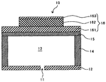
図1において、液滴吐出部10は、インクなどの液体の液滴を吐出するノズル11を有するノズル基板12と、ノズル11に連通し液体を収容した液室13が形成された液室基板14とを備えている。更に、液室基板14(以下、単に「基板」という。)上には、振動板15と、振動板15を介して液室13内の液体を加圧するための電気機械変換素子としての圧電素子16とが設けられている。圧電素子16は、基板14側となる下部電極である共通電極161と、電気機械変換膜として、後述するPZTなどからなる圧電膜162と、圧電膜162の基板14側とは反対側の上部電極である個別電極163とが積層されている。共通電極161は、後述の外部接続用の下部用端子電極である共通電極パッドに接続されている。また、個別電極163は、後述の外部接続用の上部用端子電極である個別電極パッドに接続されている。図1の液滴吐出部10において、共通電極パッド及び個別電極パッドを介して圧電素子16の共通電極161と個別電極163との間に所定の周波数及び振幅の駆動電圧が印加される。この駆動電圧が印加された圧電素子16が、基板14と圧電素子16との間にある図示しない振動板を変形させるように振動し、その振動板の変形により液室13内の液体が加圧され、ノズル11から液滴を吐出させることができる。
DESCRIPTION OF EMBODIMENTS Hereinafter, embodiments for carrying out the present invention will be described with reference to the drawings.
First, the basic configuration of the droplet discharge head according to the present embodiment will be described.
FIG. 1 is a schematic configuration diagram illustrating a configuration example of a
In FIG. 1, a
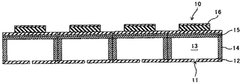
なお、図1では、1つのノズル11からなる液滴吐出部10について説明したが、実際の液滴吐出ヘッドでは、図2に示すように、上記構成の液滴吐出部10を複数個並べて液滴吐出部列を形成している。
In FIG. 1, the liquid
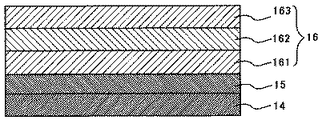
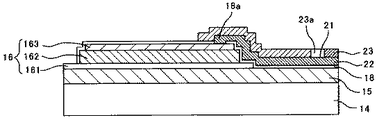
図3は、基板上の振動板及び圧電素子の層構造の一例を示す断面図である。図4及び図5はそれぞれ、圧電素子16周辺のより詳細な断面図及び平面図である。なお、図5において、第1の絶縁保護膜18及び第2の絶縁保護膜23の図示は省略している。
圧電素子16の共通電極161と基板14との間には、成膜により形成された振動板15が配置されている。この振動板15に接するように、圧電素子16を構成する、共通電極161、圧電膜162、個別電極163が積層される。個別電極163が形成された後、圧電膜162、個別電極163はエッチングにより個別化されている。圧電素子16が形成された後、第1の絶縁保護膜18が形成される。更に、共通電極161と下部用端子電極である共通電極パッド19とを接続する共通電極引き出し配線20と、個別電極163と上部用端子電極である個別電極パッド21とを接続する個別電極引き出し配線22と、が形成される。第1の絶縁保護膜18は、共通電極161と個別電極引き出し配線22との間を電気的に絶縁している。また、共通電極161と共通電極引き出し配線20との間、及び、個別電極163と個別電極引き出し配線22との間は、第1の絶縁保護膜18に形成された開口部であるコンタクトホール18aを介して接続されている。
FIG. 3 is a cross-sectional view showing an example of the layer structure of the diaphragm and the piezoelectric element on the substrate. 4 and 5 are a more detailed cross-sectional view and plan view around the
A
上記共通電極引き出し配線20及び個別電極引き出し配線22が形成された後、全体を覆うように第2の絶縁保護膜23が形成される。また、第2の絶縁保護膜23には複数の開口部23aが設けられ、共通電極パッド19、及び、個別電極パッド21が露出している。また、図4に示すように、圧電素子16上に開口部をもつようにしてもよい。この第2の絶縁保護膜23が形成された後の基板14と圧電素子16と各種電極とを含む複合積層基板は、後述するように圧電膜162の極処理がおこなわれて液滴吐出ヘッドを構成するアクチュエータ基板として用いる。すなわち、この複合積層基板は、アクチュエータ基板を作成するための基板であって分極処理がなされる前の分極処理前基板であり、以下「分極前のアクチュエータ基板25」という。
After the common electrode lead-
なお、液滴吐出ヘッドを構成する、アクチュエータ基板を支持するフレーム部材、液体供給手段、流路、流体抵抗等については記載を省略したが、液滴吐出ヘッドに設けることのできる付帯設備を当然に設けることができる。 Note that the description of the frame member that supports the actuator substrate, the liquid supply means, the flow path, the fluid resistance, etc. constituting the droplet discharge head has been omitted, but of course the incidental equipment that can be provided in the droplet discharge head Can be provided.
次に、分極前のアクチュエータ基板25に形成された圧電素子16を構成する圧電膜162の分極処理について説明する
本実施形態では、共通電極パッド19及び個別電極パッド21に対して、コロナ放電方式又はグロー放電方式の放電処理を行っている。この放電処理により、共通電極パッド19及び個別電極パッド21を介して、圧電素子16の共通電極161及び個別電極163に、所定極性の互いに異なる電荷量の電荷を付与している。この電荷付与により、圧電素子16の共通電極161及び個別電極163に挟まれた圧電膜162に対して分極処理を行うことができる。
Next, the polarization process of the
図6は、放電処理による共通電極パッド19及び個別電極パッド21への電荷注入の様子を模式的に示す説明図である。
図6において、ワイヤー状のコロナ電極31を用いて例えばコロナ放電させると、大気中の分子がイオン化して陽イオンと陰イオンが発生する。この発生したイオンのうち、陽イオンが共通電極パッド19及び個別電極パッド21を介して、圧電素子16の共通電極161及び個別電極163に流れ込み、それらの電極に蓄積される。この個別電極163及び共通電極161それぞれに発生する電荷量の差によって、電極間に内部電位差が生じ、圧電膜162の分極処理が行われていると考えられる。
FIG. 6 is an explanatory view schematically showing the state of charge injection into the
In FIG. 6, for example, when corona discharge is performed using a wire-shaped
ここで、圧電膜162の分極処理の状態については、圧電素子のP−Eヒステリシスループ特性から判断することができる。
図7(a)及び(b)はそれぞれ、分極処理前及び分極処理後の圧電素子のP−Eヒステリシスループ特性の測定例を示すグラフである。図7に示すように±150[kV/cm]の電界強度かけてヒステリシスループを測定する。そして、最初の0[kV/cm]時の分極をPiniとし、+150[kV/cm]の電圧印加後、0[kV/cm]まで戻したときの0[kV/cm]時の分極をPrとしたときに、Pr−Piniの値を分極量差として定義する。この分極量差(Pr−Pini)から分極状態の良し悪しを判断することができる。例えば、分極量差(Pr−Pini)は10[μC/cm2]以下となっていることが好ましく、図7(b)に示すように5[μC/cm2]以下となっていることがさらに好ましい。一方、分極量差(Pr−Pini)の値が、図7(a)に示すように10[μC/cm2]よりも大きい場合は、圧電素子からなる圧電アクチュエータとして連続駆動後の変位劣化については、十分な特性が得られない。
Here, the state of the polarization treatment of the
FIGS. 7A and 7B are graphs showing measurement examples of the PE hysteresis loop characteristics of the piezoelectric elements before and after the polarization treatment, respectively. As shown in FIG. 7, the hysteresis loop is measured with an electric field strength of ± 150 [kV / cm]. The first polarization at 0 [kV / cm] is Pini, and after applying a voltage of +150 [kV / cm], the polarization at 0 [kV / cm] when returning to 0 [kV / cm] is Pr. Then, the value of Pr−Pini is defined as a polarization amount difference. Whether the polarization state is good or bad can be determined from this polarization amount difference (Pr-Pini). For example, the polarization amount difference (Pr−Pini) is preferably 10 [μC / cm 2 ] or less, and as shown in FIG. 7B, it is 5 [μC / cm 2 ] or less. Further preferred. On the other hand, when the value of the polarization difference (Pr−Pini) is larger than 10 [μC / cm 2 ] as shown in FIG. 7A, the displacement deterioration after continuous driving as a piezoelectric actuator composed of a piezoelectric element. However, sufficient characteristics cannot be obtained.
分極前のアクチュエータ基板25に分極処理をおこなう分極処理装置としては、以下の構成を用いることができる。本実施形態の分極処理装置は、コロナ電極とグリッド電極、およびサンプルを固定するサンプルステージを具備している。コロナ電極、グリッド電極はそれぞれコロナ電極用電源、グリッド電極用電源に接続されている。サンプルステージは、ステージ上に配置されたサンプルに対して電荷が流れやすくするようにアース接地されていることが好ましい。コロナ電極やグリッド電極に印加する電圧の大きさや、サンプルステージと各電極間の距離は特に限定されるものではなく、十分に分極処理を施すことができるようにこれらを調整し、コロナ放電の強弱をつけることができる。コロナ電極の構成は特に限定されるものではないが、例えば、ワイヤー状のコロナ電極を用いることができ、各種導電性の材料により構成することができる。
As a polarization processing apparatus that performs polarization processing on the
また、グリッド電極は、コロナ電極とサンプルステージとの間に配置されている。グリッド電極の構成は特に限定されるものではないが、形状の工夫や、メッシュ加工を施し、コロナ電極に高電圧を印加したときに、コロナ放電により発生するイオンや電荷等を効率よく均一に下のサンプルステージに降り注ぐように構成されていることが好ましい。 The grid electrode is disposed between the corona electrode and the sample stage. The configuration of the grid electrode is not particularly limited. However, when a high voltage is applied to the corona electrode by applying a shape modification or mesh processing, ions and charges generated by the corona discharge are efficiently and uniformly reduced. It is preferable to be configured to pour onto the sample stage.
サンプルステージには、サンプルを加熱できるように加熱機構が付加されている。これは、加熱しながら分極処理を行った場合、サンプルの応力を緩和させながら処理できるため、所望の分極状態にするために多くの電荷量を供給してもクラックを発生させないためである。電気機械変換素子を加熱する加熱機構の具体的手段は特に限定されるものではなく、各種ヒータやランプ等を用いて加熱するように構成することができる。また、加熱機構は、サンプルステージ内に設置することもでき、サンプルステージ外から加熱するように設置することもできる。特に電極等との干渉を避けるため、サンプルステージ内に設置されていることが好ましい。 A heating mechanism is added to the sample stage so that the sample can be heated. This is because when the polarization process is performed while heating, the sample can be processed while relaxing the stress of the sample, so that a crack is not generated even if a large amount of charge is supplied to obtain a desired polarization state. The specific means of the heating mechanism for heating the electromechanical transducer is not particularly limited, and can be configured to heat using various heaters, lamps and the like. In addition, the heating mechanism can be installed in the sample stage or can be installed so as to heat from outside the sample stage. In particular, in order to avoid interference with an electrode or the like, it is preferable to be installed in the sample stage.
加熱機構の最大加熱温度は特に限定されるものではなく、製造するサンプル、例えば圧電素子の電気機械変換膜のキュリー温度等に応じて所定の温度に加熱できるように構成されていれば良い。特に各種電気機械変換素子に対応できるよう、最大350℃まで加熱できるように構成されていることが好ましい。実際に分極処理を行う際の加熱温度は特に限定されるものではないが、キュリー温度以下に加熱することが好ましい。これは、キュリー温度を超える温度に加熱すると分極処理を行っても再度脱分極してしまい、分極処理の効果がなくなってしまうためである。また、電気機械変換膜の温度がキュリー温度を越えることをより確実に防止するため、加熱温度は特にキュリー温度の半分の温度以下に加熱することが好ましく、1/3以下の温度に加熱することがより好ましい。例えば、電気機械変換膜としてPZTを用いた場合、180℃以下に加熱することが好ましく、120℃以下に加熱することがより好ましい。 The maximum heating temperature of the heating mechanism is not particularly limited as long as the heating mechanism can be heated to a predetermined temperature according to the sample to be manufactured, for example, the Curie temperature of the electromechanical conversion film of the piezoelectric element. In particular, it is preferably configured to be able to heat up to a maximum of 350 ° C. so as to be compatible with various electromechanical conversion elements. Although the heating temperature at the time of actually performing a polarization process is not specifically limited, It is preferable to heat below Curie temperature. This is because if the heating is performed at a temperature exceeding the Curie temperature, depolarization occurs again even if the polarization treatment is performed, and the effect of the polarization treatment is lost. In order to more reliably prevent the temperature of the electromechanical conversion film from exceeding the Curie temperature, the heating temperature is preferably heated to a temperature equal to or lower than half of the Curie temperature, and preferably heated to a temperature equal to or lower than 1/3. Is more preferable. For example, when PZT is used as the electromechanical conversion film, it is preferably heated to 180 ° C. or lower, more preferably 120 ° C. or lower.
また、サンプルステージには、コロナ放電した時にサンプルに電荷等が照射(供給)されるエリアが限られるため、サンプル全体を処理できるようにサンプルの移動が可能な移動機構が付加されている。移動手段は特に限定するものではない。 In addition, since the area where the sample is irradiated (supplied) with charges or the like when corona discharge is applied to the sample stage, a moving mechanism capable of moving the sample is added so that the entire sample can be processed. The moving means is not particularly limited.
また、分極処理を行う際に必要な電荷量Qについては特に限定されるものではないが、電気機械変換素子に1.0×10⁻⁸[C]以上の電荷量が蓄積されることが好ましく、4.0×10⁻⁸[C]以上の電荷量が蓄積されることがさらに好ましい。係る範囲の電荷量を電気機械変換素子に蓄積させることにより、より確実に上記分極量差を有するように良好な分極処理を行うことができる。 In addition, the amount of charge Q required for performing the polarization treatment is not particularly limited, but it is preferable that a charge amount of 1.0 × 10 −8 [C] or more is accumulated in the electromechanical transducer. More preferably, a charge amount of 4.0 × 10 −8 [C] or more is accumulated. By accumulating the charge amount in such a range in the electromechanical conversion element, it is possible to perform a favorable polarization process so as to have the above polarization amount difference more reliably.
ここで、従来の構成における問題点について説明する。従来の構成では、分極前のアクチュエータ基板25の個別電極パッド21はすべて同じ大きさである。一方、圧電膜162の分極処理に用いられるコロナ電極のコロナ放電では、コロナ電極の直下では放電が強く、コロナ電極の直下から離れるに従って放電が弱くなる。このため、複数の個別電極パッド21のうち、コロナ電極から水平方向に近い位置に配置されている個別電極パッド21には所定量の電荷を供給できる。しかし、コロナ電極から水平方向に遠い位置に配置されている個別電極パッド21に供給される電荷量が減少し、個別電極パッド21を介して圧電素子16の個別電極163に流れ込み蓄積される電荷量が減少する。このため、コロナ電極から水平方向に遠い位置に配置されている圧電素子16では分極処理が不十分になる。図8は、個別電極パッドのコロナ電極の配置位置からの水平距離による分極量差(Pr−Pini)の分布を示すグラフである。コロナ電極の直下から遠くなるに伴い、圧電素子16の分極量差(Pr−Pini)は大きくなり、分極処理が不十分になっていることが認められる。
Here, problems in the conventional configuration will be described. In the conventional configuration, the
このように、コロナ放電を用いた分極処理では良好な分極処理がおこなわれる範囲が限られてしまい、分極前のアクチュエータ基板25の一括分極処理が困難となる。このため、コロナ電極の近くに個別電極パッド21が配置されるよう、分極前のアクチュエータ基板25を移動させて分極処理を行う必要があり、時間を要してしまう。
Thus, in the polarization process using corona discharge, the range in which a good polarization process is performed is limited, and the collective polarization process of the
また、分極処理によるクラックの発生を抑制するために、分極前のアクチュエータ基板25を上記加熱装置により加熱しながら分極処理を行うことが有利である。しかしながら、コロナ放電による分極処理可能な範囲が限られることで、分極処理可能な範囲外では加熱により脱分極が生じてしまい、これにより分極処理の効果が低下してしまう。
Further, in order to suppress the generation of cracks due to the polarization treatment, it is advantageous to perform the polarization treatment while heating the
そこで、本実施形態の分極前のアクチュエータ基板25では、コロナ電極から水平方向に関して遠い位置において、コロナ電極から水平方向に関して近い位置よりも、個別電極パッド21の表面積を大きくする。これにより、コロナ電極から水平方向に関して遠い位置の個別電極パッド21に供給される電荷量と、近い位置の個別電極パッド21に供給される電荷量を均一化している。その結果、コロナ電極から遠い位置にある圧電素子16に対しても、コロナ電極から近い位置にある圧電素子16と同様に、良好な分極処理が可能となる。
Therefore, in the
以下に、本実施形態のアクチュエータ基板25を構成する材料、工法について具体的に説明する。
Below, the material and construction method which comprise the actuator board |
〔基板〕
基板14としては、シリコン単結晶基板を用いることが好ましく、通常100[μm]以上600[μm]以下の範囲の厚みを持つことが好ましい。面方位としては、(100)、(110)、(111)と3種あるが、半導体産業では一般的に(100)、(111)が広く使用されており、本構成例においては、主に(100)の面方位を持つ単結晶基板を主に使用した。また、図1に示すような液室(圧力室)13を作製していく場合、エッチングを利用してシリコン単結晶基板を加工していく。この場合のエッチング方法としては、異方性エッチングを用いることが一般的である。異方性エッチングとは結晶構造の面方位に対してエッチング速度が異なる性質を利用したものである。例えばKOH等のアルカリ溶液に浸漬させた異方性エッチングでは、(100)面に比べて(111)面は約1/400程度のエッチング速度となる。従って、面方位(100)では約54°の傾斜を持つ構造体が作製できるのに対して、面方位(110)では深い溝をほることができるため、より剛性を保ちつつ、配列密度を高くすることができることが分かっている。本構成例としては(110)の面方位を持った単結晶基板を使用することも可能である。但し、この場合、マスク材であるSiO2もエッチングされてしまうため、この点も留意して利用することが好ましい。
〔substrate〕
As the
〔振動板〕
図1に示すように電気機械変換素子としての圧電素子16によって発生した力を受けて、その下地の振動板15が変形して、液室(圧力室)13のインクなどの液体の液滴を吐出させる。そのため、振動板15としては所定の強度を有したものであることが好ましい。材料としては、Si、SiO2、Si3N4などを例えばCVD(Chemical Vapor Deposition)法により作製したものが挙げられる。さらに図1に示すような共通電極161及び圧電膜162の線膨張係数に近い材料を選択することが好ましい。特に、圧電膜としては、一般的に材料として、後述するPZTが使用される場合が多い。従って、振動板15の材料は、PZTの線膨張係数8×10⁻⁶(1/K)に近い5×10−6(1/K)以上10×10−6(1/K)以下の範囲の線膨張係数を有した材料が好ましく、さらには7×10−6(1/K)以上9×10−6(1/K)以下の範囲の線膨張係数を有した材料がより好ましい。具体的な材料としては、酸化アルミニウム、酸化ジルコニウム、酸化イリジウム、酸化ルテニウム、酸化タンタル、酸化ハフニウム、酸化オスミウム、酸化レニウム、酸化ロジウム、酸化パラジウム及びそれらの化合物等が挙げられる。これらの材料を、例えばスパッタ法又はゾルゲル法を用いてスピンコーターにて作製することができる。膜厚としては0.1[μm]以上10[μm]以下の範囲が好ましく、0.5[μm]以上3[μm]以下の範囲がさらに好ましい。この範囲より小さいと、図1に示すような液室(圧力室)13の加工が難しくなる。また、上記範囲より大きいと振動板15が変形しにくくなり、インク滴などの液滴の吐出が不安定になる。
(Diaphragm)
As shown in FIG. 1, upon receiving the force generated by the
[共通電極(下部電極)]
共通電極(下部電極)161としては、金属もしくは金属と酸化物からなっていることが好ましい。ここで、どちらの材料も振動板15と共通電極161を構成する金属膜との間に密着層を入れて剥がれ等を抑制するように工夫している。以下に密着層含めて金属電極膜及び酸化物電極膜の詳細について記載する。
[Common electrode (lower electrode)]
The common electrode (lower electrode) 161 is preferably made of metal or a metal and an oxide. Here, both materials are devised so as to suppress peeling and the like by inserting an adhesion layer between the
[密着層]
密着層は、例えば次のように形成する。Tiをスパッタ成膜後、成膜したチタン膜をRTA(Rapid Thermal Annealing)装置を用いて熱酸化して酸化チタン膜にする。熱酸化の条件は、例えば、650[℃]以上800[℃]以下の範囲の温度、1[分]以上30[分]以下の範囲の処理時間、及びO2雰囲気である。酸化チタン膜を作成するには反応性スパッタでもよいがチタン膜の高温による熱酸化法が望ましい。反応性スパッタによる作製では、シリコン基板を高温で加熱する必要があるため、特別なスパッタチャンバ構成を必要とする。さらに、一般の炉による酸化よりも、RTA装置による酸化の方がチタンO2膜の結晶性が良好になる。なぜなら、通常の加熱炉による酸化によれば、酸化しやすいチタン膜は、低温においてはいくつもの結晶構造を作るため、一旦、それを壊す必要が生じるためである。したがって、昇温速度の速いRTAによる酸化の方が良好な結晶を形成するために有利になる。また、Ti以外の材料としては、Ta、Ir、Ru等の材料を用いることもできる。密着層の膜厚としては、10[nm]以上50[nm」以下の範囲が好ましく、15[nm]以上30[nm]以下の範囲がさらに好ましい。この範囲以下の場合においては、密着性に懸念があり、また、この範囲以上になってくると、その密着層の上で作製する電極膜の結晶の質に影響が出てくる。
[Adhesion layer]
The adhesion layer is formed as follows, for example. After Ti is formed by sputtering, the formed titanium film is thermally oxidized using an RTA (Rapid Thermal Annealing) apparatus to form a titanium oxide film. The conditions for thermal oxidation are, for example, a temperature in the range of 650 [° C.] to 800 [° C.], a treatment time in the range of 1 [min] to 30 [min], and an O 2 atmosphere. To form the titanium oxide film, reactive sputtering may be used, but thermal oxidation of the titanium film at a high temperature is desirable. The production by reactive sputtering requires a special sputtering chamber configuration because the silicon substrate needs to be heated at a high temperature. Furthermore, the crystallinity of the titanium O 2 film is better in the oxidation by the RTA apparatus than in the oxidation by a general furnace. This is because, according to oxidation in a normal heating furnace, a titanium film that is easily oxidized forms several crystal structures at a low temperature, and thus it is necessary to break it once. Therefore, oxidation by RTA having a high temperature rising rate is advantageous in order to form better crystals. Moreover, as materials other than Ti, materials such as Ta, Ir, and Ru can be used. The thickness of the adhesion layer is preferably in the range of 10 [nm] to 50 [nm], and more preferably in the range of 15 [nm] to 30 [nm]. If it is below this range, there is concern about the adhesion, and if it exceeds this range, the quality of the crystal of the electrode film produced on the adhesion layer will be affected.
〔金属電極膜〕
金属電極膜の金属材料としては、従来から高い耐熱性と低い反応性を有する白金が用いられているが、鉛に対しては十分なバリア性を持つとはいえない場合もあり、イリジウムや白金−ロジウムなどの白金族元素や、これらの合金膜も挙げられる。また、白金を使用する場合には下地(特にSiO2)との密着性が悪いために、前述の密着層を先に積層することが好ましい。作製方法としては、スパッタ法や真空蒸着等の真空成膜が一般的である。膜厚としては、80[nm]以上200[nm]以下の範囲が好ましく、100[nm]以上150[nm]以下の範囲がより好ましい。この範囲より薄い場合においては、共通電極161として十分な電流を供給することができなくなり、液滴の吐出をする際に不具合が発生する。さらに、この範囲より厚い場合においては、白金族元素の高価な材料を使用する場合においては、コストアップとなる。また、白金を材料とした場合においては、膜厚を厚くしていたったときに表面粗さが大きくなり、その上に作製する酸化物電極膜やPZTの表面粗さや結晶配向性に影響を及ぼして、インク吐出に十分な変位が得られないような不具合が発生する。
[Metal electrode film]
Conventionally, platinum having high heat resistance and low reactivity has been used as the metal material of the metal electrode film, but it may not be said that it has sufficient barrier properties against lead. -Platinum group elements, such as rhodium, and these alloy films are also mentioned. Further, when platinum is used, it is preferable that the above-mentioned adhesion layer is laminated first because adhesion to the base (particularly SiO 2 ) is poor. As a manufacturing method, vacuum film formation such as sputtering or vacuum deposition is generally used. The film thickness is preferably in the range of 80 [nm] to 200 [nm], and more preferably in the range of 100 [nm] to 150 [nm]. When the thickness is smaller than this range, a sufficient current cannot be supplied as the
〔酸化物電極膜〕
酸化物電極膜の材料としては、ルテニウム酸ストロンチウム(SrRuO3、以下適宜「SRO」と略す。)を用いることが好ましい。ルテニウム酸ストロンチウムの一部を置換した材料、具体的には、SrxA(1−x)RuyB(1−y)O3(式中、AはBa、Ca、 BはCo、Ni、 x、y=0〜0.5)で表される材料についても好ましく用いることができる。酸化物電極膜は、例えばスパッタ法等の成膜方法により作製することができる。スパッタ条件によってSrRuO3の薄膜の膜質が変わる。従って、特に結晶配向性を重視し、共通電極のPt(111)にならってSrRuO3の膜についても(111)配向させるためには、成膜温度については500[℃]以上での基板加熱を行い、成膜することが好ましい。例えば特許文献2に記載のSRO成膜条件については、室温成膜でその後、RTA処理にて結晶化温度(650℃)で熱酸加している。この場合、SRO膜としては、十分結晶化され、電極としての比抵抗としても十分な値が得られるが、膜の結晶配向性としては、(110)が優先配向しやすくなり、その上に成膜したPZTについても(110)配向しやすくなる。
[Oxide electrode film]
As a material for the oxide electrode film, strontium ruthenate (SrRuO 3 , hereinafter, abbreviated as “SRO” as appropriate) is preferably used. A material in which a part of strontium ruthenate is substituted, specifically, Sr x A (1-x) Ru y B (1-y) O 3 (where A is Ba, Ca, B is Co, Ni, The material represented by x, y = 0 to 0.5) can also be preferably used. The oxide electrode film can be produced by a film forming method such as sputtering. The film quality of the SrRuO 3 thin film varies depending on the sputtering conditions. Accordingly, in order to place the SrRuO 3 film in the (111) orientation in accordance with the common electrode Pt (111) with particular emphasis on the crystal orientation, it is necessary to heat the substrate at a deposition temperature of 500 [° C.] or higher. Preferably, the film is formed. For example, with respect to the SRO film formation conditions described in Patent Document 2, thermal oxidation is performed at room temperature film formation and then at a crystallization temperature (650 ° C.) by RTA treatment. In this case, the SRO film is sufficiently crystallized and a sufficient value is obtained as the specific resistance as an electrode. However, as the crystal orientation of the film, (110) is easily preferentially oriented, and the film is formed thereon. The (110) orientation of the deposited PZT is also facilitated.
Pt(111)上に作製したSROの結晶性については、PtとSROで格子定数が近いため、通常のX線のθ−2θ測定では、SRO(111)とPt(111)の2θ位置が重なってしまい判別が難しい。Ptについては消滅則の関係からPsi=35°だけ傾けた2θが約32°付近の位置には回折線が打ち消し合い、回折強度が見られない。そのため、Psi方向を約35°傾けて、2θが約32°付近のピーク強度で判断することで、SROが(111)に優先配向しているかを確認することができる。 As for the crystallinity of SRO produced on Pt (111), the lattice constants of Pt and SRO are close to each other. Therefore, in the normal X-ray θ-2θ measurement, the 2θ positions of SRO (111) and Pt (111) overlap. It is difficult to distinguish. With respect to Pt, diffraction lines cancel each other at a position where 2θ inclined by Psi = 35 ° is about 32 ° due to the disappearance rule, and no diffraction intensity is observed. Therefore, it is possible to confirm whether the SRO is preferentially oriented to (111) by inclining the Psi direction by about 35 ° and judging from the peak intensity where 2θ is about 32 °.
図9に、2θ=32°に固定し、Psiを振ったときのデータを示す。Psi=0°ではSRO(110)ではほとんど回折強度が見られず、Psi=35°付近において、回折強度が見られる。これより、本成膜条件にて作製したものについては、SROが(111)配向していることが確認できた。また、上述記載の室温成膜+RTA処理により作製されたSROについては、Psi=0°のときにSRO(110)の回折強度が見られる。 FIG. 9 shows data when 2θ = 32 ° is fixed and Psi is shaken. At Psi = 0 °, almost no diffraction intensity is observed at SRO (110), and diffraction intensity is observed at around Psi = 35 °. From this, it was confirmed that the SRO was (111) oriented for those fabricated under the present film forming conditions. In addition, regarding the SRO produced by the room temperature film formation + RTA process described above, the diffraction intensity of SRO (110) is observed when Psi = 0 °.
また、圧電アクチュエータとして連続動作したときに、駆動させた後の変位量が、初期変位に比べてどのくらい劣化したかを見積もったところ、PZTの配向性が非常に影響しており、(110)では変位劣化抑制において不十分である。さらにSRO膜の表面粗さを見たときに、成膜温度に影響し、室温から300℃では表面粗さが非常に小さく2[nm]以下になる。粗さについてはAFMにより測定される表面粗さ(平均粗さ)を指標としている。表面粗さとしては、非常にフラットにはなっているが結晶性が十分でなく、その後成膜した圧電膜(PZT膜)の圧電アクチュエータとしての初期変位や連続駆動後の変位劣化については十分な特性が得られない。表面粗さとしては、4[nm]以上15[nm]の範囲になっていることが好ましく、6[nm]以上10[nm]以下の範囲がさらに好ましい。この範囲を超えると、その後成膜したPZTの絶縁耐圧が非常に悪く、リークしやすくなる。従って上述に示すような、結晶性や表面粗さを得るためには、成膜温度としては500[℃]以上700[℃]、好ましくは520[℃]以上600[℃]の範囲で成膜を実施している。 In addition, when the amount of displacement after being driven was estimated to be deteriorated compared to the initial displacement when continuously operating as a piezoelectric actuator, the orientation of PZT has a great influence. (110) Insufficient displacement suppression is insufficient. Further, when the surface roughness of the SRO film is observed, it affects the film forming temperature, and the surface roughness is very small from room temperature to 300 ° C. and becomes 2 [nm] or less. As for the roughness, the surface roughness (average roughness) measured by AFM is used as an index. Although the surface roughness is very flat, the crystallinity is not sufficient, and the initial displacement as the piezoelectric actuator of the piezoelectric film (PZT film) formed thereafter and the displacement deterioration after continuous driving are sufficient. Characteristics are not obtained. The surface roughness is preferably in the range of 4 [nm] to 15 [nm], and more preferably in the range of 6 [nm] to 10 [nm]. If this range is exceeded, the dielectric breakdown voltage of the PZT deposited thereafter is very poor and leaks easily. Therefore, in order to obtain crystallinity and surface roughness as described above, the film formation temperature is 500 [° C.] to 700 [° C.], preferably 520 [° C.] to 600 [° C.]. Has been implemented.
成膜後のSrとRuの組成比については、Sr/Ruが0.82以上1.22以下であることが好ましい。この範囲から外れると比抵抗が大きくなり、電極として十分な導電性が得られなくなる。更に、SRO膜の膜厚としては、40[nm]以上150[nm]以下の範囲が好ましく、50[nm]以上80[nm]以下の範囲がさらに好ましい。この膜厚範囲よりも薄いと初期変位や連続駆動後の変位劣化については十分な特性が得られず、圧電膜(PZT膜)のオーバーエッチングを抑制するためのストップエッチング層としての機能も得られにくくなる。また、この膜厚範囲を超えると、その後に成膜した圧電膜(PZT膜)の絶縁耐圧が非常に悪く、リークしやすくなる。また、比抵抗としては、5×10−3[Ω・cm]以下になっていることが好ましく、さらに1×10−3[Ω・cm]以下になっていることがさらに好ましい。この範囲よりも大きくなると共通電極161として、共通電極引き出し配線20との界面で接触抵抗が十分得られず、共通電極161として十分な電流を供給することが出来なくなり、液滴を吐出する際に不具合が発生する。
Regarding the composition ratio of Sr and Ru after film formation, Sr / Ru is preferably 0.82 or more and 1.22 or less. If it is out of this range, the specific resistance increases, and sufficient conductivity as an electrode cannot be obtained. Furthermore, the thickness of the SRO film is preferably in the range of 40 [nm] to 150 [nm], and more preferably in the range of 50 [nm] to 80 [nm]. If the thickness is smaller than this range, sufficient characteristics cannot be obtained for initial displacement and displacement deterioration after continuous driving, and a function as a stop etching layer for suppressing over-etching of the piezoelectric film (PZT film) can also be obtained. It becomes difficult. If the thickness is exceeded, the dielectric strength of the piezoelectric film (PZT film) formed thereafter is very poor and leaks easily. Further, the specific resistance is preferably 5 × 10 −3 [Ω · cm] or less, and more preferably 1 × 10 −3 [Ω · cm] or less. If it is larger than this range, sufficient contact resistance cannot be obtained at the interface with the common electrode lead-
〔圧電膜(電気機械変換膜)〕
圧電膜162の材料としては、PZTを主に使用した。PZTとはジルコン酸鉛(PbTiO3)とチタン酸(PbTiO3)の固溶体で、その比率により特性が異なる。一般的に優れた圧電特性を示す組成はPbZrO3とPbTiO3の比率が53:47の割合で、化学式で示すとPb(Zr0.53,Ti0.47)O3、一般PZT(53/47)と示される。PZT以外の複合酸化物としてはチタン酸バリウムなどが挙げられ、この場合はバリウムアルコキシド、チタンアルコキシド化合物を出発材料にし、共通溶媒に溶解させることでチタン酸バリウム前駆体溶液を作製することも可能である。これら材料は一般式ABO3で記述され、A=Pb、Ba、Sr、 B=Ti、Zr、Sn、Ni、Zn、Mg、Nbを主成分とする複合酸化物が該当する。その具体的な記述として(Pb1−x,Bax)(Zr,Ti)O3、(Pb1−x,Srx)(Zr,Ti)O3、これはAサイトのPbを一部BaやSrで置換した場合である。このような置換は2価の元素であれば可能であり、その効果は熱処理中の鉛の蒸発による特性劣化を低減させる作用を示す。
[Piezoelectric film (electromechanical conversion film)]
PZT was mainly used as the material for the
圧電膜162の作製方法としては、スパッタ法もしくは、ゾルゲル法を用いてスピンコーターにて作製することができる。その場合は、パターニング化が必要となるので、フォトリソエッチング等により所望のパターンを得る。PZTをゾルゲル法により作製した場合、出発材料に酢酸鉛、ジルコニウムアルコキシド、チタンアルコキシド化合物を出発材料にし、共通溶媒としてメトキシエタノールに溶解させ均一溶液を得ることで、PZT前駆体溶液が作製できる。金属アルコキシド化合物は大気中の水分により容易に加水分解してしまうので、前駆体溶液に安定剤としてアセチルアセトン、酢酸、ジエタノールアミンなどの安定化剤を適量、添加してもよい。
As a method for manufacturing the
基板14の全面に圧電膜(PZT膜)162を得る場合、スピンコートなどの溶液塗布法により塗膜を形成し、溶媒乾燥、熱分解、結晶化の各々の熱処理を施すことで得られる。塗膜から結晶化膜への変態には体積収縮が伴うので、クラックフリーな膜を得るには一度の工程で100[nm]以下の膜厚が得られるように前駆体濃度の調整が必要になる。
When the piezoelectric film (PZT film) 162 is obtained on the entire surface of the
圧電膜162の膜厚としては0.5[μm]以上5[μm]以下の範囲が好ましく、1[μm]以上2[μm]以下の範囲がより好ましい。この範囲より小さいと十分な変形(変位)を発生することができなくなり、この範囲より大きいと何層も積層させていくため、工程数が多くなりプロセス時間が長くなる。
また、圧電膜162の比誘電率としては600以上2000以下の範囲になっていることが好ましく、さらに1200以上1600以下の範囲になっていることが好ましい。このとき、この範囲よりも小さいときには十分な変形(変位)特性が得られないといった不具合が発生する。一方、この範囲より大きくなると、分極処理が十分行われず、連続駆動後の変位劣化については十分な特性が得られないといった不具合が発生する。
The film thickness of the
The relative dielectric constant of the
〔個別電極(上部電極)〕
個別電極(上部電極)163としては、金属もしくは酸化物と金属からなっていることが好ましい。以下に酸化物電極膜及び金属電極膜の詳細について記載する。
[Individual electrode (upper electrode)]
The individual electrode (upper electrode) 163 is preferably made of a metal or an oxide and a metal. Details of the oxide electrode film and the metal electrode film are described below.
〔酸化物電極膜〕
酸化物電極膜の材料等については、前述の共通電極(下部電極)161で使用した酸化物電極膜について記載したものと同様なものを挙げることができる。酸化物電極膜(SRO膜)の膜厚としては、20[nm]以上80[nm]以下の範囲が好ましく、40[nm]以上60[nm]以下の範囲がさらに好ましい。この膜厚範囲よりも薄いと初期変形(変位)や変形(変位)の劣化特性については十分な特性が得られない。また、この範囲を超えると、その後に成膜した圧電膜(PZT膜)162の絶縁耐圧が非常に悪く、リークしやすくなる。
[Oxide electrode film]
As for the material and the like of the oxide electrode film, the same materials as those described for the oxide electrode film used in the common electrode (lower electrode) 161 can be given. The thickness of the oxide electrode film (SRO film) is preferably in the range of 20 [nm] to 80 [nm], and more preferably in the range of 40 [nm] to 60 [nm]. If the thickness is less than this range, sufficient characteristics cannot be obtained for the deterioration characteristics of initial deformation (displacement) and deformation (displacement). In addition, if this range is exceeded, the dielectric breakdown voltage of the piezoelectric film (PZT film) 162 formed thereafter is very poor and leaks easily.
〔金属電極膜〕
金属電極膜の材料等については、前述の共通電極(下部電極)161で使用した金属電極膜について記載したものと同様なものを挙げることができる。金属電極膜とで記載しており、膜厚としては30[nm]以上200[nm]以下の範囲が好ましく、50[nm]以上120[nm]以下の範囲がさらに好ましい。この範囲より薄い場合においては、個別電極163として十分な電流を供給することができなくなり、液滴を吐出する際に不具合が発生する。また、上記範囲より厚いと、白金族元素の高価な材料を使用する場合にコストアップとなる。また、白金を材料とした場合に膜厚を厚くしていたったときに表面粗さが大きくなり、絶縁保護膜を介して配線などを作製する際に、膜剥がれ等のプロセス不具合が発生しやすくなる。
[Metal electrode film]
Examples of the material for the metal electrode film include the same materials as those described for the metal electrode film used in the common electrode (lower electrode) 161 described above. The film thickness is described as a metal electrode film, and the film thickness is preferably in the range of 30 [nm] to 200 [nm], and more preferably in the range of 50 [nm] to 120 [nm]. When the thickness is smaller than this range, a sufficient current cannot be supplied as the
〔第1の絶縁保護膜〕
成膜・エッチングの工程による圧電素子へのダメージを防ぐとともに、大気中の水分が透過しづらい材料を選定する必要があるため、第1の絶縁保護膜18の材料は緻密な無機材料とする必要がある。また、第1の絶縁保護膜18として有機材料を用いる場合は、十分な保護性能を得るために膜厚を厚くする必要があるため、適さない。第1の絶縁保護膜18を厚い膜とした場合、振動板15の振動を著しく阻害してしまうため、吐出性能の低い液滴吐出ヘッドになってしまう。薄膜で高い保護性能を得るには、酸化物,窒化物,炭化膜を用いるのが好ましいが、第1の絶縁保護膜18の下地となる電極材料、圧電体材料及び振動板材料と密着性が高い材料を選定する必要がある。また、第1の絶縁保護膜18の成膜法も、圧電素子16を損傷しない成膜方法を選定する必要がある。すなわち、反応性ガスをプラズマ化して基板上に堆積するプラズマCVD法やプラズマをターゲット材に衝突させて飛ばすことで成膜するスパッタリング法は好ましくない。第1の絶縁保護膜18の好ましい成膜方法としては、蒸着法、ALD(Atomic Layer Deposition)法などが例示できるが、使用できる材料の選択肢が広いALD法が好ましい。好ましい材料としては、Al2O3,ZrO2,Y2O3,Ta2O3,TiO2などのセラミクス材料に用いられる酸化膜が例として挙げられる。特にALD法を用いることで、膜密度の非常に高い薄膜を作製し、プロセス中でのダメージを抑制することができる。
[First insulating protective film]
Since it is necessary to select a material that prevents the moisture in the atmosphere from permeating while preventing damage to the piezoelectric element due to the film formation / etching process, the material of the first insulating
第1の絶縁保護膜18の膜厚は、圧電素子16の保護性能を確保できる十分な薄膜とする必要があると同時に、振動板15の変形(変位)を阻害しないように可能な限り薄くする必要がある。第1の絶縁保護膜18の膜厚は、20[nm]以上100[nm]以下の範囲が好ましい。100[nm]より厚い場合は、振動板15の変形(変位)量が低下するため、吐出効率の低い液滴吐出ヘッドとなる。一方、20[nm]より薄い場合は、圧電素子16の保護層としての機能が不足してしまうため、圧電素子16の性能が前述の通り低下してしまう。
The film thickness of the first insulating
また、第1の絶縁保護膜18を2層にする構成も考えられる。この場合は、2層目の絶縁保護膜を厚くするため、振動板15の振動を著しく阻害しないように個別電極(上部電極)163付近において2層目の絶縁保護膜を開口するような構成も挙げられる。この場合、2層目の絶縁保護膜としては、任意の酸化物,窒化物,炭化物またはこれらの複合化合物を用いることができ、また、半導体デバイスで一般的に用いられるSiO2を用いることもできる。2層の第1の絶縁保護膜18の成膜は任意の手法を用いることができ、例えばCVD法、スパッタリング法等が例示できる。電極形成部等のパターン形成部の段差被覆を考慮すると等方的に成膜できるCVD法を用いることが好ましい。2層目の絶縁保護膜の膜厚は共通電極(下部電極)161と個別電極引き出し配線22との間に印加される電圧で絶縁破壊されない膜厚とする必要がある。すなわち第1の絶縁保護膜18に印加される電界強度を、絶縁破壊しない範囲に設定する必要がある。さらに、第1の絶縁保護膜18の下地の表面性やピンホール等を考慮すると、第1の絶縁保護膜18の膜厚は200[nm]以上必要であり、さらに好ましくは500[nm]以上である。
Further, a configuration in which the first insulating
〔配線〕
共通電極引き出し配線20、個別電極引き出し配線22の材料は、Ag合金、Cu、Al、Au、Pt、Irのいずれかから成る金属電極材料であることが好ましい。これらの配線の作製方法としては、スパッタ法、スピンコート法を用いて作製し、その後フォトリソエッチング等により所望のパターンを得る。膜厚としては、0.1[μm]以上20[μm]以下の範囲が好ましく、0.2[μm]以上10[μm]以下の範囲がさらに好ましい。この範囲より小さいと抵抗が大きくなり電極に十分な電流を流すことができなくなりヘッド吐出が不安定になる。一方、この範囲より大きいとプロセス時間が長くなる。また、共通電極161及び個別電極163に接続されるコンタクトホール部(例えば10[μm]×10[μm])での接触抵抗としては、共通電極161に対して10[Ω]以下、個別電極163に対して1[Ω]以下が好ましい。さらに好ましくは、共通電極161に対して5[Ω]以下、個別電極163に対して0.5[Ω]以下である。この範囲を超えると十分な電流を供給することができなくなり、液滴を吐出をする際に不具合が発生する。
〔wiring〕
The material of the common electrode lead-
共通電極引き出し配線20のうち、第2の絶縁保護膜23の開口部(不図示)から露出している部分が下部用端子電極としての共通電極パッド19となる。また、個別電極引き出し配線22のうち、第2の絶縁保護膜23の開口部23aから露出している部分が上部用端子電極としての個別電極パッド21となる。このため、共通電極引き出し配線20、個別電極引き出し配線22は、後述する共通電極パッド19および個別電極パッド21の大きさが得られるよう所望の大きさにパターン化する。
Of the common electrode lead-
〔第2の絶縁保護膜〕
第2の絶縁保護膜23としての機能は、個別電極引き出し配線22や共通電極引き出し配線20の保護層としての機能を有するパシベーション層である。第2の絶縁保護膜23は、前述のように、個別電極パッド21を形成するための開口部23aと共通電極パッド19を形成するための開口部(不図示)を除き、個別電極引き出し配線22や共通電極引き出し配線20を被覆する。これにより、電極材料に安価なAlもしくはAlを主成分とする合金材料を用いることができる。その結果、低コストかつ信頼性の高い液滴吐出ヘッド(インクジェットヘッド)とすることができる。第2の絶縁保護膜23の材料としては、任意の無機材料、有機材料を使用することができるが、透湿性の低い材料とする必要がある。無機材料としては、酸化物、窒化物、炭化物等が例示でき、有機材料としてはポリイミド、アクリル樹脂、ウレタン樹脂等が例示できる。ただし、有機材料の場合には厚膜とすることが必要となるため、パターニングに適さない。そのため、薄膜で配線保護機能を発揮できる無機材料とすることが好ましい。特に、Al配線上にSi3N4を用いることが、半導体デバイスで実績のある技術であるため好ましい。また、膜厚は200[nm]以上とすることが好ましく、さらに好ましくは500[nm]以上である。膜厚が薄い場合は十分なパシベーション機能を発揮できないため、配線材料の腐食による断線が発生し、インクジェットの信頼性を低下させてしまう。
[Second insulating protective film]
The function as the second insulating
また、図4に示すように、圧電素子16上とその周囲の振動板15上に開口部をもつ構造が好ましい。これは、前述の第1の絶縁保護膜18の個別液室に対応した領域を薄くしていることと同様の理由である。これにより、高効率かつ高信頼性の液滴吐出ヘッド(インクジェットヘッド)とすることが可能になる。絶縁保護膜18、23で圧電素子16が保護されているため、第2の絶縁保護膜23の開口部の形成には、フォトリソグラフィー法とドライエッチングを用いることができる。また、第2の絶縁保護膜23の開口部により設けられる個別電極パッド21、共通電極パッド19の面積については、実施例にて詳細に説明する。
Also, as shown in FIG. 4, a structure having openings on the
次に、本実施形態のアクチュエータ基板の製造方法における放電を用いた分極処理のより具体的な実施例について説明する。 Next, a more specific example of polarization processing using discharge in the method for manufacturing the actuator substrate of the present embodiment will be described.
<実施例1>
実施例1では、基板14としての6インチシリコンウェハに熱酸化膜(膜厚1[μm])を形成し、共通電極161を形成した。まず、共通電極161の密着膜として、チタン膜(膜厚30[nm])をスパッタ装置にて成膜した後、RTAを用いて750[℃]にて熱酸化した。引き続き、金属膜として白金膜(膜厚100[nm])、酸化物膜としてSrRuO膜(膜厚60[nm])をスパッタ成膜した。スパッタ成膜時の基板加熱温度については550[℃]にて成膜を実施した。
<Example 1>
In Example 1, a thermal oxide film (film thickness: 1 [μm]) was formed on a 6-inch silicon wafer as the
次に、圧電膜(電気機械変換膜)163を形成した。まず、Pb:Zr:Ti=114:53:47に調整された溶液を準備し、スピンコート法により膜を成膜した。具体的な前駆体塗布液の合成については、出発材料に酢酸鉛三水和物、イソプロポキシドチタン、イソプロポキシドジルコニウムを用いた。酢酸鉛の結晶水はメトキシエタノールに溶解後、脱水した。化学両論組成に対し鉛量を過剰にしてある。これは熱処理中のいわゆる鉛抜けによる結晶性低下を防ぐためである。イソプロポキシドチタン、イソプロポキシドジルコニウムをメトキシエタノールに溶解し、アルコール交換反応、エステル化反応を進め、先記の酢酸鉛を溶解したメトキシエタノール溶液と混合することでPZT前駆体溶液を合成した。このPZT前駆体溶液のPZT濃度は0.5モル/リットルした。このPZT前駆体溶液を用いて、スピンコートにより成膜し、その成膜後、120[℃]での乾燥と500[℃]での熱分解とを行った。3層目の熱分解処理後に、結晶化熱処理(温度750[℃])をRTA(急速熱処理)にて行った。このときPZTの膜厚は240[nm]であった。この工程を合計8回(24層)実施し、約2[μm]のPZT膜厚を得た。 Next, a piezoelectric film (electromechanical conversion film) 163 was formed. First, a solution adjusted to Pb: Zr: Ti = 114: 53: 47 was prepared, and a film was formed by spin coating. For the synthesis of a specific precursor coating solution, lead acetate trihydrate, isopropoxide titanium and isopropoxide zirconium were used as starting materials. Crystal water of lead acetate was dissolved in methoxyethanol and then dehydrated. The lead amount is excessive with respect to the stoichiometric composition. This is to prevent crystallinity deterioration due to so-called lead loss during heat treatment. Isopropoxide titanium and isopropoxide zirconium were dissolved in methoxyethanol, the alcohol exchange reaction and the esterification reaction were advanced, and the PZT precursor solution was synthesized by mixing with the methoxyethanol solution in which the lead acetate was dissolved. The PZT concentration of this PZT precursor solution was 0.5 mol / liter. Using this PZT precursor solution, a film was formed by spin coating, and after the film formation, drying at 120 [° C.] and thermal decomposition at 500 [° C.] were performed. After thermal decomposition treatment of the third layer, crystallization heat treatment (temperature 750 [° C.]) was performed by RTA (rapid heat treatment). At this time, the film thickness of PZT was 240 [nm]. This process was performed a total of 8 times (24 layers) to obtain a PZT film thickness of about 2 [μm].
次に、個別電極163を形成した。まず、個別電極163の酸化物膜として、SrRuO膜(膜厚40[nm])、金属膜としてPt膜(膜厚125[nm])をスパッタ成膜した。その後、東京応化社製フォトレジスト(TSMR8800)をスピンコート法で成膜し、通常のフォトリソグラフィー法でレジストパターンを形成した後、ICPエッチング装置(サムコ社製)を用いて、前述の図5に示すようなパターンを作製した。
Next, the
次に、第1の絶縁保護膜18として、ALD工法を用いてAl2O3膜を50[nm]成膜した。このとき、Alの原材料としてはTMA(シグマアルドリッチ社)、Oの原材料としてはオゾンジェネレーターによって発生させたO3を用い、AlとOとを交互に積層させることで成膜を進めた。その後、図4及び図5に示すように、エッチングによりコンタクトホール部18aを形成した。
Next, as the first insulating
次に、共通電極引き出し配線20、個別電極引き出し配線22、共通電極パッド19、個別電極パッド21として、Alをスパッタ成膜し、エッチングにより個別化した。
Next, Al was sputtered as the common electrode lead-
次に、第2の絶縁保護膜23としてSi3N4をプラズマCVDにより500[nm]成膜した。その後、エッチングにより開口部23aなどを形成し、図5に示すような、共通電極パッド19、個別電極パッド21が列状に配置されている分極前のアクチュエータ基板25を作製した。
Next, 500 nm of Si 3 N 4 was formed as the second insulating
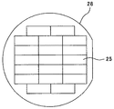
図10は、実施例にかかるウェハに形成した複数の分極前のアクチュエータ基板の配置の一例を示す平面図である。実施例1では、6インチのウェハ28内に40[mm]×20[mm]四方の分極前のアクチュエータ基板25(チップ)が19個配置されている。
FIG. 10 is a plan view illustrating an example of the arrangement of a plurality of unpolarized actuator substrates formed on the wafer according to the example. In the first embodiment, 19 actuator substrates 25 (chips) before polarization in 40 [mm] × 20 [mm] squares are arranged in a 6-
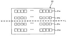
図11は、実施例1にかかる分極前のアクチュエータ基板25の個別電極パッド列の配置をしめす概念図である。本実施例では、4列の液滴吐出部列を備えた液滴吐出ヘッドを形成する。分極前の各アクチュエータ基板25(チップ)内には、図示は省略するが、320個の圧電素子16を列状に並べた4列の圧電素子の列(以下、圧電素子列16a,16b,16c,16dという)が形成されている。この4列の圧電素子列16a,16b,16c,16dに対応する、320個の個別電極パッドを列状に並べた4列の個別電極パッド21の列(以下、個別電極パッド列21a,21b,21c,21dという)と、各列に対応する共通電極パッド(不図示)とを備えている。
FIG. 11 is a conceptual diagram showing the arrangement of the individual electrode pad rows of the
実施例1では、個別電極パッド列21a,21b,21c,21dと平行な分極前のアクチュエータ基板25の中央線Lに対して、個別電極パッド列21a,21b,21c,21dと各共通電極パッド(不図示)とを線対称に配置している。そして、中央線Lに近い内側に位置する個別電極パッド列21b、21cの2列を構成する形成する各個別電極パッド21の表面積を40×40[μm2]とする。また、中央線Lから遠い、基板の外側に位置する個別電極パッド列21a、21dの2列を構成する各個別電極パッド21の表面積を50×50[μm2]とする。共通電極パッド(不図示)の表面積は500×500[μm2]である。このような分極前のアクチュエータ基板25に対して、上述の分極装置を用い、ワイヤー状のコロナ電極が中央線Lの真上となるよう配置して、コロナ放電による分極処理を実施した。コロナ放電の処理条件はコロナワイヤ径50[μm]、電圧は9.0[kV]で実施した。
In the first embodiment, the individual
<実施例2>
実施例2では、分極前のアクチュエータ基板25上で、中央線Lから遠い個別電極パッド列21a、21dの2列の個別電極パッドのサイズを60×60[μm2]とした以外は、実施例1と同様にして分極前のアクチュエータ基板25を作成した。このような、分極前のアクチュエータ基板25に対して、上述の分極装置でワイヤー状のコロナ電極が中央線Lの真上となるよう配置して、コロナ放電による分極処理を実施した。
<Example 2>
In the second embodiment, the size of the individual electrode pads in the two rows of the individual
<実施例3>
実施例3では、実施例1と同様にして分極前のアクチュエータ基板25を作成した。この分極前のアクチュエータ基板25に対して、上述の分極装置でワイヤー状のコロナ電極が分極前のアクチュエータ基板25の中央線Lから個別電極パッド列21b側に2[mm]ずらして配置して、コロナ放電による分極処理を実施した。
<Example 3>
In Example 3, the
<比較例>
比較例では、分極前のアクチュエータ基板25上で、中央線Lから遠い個別電極パッド列21a、21dの2列の個別電極パッドのサイズを、中央線Lから近い個別電極パッド列21b、21cと同じく、40×40[μm2]とした。これ以外は、実施例1と同様にして分極前のアクチュエータ基板25を作成した。このような分極前のアクチュエータ基板25に対して、上述の分極装置でワイヤー状のコロナ電極が中央線Lの真上となるよう配置して、コロナ放電による分極処理を実施した。
<Comparative example>
In the comparative example, the size of the two individual
<結果>
実施例1〜3、比較例に関して分極状態を評価した。具体的には、個別電極パッド列21a,21b,21c,21dに接続された圧電素子列16a,16b,16c,16d(図示は省略)に関して、圧電素子のP−Eヒステリシスループ特性から上述の分極量差(Pr−Pini)を測定した。その結果を図12に示す。また、圧電素子列16a,16b,16c,16dのクラックの発生率について評価した。その結果を図13に示す。
<Result>
The polarization state was evaluated for Examples 1 to 3 and Comparative Example. Specifically, regarding the
実施例1、2、3では、コロナ電極が配置された位置から遠い個別電極パッド列21a、21dの各個別電極パッド21の表面積を、近い個別電極パッド列21b、21cの各個別電極パッド21の表面積に比べて大きくしている。これにより、コロナ電極から遠い個別電極パッド列21a、21dの各個別電極パッド21に供給される電荷量と、近い個別電極パッド列21b、21cの各個別電極パッド21に供給される電荷量を均一化している。その結果、図12に示すように、コロナ電極から遠い位置にある圧電素子列16a,16dにおいても、コロナ電極から近い位置にある圧電素子列16b,16cと同様に、分極量差(Pr−Pini)は3[μC/cm2]程度の低い値となっている。これより、圧電素子列16a,16b,16c,16dに対して良好な分極処理ができていることがわかる。
In Examples 1, 2, and 3, the surface area of each
一方、比較例では、個別電極パッド列21a、21b、21c、21dの各個別電極パッド21の表面積は全て同じ大きさである。このため、コロナ電極から遠い個別電極パッド列21a、21dの各個別電極パッド21に供給される電荷量は、近い個別電極パッド列21b、21cの各個別電極パッド21に供給される電荷量よりも減少する。その結果、図12に示すように、コロナ電極から遠い位置にある圧電素子列16a,16dでは、コロナ電極から近い位置にある圧電素子列16b,16cと分極量差(Pr−Pini)が大きく異なり、高い値となっている。これより、コロナ電極から遠い位置にある圧電素子列16a,16dに対しては、良好な分極処理ができていない。
On the other hand, in the comparative example, the surface areas of the
以上のことから、比較例では、分極前のアクチュエータ基板25上に形成された4列の圧電素子列のうち一括分極処理できるのは2列となるが、実施例1,2,3では、分極前のアクチュエータ基板25上に形成された4列の圧電素子列を一括分極処理できる。このため、分極前のアクチュエータ基板25全体を分割処理する時間を半分に短縮することができる。また、分極前のアクチュエータ基板25を加熱装置により加熱しながら分極処理を行う際、分極処理可能な範囲外では加熱により脱分極が生じてしまい、これにより分極処理の効果が低下してしまうという問題を回避できる。
From the above, in the comparative example, two of the four rows of piezoelectric elements formed on the
さらに、詳細に実施例1〜3について説明する。実施例1、2では、コロナ電極の位置は中央線Lの真上となるよう配置しているため、コロナ電極は中央線Lに対して線対称に配置された各個別電極パッド列21a,21b,21c,21dの中央線と一致する。一方、実施例3では、コロナ電極の位置を中央線Lから個別電極パッド列21b側に2[mm]ずれた位置に配置しており、これが分極量差(Pr−Pini)に影響を与えている。具体的には、圧電素子列16a,16bは、それぞれ、圧電素子列16d,16cに比べて、分極量差(Pr−Pini)が低い値となっている。
Furthermore, Examples 1-3 will be described in detail. In Examples 1 and 2, since the position of the corona electrode is arranged to be directly above the center line L, the individual
次に、圧電素子のクラック発生率について説明する。上述のように圧電素子16の分極処理を行うには所定量の電荷を供給することが必要だが、電荷を供給しすぎるとクラックが発生しやすい。
実施例1〜3、比較例に関して、圧電素子列16a,16b,16c,16dのクラックの発生率について評価した。その結果を図13に示す。
実施例1では、クラック発生率は0%であるが、実施例2では、コロナ電極から遠い位置にある圧電素子列16a,16dにおいて、クラック発生率が15%と大きくなっている。これは、実施例2では、各個別電極パッド列21a,21dの個別電極パッド21を、実施例1よりもさらに大きくしたことで、所望の量以上の電荷が蓄積されたためだと考えられる。
Next, the crack occurrence rate of the piezoelectric element will be described. As described above, it is necessary to supply a predetermined amount of charge in order to perform the polarization process of the
Regarding Examples 1 to 3 and Comparative Example, the occurrence rate of cracks in the
In Example 1, the crack occurrence rate is 0%, but in Example 2, in the
また、実施例3においても、コロナ電極を近づけた圧電素子列16bにおいて、クラック発生率が1%となっている。これも、僅かではあるが、所望の量以上の電荷が蓄積されたためだと考えられる。このため、クラック発生を抑制するためには、個別電極パッド列をコロナ放電電極を配置した中央線に対して線対称に配置することが望ましいといえる。
Also in Example 3, the crack occurrence rate is 1% in the
実施例1〜3では、コロナ電極が配置された位置から遠い個別電極パッド列21a、21dの各個別電極パッド21の表面積を、近い個別電極パッド列21b、21cの各個別電極パッド21の表面積に比べて大きくすることで、広範囲の分極処理を可能とする。なお、個別電極パッド21の大きさについては、分極前のアクチュエータ基板25の大きさ、列の数、分極量差、クラック発生率から最適なサイズを決定すればよく、処理時間の効率化、処理時以外の熱影響を低減することができる。
In the first to third embodiments, the surface area of the
また、実施例1〜3の構成において、コロナ電極が配置された位置から遠い共通電極パッド19の表面積を、近い共通電極パッド19の表面積に比べて大きくすることで、各共通電極パッド19に供給される電荷量を均一化する構成としてもよい。
また、共通電極パッド19の表面積は、すべて同じとしたままでもかまわない。これは、本実施例の構成では、圧電素子列16の共通電極161に接続された共通電極パッド19と、圧電素子列16の各個別電極163に接続された各個別電極パッド21とに供給された電荷が、共通電極161及び各個別電極163に流れ込む。この電荷量の差により、各圧電膜162の内部に電界が形成される。この際、各圧電膜162の個別電極163には個別電極パッド21に供給された電荷がそのまま供給されるが、共通電極パッド19に供給された電荷は複数の圧電膜162に分配される。このため、共通電極パッド19を大きくしても、各圧電膜162の内部に形成される電界に与える影響は、個別電極パッド21を大きくした場合に比べて小さいものと考えられるためである。
このように、共通電極パッド19の大きさについては、分極前のアクチュエータ基板25の大きさ、列の数、分極量差、クラック発生率から最適なものを選択する。
Further, in the configurations of the first to third embodiments, the surface area of the
Further, the
As described above, the optimum size of the
以上説明した、本実施形態のアクチュエータ基板の製造方法によれば、ウェハレベルで、短時間で分極処理をすることができる。例えば、図10に示す複数の分極前のアクチュエータ基板25が配置されたウェハ28を処理する場合は、複数の分極前のアクチュエータ基板25の中央線Lの真上にコロナ電極を配置するよう、ウェハ28を移動させて分極処理を行う。これにより、安定した分極処理が可能となる。
According to the actuator substrate manufacturing method of the present embodiment described above, polarization processing can be performed in a short time at the wafer level. For example, when processing a
また、本実施形態のアクチュエータ基板の製造方法によれば、基板14上の圧電素子16に、第1の絶縁保護膜18、共通電極引き出し配線20、個別電極引き出し配線22、第2の絶縁保護膜23などを形成した後に分極処理をおこなうことができる。このため、第1の絶縁保護膜18、共通電極引き出し配線20、個別電極引き出し配線22、第2の絶縁保護膜23などを形成する工程における熱履歴等による影響による圧電素子の脱分極を回避することができる。
一方、特許文献1に記載された分極処理方法では、圧電膜の表面が露出した状態で分極処理を行う必要がある。そのため、分極処理が実施された圧電素子に、高温の熱処理を伴う、第1の絶縁保護膜18、共通電極引き出し配線20、個別電極引き出し配線22、第2の絶縁保護膜23などを形成する工程が実施されることになる。従って、その後工程での熱履歴等による影響で圧電素子が脱分極し、電気機械変換能の特性が分極処理の前の状態に戻ってしまうおそれがある。
Further, according to the method for manufacturing the actuator substrate of the present embodiment, the first insulating
On the other hand, in the polarization processing method described in Patent Document 1, it is necessary to perform polarization processing with the surface of the piezoelectric film exposed. Therefore, a step of forming the first insulating
この製造方法によって得られるアクチュエータ基板を液滴吐出ヘッドとした場合に、圧電素子16が所定駆動電圧に対して安定した変位量を示し、液滴吐出特性を良好に保持できると共に安定した液滴吐出特性を得ることができることを確認した。
When the actuator substrate obtained by this manufacturing method is used as a droplet discharge head, the
なお、上述の実施形態では、コロナ放電により発生した電荷をもちいて分極処理をおこなう場合を用いて説明したが、グロー放電により発生した電荷をもちいて分極処理をおこなう場合も、同様の構成で、同様の効果が得られる。 In the above-described embodiment, the case where the polarization process is performed using the charges generated by the corona discharge has been described. Similar effects can be obtained.
次に、本実施形態に係る液滴吐出ヘッドを備えた画像形成装置であるインクジェット記録装置について説明する。
図14は、本実施形態の液滴吐出ヘッドを備えたインクジェット記録装置の構成例を示す斜視図であり、図15は同記録装置の機構部の構成例を示す側面図である。
インクジェット記録装置100は、装置本体の内部に印字機構部103等を収納し、装置本体の下方部には前方側から多数枚の記録紙130を積載可能な給紙カセット(或いは給紙トレイでもよい)104を抜き差し自在に装着されている。また、記録紙130を手差しで給紙するために開かれる手差しトレイ105を有している。給紙カセット104あるいは手差しトレイ105から給送される記録紙130を取り込み、印字機構部103によって所要の画像を記録した後、後面側に装着された排紙トレイ106に排紙する。
Next, an ink jet recording apparatus that is an image forming apparatus provided with the droplet discharge head according to the present embodiment will be described.
FIG. 14 is a perspective view illustrating a configuration example of an ink jet recording apparatus including the droplet discharge head according to the present embodiment, and FIG. 15 is a side view illustrating a configuration example of a mechanism unit of the recording apparatus.
The ink
印字機構部103は、主走査方向に移動可能なキャリッジ101とキャリッジ101に搭載した液滴吐出ヘッド及び液滴吐出ヘッドに対してインクを供給するインクカートリッジ102等で構成される。また、印字機構部103は、図示しない左右の側板に横架したガイド部材である主ガイドロッド107と従ガイドロッド108とでキャリッジ101を主走査方向に摺動自在に保持する。このキャリッジ101にはイエロー(Y)、シアン(C)、マゼンタ(M)、ブラック(Bk)の各色のインク滴を吐出する複数のインク吐出口(ノズル)を有する液滴吐出ヘッドを、インク滴吐出方向を下方に向けて装着している。また、キャリッジ101には液滴吐出ヘッドに各色のインクを供給するための各インクカートリッジ102を交換可能に装着している。
The
インクカートリッジ102は上、方に大気と連通する大気口、下方には液滴吐出ヘッドへインクを供給する供給口が設けられている。インクカートリッジ102の内部にはインクが充填された多孔質体を有しており、多孔質体の毛管力により液滴吐出ヘッドへ供給されるインクをわずかな負圧に維持している。また、液滴吐出ヘッドとしては各色のインク滴を吐出するノズルを有する1個の液滴吐出ヘッドを用いている。
The
ここでキャリッジ101は後方側(用紙搬送方向下流側)を主ガイドロッド107に摺動自在に嵌装し、前方側(用紙搬送方向上流側)を従ガイドロッド108に摺動自在に載置している。そして、このキャリッジ101を主走査方向に移動走査するため、主走査モータ109で回転駆動される駆動プーリ110と従動プーリ111との間にタイミングベルト112を張装し、このタイミングベルト112をキャリッジ101に固定している。これにより、主走査モータ109の正逆回転によりキャリッジ101が往復駆動される。
Here, the
一方、給紙カセット104にセットした記録紙130を液滴吐出ヘッドの下方側に搬送するために、給紙カセット104から記録紙130を分離給装する給紙ローラ113及びフリクションパッド114と、記録紙130を案内するガイド部材115とを有する。また、給紙された記録紙130を反転させて搬送する搬送ローラ116と、この搬送ローラ116の周面に押し付けられる搬送コロ117及び搬送ローラ116からの記録紙130の送り出し角度を規定する先端コロ118とを有する。搬送ローラ116は副走査モータによってギヤ列を介して回転駆動される。
On the other hand, in order to convey the
そして、キャリッジ101の主走査方向の移動範囲に対応して搬送ローラ116から送り出された記録紙130を液滴吐出ヘッドの下方側で案内するため用紙ガイド部材である印写受け部材119を設けている。この印写受け部材119の用紙搬送方向下流側には、記録紙130を排紙方向へ送り出すために回転駆動される搬送コロ120と拍車121とを設けている。さらに記録紙130を排紙トレイ106に送り出す排紙ローラ123と拍車124と、排紙経路を形成するガイド部材125,126とを配設している。
In addition, a
上記構成の記録装置100で記録時には、キャリッジ101を移動させながら画像信号に応じて液滴吐出ヘッドを駆動することにより、停止している記録紙130にインクを吐出して1行分を記録し、その後、記録紙130を所定量搬送した後、次の行の記録を行う。記録終了信号または記録紙130の後端が記録領域に到達した信号を受けることにより、記録動作を終了させ記録紙130を排紙する。
When recording with the
また、キャリッジ101の移動方向右端側の記録領域を外れた位置には、液滴吐出ヘッドの吐出不良を回復するための回復装置127を配置している。回復装置127はキャップ手段と吸引手段とクリーニング手段とを有している。キャリッジ101は印字待機中にはこの回復装置127側に移動されてキャッピング手段で液滴吐出ヘッドをキャッピングして吐出口部を湿潤状態に保つことによりインク乾燥による吐出不良を防止する。また、記録途中などに記録と関係しないインクを吐出することにより、全ての吐出口のインク粘度を一定にし、安定した吐出性能を維持する。
In addition, a
吐出不良が発生した場合等には、キャッピング手段で液滴吐出ヘッドの吐出口(ノズル)を密封し、チューブを通して吸引手段で吐出口からインクとともに気泡等を吸い出す。このように、吐出口面に付着したインクやゴミ等はクリーニング手段により除去され吐出不良が回復される。また、吸引されたインクは、本体下部に設置された廃インク溜(不図示)に排出され、廃インク溜内部のインク吸収体に吸収保持される。このように、本実施形態の記録装置100においては回復装置127を備えているので、液滴吐出ヘッドの吐出不良が回復されて、安定したインク滴吐出特性が得られ、画像品質を向上することができる。
When a discharge failure occurs, the capping unit seals the discharge port (nozzle) of the droplet discharge head, and sucks out bubbles and the like from the discharge port through the tube by the suction unit. In this way, ink or dust adhering to the ejection port surface is removed by the cleaning means, and the ejection failure is recovered. Further, the sucked ink is discharged to a waste ink reservoir (not shown) installed at the lower part of the main body and absorbed and held by an ink absorber inside the waste ink reservoir. As described above, since the
なお、本実施形態では、インクジェット記録装置100に液滴吐出ヘッドを使用した場合について説明したが、インク以外の液滴、例えば、パターニング用の液体レジストを吐出する装置に液滴吐出ヘッドを適用してもよい。
In this embodiment, the case where a droplet discharge head is used in the
以上、本実施形態のインクジェット記録装置(画像形成装置)100では、本発明に係る液体吐出ヘッドを記録ヘッドとして備えるので、高画質の画像を安定して形成することができる。 As described above, the ink jet recording apparatus (image forming apparatus) 100 according to the present embodiment includes the liquid discharge head according to the present invention as a recording head, so that a high-quality image can be stably formed.
また、画像形成装置には、特に限定しない限り、シリアル型画像形成装置及びライン型画像形成装置のいずれも含まれる。 Further, the image forming apparatus includes both a serial type image forming apparatus and a line type image forming apparatus, unless otherwise limited.
以上に説明したものは一例であり、本発明は、次の態様毎に特有の効果を奏する。
(態様A)
共通電極161などの下部電極、圧電膜162などの電気機械変換膜、個別電極163などの上部電極とから構成される複数の圧電素子16などの電気機械変換素子を有し、コロナ放電もしくはグロー放電により電気機械変換膜を分極処理してアクチュエータ基板を作成する、分極前のアクチュエータ基板25などの分極処理前基板において、
上記複数の上部電極にそれぞれ電気的に接続された複数の個別電極パッド21などの上部用端子電極を形成し、複数の上部用端子電極が形成された面と対向するよう配置された放電電極で発生させたコロナ放電もしくはグロー放電により上部用端子電極の表面に供給した電荷を用いて上部電極と下部電極との間に電位差を形成して電気機械変換膜の分極処理をおこなうものであり、上部用端子電極の表面積が、放電電極の配置位置から水平方向に関して近い位置よりも遠い位置において大きい。
What has been described above is merely an example, and the present invention has a specific effect for each of the following modes.
(Aspect A)
A corona discharge or a glow discharge has a plurality of electromechanical conversion elements such as a plurality of
Discharge electrodes arranged to form upper terminal electrodes such as a plurality of
(態様A)においては、上記実施形態について説明したように、複数の電気機械変換素子の上部電極に電気的に接続される複数の上部用端子電極が形成された面に対向するよう放電電極を配置する。この放電電極により発生したコロナ放電もしくはグロー放電によって、上部用端子電極の表面に電荷を供給すると、供給された電荷は電気的に接続される上部電極に流れ込んで上部電極に蓄積され、電気機械変換膜を挟んで設けられている下部電極との間に電界を形成する。この電界により電気機械変換膜は分極処理される。
また、複数の上部用端子電極の表面積を、放電電極から水平方向に関して遠い位置において、放電電極から水平方向に関して近い位置よりも大きくしている。このため、放電電極から遠くなるに従って放電が弱くなるコロナ放電もしくはグロー放電を用いても、放電電極から水平方向に関して遠い位置の上部用端子電極の表面に供給される電荷量と、近い位置の上部用端子電極の表面に供給される電荷量を均一化できる。これにより、実施例1〜3で確認されたように、放電電極から遠い位置にある電気機械変換素子に対しても、放電電極から近い位置にある電気機械変換素子と同様に、良好な分極処理が可能となる。よって、複数の電気機械変換素子を備える分極処理前基板において、広範囲の領域に対して安定した一括分極処理が可能となる。
In (Aspect A), as described in the above embodiment, the discharge electrode is disposed so as to face the surface on which the plurality of upper terminal electrodes electrically connected to the upper electrodes of the plurality of electromechanical conversion elements are formed. Deploy. When electric charges are supplied to the surface of the upper terminal electrode by corona discharge or glow discharge generated by this discharge electrode, the supplied electric charge flows into the electrically connected upper electrode and is accumulated in the upper electrode for electromechanical conversion. An electric field is formed between the lower electrode provided across the film. The electromechanical conversion film is polarized by this electric field.
Further, the surface areas of the plurality of upper terminal electrodes are made larger at positions far from the discharge electrodes in the horizontal direction than at positions near the discharge electrodes in the horizontal direction. For this reason, even when using corona discharge or glow discharge, where the discharge becomes weaker as the distance from the discharge electrode increases, the amount of charge supplied to the surface of the upper terminal electrode far from the discharge electrode in the horizontal direction and the upper portion near The amount of charge supplied to the surface of the terminal electrode can be made uniform. As a result, as confirmed in Examples 1 to 3, a favorable polarization treatment was performed on the electromechanical transducer at a position far from the discharge electrode, similarly to the electromechanical transducer at a position near the discharge electrode. Is possible. Therefore, a stable collective polarization process can be performed on a wide area in a pre-polarization substrate including a plurality of electromechanical conversion elements.
(態様B)
(態様A)において、上記複数の個別電極パッド21などの上部用端子電極を列状に並べた個別電極パッド列21a,21b,21c,21dなどの上部用端子電極列を複数有し、上部用端子電極列に沿った中央線Lに対して複数の上部用端子電極列を線対象となるよう配置し、中央線から遠ざかるほど上部用端子電極の表面積が大きい。
これによれば、上記実施形態について説明したように、複数の電気機械変換素子列を備えた構成において分極処理を効率的に行うことができる。さらに、上記中央線L上の放電電極を配置することで、複数の電気機械変換素子列の一部に過剰な電荷が供給されることが避けられ、圧電素子のクラック発生を抑制できる。
(Aspect B)
In (Aspect A), there are a plurality of upper terminal electrode rows such as individual
According to this, as described in the above embodiment, the polarization process can be efficiently performed in the configuration including a plurality of electromechanical transducer element arrays. Furthermore, by disposing the discharge electrode on the center line L, it is possible to avoid excessive charges being supplied to a part of the plurality of electromechanical conversion element arrays, and to suppress the occurrence of cracks in the piezoelectric elements.
(態様C)
(態様A)または(態様B)において、下部電極が複数の電気機械変換素子に共通する共通電極であり、共通電極に電気的に接続される共通電極パッド19などの下部用端子電極を上部用端子電極が形成された面と同じ側に形成し、コロナ放電もしくはグロー放電により下部用端子電極の表面に供給した電荷と、上部用端子電極の表面に供給した電荷とを用いて電気機械変換膜の分極処理をおこなう。
これによれば、上記実施形態について説明したように、下部用端子電極に供給した電荷量と、上部用端子電極の表面に供給した電荷量との差により電気機械変換膜内に電界を形成して分極処理をおこなうことができる。
(Aspect C)
In (Aspect A) or (Aspect B), the lower electrode is a common electrode common to a plurality of electromechanical transducers, and a lower terminal electrode such as a
According to this, as described in the above embodiment, an electric field is formed in the electromechanical conversion film by the difference between the charge amount supplied to the lower terminal electrode and the charge amount supplied to the surface of the upper terminal electrode. Can be polarized.
(態様D)
(態様A)乃至(態様C)の何れかの分極処理前基板に対して、コロナ放電もしくはグロー放電による電荷を供給して上記電気機械変換膜内に電界を発生させて該電気機械変換膜の分極処理をおこなったことを特徴とするアクチュエータ基板。
これによれば、上記実施形態について説明したように、上記構成を有する分極処理前基板をコロナ放電もしくはグロー放電により分極することで、安定した分極特性のアクチェータ基板を得ることができる。また、配線部材などが形成された分極処理前基板に対して分極処理をおこなうことができるため、配線部材などを形成する工程における熱履歴等による影響による電気機械変換膜の脱分極を回避することができ、さらに、安定した分極特性を得ることができる。
(Aspect D)
An electric field is generated in the electromechanical conversion film by supplying a charge by corona discharge or glow discharge to the substrate before polarization treatment of any one of (Aspect A) to (Aspect C). An actuator substrate that has been subjected to polarization treatment.
According to this, as described in the above embodiment, an actuator substrate having a stable polarization characteristic can be obtained by polarizing the pre-polarization substrate having the above configuration by corona discharge or glow discharge. In addition, since the polarization process can be performed on the substrate before the polarization process on which the wiring member or the like is formed, the depolarization of the electromechanical conversion film due to the influence of the thermal history or the like in the process of forming the wiring member or the like is avoided. In addition, stable polarization characteristics can be obtained.
(態様E)
共通電極161などの下部電極、圧電膜162などの電気機械変換膜及び個別電極163などの上部電極を積層した構造の複数の圧電素子16などの電気機械変換素子を備えたアクチュエータ基板の製造方法であって、
基板14上に上記下部電極を形成する工程と、該下部電極上に上記電気機械変換膜を形成する工程と、該電気機械変換膜上に上記上部電極を形成する工程と、該電気機械変換膜と該上部電極とを個別化する工程と、該下部電極上及び該上部電極上に第1の絶縁保護膜18を形成する工程と、該第1の絶縁保護膜上に該下部電極に電気的に接続された共通液室パッド19などの下部用端子電極を形成するとともに、該上部電極に電気的に接続された個別電極パッド21などの上部用端子電極を放電電極が配置される位置から水平方向に関して近い位置よりも、遠い位置において、表面積が大きくなるよう形成する端子電極形成工程と、該下部用端子電極と該上部用端子電極とを露出させた状態で第2の絶縁保護膜23を形成する工程と、該下部用端子電極と該上部用端子電極の表面に、放電電極によりコロナ放電もしくはグロー放電を発生させた電荷を供給して該電気機械変換膜内に電界を発生させて該電気機械変換膜の分極処理をおこなう分極工程とを含む。
これによれば、上記実施形態について説明したように、広範囲の領域に対して安定した一括分極処理が可能となり、分極特性の安定したアクチュエータ基板を効率よく製造することができる。
(Aspect E)
A method of manufacturing an actuator substrate having a plurality of electromechanical transducer elements such as a plurality of
Forming the lower electrode on the substrate, forming the electromechanical conversion film on the lower electrode, forming the upper electrode on the electromechanical conversion film, and the electromechanical conversion film And a step of individualizing the upper electrode, a step of forming a first insulating
According to this, as described in the above embodiment, it is possible to perform a stable collective polarization process over a wide area, and it is possible to efficiently manufacture an actuator substrate having a stable polarization characteristic.
(態様F)
(態様E)において、コロナ放電もしくはグロー放電による電荷として正電荷を用いる。
これによれば、上記実施形態について説明したように、放電により大気中の分子をイオン化させることで、正極性に帯電した電荷を有する陽イオンを容易に発生させることができる。この陽イオンが、共通電極用端子電極、個別電極用端子電極を介して供給されることで、電気機械変換膜の分極処理を安定して行うことができる。
(Aspect F)
In (Embodiment E), a positive charge is used as the charge by corona discharge or glow discharge.
According to this, as described in the above embodiment, positively charged cations can be easily generated by ionizing molecules in the atmosphere by discharge. By supplying this cation through the common electrode terminal electrode and the individual electrode terminal electrode, the polarization treatment of the electromechanical conversion film can be stably performed.
(態様G)
液滴を吐出する複数のノズル11と、ノズルにそれぞれ連通する液室13と、液室内の液体を加圧するためのアクチュエータとを備えた液滴吐出ヘッドにおいて、アクチュエータとして(態様D)のアクチュエータ基板を用いる。これによれば、安定した液滴吐出性能が得られる。
(Aspect G)
In a droplet discharge head including a plurality of
(態様H)
(態様G)の液滴吐出ヘッドを備えたインクジェット記録装置100などの画像形成装置である。これによれば、高品位な画像が得られる。
(Aspect H)
An image forming apparatus such as the
10 液滴吐出部
11 ノズル
12 ノズル基板
13 液室(圧力室)
14 基板(液室基板)
15 振動板
16 圧電素子
161 共通電極(下部電極)
162 圧電膜(圧電体)
163 個別電極(上部電極)
18 第1の絶縁保護膜
18a コンタクトホール
19 共通電極パッド
20 共通電極引き出し配線
21 個別電極パッド
22 個別電極引き出し配線
23 第2の絶縁保護膜
23a 開口部
25 分極前のアクチュエータ基板(分極処理前基板)
28 ウェハ
L 中央線
10 Liquid
14 Substrate (Liquid chamber substrate)
15
162 Piezoelectric film (piezoelectric material)
163 Individual electrode (upper electrode)
DESCRIPTION OF
28 Wafer L Center line
Claims (8)
上記複数の上部電極にそれぞれ電気的に接続された複数の上部用端子電極を形成し、該複数の上部用端子電極が形成された面と対向するよう配置された放電電極で発生させたコロナ放電もしくはグロー放電により該上部用端子電極の表面に供給した電荷を用いて該上部電極と上記下部電極との間に電位差を形成して上記電気機械変換膜の分極処理をおこなうものであり、該上部用端子電極の表面積が、該放電電極の配置位置から水平方向に関して近い位置よりも遠い位置において大きいことを特徴とする分極処理前基板。 A pre-polarization substrate that has a plurality of electromechanical transducer elements composed of a lower electrode, an electromechanical conversion film, and an upper electrode, and creates an actuator substrate by polarizing the electromechanical conversion film by corona discharge or glow discharge In
A plurality of upper terminal electrodes that are electrically connected to the plurality of upper electrodes, respectively, and a corona discharge generated by a discharge electrode disposed to face the surface on which the plurality of upper terminal electrodes are formed. Alternatively, the electromechanical conversion film is polarized by forming a potential difference between the upper electrode and the lower electrode by using electric charges supplied to the surface of the upper terminal electrode by glow discharge. A substrate before polarization treatment, characterized in that the surface area of the terminal electrode for use is larger at a position farther from a position closer to the horizontal direction than an arrangement position of the discharge electrode.
基板上に上記下部電極を形成する工程と、該下部電極上に上記電気機械変換膜を形成する工程と、該電気機械変換膜上に上記上部電極を形成する工程と、該電気機械変換膜と該上部電極とを個別化する工程と、該下部電極上及び該上部電極上に第1の絶縁保護膜を形成する工程と、該第1の絶縁保護膜上に該下部電極に電気的に接続された下部用端子電極を形成するとともに、該上部電極に電気的に接続された上部用端子電極を放電電極が配置される位置から水平方向に関して近い位置よりも、遠い位置において、表面積が大きくなるよう形成する端子電極形成工程と、該下部用端子電極と該上部用端子電極とを露出させた状態で第2の絶縁保護膜を形成する工程と、該下部用端子電極と該上部用端子電極の表面に、放電電極によりコロナ放電もしくはグロー放電を発生させた電荷を供給して該電気機械変換膜内に電界を発生させて該電気機械変換膜の分極処理をおこなう分極工程とを含むアクチュエータ基板の製造方法。 A method of manufacturing an actuator substrate comprising a plurality of electromechanical transducer elements having a structure in which a lower electrode, an electromechanical transducer film and an upper electrode are laminated,
Forming the lower electrode on a substrate, forming the electromechanical conversion film on the lower electrode, forming the upper electrode on the electromechanical conversion film, and the electromechanical conversion film; The step of individualizing the upper electrode, the step of forming a first insulating protective film on the lower electrode and the upper electrode, and the electrical connection to the lower electrode on the first insulating protective film The surface area of the upper terminal electrode electrically connected to the upper electrode is increased at a position farther from the position near the horizontal direction than the position where the discharge electrode is disposed. Forming the terminal electrode, forming the second insulating protective film with the lower terminal electrode and the upper terminal electrode exposed, the lower terminal electrode and the upper terminal electrode The corona is released by the discharge electrode on the surface of Or the actuator substrate manufacturing method comprising a polarization step of an electric field is generated electromechanical conversion film by supplying charges generated glow discharge polarization is performed in the electro-mechanical transducer film.
上記アクチュエータとして、請求項4のアクチュエータ基板を用いたことを特徴とする液滴吐出ヘッド。 In a droplet discharge head comprising a plurality of nozzles for discharging droplets, a liquid chamber communicating with each of the nozzles, and an actuator for pressurizing the liquid in the liquid chamber,
A droplet discharge head using the actuator substrate according to claim 4 as the actuator.
Priority Applications (1)
| Application Number | Priority Date | Filing Date | Title |
|---|---|---|---|
| JP2014039370A JP2015164149A (en) | 2014-02-28 | 2014-02-28 | Pre-polarization processing substrate, actuator substrate, manufacturing method of actuator substrate, droplet discharge head, and image forming apparatus |
Applications Claiming Priority (1)
| Application Number | Priority Date | Filing Date | Title |
|---|---|---|---|
| JP2014039370A JP2015164149A (en) | 2014-02-28 | 2014-02-28 | Pre-polarization processing substrate, actuator substrate, manufacturing method of actuator substrate, droplet discharge head, and image forming apparatus |
Publications (2)
| Publication Number | Publication Date |
|---|---|
| JP2015164149A true JP2015164149A (en) | 2015-09-10 |
| JP2015164149A5 JP2015164149A5 (en) | 2017-01-12 |
Family
ID=54186980
Family Applications (1)
| Application Number | Title | Priority Date | Filing Date |
|---|---|---|---|
| JP2014039370A Pending JP2015164149A (en) | 2014-02-28 | 2014-02-28 | Pre-polarization processing substrate, actuator substrate, manufacturing method of actuator substrate, droplet discharge head, and image forming apparatus |
Country Status (1)
| Country | Link |
|---|---|
| JP (1) | JP2015164149A (en) |
Cited By (1)
| Publication number | Priority date | Publication date | Assignee | Title |
|---|---|---|---|---|
| CN111834321A (en) * | 2019-04-22 | 2020-10-27 | 美科米尚技术有限公司 | Electrical attachment structure and forming method thereof |
Citations (6)
| Publication number | Priority date | Publication date | Assignee | Title |
|---|---|---|---|---|
| JPH05312892A (en) * | 1992-05-14 | 1993-11-26 | Mitsubishi Electric Corp | Corona current measurement |
| JPH08180959A (en) * | 1994-12-20 | 1996-07-12 | Ulvac Japan Ltd | Corona polarization treating method and corona polarization device |
| JPH10286960A (en) * | 1996-10-24 | 1998-10-27 | Seiko Epson Corp | Ink jet recording head and manufacture thereof |
| JP2005262108A (en) * | 2004-03-19 | 2005-09-29 | Fuji Photo Film Co Ltd | Method for manufacturing film-forming apparatus and piezoelectric material |
| JP2013197522A (en) * | 2012-03-22 | 2013-09-30 | Ricoh Co Ltd | Piezoelectric thin film element and method of manufacturing the same, and droplet discharge head using the piezoelectric thin film element, and ink jet recording device |
| JP2013197299A (en) * | 2012-03-19 | 2013-09-30 | Mitsubishi Heavy Ind Ltd | Polarization processing method for oxide-based inorganic piezoelectric material sintered body for ultrasonic thickness sensor, sintered body, and polarization processing device |
-
2014
- 2014-02-28 JP JP2014039370A patent/JP2015164149A/en active Pending
Patent Citations (6)
| Publication number | Priority date | Publication date | Assignee | Title |
|---|---|---|---|---|
| JPH05312892A (en) * | 1992-05-14 | 1993-11-26 | Mitsubishi Electric Corp | Corona current measurement |
| JPH08180959A (en) * | 1994-12-20 | 1996-07-12 | Ulvac Japan Ltd | Corona polarization treating method and corona polarization device |
| JPH10286960A (en) * | 1996-10-24 | 1998-10-27 | Seiko Epson Corp | Ink jet recording head and manufacture thereof |
| JP2005262108A (en) * | 2004-03-19 | 2005-09-29 | Fuji Photo Film Co Ltd | Method for manufacturing film-forming apparatus and piezoelectric material |
| JP2013197299A (en) * | 2012-03-19 | 2013-09-30 | Mitsubishi Heavy Ind Ltd | Polarization processing method for oxide-based inorganic piezoelectric material sintered body for ultrasonic thickness sensor, sintered body, and polarization processing device |
| JP2013197522A (en) * | 2012-03-22 | 2013-09-30 | Ricoh Co Ltd | Piezoelectric thin film element and method of manufacturing the same, and droplet discharge head using the piezoelectric thin film element, and ink jet recording device |
Cited By (2)
| Publication number | Priority date | Publication date | Assignee | Title |
|---|---|---|---|---|
| CN111834321A (en) * | 2019-04-22 | 2020-10-27 | 美科米尚技术有限公司 | Electrical attachment structure and forming method thereof |
| CN111834321B (en) * | 2019-04-22 | 2024-02-13 | 美科米尚技术有限公司 | Method for forming electric adhesion structure |
Similar Documents
| Publication | Publication Date | Title |
|---|---|---|
| JP6478139B2 (en) | Method for manufacturing droplet discharge head | |
| JP6273829B2 (en) | ELECTRO-MACHINE CONVERSION ELEMENT AND MANUFACTURING METHOD THEREOF, AND LIQUID DISCHARGE HEAD HAVING ELECTRO-MECHANICAL CONVERSION ELEMENT, AND LIQUID DISCHARGE EJECTION DEVICE HAVING LIQUID DISCHARGE HEAD | |
| JP6260858B2 (en) | Electromechanical transducer manufacturing method, electromechanical transducer, droplet discharge head, and image forming apparatus | |
| JP2016150471A (en) | Droplet discharge head and image formation device | |
| JP6318793B2 (en) | Electro-mechanical transducer, electro-mechanical transducer manufacturing method, ink jet recording head, and ink jet recording apparatus | |
| JP6079080B2 (en) | Electro-mechanical conversion element manufacturing method, electro-mechanical conversion element, droplet discharge head and droplet discharge apparatus including the electro-mechanical conversion element | |
| JP6304593B2 (en) | Electromechanical conversion member, droplet discharge head, image forming apparatus, and electromechanical conversion element polarization processing method | |
| JP6332735B2 (en) | ELECTRO-MACHINE CONVERSION MEMBER, MANUFACTURING METHOD THEREOF, AND LIQUID DISCHARGE DISCHARGE HEAD AND IMAGE FORMING APPARATUS PROVIDED WITH THE ELECTRO-MACHINE CHANGE MEMBER | |
| JP6112401B2 (en) | Electromechanical conversion element manufacturing method and electromechanical conversion element manufacturing apparatus | |
| JP6414728B2 (en) | Electromechanical conversion member, droplet discharge head, image forming apparatus, polarization processing method of electromechanical conversion element, and method of manufacturing electromechanical conversion member | |
| JP6179804B2 (en) | Electromechanical transducer manufacturing method, electromechanical transducer, droplet ejection head, droplet ejection apparatus, and electromechanical transducer polarization processing apparatus | |
| JP6201461B2 (en) | Polarization equipment | |
| JP6350904B2 (en) | Electromechanical conversion member, droplet discharge head, image forming apparatus, and electromechanical conversion element polarization processing method | |
| JP2015164149A (en) | Pre-polarization processing substrate, actuator substrate, manufacturing method of actuator substrate, droplet discharge head, and image forming apparatus | |
| JP6198118B2 (en) | Electromechanical transducer manufacturing method, electromechanical transducer, droplet ejection head, ink jet recording apparatus, and droplet ejection apparatus | |
| JP6566323B2 (en) | Droplet discharge head, droplet discharge apparatus, and image forming apparatus | |
| JP6132190B2 (en) | Droplet ejection head, liquid ejection device, image forming apparatus, polarization processing method for electromechanical transducer, and method for manufacturing droplet ejection head | |
| JP6198116B2 (en) | Electromechanical transducer manufacturing method, electromechanical transducer, droplet ejection head, droplet ejection apparatus, and image forming apparatus | |
| JP2016164931A (en) | Polarization processing device, droplet discharge head, image forming apparatus, and manufacturing method of electromechanical conversion element | |
| JP2015046434A (en) | Corona polarization processing device, electromechanical conversion element, ink jet recording head, ink jet recording device, and corona polarization processing method | |
| JP6497043B2 (en) | Polarization processing apparatus, droplet discharge head, and image forming apparatus | |
| JP6268985B2 (en) | ELECTRO-MACHINE CONVERSION ELEMENT AND MANUFACTURING METHOD THEREOF, AND LIQUID DISCHARGE HEAD HAVING ELECTRO-MECHANICAL CONVERSION ELEMENT, AND LIQUID DISCHARGE EJECTION DEVICE HAVING LIQUID DISCHARGE HEAD | |
| JP6287178B2 (en) | Electro-mechanical conversion element and droplet discharge head | |
| JP6131653B2 (en) | Electromechanical conversion element, droplet discharge head, and image recording apparatus | |
| JP2015038938A (en) | Discharge device, polarizing processing method, electromechanical conversion element, droplet discharge head, and image formation device |
Legal Events
| Date | Code | Title | Description |
|---|---|---|---|
| A521 | Request for written amendment filed |
Free format text: JAPANESE INTERMEDIATE CODE: A523 Effective date: 20161129 |
|
| A621 | Written request for application examination |
Free format text: JAPANESE INTERMEDIATE CODE: A621 Effective date: 20170207 |
|
| A977 | Report on retrieval |
Free format text: JAPANESE INTERMEDIATE CODE: A971007 Effective date: 20171127 |
|
| A131 | Notification of reasons for refusal |
Free format text: JAPANESE INTERMEDIATE CODE: A131 Effective date: 20171201 |
|
| A521 | Request for written amendment filed |
Free format text: JAPANESE INTERMEDIATE CODE: A523 Effective date: 20180130 |
|
| A02 | Decision of refusal |
Free format text: JAPANESE INTERMEDIATE CODE: A02 Effective date: 20180511 |