JP2015114175A - Inspection apparatus and inspection method - Google Patents
Inspection apparatus and inspection method Download PDFInfo
- Publication number
- JP2015114175A JP2015114175A JP2013255455A JP2013255455A JP2015114175A JP 2015114175 A JP2015114175 A JP 2015114175A JP 2013255455 A JP2013255455 A JP 2013255455A JP 2013255455 A JP2013255455 A JP 2013255455A JP 2015114175 A JP2015114175 A JP 2015114175A
- Authority
- JP
- Japan
- Prior art keywords
- light
- light sources
- inspection
- light source
- imaging
- Prior art date
- Legal status (The legal status is an assumption and is not a legal conclusion. Google has not performed a legal analysis and makes no representation as to the accuracy of the status listed.)
- Pending
Links
Images


Classifications
-
- G—PHYSICS
- G01—MEASURING; TESTING
- G01N—INVESTIGATING OR ANALYSING MATERIALS BY DETERMINING THEIR CHEMICAL OR PHYSICAL PROPERTIES
- G01N21/00—Investigating or analysing materials by the use of optical means, i.e. using sub-millimetre waves, infrared, visible or ultraviolet light
- G01N21/84—Systems specially adapted for particular applications
- G01N21/88—Investigating the presence of flaws or contamination
- G01N21/8806—Specially adapted optical and illumination features
- G01N2021/8812—Diffuse illumination, e.g. "sky"
- G01N2021/8816—Diffuse illumination, e.g. "sky" by using multiple sources, e.g. LEDs
-
- G—PHYSICS
- G01—MEASURING; TESTING
- G01N—INVESTIGATING OR ANALYSING MATERIALS BY DETERMINING THEIR CHEMICAL OR PHYSICAL PROPERTIES
- G01N21/00—Investigating or analysing materials by the use of optical means, i.e. using sub-millimetre waves, infrared, visible or ultraviolet light
- G01N21/84—Systems specially adapted for particular applications
- G01N21/88—Investigating the presence of flaws or contamination
- G01N21/8806—Specially adapted optical and illumination features
- G01N2021/8829—Shadow projection or structured background, e.g. for deflectometry
- G01N2021/8832—Structured background, e.g. for transparent objects
-
- G—PHYSICS
- G01—MEASURING; TESTING
- G01N—INVESTIGATING OR ANALYSING MATERIALS BY DETERMINING THEIR CHEMICAL OR PHYSICAL PROPERTIES
- G01N21/00—Investigating or analysing materials by the use of optical means, i.e. using sub-millimetre waves, infrared, visible or ultraviolet light
- G01N21/84—Systems specially adapted for particular applications
- G01N21/88—Investigating the presence of flaws or contamination
- G01N21/8806—Specially adapted optical and illumination features
- G01N2021/8845—Multiple wavelengths of illumination or detection
Landscapes
- Physics & Mathematics (AREA)
- Health & Medical Sciences (AREA)
- Life Sciences & Earth Sciences (AREA)
- Chemical & Material Sciences (AREA)
- Analytical Chemistry (AREA)
- Biochemistry (AREA)
- General Health & Medical Sciences (AREA)
- General Physics & Mathematics (AREA)
- Immunology (AREA)
- Pathology (AREA)
- Length Measuring Devices By Optical Means (AREA)
- Investigating Materials By The Use Of Optical Means Adapted For Particular Applications (AREA)
Abstract
【課題】一例として、検査面の形状不良を検出しやすい新規な検査装置を得る。【解決手段】実施形態の検査装置1は、照明装置2と、撮像装置3と、検出部と、を備えている。照明装置2は、三つ以上の光源4のうち三つ以上の光源4の並び方向で一端に位置する光源4の光の照射領域と、三つ以上の光源4のうち三つ以上の光源4の並び方向で他端に位置する光源4の光の照射領域と、に亘って二つ以上の光源4の光の照射領域が相互に重なる。撮像装置3は、照明装置2とともに検査面100aに対して相対移動されながら、照明装置2によって照明された検査面100aを撮像する。検出部は、撮像装置3の撮像によって得られた画像から特定される撮像装置3が受光した光の組み合わせを用いて、撮像装置3が受光した光の出射位置を特定し、特定した出射位置を用いて検査面100aの形状不良を検出する。【選択図】図1As an example, a novel inspection apparatus that easily detects a shape defect of an inspection surface is obtained. An inspection apparatus according to an embodiment includes an illumination device, an imaging device, and a detection unit. The illuminating device 2 includes a light irradiation region of the light source 4 positioned at one end in the arrangement direction of the three or more light sources 4 among the three or more light sources 4, and three or more light sources 4 of the three or more light sources 4. The light irradiation regions of the two or more light sources 4 overlap each other over the light irradiation region of the light source 4 located at the other end in the arrangement direction. The imaging device 3 images the inspection surface 100 a illuminated by the illumination device 2 while being moved relative to the inspection surface 100 a together with the illumination device 2. The detection unit specifies an emission position of light received by the imaging device 3 using a combination of light received by the imaging device 3 specified from an image obtained by imaging of the imaging device 3, and determines the specified emission position. It is used to detect a shape defect of the inspection surface 100a. [Selection] Figure 1
Description
本発明は、検査装置および検査方法に関する。 The present invention relates to an inspection apparatus and an inspection method.
従来、光を照射した検査面を撮像し、撮像で得た画像に基づいて該検査面の形状不良を検出する検査装置が知られている。 2. Description of the Related Art Conventionally, an inspection apparatus that captures an image of an inspection surface irradiated with light and detects a shape defect of the inspection surface based on an image obtained by imaging is known.
この種の検査装置として、例えば、RGBの幅がそれぞれ異なる明暗パターンを作成し、各波長の画像に周波数フィルタを適用し、所定の周波数とは異なる周期で明暗パターンが変化している部分を強調し、閾値を用いて不良を検出するものがある。 As this type of inspection device, for example, create a light / dark pattern with different RGB widths, apply a frequency filter to the image of each wavelength, and emphasize the portion where the light / dark pattern changes at a period different from the predetermined frequency Some of them detect a defect using a threshold value.
この種の検査装置では、検査面の不良を検出しやすい新規な構成が望まれている。 In this type of inspection apparatus, a new configuration that easily detects defects on the inspection surface is desired.
そこで、本発明は、一例としては、検査面の形状不良を検出しやすい新規な検査装置および検査方法を得ることを目的の一つとする。 Thus, as an example, an object of the present invention is to obtain a novel inspection apparatus and inspection method that can easily detect a shape defect of an inspection surface.
本発明の実施形態にかかる検査装置は、三つ以上の光源を有し、検査面に対して相対移動されながら前記三つ以上の光源によって前記検査面を照明し、前記三つ以上の光源が前記相対移動方向で相互に異なる位置に位置し、隣り合う前記光源が出射する光の波長が相互に異なり、隣り合う前記光源の光の照射領域の一部が相互に重なることで、前記三つ以上の光源のうち前記三つ以上の光源の並び方向で一端に位置する前記光源の光の照射領域と、前記三つ以上の光源のうち前記三つ以上の光源の並び方向で他端に位置する前記光源の光の照射領域と、に亘って二つ以上の前記光源の光の照射領域が相互に重なった、照明装置と、前記照明装置とともに前記検査面に対して相対移動されながら、前記照明装置によって照明された前記検査面を撮像する撮像装置と、前記撮像装置の撮像によって得られた画像から特定される前記撮像装置が受光した光の組み合わせを用いて、前記撮像装置が受光した光の出射位置を特定し、特定した前記出射位置を用いて前記検査面の不良を検出する検出部と、を備えた。 An inspection apparatus according to an embodiment of the present invention has three or more light sources, illuminates the inspection surface with the three or more light sources while being relatively moved with respect to the inspection surface, and the three or more light sources are The wavelengths of light emitted from adjacent light sources that are located at different positions in the relative movement direction are different from each other, and part of the light irradiation regions of the adjacent light sources overlap each other. Among the light sources described above, the light irradiation region of the light source located at one end in the direction in which the three or more light sources are arranged, and the other end in the direction in which the three or more light sources are arranged among the three or more light sources The light irradiation region of the light source that overlaps the light irradiation region of two or more of the light sources, the illumination device and the relative movement with respect to the inspection surface together with the illumination device, The inspection surface illuminated by the illumination device An emission position of light received by the imaging device is identified and identified using a combination of an imaging device to be imaged and light received by the imaging device identified from an image obtained by imaging of the imaging device. And a detection unit that detects a defect of the inspection surface using the emission position.
また、本発明の実施形態にかかる検査方法は、三つ以上の光源を有し、検査面に対して相対移動されながら前記三つ以上の光源によって前記検査面を照明し、前記三つ以上の光源が前記相対移動方向で相互に異なる位置に位置し、隣り合う前記光源が出射する光の波長が相互に異なり、隣り合う前記光源の光の照射領域の一部が相互に重なることで、前記三つ以上の光源のうち前記三つ以上の光源の並び方向で一端に位置する前記光源の光の照射領域と、前記三つ以上の光源のうち前記三つ以上の光源の並び方向で他端に位置する前記光源の光の照射領域と、に亘って二つ以上の前記光源の光の照射領域が相互に重なった、照明装置を備えた検査装置において実行される検査方法であって、撮像装置が、前記照明装置とともに前記検査面に対して相対移動されながら、前記照明装置によって照明された前記検査面を撮像する工程と、検出部が、前記撮像装置の撮像によって得られた画像から特定される前記撮像装置が受光した光の組み合わせを用いて、前記撮像装置が受光した光の出射位置を特定し、特定した前記出射位置を用いて前記検査面の不良を検出する工程と、を含む。 Further, the inspection method according to the embodiment of the present invention includes three or more light sources, illuminates the inspection surface with the three or more light sources while being relatively moved with respect to the inspection surface, and the three or more light sources. The light sources are located at different positions in the relative movement direction, the wavelengths of light emitted by the adjacent light sources are different from each other, and a part of the light irradiation region of the adjacent light sources overlaps each other, Among the three or more light sources, the light irradiation region of the light source positioned at one end in the direction in which the three or more light sources are arranged, and the other end in the direction in which the three or more light sources are arranged among the three or more light sources A light irradiation region of the light source located at a position where two or more light irradiation regions of the light source overlap each other, the inspection method being executed in an inspection device including an illumination device, A device is mounted on the inspection surface together with the illumination device. A step of imaging the inspection surface illuminated by the illuminating device while being relatively moved, and a combination of light received by the imaging device identified by the detection unit from an image obtained by imaging of the imaging device. And a step of specifying an emission position of light received by the imaging device and detecting a defect of the inspection surface using the specified emission position.
本発明によれば、一例として、検査面の形状不良を検出しやすい新規な検査装置および検査方法を得ることができる。 According to the present invention, as an example, it is possible to obtain a novel inspection apparatus and inspection method that can easily detect a shape defect of an inspection surface.
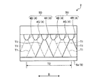
図1に示すように、本実施形態の検査装置1は、照明装置2と撮像装置3とを備えている。照明装置2と撮像装置3とは、移動装置30(図7)によって、検査対象である検査物100の検査面100aに対して相対移動される。検査装置1は、照明装置2によって光を照射した検査面100aの画像を撮像装置3によって撮像し、その撮像によって得られた画像を用いて、検査面100aの形状不良を検出する。本実施形態では、一例として、照明装置2が、検査面100aに対する照明装置2および撮像装置3の移動方向Fで、撮像装置3の前方に位置している。
As shown in FIG. 1, the
移動装置30は、一例として、照明装置2と撮像装置3とを一体に支持している。移動装置30は、一例として、モータ等の駆動源を有しており、駆動源の駆動力によって、照明装置2と撮像装置3とを、位置固定された検査面100aに沿って移動させる。なお、移動装置30は、検査物100を支持して、検査物100を、位置固定された照明装置2と撮像装置3とに対して移動させる構成であってもよい。
As an example, the
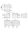
照明装置2は、複数の光源4を有し、検査面100aに対して相対移動されながらそれらの光源4によって検査面100aを照明する。本実施形態では、一例として、光源4は、六つ設けられている。つまり、本実施形態では、光源4は、三つ(四つ)以上設けられている。各光源4は、移動方向F(相対移動方向)で相互に異なる位置に位置している。各光源4は、移動方向Fと交差(一例として直交)する方向(図1での紙面と直交する方向)に延在した帯状(ライン状)の光を照射する。各光源4は、一例として、照明装置2の移動方向Fと直交する方向に沿って配置された複数のLED(Light Emitting Diode)を有し、移動方向Fと直交する方向に延在した帯状(ライン状)の照明光を出射する。また、本実施形態では、照明装置2は、光源4として、出射する光の波長(波長域)が相互に異なる三種類以上、一例として三種類の光源4R,4G,4Bを有している。光源4Rは、赤色(R)の光を出射し、光源4Gは、緑色(G)の光を出射し、光源4Bは、青色(B)の光を出射する。
The
また、本実施形態では、光源4R,4G,4Bの組が二組設けられており、一方の組の、光源4R、光源4G、光源4B、他方の組の、光源4R、光源4G、光源4Bが、この順で移動方向Fの上流側から下流側に向けて配置されている。つまり、本実施形態では、隣り合う光源4が出射する光の波長が相互に異なる。また、一方の組の光源4R,4G,4Bは、光源部5Uを構成し、他方の組の光源4R,4G,4Bは、光源部5Dを構成している。このように、本実施形態では、四つ以上(一例として、六つ)の光源4が、出射する光の波長が相互に異なる複数(一例として三つ)の光源4R,4G,4Bをそれぞれ有し相互に隣り合って位置した二つの光源部5D,5Uを構成している。また、二つの光源部5D,5Uは、光源4の種類の組み合わせと光源4の並び順とが相互に同じである。なお、本実施形態では、出射する光の波長が相互に異なる複数の光源4として、三つの光源4R,4G,4Bの例を示したが、出射する光の波長が相互に異なる光源4は、例えば四つ以上であってもよい。
In this embodiment, two sets of
また、本実施形態では、照明装置2は、一例として、拡散板6を有している。拡散板6は、光源4における光の出射側に位置し、各光源4と対向している。拡散板6は、光源4とは反対側の出光面6a(面)を有している、光源から出射された光は、拡散板6によって拡散されて出光面6aから出光し、検査面100aを照明する。拡散板6の出光面6aは、照明装置2の出光面を構成する。
Moreover, in this embodiment, the
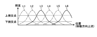
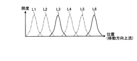
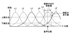
以上の構成の照明装置2では、図2に示すように、拡散板6の出光面6a上において、隣り合う光源4の光の照射領域T1(出光領域、領域)の一部が相互に重なる。この重なりによって、照明装置2は、拡散板6の出光面6a上において、複数の光源4のうち複数の光源4の並び方向Bで一端に位置する光源4(一例として、光源部5Uの光源4R)の光の照射領域T1と、複数の光源4のうち複数の光源4の並び方向Bで他端に位置する光源4(一例として、光源部5Dの光源4B)の光の照射領域T1と、に亘って二つ以上の光源4の光の照射領域T1が相互に重なった、重複領域T2を有する。かかる構成により、本実施形態では、全ての光源4が点灯した場合の拡散板6の出光面6a上における光の照度分布(配光特性)は、一例として、図3に示すようになる。ここで、図3の横軸は、出光面6a上での位置を示し、縦軸は、照度を示している。また、図3中の照度分布線L1〜L3は、光源部5Dの光源4B、光源4G、光源4Rに対応し、照度分布線L4〜L6は、光源部5Uの光源4B、光源4G、光源4Rに対応している。出光面6a上での位置は、複数の光源4の並び方向B(図2)での位置である。図3に示すように、各光源4の照度は、光源4の山形状の分布となり、重複領域T2に対応した出光面6aの領域では、少なくとも隣り合う光源4から出射された光の一部同士が重なる。このとき、山形状の照度分布の頂部となる光の部位同士は重ならない。以上から分かるように、照明装置2は、光源4が出射する光を拡散板6で拡散してエリア照明光として出射するエリア照明装置として構成されている。
In the illuminating
図1に一例を示す撮像装置3は、照明装置2とともに検査面100aに対して相対移動されながら、照明装置2によって照明された検査面100aを撮像する。撮像装置3は、照明装置2とともに検査面100aに対して相対移動されながら、一例として、照明装置2から出射された光の検査面100aでの反射光を受光する。撮像装置3は、一例として、検査面100aでの正反射光を受光する。撮像装置3は、一例として、ラインカメラ(ラインセンサ)として構成されている。撮像装置3は、検査面100aとの相対移動方向と直交する方向であって光源4の帯状の照明光の延在方向に沿って一列に配置された複数の光電変換素子(撮像素子、図示せず)を有している。すなわち、撮像装置3は、検査面100aとの相対移動方向と直交する方向に沿った線状の画像(画像データ、撮像データ、各光電変換素子に対応した画素毎の輝度値のデータ、輝度値のデータ列)を取得する。各撮像素子では、例えば256階調で輝度値のデータが取得される。撮像装置3は、一例として、各撮像素子について複数(例えば、赤色(R)、緑色(G)、青色(B)の三つ)の画像データを取得可能である。
The
撮像装置3は、図1,4に示すように、検査面100aに向かう撮像方向D1(撮像装置3の光軸、視線、図4)に位置する検査面100aの撮像領域Aを撮像する。この場合、本実施形態では、撮像装置3は、照明装置2から出射され検査面100aで正反射した光(正反射光)を受光する。つまり、本実施形態では、撮像装置3の検査面100aを介しての撮像方向D2(視線、図4)は、検査面100aの法線に対する、撮像装置3の検査面100aに向かう撮像方向D1と等角をなす方向である。
As shown in FIGS. 1 and 4, the
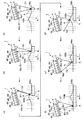
撮像装置3の検査面100aを介しての撮像方向D2は、一例として、図4に示すように、検査面100aの形状に応じて変化する。図4は、検査面100aに形状不良としての凸部100bがある検査面100aに対する検査装置1の変位を(a)〜(e)に順を追って示している。
As an example, the imaging direction D2 through the
図4の(a)は、撮像領域Aが、移動方向Fで凸部100bの上流側(後方)に位置する検査面100aの平坦な領域(正常部分)に位置し、撮像方向D2が、出光面6aの部位6a1に向かう方向となった場合を示している。
4A, the imaging region A is located in a flat region (normal portion) of the
図4の(b)は、撮像領域Aが、移動方向Fに対する上り斜面(上り勾配)を構成する凸部100bの領域中に位置し、撮像方向D2が、出光面6aにおける部位6a1よりも移動方向Fの上流側の部位6a2に向かう方向となった場合を示している。
In FIG. 4B, the imaging region A is located in the region of the
図4の(c)は、撮像領域Aが、移動方向Fに対して上り斜面(上り勾配)を構成する凸部100bの領域において、図4の(b)よりも急勾配な部位に位置し、撮像方向D2が、出光面6aから移動方向Fの上流側に外れた方向となった場合を示している。
4C, the imaging region A is located at a steeper portion than the portion (b) of FIG. 4B in the region of the
図4の(d)は、撮像領域Aが、移動方向Fに対して下り斜面(下り勾配)を構成する凸部100bの領域中に位置し、撮像方向D2が、出光面6aから移動方向Fの下流側(前方)に外れた方向となった場合を示している。
4D, the imaging region A is located in the region of the
図4の(e)は、撮像領域Aが、移動方向Fに対して下り斜面(下り勾配)を構成する凸部100bの領域において図4の(d)よりも緩勾配な位置に位置し、撮像方向D2が、出光面6aにおける部位6a1よりも移動方向Fの下流側の部位6a3に向かう方向となった場合を示している。
4 (e), the imaging region A is located at a gentler slope than the position (d) of FIG. 4 in the region of the
図4の(f)は、撮像領域Aが、移動方向Fで凸部100bの下流側に位置する検査面100aの平坦な領域(正常部分)に位置し、撮像方向D2が、出光面6aの部位6a1に向かう方向に戻った場合を示している。
4F, the imaging region A is located in a flat region (normal portion) of the
撮像装置3が撮像する画像ILは、撮像方向D2に存在する光を受けた画像となる。したがって、一例として、撮像方向D2に出光面6aがある場合には、その撮像方向D2に対応する出光面6a上の領域から出光して検査面100aで正反射した光が撮像され、撮像方向D2が出光面6aから外れている場合には、出光面6aから出光して検査面100aで正反射した光は撮像されない。つまり、本実施形態では、検査面100aに凸状や凹状の形状不良があると、撮像装置3が撮像(受光)する光の組み合わせが変化することとなる。図4の(a)の場合に撮像される画像ILでは、赤色の輝度値と青色の輝度値とが、所定の値以上となり且つ緑色の輝度値よりも高くなる。また、図4の(b)の場合に撮像される画像ILでは、赤色の輝度値と緑色の輝度値とが、所定の値以上となり且つ青色の輝度値よりも高くなる。また、図4の(c),(d)の場合に撮像される画像ILでは、赤色、緑色および青色の輝度値が、それぞれ所定の値未満となる。また、図4の(e)の場合に撮像される画像ILでは、青色の輝度値が、所定の値以上となり且つ赤色の輝度値および緑色の輝度値よりも高くなる。また、図4の(f)の場合に撮像される画像ILでは、赤色の輝度値と青色の輝度値とが、所定の値以上となり且つ緑色の輝度値よりも高くなる。
The image IL captured by the
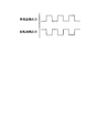
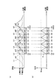
また、本実施形態では、一例として、図1に示すように、検査装置1は、発振回路7と、発振回路7に接続された反転回路8と、発振回路7と光源部5Dとの間に介在した電源9Dと、反転回路8と光源部5Uとの間に介在した電源9Uと、を備えている。また、反転回路8には、撮像装置3が接続されている。図5に示すように、発振回路7が出力する信号は、基準クロック信号であり、反転回路8が出力する信号は、基準クロック信号の反転信号である。電源9Dは、発振回路7から出力された基準クロック信号に基づいて光源部5Dへの電力の供給および停止を切り替え、電源9Uは、反転回路8から出力された反転信号に基づいて光源部5Uへの電力の供給および停止を切り替える。また、撮像装置3は、反転回路8から出力された反転信号に基づいて撮像を行う。
In the present embodiment, as an example, as shown in FIG. 1, the
上記構成により、本実施形態では、光源部5D,5Uによる検査面100aへの光の照射は、交互に行われる。すなわち、光源部5Dが照明しているときは、光源部5Uによる照明は行われない。また、光源部5Uが照明しているときは、光源部5Dによる照明は行われない。そして、撮像装置3による撮像(画像の取得)と、光源部5D,5Uによる検査面100aへの光の照射(一例として、光源部5D,5Uの発光の切り替え)とが同期されている。すなわち、本実施形態では、一例として、図6に示されるように、撮像装置3は、光源部5Dからの光で照らされている際の検査面100aの一次元の画像IL1(第一画像、線状画像、画像データ)と、光源部5Uからの光で照らされている際の検査物100の一次元の画像IL2(第二画像、線状画像、画像データ)とを、交互に所定回数ずつ撮像して画像I(画像データ)を取得する。制御部20(図7参照)は、光源部5Dからの光で照らされている際の検査物100の画像IL1を取得した順に並べて二次元の画像IA1(第一画像、画像データ、二次元に配列された輝度値のデータ群)を得ることができるとともに、光源部5Uからの光で照らされている際の検査物100の画像IL2を所定期間内で取得した順に並べて二次元の画像IA2(第二画像、画像データ、二次元に配列された輝度値のデータ群)を得ることができる。また、制御部20は、画像IA1をRGB分解して、赤色(R)成分に対応する画像IR1と、緑色(G)成分に対応する画像IG1と、青色(B)成分に対応する画像IB1と、を取得することができる。また、制御部20は、画像IA2をRGB分解して、赤色(R)成分に対応する画像IR2と、緑色(G)成分に対応する画像IG2と、青色(B)成分に対応する画像IB2と、を取得することができる。更に、制御部20は、画像IA1と画像IA2とを合成して画像ICを取得することができる。ここで、光源部5D,5Uによる照明の切り替えの周波数、すなわち撮像装置3によるライン毎の撮像の周波数は、比較的高い値に設定される。よって、画像IA1,IA2は、検査面100aの略同一部位の画像とみなして、画像IA1と画像IA2とが合成される。詳細には、画像IA1のN行目(Nは整数)の画像IL1と、画像IA2のN行目の画像IL2とが合成される。本実施形態では、以上により得られた各画像IR1,IG1,IB1,IR2,IG2,IB2,ICは、検査面100aの同一部位の画像として処理される。以上から分かるように、本実施形態では、撮像装置3の各ラインの撮像では、同じ波長の光源4同士の照明光が混在しないように、相互に異なる波長の光源4が点灯する。
With the above configuration, in the present embodiment, the light irradiation to the
また、本実施形態では、一例として、図7に示すように、検査装置1は、制御部20(例えばCPU(Central Processing Unit)等)や、ROM21(Read Only Memory)、RAM22(Random Access Memory)、SSD23(Solid State Drive)、光照射コントローラ24、撮像コントローラ25、移動コントローラ26、表示コントローラ27等を備えている。光照射コントローラ24は、制御部20からの制御信号に基づいて、照明装置2の発光等を制御する。撮像コントローラ25は、制御部20からの制御信号に基づいて、撮像装置3による撮像を制御する。本実施形態では、一例として、光照射コントローラ24は、発振回路7、反転回路8、電源9D,9Uを含んで構成され、撮像コントローラ25は、反転回路8を含んで構成されている。また、移動コントローラ26は、制御部20から受けた制御信号に基づいて、移動装置30を制御し、照明装置2および撮像装置3の移動(開始、停止、速度等)を制御する。表示コントローラ27は、制御部20からの制御信号に基づいて、表示装置40(例えば、LCD(Liquid Crystal Display)、OELD(Organic Electro-Luminescence Display)等)を制御する。つまり、制御部20は、光照射コントローラ24、撮像コントローラ25、移動コントローラ26、表示コントローラ27を介して、照明装置2、撮像装置3、移動装置30、表示装置40を制御する。
In the present embodiment, as an example, as illustrated in FIG. 7, the
また、制御部20は、不揮発性の記憶部としてのROM21やSSD23等にインストールされたプログラム(アプリケーション)を読み出して実行する。RAM22は、制御部20がプログラムを実行して種々の演算処理を実行する際に用いられる各種データを一時的に記憶する。なお、図7に示されるハードウエアの構成はあくまで一例であって、例えばチップやパッケージにする等、種々に変形して実施することが可能である。また、各種演算処理は、並列処理することが可能であり、制御部20等は、並列処理が可能なハードウエア構成とすることが可能である。
Further, the
本実施形態では、一例として、SSD23(記憶部)は、出射位置特定用情報を記憶している。出射位置特定用情報は、撮像装置3が受光する光の組み合わせと、複数の光源4の並び方向B(図2参照)に規定された照明装置2による光の出射位置に対応した位置座標との関係を示す情報を含む。
In the present embodiment, as an example, the SSD 23 (storage unit) stores emission position specifying information. The emission position specifying information includes a combination of light received by the
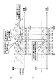
以下に、図8を参照して出射位置特定用情報について説明する。まず、本実施形態では、一例として、各光源4にチャンネルch(チャンネル番号)が割り当てられている。光源部5Dの光源4B、光源4G、光源4Rには、それぞれチャンネルch1、チャンネルch2、チャンネルch3が割り当てられ、光源部5Uの光源4B、光源4G、光源4Rには、それぞれチャンネルch4、チャンネルch5、チャンネルch6が割り当てられている。
The emission position specifying information will be described below with reference to FIG. First, in this embodiment, as an example, a channel ch (channel number) is assigned to each
図8の(a)に示すように、各チャンネルch1〜ch6(すなわち、光源部5Dの光源4B、光源4G、光源4R、光源部5Uの光源4B、光源4G、光源4R)に対応した拡散板6の出光面6aにおける照度分布を示す照度分布線L1〜L6同士は、交点P1〜P9で交わる。なお、図8の(a)は、図3と同様に、横軸が出光面6a上での位置に対応した位置座標を示し、縦軸が照度を示している。交点P1は、チャンネルch1の照度分布線L1とチャンネルch2の照度分布線L2との交点である。交点P2は、チャンネルch1の照度分布線L1とチャンネルch3の照度分布線L3との交点である。交点P3は、チャンネルch2の照度分布線L2とチャンネルch3の照度分布線L3との交点である。交点P4は、チャンネルch2の照度分布線L2とチャンネルch4の照度分布線L4との交点である。交点P5は、チャンネルch3の照度分布線L3とチャンネルch4の照度分布線L4との交点である。交点P6は、チャンネルch3の照度分布線L3とチャンネルch5の照度分布線L5との交点である。交点P7は、チャンネルch4の照度分布線L4とチャンネルch5の照度分布線L5との交点である。交点P8は、チャンネルch4の照度分布線L4とチャンネルch6の照度分布線L6との交点である。交点P9は、チャンネルch5の照度分布線L5とチャンネルch6の照度分布線L6との交点である。交点P1,P3,P5,P7,P9は、上側交点であり、交点P2,P4,P6,P8は、下側交点であり、上側交点での照度よりも下側交点での照度の方が低くなっている。なお、以下では、交点P1〜P9を、nを整数として、P(n)とも表す。また、本実施形態では、交点P1〜P9の座標位置は、それぞれC0〜C9と表される。なお、C0〜C9を、nを整数として、C(n)とも表す。
As shown in FIG. 8A, diffusion plates corresponding to the channels ch1 to ch6 (that is, the
また、本実施形態では、交点P1〜交点P8の間の座標位置に規定の階調が割り当てられている。本実施形態では、一例として、交点P1の座標位置(C0)と交点P8の座標位置(C8)との間に0〜1023の階調が割り当てられている。また、各交点P1〜P2間の距離が階調数で算出されている。交点P1と交点P2との間の階調数(距離)は、ST1で表され、交点P2と交点P3との間の階調数は、ST2で表され、交点P3と交点P4との間の階調数は、ST3で表され、交点P4と交点P5との間の階調数は、ST4で表され、交点P5と交点P6との間の階調数は、ST5で表され、交点P6と交点P7との間の階調数は、ST6で表され、交点P7と交点P8との間の階調数は、ST7で表され、交点P8と交点P9との間の階調数は、ST8で表される。なお、ST1〜ST8を、nを整数として、ST(n)とも表す。以上から、ST(n)=C(n)−C(n−1)と表せる。 In the present embodiment, a specified gradation is assigned to the coordinate position between the intersection points P1 to P8. In the present embodiment, as an example, gradations of 0 to 1023 are assigned between the coordinate position (C0) of the intersection point P1 and the coordinate position (C8) of the intersection point P8. Further, the distance between the intersections P1 and P2 is calculated by the number of gradations. The number of gradations (distance) between the intersection P1 and the intersection P2 is represented by ST1, and the number of gradations between the intersection P2 and the intersection P3 is represented by ST2 between the intersection P3 and the intersection P4. The number of gradations is represented by ST3, the number of gradations between the intersection P4 and the intersection P5 is represented by ST4, the number of gradations between the intersection P5 and the intersection P6 is represented by ST5, and the intersection P6. The number of gradations between the intersection P7 and the intersection P7 is represented by ST6, the number of gradations between the intersection P7 and the intersection P8 is represented by ST7, and the number of gradations between the intersection P8 and the intersection P9 is It is represented by ST8. ST1 to ST8 are also expressed as ST (n), where n is an integer. From the above, it can be expressed as ST (n) = C (n) −C (n−1).
また、本実施形態では、下側交点(交点P2,P4,P6,P8)での照度に対する、該下側交点の座標位置での最大照度を示すチャンネルchの照度の倍率(比率、下側交点倍率)が算出されて、この倍率が最大倍率として規定されている。なお、図8等で最大倍率は、Mmaxで表されている。また、上側交点(交点P1,P3,P5,P7,P9)で照度分布線L1〜L6が交わるチャンネルch1〜ch6同士の倍率(上側交点倍率)は、1であり、この倍率が基準倍率として規定されている。そして、上側交点(交点P2,P4,P6,P8)での座標位置での基準倍率と下側交点での座標位置での最大倍率とを直線で結んだ倍率線R(図8の(b))が取得されている。倍率線Rは、三角波状となっている。 In the present embodiment, the illuminance magnification (ratio, lower intersection) of the channel ch indicating the maximum illuminance at the coordinate position of the lower intersection with respect to the illuminance at the lower intersection (intersections P2, P4, P6, P8). (Magnification) is calculated, and this magnification is defined as the maximum magnification. In FIG. 8 and the like, the maximum magnification is represented by Mmax. Further, the magnification (upper intersection magnification) between the channels ch1 to ch6 where the illuminance distribution lines L1 to L6 intersect at the upper intersections (intersections P1, P3, P5, P7, P9) is 1, and this magnification is defined as a reference magnification. Has been. Then, a magnification line R ((b) in FIG. 8) connecting the reference magnification at the coordinate position at the upper intersection (intersection points P2, P4, P6, P8) and the maximum magnification at the coordinate position at the lower intersection at a straight line. ) Has been acquired. The magnification line R has a triangular wave shape.
また、本実施形態では、一例として、制御部20は、ハードウエアとソフトウエア(プログラム)との協働によって、検査装置1の少なくとも一部として機能(動作)する。一例として、制御部20は、検出部等として機能して、表面形状検査処理を実行する。
In the present embodiment, as an example, the
制御部20は、一例として、照明装置2と撮像装置3とを検査面100aに対して一定速度で相対移動させながら、二つの光源部5D,5Uを交互に点灯させて、一方の光源部5Dが点灯している際に撮像装置3によって撮像された検査面100aの画像IL1と、他方の光源部5Uが点灯している際に撮像装置3によって撮像された画像IL2と、を用いて、検査面100aの形状不良を検出する。この際、本実施形態では、一例として、制御部20は、撮像装置3の撮像によって得られた画像IL1,IL2(画像IR1,IG1,IB1,IR2,IG2,IB2,IC)から特定される撮像装置3が受光した光の組み合わせを用いて、撮像装置3が受光した光の出射位置を特定し、特定した出射位置を用いて検査面100aの不良を検出する。詳細には、制御部20は、撮像装置3が受光した光の組み合わせと撮像装置3が受光した光の輝度値とを用いて、撮像装置3に入射した光の照明装置2における出射位置を、撮像装置3の撮像によって得られた画像IR1,IG1,IB1,IR2,IG2,IB2,ICの画素(規定の領域)ごとに算出し、算出した画素ごとの照明装置2における光の出射位置を用いて、検査面100aの形状不良を検出する。
As an example, the
詳細には、制御部20は、検査面100aの形状不良を検出する際、一例として、図9に示すように、出射位置特定用情報を用いて光の出射位置を特定する。以下に、図9を参照して光の出射位置の特定方法の一例を説明する。
Specifically, when detecting a defective shape of the
制御部20は、画像IR1,IG1,IB1,IR2,IG2,IB2の同一(共通)の画素(画像ICの各画素)ごとに、最大輝度値を示すチャンネルch(光源4)と、二番目に高い輝度値を示すチャンネルch(光源4)と、を特定する。一例として、画像IR1,IG1,IB1,IR2,IG2,IB2中のある同一の画素の中で、最大輝度値を示す画素が、画像IB2の画素(青色(B)の輝度)であり、二番目に高い輝度値を示す画素が、画像IR1の画素(赤色(R)の輝度)である場合について説明する。最大輝度値を示す画素が、画像IB2の画素(青色(B)の輝度)である場合、画像IB2は光源部5Uが照明しているときの画像であり、また、光源部5Uにおいて青色(B)の光を出射するのは光源4Bであるので、最大輝度値を示す光源4は光源部5Uであり、最大輝度値を示すチャンネルchは、光源部5Uの光源4Bに対して割り当てられたチャンネルch4と特定される。一方、二番目に高い輝度値を示す画素が、画像IR1の画素(赤色(R)の輝度)である場合、画像IR1は光源部5Dが照明しているときの画像であり、また、光源部5Dにおいて赤色(R)の光を出射するのは光源4Rであるので、二番目に高い輝度値を示す光源4は光源部5Dの光源4Rであり、二番目に高い輝度値を示すチャンネルchは、光源部5Dの光源4Rに対して割り当てられたチャンネルch3と特定される。ここで、本実施形態では、一例として、下側交点以上の照度の光に対応した輝度値がチャンネルchの特定に使用され、下側交点未満の照度の光に対応した輝度値は、チャンネルchの特定に使用されない。
For each of the same (common) pixels (each pixel of the image IC) of the images IR1, IG1, IB1, IR2, IG2, and IB2, the
次に、制御部20は、特定した二つのチャンネルch(一例として、チャンネルch3,4)に基づいて、加算座標位置を取得する。具体的には、図9(a)のグラフにおける下側交点の照度以上の範囲で、特定した二つのチャンネルch(一例として、チャンネルch3,4)の照度分布線(一例として、L3,L4)が存在する領域であって、照度の組み合わせが、二つのチャンネルchの輝度値の組み合わせと対応する、交点(一例として、交点P5と交点P6)間の範囲を特定する。次に、特定した範囲を規定する交点(一例として、交点P5と交点P6)のうちで、座標位置が小さい値の交点(一例として、交点P5)の座標位置を、加算座標位置として取得する。なお、以後、加算座標位置をCaとも表す。ここで、本実施形態では、ある画素の最大輝度値が二つある場合(二つの輝度値が同じ場合)は、チャンネルchの組み合わせは、上側交点を構成する二つのチャンネルchの組み合わせとなる。この場合、それらのチャンネルch同士の交点の座標位置を加算座標位置としてよい。一例として、最大輝度値を示す二つのチャンネルchが、チャンネルch3,ch4の場合、加算座標位置は、交点P5の座標位置(C4)となる。また、本実施形態では、ある画素の最大輝度値が一つで、二番目に大きな輝度値が二つある場合、チャンネルchの組み合わせは、最大輝度値を示す一つのチャンネルchと、下側交点を構成する二つのチャンネルchとの組み合わせとなる。この場合、二番目に大きな輝度値を示す二つチャンネルchの交点(下側交点)の座標位置を加算座標位置としてよい。一例として、二番目に大きな輝度値を示す二つのチャンネルchが、チャンネルch3,ch5の場合、加算座標位置は、交点P6の座標位置(C5)となる。
Next, the
次に、制御部20は、最大輝度値と二番目に高い輝度値との比を算出する。詳細には、制御部20は、二番目に高い輝度値に対する最大輝度値の倍率(最大輝度値)/(二番目に高い輝度値)である輝度値倍率を取得する。
Next, the
次に、制御部20は、出射位置特定用情報に含まれる最大倍率と、算出した輝度値倍率との比を用いて光の出射位置(座標位置)を求める。具体的には、制御部20は、最大倍率に対する輝度値倍率の倍率である位置算出用倍率を用いる。このとき、最大倍率および輝度値倍率は、それぞれから「1」を減算した値を用いる。つまり、制御部20は、輝度値倍率をMiで表すとともに、上述したように最大倍率をMmaxで表した場合、(Mi−1)/(Mmax−1)を位置算出用倍率として用いる。また、制御部20は、加算座標位置の交点(一例として、C4)と、この交点の隣りの交点であって、交点の座標位置が加算座標位置よりも大きい交点(一例として、C5)の座標位置との間の階調数(一例として、ST5)を、算出用階調数(算出用距離)として出射位置特定用情報から取得する。この場合、加算座標位置をCa、算出用階調数をSTa、求める座標位置をCxとした場合、次式(1)から位置座標が求まる。
Cx=Ca+STa×(Mi−1)/(Mmax−1) 式(1)
制御部20は、式(1)から座標位置を算出する。以上からわかるように、本実施形態では、制御部20は、画像IR1,IG1,IB1,IR2,IG2,IB2(画像IC)の情報(輝度情報)を位置座標の座標位置に変換する。この座標位置が照明装置2における光の出射位置に対応する。
Next, the
Cx = Ca + STa × (Mi−1) / (Mmax−1) Formula (1)
The
次に、制御部20は、周辺比較処理を行い、検査面100aに形状不良があるか否かを判定する。制御部20は、一例として、画像IR1,IG1,IB1,IR2,IG2,IB2(画像IC)の規定の領域に対応する照明装置2における光の出射位置(座標位置)が、該規定の領域の周辺領域に対応する照明装置2における光の出射位置(または光の出射位置の平均)から、規定以上離れている場合、検査面100aに形状不良が有ると判定する。上記規定の領域は、例えば、注目画素や注目画素領域(複数の画素)である。規定の領域が複数の画素から構成される注目画素領域の場合、各画素の光の出射位置の平均を規定の領域の光の出射位置とすることができる。また、制御部20は、取得した各画素の光の出射位置(座標位置)から凹凸の程度を認識し、閾値を用いて凹凸不良を検出することができる。以上のとおり、本実施形態では、制御部20は、各画素の色情報と輝度値とを用いて、形状不良を判定する。
Next, the
本実施形態では、一例として、制御部20は、表面形状検査処理を図10に示す順序で実行する。制御部20は、照明装置2と撮像装置3とを検査面100aに対して一定速度で相対移動させながら、照明装置2および撮像装置3を制御して、一次元の画像IL1と画像IL2とを交互に取得することで画像Iを取得する(ステップS11)。次に、制御部20は、画像Iを画像IA1と画像IA2とに分解する(ステップS12)。この際、制御部20は、上述したように画像IA1と画像IA2とを合成(加算)して、画像ICを得ることができる。なお、画像ICは、画像IA1および画像IA2を経由して生成することは必須ではなく、画像IL1および画像IL2から生成してもよい。
In the present embodiment, as an example, the
次に、制御部20は、画像IA1をRGB分解して、上述したように画像IR1,IG1,IB1を取得し、画像IA2をRGB分解して、画像IR2,IG2,IB2を取得する(ステップS13)。
Next, the
次に、制御部20は、位置座標変換処理を行う(ステップS14)。位置座標変換処理では、制御部20は、画像を上述したように画像IR1,IG1,IB1,IR2,IG2,IB2(画像IC)の各画素における輝度値を、位置座標の座標位置に変換する。
Next, the
次に、制御部20は、ステップS14で取得した座標位置に基づいて、上述した不良判定処理を行う(ステップS15)。
Next, the
次に、制御部20は、不良判定処理の結果を出力する(ステップS16)。本実施形態では、一例として、制御部20は、不良判定処理の結果を表示装置40の表示画面に表示させる。
Next, the
次に、比較例について説明する。図11に示すように、比較例の検査装置1000は、検査装置1と同様に、照明装置2と、撮像装置3(図11では図示せず)と、を備えている。比較例の検査装置1000が検査装置1と異なる点の一つは、図12に示すように、拡散板6の出光面6a上において、複数の光源4のうち複数の光源4の並び方向Bで一端に位置する光源4(一例として、光源部5Uの光源4R)の光の照射領域T1と、複数の光源4のうち複数の光源4の並び方向Bで他端に位置する光源4(一例として、光源部5Uの光源4B)の光の照射領域T1と、の間に、照射領域T1が重ならない領域が存在する点である。また、比較例の検査装置1000は、受光した光の出射位置を取得せずに、受光した光の輝度値によって、検査面100aの形状不良を検出する点も検査装置1と異なる。
Next, a comparative example will be described. As shown in FIG. 11, the
次に、撮像装置3の基準撮像方向の違いによる、形状不良を撮像する際に撮像装置3が受光する反射光の輝度値の変化の違いについて説明する。基準撮像方向は、撮像装置3が検査面100aの正常部分(一例として、平面部分)を撮像しているときの検査面100aを介しての撮像装置3の撮像方向D2であり、検査面100aに対する撮像装置3の向き(位置、初期位置)によって変化する。
Next, the difference in the change in the luminance value of the reflected light received by the
比較例の検査装置1000は、図13,図14に示すように、基準撮像方向での出光面6a上での位置である基準位置が、照度分布線L1〜L6のいずれか(図13,14の例では、照度分布線L5)の頂部(中心位置)である場合(図13)と、基準位置が照度分布線L1〜L6の頂部以外の場合(図14)とでは、ある形状不良(凹凸形状)を複数回かけて撮像したときに受光した光の輝度の変化量が異なるものとなる。具体的には、基準位置が照度分布線L1〜L6のいずれかの頂部である場合(図13)よりも、基準位置が照度分布線L1〜L6の頂部以外の場合(図14)の方が、輝度の変化量が大きくなる。なお、この傾向は、本実施形態の検査装置1においても、図15,16に示すように、比較例の検査装置1000と同様である。
In the
上記のように、基準位置が照度分布線L1〜L6のいずれかの頂部である場合と、基準位置が照度分布線L1〜L6の頂部以外の場合とでは、ある形状不良を複数回かけて撮像したときに受光した光の輝度の変化量が異なる。したがって、受光した光の出射位置を取得せずに、受光した光の輝度値だけによって、検査面100aの形状不良を検出する、比較例の検査装置1000では、基準位置が照度分布線L1〜L6のいずれかの頂部である場合と、基準位置が照度分布線L1〜L6の頂部以外の場合とで、ある形状不良が異なる不良レベルとして判定されてしまい、形状不良(不良レベル)の検出精度にばらつきが出てしまう。一方、本実施形態の検査装置1は、受光した光の出射位置を取得することにより、撮像装置3の光の出射位置の変化量(移動量)を算出できる。したがって、本実施形態の検査装置1では、基準位置が照度分布線L1〜L6のいずれかの頂部である場合と、基準位置が照度分布線L1〜L6の頂部以外の場合とで、ある形状不良を略同じ不良レベルのものと判定できるので、形状不良(不良レベル)の検出精度を基準位置によらずに安定して得ることができる。
As described above, when the reference position is the top of any one of the illuminance distribution lines L1 to L6 and when the reference position is other than the top of the illuminance distribution lines L1 to L6, a certain shape defect is imaged multiple times. The amount of change in brightness of the received light is different. Therefore, in the
以上説明したとおり、一例として、本実施形態の検査装置1は、照明装置2と、撮像装置3と、制御部20と、を備えている。照明装置2は、三つ以上(一例として、六つ)の光源4を有し、検査面100aに対して相対移動されながら三つ以上の光源4によって検査面100aを照明する。照明装置2では、三つ以上の光源4が相対移動方向で相互に異なる位置に位置している。照明装置2では、隣り合う光源4が出射する光の波長が相互に異なり、隣り合う光源4の光の照射領域の一部が相互に重なることで、三つ以上の光源4のうち三つ以上の光源4の並び方向Bで一端に位置する光源4の光の照射領域と、三つ以上の光源4のうち三つ以上の光源4の並び方向Bで他端に位置する光源4の光の照射領域と、に亘って二つ以上の光源4の光の照射領域が相互に重なる。撮像装置3は、照明装置2とともに検査面100aに対して相対移動されながら、照明装置2によって照明された検査面100aを撮像する。制御部20は、撮像装置3の撮像によって得られた画像から特定される撮像装置3が受光した光の組み合わせを用いて、撮像装置3が受光した光の出射位置を特定し、特定した出射位置を用いて検査面100aの形状不良を検出する。したがって、本実施形態によれば、一例として、検査面100aの形状不良を検出しやすい。
As described above, as an example, the
また、本実施形態では、一例として、制御部20は、撮像装置3が受光した光の組み合わせと撮像装置3が受光した光の輝度値とを用いて、撮像装置3に入射した光に対応する照明装置2における光の出射位置を、撮像装置3の撮像によって得られた画像の画素ごとに算出する。そして、制御部20は、算出した画素ごとの照明装置2における光の出射位置を用いて、検査面100aの形状不良を検出する。したがって、本実施形態によれば、一例として、撮像装置3が受光した光の組み合わせと撮像装置3が受光した光の輝度値とを用いて、検査面100aの形状不良を検出することができる。
In the present embodiment, as an example, the
また、本実施形態では、制御部20は、一例として、画像IR1,IG1,IB1,IR2,IG2,IB2(画像IC)の規定の領域に対応する照明装置2における光の出射位置(座標位置)が、該規定の領域の周辺領域に対応する照明装置2における光の出射位置(または光の出射位置の平均)から、規定以上離れている場合、検査面100aに形状不良が有ると判定する。したがって、本実施形態によれば、一例として、光の出射位置を用いて、検査面100aの形状不良を検出することができる。
In the present embodiment, as an example, the
また、本実施形態では、一例として、照明装置2は、四つ以上(一例として、六つ)の光源4を有し、四つ以上の光源4は、出射する光の波長が相互に異なる複数の光源4をそれぞれ有し相互に隣り合って位置した二つの光源部5D,5Uを構成している。そして、制御部20は、二つの光源部5D,5Uを交互に点灯させて、一方の光源部5Dが点灯している際に撮像装置3によって撮像された検査面100aの画像と、他方の光源部5Uが点灯している際に撮像装置3によって撮像された画像と、を用いて、検査面100aの形状不良を検出する。したがって、本実施形態によれば、一例として、光源4を一つずつ順に点灯させて各光源4ごとに撮像装置3による撮像を1回ずつ行う場合に比べて、撮像回数を少なくすることがきるので、検査処理時間を短くしやすい。また、本実施形態によれば、一例として、各光源部5U,5Dのそれぞれでは、複数の光源4による照明は同時であるので、それらの複数の光源4によって照明された検査面100aを一度で撮像できるので、それらの光源4に対応する画像には位置ずれが生じない。なお、各光源部5U,5Dに対応する画像間には、厳密にはずれが生じるが、このずれは無視できる程度のものであり、且つ各光源4を一つずつ点灯させて、各光源4の点灯に対応させて撮像装置3による撮像を行った場合の全体のずれ量に比べて小さいものである。
Moreover, in this embodiment, the illuminating
また、本実施形態では、一例として、二つの光源部5D,5Uは、光源4の種類の組み合わせと光源4の並び順とが相互に同じである。したがって、本実施形態によれば、一利として、二つの光源部5D,5Uを同一の構成とすることができる。
In the present embodiment, as an example, in the two
以上、本発明の実施形態を例示したが、上記実施形態はあくまで一例である。実施形態は、その他の様々な形態で実施されることが可能であり、発明の要旨を逸脱しない範囲で、種々の省略、置き換え、組み合わせ、変更を行うことができる。また、実施形態の構成や形状は、部分的に他の構成や形状と入れ替えて実施することも可能である。また、各構成や形状等のスペック(構造、種類、方向、角度、形状、大きさ、長さ、幅、厚さ、高さ、数、配置、位置、材質等)は、適宜に変更して実施することができる。 As mentioned above, although embodiment of this invention was illustrated, the said embodiment is an example to the last. The embodiment can be implemented in various other forms, and various omissions, replacements, combinations, and changes can be made without departing from the scope of the invention. In addition, the configuration and shape of the embodiment can be partially replaced with other configurations and shapes. In addition, the specifications (structure, type, direction, angle, shape, size, length, width, thickness, height, number, arrangement, position, material, etc.) of each configuration and shape, etc. can be changed as appropriate. Can be implemented.
1…検査装置、2…照明装置、3…撮像装置、4,4B,4G,4R…光源、5D,5U…光源部、6…拡散板、20…制御部(検出部)、100a…検査面、T1…照射領域。
DESCRIPTION OF
Claims (7)
前記照明装置とともに前記検査面に対して相対移動されながら、前記照明装置によって照明された前記検査面を撮像する撮像装置と、
前記撮像装置の撮像によって得られた画像から特定される前記撮像装置が受光した光の組み合わせを用いて、前記撮像装置が受光した光の出射位置を特定し、特定した前記出射位置を用いて前記検査面の不良を検出する検出部と、
を備えた検査装置。 Three or more light sources are provided, and the inspection surface is illuminated by the three or more light sources while being moved relative to the inspection surface, and the three or more light sources are positioned at different positions in the relative movement direction. The wavelengths of the light emitted from the adjacent light sources are different from each other, and part of the light irradiation regions of the adjacent light sources overlap each other, so that the three or more light sources out of the three or more light sources. The light irradiation region of the light source located at one end in the alignment direction of the light source, and the light irradiation region of the light source positioned at the other end in the alignment direction of the three or more light sources among the three or more light sources. An illumination device in which two or more light source irradiation areas overlap each other;
An imaging device that images the inspection surface illuminated by the illumination device while being moved relative to the inspection surface together with the illumination device;
Using a combination of light received by the imaging device identified from an image obtained by imaging of the imaging device, an emission position of light received by the imaging device is specified, and the specified emission position is used to specify the emission position. A detection unit for detecting defects on the inspection surface;
Inspection device with
前記四つ以上の光源は、出射する光の波長が相互に異なる複数の前記光源をそれぞれ有し相互に隣り合って位置した二つの光源部を構成し、
前記検出部は、前記二つの光源部を交互に点灯させて、一方の前記光源部が点灯している際に前記撮像装置によって撮像された前記検査面の画像と、他方の前記光源部が点灯している際に前記撮像装置によって撮像された画像と、を用いて、前記検査面の形状不良を検出する請求項1ないし3のいずれか一項に記載の検査装置。 The lighting device has four or more light sources,
The four or more light sources constitute two light source sections positioned adjacent to each other, each having a plurality of light sources having different wavelengths of emitted light.
The detection unit alternately turns on the two light source units, and when one of the light source units is turned on, the image of the inspection surface captured by the imaging device and the other light source unit are turned on. The inspection apparatus according to any one of claims 1 to 3, wherein a shape defect of the inspection surface is detected using an image captured by the image capturing apparatus during the operation.
撮像装置が、前記照明装置とともに前記検査面に対して相対移動されながら、前記照明装置によって照明された前記検査面を撮像する工程と、
検出部が、前記撮像装置の撮像によって得られた画像から特定される前記撮像装置が受光した光の組み合わせを用いて、前記撮像装置が受光した光の出射位置を特定し、特定した前記出射位置を用いて前記検査面の不良を検出する工程と、
を含む検査方法。 Three or more light sources are provided, and the inspection surface is illuminated by the three or more light sources while being moved relative to the inspection surface, and the three or more light sources are positioned at different positions in the relative movement direction. The wavelengths of the light emitted from the adjacent light sources are different from each other, and part of the light irradiation regions of the adjacent light sources overlap each other, so that the three or more light sources out of the three or more light sources. The light irradiation region of the light source located at one end in the alignment direction of the light source, and the light irradiation region of the light source positioned at the other end in the alignment direction of the three or more light sources among the three or more light sources. An inspection method executed in an inspection apparatus provided with an illuminating device in which the irradiation areas of two or more light sources overlap each other,
Imaging the inspection surface illuminated by the illumination device while the imaging device is moved relative to the inspection surface together with the illumination device;
The detection unit specifies an emission position of light received by the imaging device using a combination of light received by the imaging device specified from an image obtained by imaging of the imaging device, and the specified emission position Detecting a defect of the inspection surface using
Including inspection methods.
Priority Applications (1)
| Application Number | Priority Date | Filing Date | Title |
|---|---|---|---|
| JP2013255455A JP2015114175A (en) | 2013-12-10 | 2013-12-10 | Inspection apparatus and inspection method |
Applications Claiming Priority (1)
| Application Number | Priority Date | Filing Date | Title |
|---|---|---|---|
| JP2013255455A JP2015114175A (en) | 2013-12-10 | 2013-12-10 | Inspection apparatus and inspection method |
Publications (1)
| Publication Number | Publication Date |
|---|---|
| JP2015114175A true JP2015114175A (en) | 2015-06-22 |
Family
ID=53528102
Family Applications (1)
| Application Number | Title | Priority Date | Filing Date |
|---|---|---|---|
| JP2013255455A Pending JP2015114175A (en) | 2013-12-10 | 2013-12-10 | Inspection apparatus and inspection method |
Country Status (1)
| Country | Link |
|---|---|
| JP (1) | JP2015114175A (en) |
Cited By (2)
| Publication number | Priority date | Publication date | Assignee | Title |
|---|---|---|---|---|
| JP2021179331A (en) * | 2020-05-12 | 2021-11-18 | 日本製鉄株式会社 | Surface inspection equipment and surface inspection method |
| CN115824065A (en) * | 2022-11-15 | 2023-03-21 | 上海盛相工业检测科技有限公司 | Multi-structure light projection height information detection method and detection device |
Citations (4)
| Publication number | Priority date | Publication date | Assignee | Title |
|---|---|---|---|---|
| JPH0625713U (en) * | 1992-08-31 | 1994-04-08 | 横河電機株式会社 | Soldering part inspection device |
| JP2001304835A (en) * | 2000-04-26 | 2001-10-31 | Toshiba Eng Co Ltd | Illuminating device for measuring unevenness, unevenness measuring device, illuminating device for inspecting defect, defect inspection device and illuminating method therefor |
| US20100091272A1 (en) * | 2008-10-10 | 2010-04-15 | Yasunori Asada | Surface inspection apparatus |
| JP2012058091A (en) * | 2010-09-09 | 2012-03-22 | Ipro Llc | Surface inspection device |
-
2013
- 2013-12-10 JP JP2013255455A patent/JP2015114175A/en active Pending
Patent Citations (4)
| Publication number | Priority date | Publication date | Assignee | Title |
|---|---|---|---|---|
| JPH0625713U (en) * | 1992-08-31 | 1994-04-08 | 横河電機株式会社 | Soldering part inspection device |
| JP2001304835A (en) * | 2000-04-26 | 2001-10-31 | Toshiba Eng Co Ltd | Illuminating device for measuring unevenness, unevenness measuring device, illuminating device for inspecting defect, defect inspection device and illuminating method therefor |
| US20100091272A1 (en) * | 2008-10-10 | 2010-04-15 | Yasunori Asada | Surface inspection apparatus |
| JP2012058091A (en) * | 2010-09-09 | 2012-03-22 | Ipro Llc | Surface inspection device |
Cited By (3)
| Publication number | Priority date | Publication date | Assignee | Title |
|---|---|---|---|---|
| JP2021179331A (en) * | 2020-05-12 | 2021-11-18 | 日本製鉄株式会社 | Surface inspection equipment and surface inspection method |
| JP7448808B2 (en) | 2020-05-12 | 2024-03-13 | 日本製鉄株式会社 | Surface inspection device and surface inspection method |
| CN115824065A (en) * | 2022-11-15 | 2023-03-21 | 上海盛相工业检测科技有限公司 | Multi-structure light projection height information detection method and detection device |
Similar Documents
| Publication | Publication Date | Title |
|---|---|---|
| JP2015125069A (en) | Inspection apparatus and inspection method | |
| KR102339677B1 (en) | optical inspection device | |
| US8493558B2 (en) | Surface inspection apparatus | |
| JP5424659B2 (en) | Inspection device for inspection object | |
| CN1317544C (en) | Appearance inspection device and image acquisition method | |
| US9188431B2 (en) | Backlit vision machine | |
| CN104374551A (en) | LED luminance uniformity detection method and system thereof | |
| CN111551130B (en) | Inspection apparatus | |
| JP2010151479A (en) | Wiring pattern inspecting device | |
| JP5424660B2 (en) | Inspection device for inspection object | |
| KR20130079142A (en) | Inspecting device and inspecting method | |
| TW201439523A (en) | Pattern inspection apparatus and pattern inspection method | |
| KR101577119B1 (en) | Pattern inspection apparatus and pattern inspection method | |
| JP5028567B2 (en) | Light irradiation apparatus and light control method | |
| JP2009156872A6 (en) | Inspection device for inspection object | |
| JP6859962B2 (en) | Image inspection equipment and lighting equipment | |
| JP2015114175A (en) | Inspection apparatus and inspection method | |
| JP5946705B2 (en) | Inspection apparatus and inspection method | |
| JP2020128928A (en) | Inspection device | |
| JP2019120540A (en) | Defect inspection device, and defect inspection device manufacturing method | |
| KR101408767B1 (en) | Method for eccentricity measuring of lens type LED module | |
| JP2004226316A (en) | Scanning head and visual inspection device that can use it | |
| US11017543B2 (en) | Inspection device | |
| KR20120086333A (en) | High speed optical inspection system with adaptive focusing | |
| KR101132792B1 (en) | Method of inspecting substrate |
Legal Events
| Date | Code | Title | Description |
|---|---|---|---|
| A621 | Written request for application examination |
Free format text: JAPANESE INTERMEDIATE CODE: A621 Effective date: 20160809 |
|
| A977 | Report on retrieval |
Free format text: JAPANESE INTERMEDIATE CODE: A971007 Effective date: 20170726 |
|
| A131 | Notification of reasons for refusal |
Free format text: JAPANESE INTERMEDIATE CODE: A131 Effective date: 20170801 |
|
| A02 | Decision of refusal |
Free format text: JAPANESE INTERMEDIATE CODE: A02 Effective date: 20180206 |