JP2015106109A - Electro-optic device and electronic equipment - Google Patents
Electro-optic device and electronic equipment Download PDFInfo
- Publication number
- JP2015106109A JP2015106109A JP2013248933A JP2013248933A JP2015106109A JP 2015106109 A JP2015106109 A JP 2015106109A JP 2013248933 A JP2013248933 A JP 2013248933A JP 2013248933 A JP2013248933 A JP 2013248933A JP 2015106109 A JP2015106109 A JP 2015106109A
- Authority
- JP
- Japan
- Prior art keywords
- wiring
- row
- terminal
- electro
- optical device
- Prior art date
- Legal status (The legal status is an assumption and is not a legal conclusion. Google has not performed a legal analysis and makes no representation as to the accuracy of the status listed.)
- Pending
Links
Images


Landscapes
- Liquid Crystal (AREA)
- Devices For Indicating Variable Information By Combining Individual Elements (AREA)
Abstract
Description
本発明は、電気光学装置、及び電子機器に関する。 The present invention relates to an electro-optical device and an electronic apparatus.
表示機能が付いた電子機器では、透過型電気光学装置や反射型電気光学装置が使用されている。これらの電気光学装置に光が照射され、電気光学装置により変調された透過光や反射光が表示画像となったり、或いはスクリーンに投影されて投射画像となったりしている。この様な電子機器に使用される電気光学装置としては液晶装置が知られており、これは液晶の誘電異方性と液晶層に於ける光の旋光性とを利用して画像を形成する物である。液晶装置では、画像表示領域に走査線と信号線とが配置されて、これらの交点に画素が行列状に配置されている。画素には画素トランジスターが設けられ、画素トランジスターを介して各画素に画像信号を供給する事で画像が形成される。 In an electronic apparatus having a display function, a transmissive electro-optical device or a reflective electro-optical device is used. Light is irradiated to these electro-optical devices, and transmitted light or reflected light modulated by the electro-optical device becomes a display image, or is projected on a screen to become a projection image. A liquid crystal device is known as an electro-optical device used in such an electronic apparatus, which forms an image using the dielectric anisotropy of liquid crystal and the optical rotation of light in the liquid crystal layer. It is. In the liquid crystal device, scanning lines and signal lines are arranged in an image display area, and pixels are arranged in a matrix at intersections thereof. A pixel transistor is provided in the pixel, and an image is formed by supplying an image signal to each pixel through the pixel transistor.
電気光学装置では、表示品質を高めるべく、画素の高精細化が進められている。これに伴い電気光学装置が有する実装端子数が増加し、電気光学装置のサイズに対して充分な実装端子の配置領域を確保し難い状況が生じて来ている。この課題を解決する方法が、例えば特許文献1に記載されている。特許文献1では、実装端子の配列方向に対して直角の方向に別の実装端子群が配置されている。要するに特許文献1の電気光学装置では、実装端子が2行に渡って配置されている。
In the electro-optical device, in order to improve display quality, high definition pixels are being promoted. As a result, the number of mounting terminals included in the electro-optical device has increased, and it has become difficult to secure a sufficient mounting terminal arrangement region with respect to the size of the electro-optical device. A method for solving this problem is described in
しかしながら、特許文献1に記載されている電気光学装置では、表示された画像に表示ムラが視認される事があった。換言すると、従来の電気光学装置では、高精細画像を表示ムラが発生せぬ様に表示する事が困難であると云う課題があった。
However, in the electro-optical device described in
本発明は、前述の課題の少なくとも一部を解決する為になされたものであり、以下の形態又は適用例として実現する事が可能である。 SUMMARY An advantage of some aspects of the invention is to solve at least a part of the problems described above, and the invention can be implemented as the following forms or application examples.
(適用例1) 本適用例に係わる電気光学装置は、表示領域を有する素子基板を備え、素子基板には、第1行目の端子と、第2行目の端子と、第1行目の端子に接続する第1の配線と、第2行目の端子に接続する第2の配線とが形成されており、第1行目の端子は、表示領域と素子基板の外周の一辺との間に配置され、第2行目の端子は、第1行目の端子と外周の一辺との間に配置され、第1の配線は、表示領域と外周の一辺との間に延在し、第2の配線は、表示領域と第2行目の端子との間に延在する事を特徴とする。
この構成によると、第1の配線が有する容量(第1の配線容量)と第2の配線が有する容量(第2の配線容量)とを同程度とする事ができる。従って、第1の配線に於ける信号伝達の時定数(第1の配線時定数)と第2の配線に於ける信号伝達の時定数(第2の配線時定数)とが同程度となり、第1の配線時定数と第2の配線時定数との相違に起因する表示ムラを抑制する事ができる。この結果、表示ムラが抑制された高精細画像を表示する電気光学装置を実現する事ができる。
Application Example 1 An electro-optical device according to this application example includes an element substrate having a display region. The element substrate includes a first row terminal, a second row terminal, and a first row terminal. A first wiring connected to the terminal and a second wiring connected to the terminal in the second row are formed, and the terminal in the first row is between the display region and one side of the outer periphery of the element substrate. The second row terminals are arranged between the first row terminals and one side of the outer periphery, the first wiring extends between the display area and one side of the outer periphery, The second wiring extends between the display region and the second row terminal.
According to this configuration, the capacity of the first wiring (first wiring capacity) and the capacity of the second wiring (second wiring capacity) can be made comparable. Accordingly, the signal transmission time constant in the first wiring (first wiring time constant) and the signal transmission time constant in the second wiring (second wiring time constant) are approximately the same. Display unevenness due to the difference between the first wiring time constant and the second wiring time constant can be suppressed. As a result, an electro-optical device that displays a high-definition image in which display unevenness is suppressed can be realized.
(適用例2) 上記適用例1に記載の電気光学装置に於いて、第2の配線は、表示領域と外周の一辺との間に延在する事が好ましい。
この構成によると、第1の配線容量と第2の配線容量とを同程度とする事ができる。
Application Example 2 In the electro-optical device according to Application Example 1, it is preferable that the second wiring extends between the display region and one side of the outer periphery.
According to this configuration, the first wiring capacity and the second wiring capacity can be made comparable.
(適用例3) 上記適用例1又は2に記載の電気光学装置に於いて、少なくとも互いに隣接する第1の配線の長さと第2の配線の長さとがほぼ等しい事が好ましい。
この構成によると、第1の配線容量と第2の配線容量とを同程度とする事ができる。
Application Example 3 In the electro-optical device according to Application Example 1 or 2, it is preferable that at least the lengths of the first wiring and the second wiring adjacent to each other are substantially equal.
According to this configuration, the first wiring capacity and the second wiring capacity can be made comparable.
(適用例4) 上記適用例1乃至3のいずれか一項に記載の電気光学装置に於いて、第1の配線と第2の配線とが直線である事が好ましい。
この構成によると、第1の配線と第2の配線とで屈曲部が解消されているので、屈曲部に於ける信号反射の影響を回避する事ができる。この結果、配線に高速で信号を伝送する事ができる。
Application Example 4 In the electro-optical device according to any one of Application Examples 1 to 3, it is preferable that the first wiring and the second wiring are straight lines.
According to this configuration, since the bent portion is eliminated by the first wiring and the second wiring, it is possible to avoid the influence of signal reflection at the bent portion. As a result, a signal can be transmitted to the wiring at high speed.
(適用例5) 上記適用例4に記載の電気光学装置に於いて、第2の配線の幅は、第2行目の端子との接続部に於いて、第2の配線の幅の平均値よりも大きい事が好ましい。
この構成によると、第1の配線容量と第2の配線容量とを同程度とする事ができる上、配線抵抗が下がるので、第2の配線時定数の増大を抑制する事ができる。
Application Example 5 In the electro-optical device according to Application Example 4, the width of the second wiring is an average value of the width of the second wiring at the connection portion with the terminal in the second row. It is preferable that it is larger.
According to this configuration, the first wiring capacitance and the second wiring capacitance can be made comparable, and the wiring resistance can be reduced, so that an increase in the second wiring time constant can be suppressed.
(適用例6) 本適用例に係わる電気光学装置は、表示領域と駆動回路とを有する素子基板を備え、駆動回路は、表示領域と素子基板の外周の一辺との間に配置され、素子基板には、第1行目の端子と、第2行目の端子と、第1行目の端子に接続する第1の配線と、第2行目の端子に接続する第2の配線とが形成されており、第1行目の端子は、駆動回路と素子基板の外周の一辺との間に配置され、第2行目の端子は、第1行目の端子と外周の一辺との間に配置され、第1の配線は、駆動回路と外周の一辺との間に延在し、第2の配線は、駆動回路と第2行目の端子との間に延在する事を特徴とする。
この構成によると、第1の配線が有する容量(第1の配線容量)と第2の配線が有する容量(第2の配線容量)とを同程度とする事ができる。従って、第1の配線に於ける信号伝達の時定数(第1の配線時定数)と第2の配線に於ける信号伝達の時定数(第2の配線時定数)とが同程度となり、第1の配線時定数と第2の配線時定数との相違に起因する表示ムラを抑制する事ができる。この結果、表示ムラが抑制された高精細画像を表示する電気光学装置を実現する事ができる。
Application Example 6 An electro-optical device according to this application example includes an element substrate having a display area and a drive circuit, and the drive circuit is disposed between the display area and one side of the outer periphery of the element substrate. The first row terminal, the second row terminal, the first wiring connected to the first row terminal, and the second wiring connected to the second row terminal are formed. The first row terminal is arranged between the drive circuit and one side of the outer periphery of the element substrate, and the second row terminal is arranged between the first row terminal and one side of the outer periphery. The first wiring extends between the driving circuit and one side of the outer periphery, and the second wiring extends between the driving circuit and the second row terminal. .
According to this configuration, the capacity of the first wiring (first wiring capacity) and the capacity of the second wiring (second wiring capacity) can be made comparable. Accordingly, the signal transmission time constant in the first wiring (first wiring time constant) and the signal transmission time constant in the second wiring (second wiring time constant) are approximately the same. Display unevenness due to the difference between the first wiring time constant and the second wiring time constant can be suppressed. As a result, an electro-optical device that displays a high-definition image in which display unevenness is suppressed can be realized.
(適用例7) 上記適用例6に記載の電気光学装置に於いて、第2の配線は、駆動回路と外周の一辺との間に延在する事が好ましい。
この構成によると、第1の配線容量と第2の配線容量とを同程度とする事ができる。
Application Example 7 In the electro-optical device according to Application Example 6, it is preferable that the second wiring extends between the drive circuit and one side of the outer periphery.
According to this configuration, the first wiring capacity and the second wiring capacity can be made comparable.
(適用例8) 上記適用例6又は7に記載の電気光学装置に於いて、少なくとも互いに隣接する第1の配線の長さと第2の配線の長さとがほぼ等しい事が好ましい。
この構成によると、第1の配線容量と第2の配線容量とを同程度とする事ができる。
Application Example 8 In the electro-optical device according to Application Example 6 or 7, it is preferable that at least the lengths of the first wiring and the second wiring adjacent to each other are substantially equal.
According to this configuration, the first wiring capacity and the second wiring capacity can be made comparable.
(適用例9) 上記適用例6乃至8のいずれか一項に記載の電気光学装置に於いて、第1の配線と第2の配線とが直線である事が好ましい。
この構成によると、第1の配線と第2の配線とで屈曲部が解消されているので、屈曲部に於ける信号反射の影響を回避する事ができる。この結果、配線に高速で信号を伝送する事ができる。
Application Example 9 In the electro-optical device according to any one of Application Examples 6 to 8, it is preferable that the first wiring and the second wiring are straight lines.
According to this configuration, since the bent portion is eliminated by the first wiring and the second wiring, it is possible to avoid the influence of signal reflection at the bent portion. As a result, a signal can be transmitted to the wiring at high speed.
(適用例10) 上記適用例9に記載の電気光学装置に於いて、第2の配線の幅は、第2行目の端子との接続部に於いて、第2の配線の幅の平均値よりも大きい事が好ましい。
この構成によると、第1の配線容量と第2の配線容量とを同程度とする事ができる上、配線抵抗が下がるので、第2の配線時定数の増大を抑制する事ができる。
Application Example 10 In the electro-optical device according to Application Example 9, the width of the second wiring is an average value of the widths of the second wirings in the connection portions with the terminals in the second row. It is preferable that it is larger.
According to this configuration, the first wiring capacitance and the second wiring capacitance can be made comparable, and the wiring resistance can be reduced, so that an increase in the second wiring time constant can be suppressed.
(適用例11) 上記適用例1乃至10のいずれか一項に記載の電気光学装置を備えた事を特徴とする電子機器。
この構成によると、表示ムラが抑制された高精細画像を表示する電気光学装置を備えた電子機器を実現する事ができる。
Application Example 11 An electronic apparatus including the electro-optical device according to any one of Application Examples 1 to 10.
According to this configuration, an electronic apparatus including an electro-optical device that displays a high-definition image in which display unevenness is suppressed can be realized.
以下、本発明の実施形態について、図面を参照して説明する。尚、以下の各図においては、各層や各部材を認識可能な程度の大きさにするため、各層や各部材の尺度を実際とは異ならせしめている。 Hereinafter, embodiments of the present invention will be described with reference to the drawings. In the following drawings, the scale of each layer and each member is made different from the actual scale so that each layer and each member can be recognized.
(実施形態1)
「電子機器の概要」
図1は、電子機器の一例である投射型表示装置(3板式のプロジェクター)の模式図である。以下、図1を参照して電子機器の構成を説明する。
(Embodiment 1)
"Outline of electronic equipment"
FIG. 1 is a schematic diagram of a projection display device (a three-plate projector) that is an example of an electronic apparatus. Hereinafter, the configuration of the electronic apparatus will be described with reference to FIG.
電子機器(投射型表示装置1000)は、3枚の電気光学装置200(図2参照、以下、第一パネル201、第二パネル202、第三パネル203と略称する)と、これら電気光学装置200に制御信号を供給する制御装置30と、を少なくとも有している。第一パネル201と第二パネル202と第三パネル203とは、相異なる表示色(赤色や緑色、青色)に対応する3個の電気光学装置200である。以下、特に第一パネル201と第二パネル202と第三パネル203とを区別する必要がなければ、これらを纏めて単に電気光学装置200と称する。
The electronic apparatus (projection type display device 1000) includes three electro-optical devices 200 (refer to FIG. 2; hereinafter, abbreviated as
照明光学系1100は、照明装置(光源)1200からの出射光のうち赤色成分rを第一パネル201に供給し、緑色成分gを第二パネル202に供給し、青色成分bを第三パネル203に供給する。各電気光学装置200は、照明光学系1100から供給される各色光を表示画像に応じて変調する光変調器(ライトバルブ)として機能する。投射光学系1300は、各電気光学装置200からの出射光を合成して投射面1400に投射する。
The illumination
「電子機器の回路構成」
図2は、電気光学装置の回路ブロック図である。次に、図2を参照して電気光学装置200の回路ブロック構成を説明する。
"Circuit configuration of electronic equipment"
FIG. 2 is a circuit block diagram of the electro-optical device. Next, a circuit block configuration of the electro-
図2に示す様に、電気光学装置200は表示領域40と駆動部50とを少なくとも具備している。更に電気光学装置200は実装領域20(図6参照)を備えている。電気光学装置200の表示領域40には、相交差する複数の走査線42と複数の信号線43とが形成され、走査線42と信号線43との各交差に対応して画素41が行列状に配列されている。走査線42は行方向に延在しており、信号線43は列方向に延在している。本明細書では、行方向をX軸に平行な方向とし、列方向をY軸に平行な方向としている。尚、走査線42の内でi行目の走査線42を特定する際には、走査線Giと表記し、信号線43の内で(jk+p)列目の信号線43を特定する際には、信号線Sjk+pと表記する(j、k、pについては後に詳述する)。表示領域40には、m本の走査線42とn本の信号線43とが形成されている(mは2以上の整数、nは2以上の整数)。尚、本実施形態では、m=2168で、n=4112を例として、電気光学装置200を説明する。この場合、2168行×4112列の表示領域40に対し、2160行×4096行の所謂4K画像が表示される。
As shown in FIG. 2, the electro-
表示領域40には駆動部50から各種信号が供給され、画像が表示領域40に表示される。即ち、駆動部50は、複数の走査線42と複数の信号線43とに駆動信号を供給する。具体的に、駆動部50は、各画素41を駆動する駆動回路51と、駆動回路51に表示用信号を供給する表示用信号供給回路32と、フレーム画像を一時的に記憶する記憶回路33と、を含んで構成される。記憶回路33に記憶されたフレーム画像から、表示用信号供給回路32は表示用信号(画像信号やクロック信号等)を作製し、これを駆動回路51に供給する。表示用信号供給回路32はプリチャージ信号も作製し、これを駆動回路51に供給する。
Various signals are supplied from the
駆動回路51は走査線駆動回路52と信号線駆動回路53とを含んで構成される。走査線駆動回路52は画素を行方向に選択又は非選択する走査信号を各走査線42に出力し、走査線42はこの走査信号を画素41に伝える。言い換えると、走査信号は選択状態と非選択状態とを有しており、走査線42は、走査線駆動回路52からの走査信号を受けて、適宜選択され得る。走査線駆動回路52は不図示のシフトレジスター回路を備えており、シフトレジスター回路をシフトする信号が、一段毎にシフト出力信号として出力される。このシフト出力信号を用いて走査信号が形成される。信号線駆動回路53は、走査線42の選択に同期してn本の信号線43の各々にプリチャージ信号や画像信号を供給する事ができる。
The
一枚の表示画像は1フレーム期間に形成される。1フレーム期間には各走査線42が少なくとも一度は選択される。通常は、各走査線42が一度ずつ選択される。一つの走査線が選択される期間を水平走査期間と呼ぶので、1フレーム期間には少なくともm個の水平走査期間が含まれる。1行目走査線G1から順にm行目の走査線Gmまで(或いは、m行目走査線Gmから順に1行目の走査線G1まで)順次走査線42が選択されて1フレーム期間が構成されるので、フレーム期間を垂直走査期間とも呼ぶ。
One display image is formed in one frame period. Each
本実施形態では電気光学装置200は素子基板62(図4参照)を用いて形成され、駆動回路51はこの素子基板62に薄膜トランジスター等の薄膜素子を用いて形成されている。表示用信号供給回路32と記憶回路33とが制御装置30に含まれており、制御装置30は単結晶半導体基板に形成される半導体集積回路で構成されている。素子基板62には実装領域20が設けられており、実装領域20に配置された端子PADとフレキシブルプリント基板(Flexible Printed Circuits; FPC)とを介して制御装置30から表示用信号が駆動回路51に供給される。
In this embodiment, the electro-
「画素の構成」
図3は、各画素の回路図である。次に、図3を参照して画素41の構成を説明する。
`` Pixel configuration ''
FIG. 3 is a circuit diagram of each pixel. Next, the configuration of the
本実施形態の電気光学装置200は液晶装置であり、電気光学材料は液晶46となる。図3に示す様に、各画素41は、液晶素子CLと画素トランジスター44とを含んで構成される。液晶素子CLは、相対向する画素電極45と共通電極47とを有し、これら両電極間に電気光学材料の液晶46が配置された電気光学素子である。画素電極45と共通電極47との間に印加される電界に応じて液晶46を通過する光の透過率が変化する。尚、電気光学材料としては、液晶46に代わり、電気泳動材料を用いても良い。その場合、電気光学装置200は電気泳動装置となり、電子書籍などに使用される。或いは、電気光学材料としては、液晶46に代わり、有機EL材料を用いても良い。その場合、電気光学装置200は有機EL装置となり、スマートフォンやタブレット端末などに使用される。
The electro-
画素トランジスター44は、走査線42にゲートが接続されたN型の薄膜トランジスターで構成され、液晶素子CLと信号線43との間に介在して両者の電気的な接続(導通/非導通)を制御する。従って、画素41(液晶素子CL)は、画素トランジスター44がオン状態とされた際に信号線43へ供給されている電位(画像信号)に応じた表示を行う。尚、液晶素子CLに対して並列に接続される補助容量等の図示は省略されている。又、電気光学装置200が有機EL装置で有る場合、有機EL装置の画素41の構成は図3に示す構成とは若干異なり、不図示の駆動トランジスターを更に有する。この際に、画素トランジスター44の出力が駆動トランジスターのゲートに電気的に接続され、駆動トランジスターのソースドレインの一方が電源に接続され、駆動トランジスターのソースドレインの他方が画素電極45に接続される。
The
「液晶装置の構造」
図4は液晶装置の模式断面図である。以下、液晶装置の断面構造を、図4を参照して説明する。尚、以下の形態において、「○○上に」と記載された場合、○○の上に接する様に配置される場合、又は、○○の上に他の構成物を介して配置される場合、又は、○○の上に一部が接する様に配置され一部が他の構成物を介して配置される場合、を表すものとする。
"Structure of liquid crystal device"
FIG. 4 is a schematic cross-sectional view of the liquid crystal device. Hereinafter, a cross-sectional structure of the liquid crystal device will be described with reference to FIG. In addition, in the following forms, when “on XX” is described, when placed on XX, or placed on XX via other components Or, when a part is arranged on OO and a part is arranged through another component, it represents.
電気光学装置200(液晶装置)では、一対の基板を構成する素子基板62と対向基板63とが、平面視で略矩形枠状に配置されたシール材64にて貼り合わされている。液晶装置は、シール材64に囲まれた領域内に液晶46が封入された構成になっている。液晶46としては、例えば、正の誘電率異方性を有する液晶材料が用いられる。液晶装置は、シール材64の内周近傍に沿って遮光性材料からなる平面視矩形枠状の遮光膜48が対向基板63に形成されており、この遮光膜48の内側の領域が表示領域40となっている。遮光膜48は、例えば、遮光性材料であるアルミニウム(Al)で形成されており、対向基板63側の表示領域40の外周を区画する様に、更に、上記した様に、表示領域40内で走査線42と信号線43に対向して設けられている。
In the electro-optical device 200 (liquid crystal device), an
図4に示す様に、素子基板62の液晶46側には、複数の画素電極45が形成されており、これら画素電極45を覆う様に第1配向膜65が形成されている。画素電極45は、インジウム錫酸化物(ITO)等の透明導電材料からなる導電膜である。一方、対向基板63の液晶46側には、格子状の遮光膜48が形成され、その上に平面ベタ状の共通電極47が形成されている。そして、共通電極47上には、第2配向膜66が形成されている。共通電極47は、ITO等の透明導電材料からなる導電膜である。
As shown in FIG. 4, a plurality of
液晶装置は透過型であって、素子基板62及び対向基板63における光の入射側と出射側とにそれぞれ偏光板(図示せず)等が配置されて用いられる。尚、液晶装置の構成は、これに限定されず、反射型や半透過型の構成であってもよい。
The liquid crystal device is a transmissive type, and polarizing plates (not shown) and the like are disposed on the light incident side and the light emitting side of the
この様に、電気光学装置200は、表示領域40と駆動回路51(図4では、信号線駆動回路53が図示)と実装領域20とを有する素子基板62を備えている。実装領域20は、表示領域40と素子基板62の外周の一辺67との間に配置されている。駆動回路51は表示領域40と素子基板62の外周の一辺67との間に配置されていると共に、表示領域40と実装領域20との間に配置されている。即ち、表示領域40の外側に駆動回路51が配置され、駆動回路51の更に外側に実装領域20が形成されている。
As described above, the electro-
「信号線駆動回路及び実装領域」
図5は、実施形態1に係わる信号線駆動回路の回路構成と実装領域の構成とを説明した図である。次に、図5を参照して信号線駆動回路53及び実装領域20の構成を説明する。
"Signal line driver circuit and mounting area"
FIG. 5 is a diagram illustrating a circuit configuration and a mounting area configuration of the signal line driving circuit according to the first embodiment. Next, the configuration of the signal
信号線駆動回路53は、n本の信号線43の各々にプリチャージ信号と画像信号とを供給する事ができる。まず、n本の信号線43はk個の信号線群に分類される(kは2以上の整数)。即ち、系列信号がk種類あり、これに応じて、n本の信号線43は、第1系列の信号線(第1系列信号線群と称す)から第k系列の信号線(第k系列信号線群と称す)まで、k種類の信号線群に分類される。(jk+p)列目の信号線Sjk+pにてpは1からk迄のいずれかの値を取り、(jk+p)列目の信号線Sjk+pは第p系列信号線群に属する。又、パラメーターjは0からqまでのいずれかの整数値を取り得る。数値qはパラメーターjの最大値で、信号線43の本数nを系列数kにて除した値から1を減じた値である(q=n/k−1)である。本実施形態では、一例として、n=4112とし、k=4としているので、パラメーターjが取り得る最大値qは1027(q=1027)である。従って、第1系列信号線群は(jk+1)列目の信号線Sjk+1の集合体であり、具体的には、j=0の1列目の信号線S1、j=1の5列目の信号線S5、j=2の9列目の信号線S9、、、j=1027の4109列目の信号線S4109、迄の1028本の信号線43が含まれる。同様に、第2系列信号線群は(jk+2)列目の信号線Sjk+2の集合体であり、具体的には、j=0の2列目の信号線S2、j=1の6列目の信号線S6、j=2の10列目の信号線S10、、、j=1027の4110列目の信号線S4110、迄の1028本の信号線43が含まれる。以下同様にして、第k系列信号線群は(jk+k)列目の信号線Sjk+kの集合体であり、具体的には、j=0のk列目の信号線Sk、j=1の2k列目の信号線S2k、j=2の3k列目の信号線S3k、、、j=qの(q+1)k列目の信号線S(q+1)k(今の例では、j=1028の4112列目の信号線S4112)の1028本の信号線43が含まれる。
The signal
信号線駆動回路53には、k種類の系列信号に対応するk本の系列線と、(q+1)本の元信号線が配線されている。第p系列線には第p系列信号SELpが供給される(pは1からk迄の任意の整数)。例えば、第1系列線には第1系列信号SEL1が供給され、第2系列線には第2系列信号SEL2が供給され、以下同様にして、第k系列線には第k系列信号SELkが供給される。第j元信号線には第j元信号OSjが供給される。例えば、第0元信号線には第0元信号OS0が供給され、第1元信号線には第1元信号OS1が供給され、以下同様にして、第q元信号線には第q元信号OSqが供給される。
In the signal
信号線駆動回路53には、q+1個(即ち、n/k個)の第1スイッチSW1からq+1個(即ち、n/k個)の第kスイッチSWkが含まれている。第1スイッチSW1から第kスイッチSWkは、画素トランジスター44と同様に、薄膜トランジスターで形成されている。第pスイッチSWpの一端(ソースとドレインとの一方)は(jk+p)列目の信号線Sjk+pに電気的に接続され、第pスイッチSWpの他端(ソースとドレインとの他方)は第j元信号線に電気的に接続され、第pスイッチSWpのゲートは第p系列線に電気的に接続されている。従って、第p系列信号SELpが選択信号となれば、第pスイッチSWpはオン状態となり、(jk+p)列目の信号線Sjk+pには、プリチャージ信号又は画像信号として、第j元信号OSjが供給される。例えば、第1系列信号線群に属する1列目の信号線S1と第0元信号線との間に第1スイッチSW1が配置され、第1スイッチSW1のゲートは第1系列線に電気的に接続されている。その為に、第1系列信号SEL1が選択信号となれば、第1スイッチSW1はオン状態となり、1列目の信号線S1には、プリチャージ信号又は画像信号として、第0元信号OS0が供給される。同様に、例えば、第4系列信号線群に属する4112列目の信号線S4112と第1027元信号線との間に第4スイッチSW4が配置され、第4スイッチSW4のゲートは第4系列線に電気的に接続されている。その為に、第4系列信号SEL4が選択信号となれば、第4スイッチSW4はオン状態となり、4112列目の信号線S4112には、プリチャージ信号又は画像信号として、第1027元信号OS1027が供給される。
The signal
尚、本明細書にて、端子1と端子2とが電気的に接続されているとは、端子1と端子2とが同じ論理状態(設計概念上の電位)になり得る事を意味している。具体的には、端子1と端子2とが配線により直に接続されている場合の他に、抵抗素子やスイッチング素子等を介して接続されている場合を含む。即ち、端子1での電位と端子2での電位とが多少異なっていても、回路上で同じ論理を持たせる場合、端子1と端子2とは電気的に接続されている事になる。従って、例えば、図5に示す様に、1列目の信号線S1と第0元信号線との間に第1スイッチSW1が配置された場合も、第1スイッチSW1がオン状態では、第0元信号が1列目の信号線S1に供給されるので、1列目の信号線S1と第0元信号線とは電気的に接続されている事になる。
In this specification, the term “
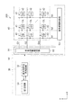
q+1本の元信号線(第0元信号線から第q元信号線)は其々実装領域20にて端子PADに接続する。一本の元信号線に対して一つの端子が形成されるので、端子PADの数はq+1個と非常に多くなる。そこで、実装領域20ではq+1個の端子PADをs行t列の行列状に配置する(sは2以上の整数、t=(q+1)/s)。本実施形態では、q+1=1028であるので、s=4、t=257として、端子PADを4行257列の行列状に配置している。例えば、第0元信号線は1行1列の端子PAD1−1に電気的に接続され、第1元信号線は1行2列の端子PAD1−2に電気的に接続され、以下同様にして、第1027元信号線は4行257列の端子PAD4−257に電気的に接続されている。尚、1行1列の端子PAD1−1から1行257列の端子PAD1−257迄が第1行目の端子PAD1である。同様に、2行1列の端子PAD2−1から2行257列の端子PAD2−257迄が第2行目の端子PAD2であり、3行1列の端子PAD3−1から3行257列の端子PAD3−257迄が第3行目の端子PAD3であり、4行1列の端子PAD4−1から4行257列の端子PAD4−257迄が第4行目の端子PAD4である。
The q + 1 original signal lines (from the 0th original signal line to the qth original signal line) are connected to the terminal PAD in the mounting
制御装置30と駆動回路51とは不図示のFPCを介して接続されている。FPCの接続部には接続領域が設けられており、接続領域には実装領域20に配置された端子PADと同じピッチで対応する接続端子が形成されている。FPCの接続端子と実装領域20の端子PADとは異方性導電フィルム(Anisotropic Conductive Film;ACF)や異方性導電ペースト(Anisotropic Conductive Paste;ACP)を用いて接続される。
The
尚、端子PADと配線とはアルミニウムや銅などの金属で形成され、これら金属は酸化珪素膜等の絶縁膜に覆われている。端子PADでは、FPCへの接触用に絶縁膜に開口部が設けられている。更に、端子PADの信頼性を増す為に、画素電極45を構成する導電材料(インジウム錫酸化物等)にて開口部を覆っていても良い。
Note that the terminal PAD and the wiring are formed of a metal such as aluminum or copper, and these metals are covered with an insulating film such as a silicon oxide film. In the terminal PAD, an opening is provided in the insulating film for contact with the FPC. Furthermore, in order to increase the reliability of the terminal PAD, the opening may be covered with a conductive material (indium tin oxide or the like) constituting the
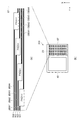
「配線形状」
図6は、実施形態1に係わる配線形状を説明する図で、(a)は一列分の端子に係わる配線形状を説明する図で、(b)は電気光学装置の構成を説明する概略平面図である。又、図7は、実施形態1に係わる配線形状を説明する図で、複数列分の端子に係わる配線形状を説明する図である。図8は、本発明の原理を説明する図である。図14は、比較例に係わる配線形状を説明する図で、(a)は一列分の端子に係わる配線形状を説明する図で、(b)は電気光学装置の構成を説明する概略平面図である。次に、図6乃至8と図14とを参照して、配線形状及び本発明の原理を説明する。尚、図14は従来技術に相当する比較例を説明する図であるが、説明を分かり易くする為に、本実施形態と同種類の構成には同じ符号や表記を用いている。
"Wiring shape"
6A and 6B are diagrams illustrating the wiring shape according to the first embodiment. FIG. 6A is a diagram illustrating the wiring shape related to one row of terminals. FIG. 6B is a schematic plan view illustrating the configuration of the electro-optical device. It is. FIG. 7 is a diagram illustrating the wiring shape according to the first embodiment, and is a diagram illustrating the wiring shape related to the terminals for a plurality of columns. FIG. 8 is a diagram for explaining the principle of the present invention. 14A and 14B are diagrams illustrating the wiring shape according to the comparative example. FIG. 14A is a diagram illustrating the wiring shape related to one row of terminals. FIG. 14B is a schematic plan view illustrating the configuration of the electro-optical device. is there. Next, the wiring shape and the principle of the present invention will be described with reference to FIGS. 6 to 8 and FIG. FIG. 14 is a diagram for explaining a comparative example corresponding to the prior art. In order to make the explanation easy to understand, the same reference numerals and notations are used for the same type of configuration as in the present embodiment.
図5は回路構成を説明する等価回路図であるので、電気光学装置200に於ける実際の配線形状はこれとは異なっている。まず、図6と図7とを参照して、実装領域20に於ける配線形状を説明する。
Since FIG. 5 is an equivalent circuit diagram for explaining the circuit configuration, the actual wiring shape in the electro-
図6(b)に示す様に、実装領域20は、素子基板62の表示領域40と素子基板62の外周の一辺67との間に配置されている。図6(a)は実装領域20の一部を拡大して描いたもので、具体的には実装領域20に於けるt列目の端子PAD(1行t列の端子PAD1−tから4行t列の端子PAD4−t迄の端子PAD)とそれに接続する配線とを説明している。図6(a)に示す様に、第1行目の端子PAD1は、表示領域40と素子基板62の外周の一辺67との間に配置され、第2行目の端子PAD2は、第1行目の端子PAD1と外周の一辺67との間に配置され、以下同様にして、第s行目の端子PADsは、第s−1行目の端子PADs−1と外周の一辺67との間に配置される。即ち、第1行目の端子PAD1が最も内側に位置して表示領域40に最も近く、第s行目の端子PADsが最も外側(素子基板62の外周の一辺67側)に位置して表示領域40から最も離れている。
As shown in FIG. 6B, the mounting
図6(a)に示す様に、実装領域20には、第1行目の端子PAD1に接続する第1の配線W1と、第2行目の端子PAD2に接続する第2の配線W2と、以下同様に第s行目の端子PADsに接続する第sの配線Wsとが形成されている。第1の配線W1は、表示領域40と外周の一辺67との間に延在している。即ち、第1の配線W1は、第1行目の端子PAD1から表示領域40に向かう第1のインバウンド配線IBW1と、第1行目の端子PAD1から素子基板62の外周の一辺67に向かう第1のアウトバウンド配線OBW1とを有している。第1のインバウンド配線IBW1は表示領域40と第1行目の端子PAD1の間に延在しており、第1のアウトバウンド配線OBW1は第1行目の端子PAD1と素子基板62の外周の一辺67との間に延在している。
As shown in FIG. 6A, the mounting
同様に、第2の配線W2は、表示領域40と外周の一辺67との間に延在している。即ち、第2の配線W2は、第2行目の端子PAD2から表示領域40に向かう第2のインバウンド配線IBW2と、第2行目の端子PAD2から素子基板62の外周の一辺67に向かう第2のアウトバウンド配線OBW2とを有している。第2のインバウンド配線IBW2は表示領域40と第2行目の端子PAD2の間に延在しており、第2のアウトバウンド配線OBW2は第2行目の端子PAD2と素子基板62の外周の一辺67との間に延在している。
Similarly, the second wiring W <b> 2 extends between the
以下同様にして、第sの配線Wsは、表示領域40と外周の一辺67との間に延在している。即ち、第sの配線Wsは、第s行目の端子PADsから表示領域40に向かう第sのインバウンド配線IBWsと、第s行目の端子PADsから素子基板62の外周の一辺67に向かう第sのアウトバウンド配線OBWsとを有している。第sのインバウンド配線IBWsは表示領域40と第s行目の端子PADsの間に延在しており、第sのアウトバウンド配線OBWsは第s行目の端子PADsと素子基板62の外周の一辺67との間に延在している。
Similarly, the sth wiring Ws extends between the
第1行目の端子PAD1は表示領域40に最も近い位置に配置されているので、第1のインバウンド配線IBW1はその他のインバウンド配線IBWよりも短い。反対に、第s行目の端子PADsは表示領域40から最も離れた位置に配置されているので、第sのインバウンド配線IBWsはその他のインバウンド配線IBWよりも長い。これに対して、第1行目の端子PAD1は表示領域40に最も近い位置に配置されているので、第1のアウトバウンド配線OBW1はその他のアウトバウンド配線OBWよりも長い。反対に、第s行目の端子PADsは表示領域40から最も離れた位置に配置されているので、第sのアウトバウンド配線OBWsはその他のアウトバウンド配線OBWよりも短い。この様に、インバウンド配線IBWの長さは第1行目の端子PAD1から第s行目の端子PADsへと行毎に長くなり、反対に、アウトバウンド配線OBWの長さは第1行目の端子PAD1から第s行目の端子PADsへと行毎に短くなる。この結果、第1の配線W1から第sの配線Ws迄、総ての配線の長さ(第1の配線W1の長さと第2の配線W2の長さと、と続き、第sの配線Wsの長さと)がほぼ等しくなっている。実際には、第1の配線W1から第sの配線Ws迄、総ての配線の長さがほぼ等しくなる様に第1のアウトバウンド配線OBW1から第sのアウトバウンド配線OBWs迄が配置される。
Since the terminal PAD1 in the first row is arranged at a position closest to the
各インバウンド配線IBWは、隣り合うインバウンド配線IBW間の距離がほぼ等しくなる様に配置される。具体的には、第1のインバウンド配線IBW1とその隣に位置する第2のインバウンド配線IBW2との距離と、第2のインバウンド配線IBW2とその隣に位置する第3のインバウンド配線IBW3との距離と、第3のインバウンド配線IBW3とその隣に位置する第4のインバウンド配線IBW4との距離と、第4のインバウンド配線IBW4とその隣に位置する第1のインバウンド配線IBW1との距離とは、ほぼ等しくなっている。 Each inbound wiring IBW is arranged so that the distance between adjacent inbound wirings IBW is substantially equal. Specifically, the distance between the first inbound wiring IBW1 and the second inbound wiring IBW2 located next thereto, and the distance between the second inbound wiring IBW2 and the third inbound wiring IBW3 located next thereto. The distance between the third inbound wiring IBW3 and the fourth inbound wiring IBW4 located next thereto is substantially equal to the distance between the fourth inbound wiring IBW4 and the first inbound wiring IBW1 located next thereto. It has become.
又、各アウトバウンド配線OBWは、隣り合うアウトバウンド配線OBW間の距離がほぼ等しくなる様に配置される。具体的には、第1のアウトバウンド配線OBW1とその隣に位置する第2のアウトバウンド配線OBW2との距離と、第2のアウトバウンド配線OBW2とその隣に位置する第3のアウトバウンド配線OBW3との距離と、第3のアウトバウンド配線OBW3とその隣に位置する第4のアウトバウンド配線OBW4との距離と、第4のアウトバウンド配線OBW4とその隣に位置する第1のアウトバウンド配線OBW1との距離とは、ほぼ等しくなっている。加えて、隣り合うインバウンド配線IBW間の距離と、隣り合うアウトバウンド配線OBW間の距離とは、ほぼ等しくなっている。 In addition, each outbound wiring OBW is arranged so that the distance between adjacent outbound wirings OBW is substantially equal. Specifically, the distance between the first outbound wiring OBW1 and the second outbound wiring OBW2 located next thereto, and the distance between the second outbound wiring OBW2 and the third outbound wiring OBW3 located next thereto. The distance between the third outbound wiring OBW3 and the fourth outbound wiring OBW4 located next thereto is substantially equal to the distance between the fourth outbound wiring OBW4 and the first outbound wiring OBW1 located next thereto. It has become. In addition, the distance between adjacent inbound wirings IBW and the distance between adjacent outbound wirings OBW are substantially equal.
インバウンド配線IBWは、実装領域20から信号線駆動回路53へと、隣り合うインバウンド配線IBW間の距離をほぼ等しく保った直線にて接続され、元信号線となる。具体的に数例を述べると、1行1列の端子PAD1−1のインバウンド配線IBW(1列目の第1のインバウンド配線IBW1)はそのまま第0元信号線となり、2行1列の端子PAD2−1のインバウンド配線IBW(1列目の第2のインバウンド配線IBW2)はそのまま第1元信号線となり、4行257列の端子PAD4−257のインバウンド配線IBW(257列目の第4のインバウンド配線IBW4)はそのまま第1027元信号線となる。又、アウトバウンド配線OBWは、以下に述べる寄生容量を揃える効果の他には回路上の機能はなく、所謂ダミー配線である。
The inbound wiring IBW is connected from the mounting
図7は、上述の構成とした際に、複数列分の端子とそれに係わる配線の形状を説明している。各配線の長さがほぼ等しく、隣り合う配線との間隔の関係も総ての配線で同等となっている。即ち、第1の配線W1と第2の配線W2と第3の配線W3と第4の配線W4とでは、総て配線長がほぼ等しく、且つ、隣り合う配線間の距離(配線間隔)もほぼ等しくなっている。 FIG. 7 illustrates the shape of the terminals for a plurality of columns and the wiring associated therewith when the above configuration is adopted. The lengths of the respective wirings are substantially equal, and the relationship between the distances between adjacent wirings is the same for all wirings. That is, the first wiring W1, the second wiring W2, the third wiring W3, and the fourth wiring W4 are all substantially the same in length, and the distance (wiring interval) between adjacent wirings is also substantially the same. Are equal.
図8は上述の構成がもたらす効果を定性的に説明した図で、総ての配線に関して、配線容量が同程度となっている事を表している。上述の構成とすると、具体的には、第1の配線W1が有する容量(第1配線容量)と第2の配線W2が有する容量(第2配線容量)と第3の配線W3が有する容量(第3配線容量)と第4の配線W4が有する容量(第4配線容量)とは同程度となる。図8に示す様に、例えば、第2の配線W2に関しては、上隣の第3の配線W3との間に上側寄生容量C1を有し、下隣の第1の配線W1との間に下側寄生容量C2を有し、これらの上側寄生容量C1と下側寄生容量C2とは、ほぼ等しくなる。上側寄生容量C1と下側寄生容量C2とが等しい関係は第1の配線W1に対しても、第2の配線W2に対しても、第3の配線W3に対しても、第4の配線W4に対しても、総ての配線に対して成り立つ。その結果、第1配線容量と第2配線容量と第3配線容量と第4配線容量とは(総ての配線容量は)ほぼ等しくなる。又、配線抵抗もほぼ等しくされているので、第1の配線W1に於ける信号伝達の時定数(第1配線の時定数)と第2の配線W2に於ける信号伝達の時定数(第2配線の時定数)と第3の配線W3に於ける信号伝達の時定数(第3配線の時定数)と第4の配線W4に於ける信号伝達の時定数(第4配線の時定数)とが、総て皆、同程度となる。この結果、第1配線の時定数と第2配線の時定数と第3配線の時定数と第4配線の時定数との相違に起因する表示ムラを抑制する事ができる。この様にして、表示ムラが抑制された高精細画像を表示する電気光学装置200を実現する事ができる。
FIG. 8 is a diagram qualitatively explaining the effects brought about by the above-described configuration, and shows that the wiring capacitance is the same for all wirings. Specifically, with the above configuration, the capacitance of the first wiring W1 (first wiring capacitance), the capacitance of the second wiring W2 (second wiring capacitance), and the capacitance of the third wiring W3 ( The third wiring capacity) and the capacity of the fourth wiring W4 (fourth wiring capacity) are approximately the same. As shown in FIG. 8, for example, the second wiring W2 has an upper parasitic capacitance C1 between the upper adjacent third wiring W3 and a lower adjacent first wiring W1. The upper parasitic capacitance C1 and the lower parasitic capacitance C2 are substantially equal. The upper parasitic capacitance C1 and the lower parasitic capacitance C2 are equal in relation to the first wiring W1, the second wiring W2, the third wiring W3, and the fourth wiring W4. This holds true for all wiring. As a result, the first wiring capacity, the second wiring capacity, the third wiring capacity, and the fourth wiring capacity are substantially equal (all wiring capacity). Also, since the wiring resistances are substantially equal, the time constant of signal transmission in the first wiring W1 (time constant of the first wiring) and the time constant of signal transmission in the second wiring W2 (second Wiring time constant), signal transmission time constant in the third wiring W3 (time constant of the third wiring), signal transmission time constant in the fourth wiring W4 (time constant of the fourth wiring), But all of them are on the same level. As a result, display unevenness due to the difference between the time constant of the first wiring, the time constant of the second wiring, the time constant of the third wiring, and the time constant of the fourth wiring can be suppressed. In this way, it is possible to realize the electro-
一般に、FPCの制約や端子PAD面積の確保等の理由により、端子PADの行間の距離が数mm程度に及び、例えば四行の実装であれば全体で10mm弱程度に及ぶ状況である。斯うした場合、図14に示される比較例では、各配線(元信号線)に付随する配線容量(隣接配線間容量等)に大きな差異が生じ、大きな配線容量差が生じ得る事となる。配線(元信号線)に配線容量差がある場合、その差異に起因して表示画像にムラが視認される場合があるが、本実施形態の構成は、この課題を確実に改善する事ができる。 Generally, the distance between the rows of the terminal PAD is about several millimeters, for example, due to restrictions of FPC and securing of the terminal PAD area. In such a case, in the comparative example shown in FIG. 14, a large difference occurs in the wiring capacitance (capacitance between adjacent wirings) associated with each wiring (original signal line), and a large wiring capacitance difference may occur. When there is a wiring capacity difference in the wiring (original signal line), unevenness may be visually recognized in the display image due to the difference, but the configuration of this embodiment can surely improve this problem. .
尚、厳密には、制御装置30の出力ピンから駆動回路51迄の時定数が総ての配線で揃う事が均一な画像表示を実現する。従って、FPCに於ける配線の時定数とインバウンド配線IBWの時定数との和が揃う必要がある。但し、FPCでの配線はパネルでの配線よりも十分に太くて低抵抗であり、FPCでの配線間の距離も大きいために配線間の寄生容量も小さく、FPCの配線での時定数は、インバウンド配線IBWの時定数に比較して非常に小さい。従って、電気光学装置200の端子PADで元信号を受ける際には、信号遅延にばらつきは殆ど問題にならない(非常に小さい)。図14に示される従来技術では、電気光学装置200での配線の配線容量が異なる為に、信号遅延にばらつきが発生し、表示ムラが現れる事もあった。これに対して、本実施形態では、第1配線の時定数も第2配線の時定数も第3配線の時定数も第4配線の時定数も皆同程度に揃う為、信号遅延に起因する表示ムラを抑制する事ができる。
Strictly speaking, the time constant from the output pin of the
又、本明細書にて「ほぼ等しい」とは、設計概念上等しい事を意味する。即ち、多少の誤差等が生じていても、設計概念で意図的に異ならせた他は「ほぼ等しい」と言える。 Further, in this specification, “substantially equal” means equal in terms of design concept. That is, even if some errors occur, it can be said that it is “substantially equal” except that it is intentionally different according to the design concept.
「他の電子機器」
電気光学装置200は上述の構成をなすが、この電気光学装置200を組み込んだ電子機器としては、図1を参照して説明したプロジェクターの他にも、リアプロジェクション型テレビ、直視型テレビ、携帯電話、携帯用オーディオ機器、パーソナルコンピューター、ビデオカメラのモニター、カーナビゲーション装置、ページャー、電子手帳、電卓、ワードプロセッサー、ワークステーション、テレビ電話、POS端末、ディジタルスチルカメラなどを挙げる事ができる。
"Other electronic devices"
The electro-
(実施形態2)
「配線形状が異なる形態1」
図9は、実施形態2に係わる配線形状を説明する図で、(a)は一列分の端子に係わる配線形状を説明する図で、(b)は電気光学装置の構成を説明する概略平面図である。又、図10は、実施形態2に係わる配線形状を説明する図で、複数列分の端子に係わる配線形状を説明する図である。次に、図9乃至10を参照して、実施形態2に係わる電気光学装置200を説明する。尚、実施形態1と同一の構成部位については、同一の符号を附し、重複する説明は省略する。
(Embodiment 2)
"
9A and 9B are diagrams illustrating the wiring shape according to the second embodiment. FIG. 9A is a diagram illustrating the wiring shape related to one row of terminals. FIG. 9B is a schematic plan view illustrating the configuration of the electro-optical device. It is. FIG. 10 is a diagram illustrating the wiring shape according to the second embodiment, and is a diagram illustrating the wiring shape related to terminals for a plurality of columns. Next, the electro-
図9に示す本実施形態の電気光学装置200は、図6に示された実施形態1の電気光学装置200と比べて、実装領域20に於ける配線形状が異なっている。それ以外の構成は、実施形態1とほぼ同様である。
The electro-
実施形態1の電気光学装置200(図6)では、配線が約90°曲がる屈曲部が見られた。これに対して、図9に示す様に、本実施形態の電気光学装置200は、端子PADに接続する総ての配線(第1の配線W1と、第2の配線W2と、と続き、第sの配線Wsと迄、本実施形態ではs=4)が、少なくとも実装領域20に於いては、直線である。更に、少なくとも実装領域20に於いては、各配線の長さ(インバウンド配線IBWの長さとアウトバウンド配線OBWの長さとの和)が等しくなっている。斯うした構成を為す結果、総ての配線(第1の配線W1と第2の配線W2と第3の配線W3と第4の配線W4)とで屈曲部が解消されているので、屈曲部に於ける信号反射の影響を回避する事ができる。この結果、配線に高速で信号を伝送する事ができる様になる。
In the electro-optical device 200 (FIG. 6) of the first embodiment, a bent portion where the wiring is bent by about 90 ° was observed. On the other hand, as shown in FIG. 9, the electro-
図7に示す実施形態1では、s行t列に配列された端子PADは、行方向の位置が揃うと共に列方向の位置も揃っていた。一方、図10に示す様に、本実施形態の電気光学装置200では、s行t列に配列された端子PADは、行方向(X軸に平行な方向で、インバウンド配線IBWの延在方向に直交する方向)では行毎に位置が揃っているものの(各行で端子PADのY座標がほぼ等しい)、列方向(Y軸に平行な方向で、インバウンド配線IBWの延在方向)の位置に関しては、行毎に一定のオフセット量を以てずれている(同じ列のs個の端子で端子PADのX座標が一定量ずつずれている)。例えば、同じ列に関して、2行目の端子PAD2は1行目の端子PAD1に対してX座標の値が所定量ずれており、3行目の端子PAD3は2行目の端子PAD2に対してX座標の値が先の所定量に同じ量ずれており、4行目の端子PAD4は3行目の端子PAD3に対してX座標の値が先の所定量に同じ量ずれており、その隣の列の1行目の端子PAD1は前の列のs行目の端子PADsに対してX座標の値が先の所定量に同じ量ずれている。この様に行毎に端子の列方向の座標が同じ量だけずれている。斯うする事で、端子PADに接続する総ての配線(第1の配線W1と、第2の配線W2と、と続き、第sの配線Wsと迄、本実施形態ではs=4)が、少なくとも実装領域20に於いては、直線となっている。なお実施形態2において、実装時のアライメントに使用するマーク(図示せず)のX座標を各実装端子行において同一にしておけば、FPCの貼り付け時における取り違い(所謂ポカミス)を回避することもできる。
In the first embodiment shown in FIG. 7, the terminals PAD arranged in the s rows and the t columns have the same position in the row direction and the same position in the column direction. On the other hand, as shown in FIG. 10, in the electro-
(実施形態3)
「配線形状が異なる形態2」
図11は、実施形態3に係わる配線形状を説明する図で、複数列分の端子に係わる配線形状を説明する図である。次に、図11を参照して、実施形態3に係わる電気光学装置200を説明する。尚、実施形態2と同一の構成部位については、同一の符号を附し、重複する説明は省略する。
(Embodiment 3)
"
FIG. 11 is a diagram illustrating the wiring shape according to the third embodiment, and is a diagram illustrating the wiring shape related to terminals for a plurality of columns. Next, an electro-
図11に示す本実施形態の電気光学装置200は、図10に示された実施形態2の電気光学装置200と比べて、実装領域20に於ける配線形状が異なっている。それ以外の構成は、実施形態2とほぼ同様である。
The electro-
実施形態2の電気光学装置200(図10)では、列方向に隣り合う端子PADの間が広がっていた。例えば、1行4列のPAD1−4と2行4列のPAD2−4との間には配線のない平面空間が広がっていた。この為に、この平面空間に於いては第1のアウトバウンド配線OBW1と第2のインバウンド配線IBW2との距離は、インバウンド配線IBW間の距離よりも大きくなっており、この部分では第1のアウトバウンド配線OBW1と第2のインバウンド配線IBW2との容量値が小さくなっていた。これに対して、本実施形態では、図11に示す様に、各インバウンド配線IBWの幅は、そのインバウンド配線IBWが接続する端子PADとの接続部に於いて、インバウンド配線IBWの幅の平均値よりも大きくなっている。例えば、1行4列のPAD1−4と2行4列のPAD2−4との間(図11にてDで示す部位)で、第2の配線W2の幅は、第2行目の端子PAD2との接続部に於いて、第2の配線W2の幅の平均値よりも大きくなっている。より具体的には、各インバウンド配線IBWの幅は、そのインバウンド配線IBWが接続する端子PADとの接続部に於いては、インバウンド配線IBWの幅(インバウンド配線IBWの行方向の長さ)と端子PADの幅(端子PADの行方向の長さ)とがほぼ一致している。斯うすると、総ての配線間距離がほぼ等しくなる。例えば、1行4列のPAD1−4と2行4列のPAD2−4との間(図11にてDで示す部位)にも太い第2の配線W2が形成されている。この為に、図11にてDで示す部位に於いても第1のアウトバウンド配線OBW1と第2のインバウンド配線IBW2との距離は、インバウンド配線IBW間の距離やアウトバウンド配線OBW間の距離にほぼ等しくなり、第1配線容量と第2配線容量とを同程度とする事ができる。即ち、端子PADに接続する総ての配線容量を同程度とする事ができる。更に、図11にてDで示す部位のインバウンド配線IBWが太くなり、インバウンド配線IBWの配線抵抗が下がるので、総ての配線に関して配線時定数(第1配線の時定数から第s配線の時定数)の増大を抑制する事ができる。 In the electro-optical device 200 (FIG. 10) of the second embodiment, the space between the terminals PAD adjacent in the column direction is widened. For example, a plane space without wiring has spread between the PAD1-4 of 1 row and 4 columns and the PAD2-4 of 2 rows and 4 columns. For this reason, in this plane space, the distance between the first outbound wiring OBW1 and the second inbound wiring IBW2 is larger than the distance between the inbound wiring IBW, and in this portion, the first outbound wiring The capacitance values of OBW1 and second inbound wiring IBW2 were small. On the other hand, in this embodiment, as shown in FIG. 11, the width of each inbound wiring IBW is the average value of the width of the inbound wiring IBW at the connection portion with the terminal PAD to which the inbound wiring IBW is connected. Is bigger than. For example, the width of the second wiring W2 between the PAD1-4 in the first row and the fourth column and the PAD2-4 in the second row and the fourth column (the portion indicated by D in FIG. 11) is the second row terminal PAD2. Is larger than the average width of the second wiring W2. More specifically, the width of each inbound wiring IBW is the width of the inbound wiring IBW (the length in the row direction of the inbound wiring IBW) and the terminal at the connection portion with the terminal PAD to which the inbound wiring IBW is connected. The width of the PAD (the length of the terminal PAD in the row direction) is almost the same. In this case, the distances between all the wires are almost equal. For example, the thick second wiring W2 is also formed between the PAD1-4 in the first row and the fourth column and the PAD2-4 in the second row and the fourth column (part indicated by D in FIG. 11). For this reason, even in the portion indicated by D in FIG. 11, the distance between the first outbound wiring OBW1 and the second inbound wiring IBW2 is substantially equal to the distance between the inbound wiring IBW and the distance between the outbound wiring OBW. Thus, the first wiring capacitance and the second wiring capacitance can be made comparable. That is, all the wiring capacities connected to the terminal PAD can be made the same level. Further, since the inbound wiring IBW at the portion indicated by D in FIG. 11 becomes thick and the wiring resistance of the inbound wiring IBW decreases, the wiring time constant (from the time constant of the first wiring to the time constant of the s-th wiring) for all wirings. ) Can be suppressed.
(実施形態4)
「接続関係が異なる形態」
図12は、実施形態4に係わる電気光学装置の回路構成と実装領域の構成とを説明した図である。次に、図12を参照して、実施形態4に係わる信号線駆動回路53及び実装領域20の構成を説明する。尚、実施形態1乃至3と同一の構成部位については、同一の符号を附し、重複する説明は省略する。
(Embodiment 4)
"Forms with different connection relationships"
FIG. 12 is a diagram illustrating a circuit configuration and a mounting area configuration of the electro-optical device according to the fourth embodiment. Next, the configuration of the signal
図12に示す本実施形態の電気光学装置200は、図5に示された実施形態1の電気光学装置200と比べて、端子PADと回路との配置関係が異なっている。それ以外の構成は、実施形態1とほぼ同様である。
The electro-
実施形態1乃至3(図5)では、信号線駆動回路53が薄膜素子にて素子基板62に形成されていた。これに対して、本実施例では、信号線駆動回路53は単結晶半導体基板に形成される半導体集積回路で構成されている。その為に、端子の数は画素41の列数nとなる。端子PADは実装領域20にてs行t列(st=n)に配列され、各端子PADからのインバウンド配線IBWは信号線43となる。本実施形態では、n=4112で、s=4、t=1028である。信号線駆動回路53と端子PADとは不図示のFPCを介して接続されている。
In the first to third embodiments (FIG. 5), the signal
実装領域20は表示領域40の外側で表示領域40に沿って形成され、表示領域40と外周の一辺67との間に配置される。各端子PADには信号線駆動回路53より、不図示のFPCを介して、プリチャージ信号や画像信号が供給され、プリチャージ信号や画像信号は、n本の信号線43に供給される。各端子PADに関して、インバウンド配線IBWとアウトバウンド配線OBWとの関係は実施形態1乃至3と同様である。
The mounting
本発明は上述した実施形態に限定されず、上述した実施形態に種々の変更や改良などを加えることが可能である。変形例を以下に説明する。 The present invention is not limited to the above-described embodiment, and various modifications and improvements can be added to the above-described embodiment. A modification will be described below.
(変形例1)
「アウトバウンド配線が異なる形態」
図13は、変形例1に係わる配線形状を説明する図で、(a)は一列分の端子に係わる配線形状を説明する図で、(b)は電気光学装置の構成を説明する概略平面図である。次に、図13を参照して、変形例1に係わる電気光学装置200を説明する。尚、実施形態1乃至4と同一の構成部位については、同一の符号を附し、重複する説明は省略する。
(Modification 1)
"Outbound wiring has different forms"
FIGS. 13A and 13B are diagrams illustrating the wiring shape according to the first modification. FIG. 13A is a diagram illustrating the wiring shape related to one row of terminals. FIG. 13B is a schematic plan view illustrating the configuration of the electro-optical device. It is. Next, an electro-
図13に示す本変形例の電気光学装置200は、図6に示された実施形態1の電気光学装置200と比べて、アウトバウンド配線OBWが異なっている。それ以外の構成は、実施形態1とほぼ同様である。
The electro-
実施形態1(図6)では、s行目端子PADsにも第sのアウトバウンド配線OBWsが配置されていた。これに対し、本変形例では、s行目の端子PADsにはアウトバウンド配線OBWが形成されていない。表示領域40から最も離れ、素子基板62の外周の一辺67に最も近い最終行(s行目)の端子PADsにはアウトバウンド配線OBWを形成しなくても良い。この場合も、少なくとも実装領域20に於いては、各端子に関し、インバウンド配線IBWの長さとアウトバウンド配線OBWの長さとの和が、等しくなる様にする。本変形例の様にs=4であれば、第1のインバウンド配線IBW1の長さと第1のアウトバウンド配線OBW1の長さとの和が、第2のインバウンド配線IBW2の長さと第2のアウトバウンド配線OBW2の長さとの和に等しく、更に、第3のインバウンド配線IBW3の長さと第3のアウトバウンド配線OBW3の長さとの和に等しく、更に、第4のインバウンド配線IBW4の長さに等しくする。斯うした構成としても、実施形態1乃至4と同じ効果が得られる。
In the first embodiment (FIG. 6), the sth outbound wiring OBWs is also arranged at the s-th row terminal PADs. On the other hand, in this modification, the outbound wiring OBW is not formed at the terminal PADs in the sth row. The outbound wiring OBW may not be formed at the terminal PADs in the last row (s-th row) that is farthest from the
(変形例2)
「アウトバンド配線の延在する終点が異なる形態」
これまでの実施例ではアウトバンド配線OBWについては外周の一辺67の手前(表示領域40側)を終点としているが、外周の一辺67に到達していてもよい。あるいは外周の一辺67を超えて延在させて形成し、その後の製造工程で外周の一辺67の位置で切断する過程を経てもよい。
(Modification 2)
“Outband wiring has different end points”
In the embodiments described so far, the outband wiring OBW has an end point in front of the one
Gi…i行目の走査線、IBW1…第1のインバウンド配線、IBW2…第2のインバウンド配線、IBW3…第3のインバウンド配線、IBW4…第4のインバウンド配線、OSj…第j元信号、OBW1…第1のアウトバウンド配線、OBW2…第2のアウトバウンド配線、OBW3…第3のアウトバウンド配線、OBW4…第4のアウトバウンド配線、PAD1…第1行目の端子、PAD2…第2行目の端子、PAD3…第3行目の端子、PAD4…第4行目の端子、SEL1…第1系列信号、SEL2…第2系列信号、SEL3…第3系列信号、SEL4…第4系列信号、Sjk+p…(jk+p)列目の信号線、SW1…第1スイッチ、SW2…第2スイッチ、SW3…第3スイッチ、SW4…第4スイッチ、W1…第1の配線、W2…第2の配線、W3…第3の配線、W4…第4の配線、20…実装領域、30…制御装置、32…表示用信号供給回路、33…記憶回路、40…表示領域、41…画素、42…走査線、43…信号線、44…画素トランジスター、45…画素電極、46…液晶、47…共通電極、48…遮光膜、50…駆動部、51…駆動回路、52…走査線駆動回路、53…信号線駆動回路、62…素子基板、63…対向基板、64…シール材、65…第1配向膜、66…第2配向膜、67…外周の一辺、200…電気光学装置、201…第一パネル、202…第二パネル、203…第三パネル、1000…投射型表示装置、1100…照明光学系、1300…投射光学系、1400…投射面。
Gi ... i-th scanning line, IBW1 ... first inbound wiring, IBW2 ... second inbound wiring, IBW3 ... third inbound wiring, IBW4 ... fourth inbound wiring, OSj ... j-th original signal, OBW1 ... 1st outbound wiring, OBW2 ... 2nd outbound wiring, OBW3 ... 3rd outbound wiring, OBW4 ... 4th outbound wiring, PAD1 ... 1st line terminal, PAD2 ... 2nd line terminal, PAD3 ... 3rd row terminal, PAD4 ... 4th row terminal, SEL1 ... 1st series signal, SEL2 ... 2nd series signal, SEL3 ... 3rd series signal, SEL4 ... 4th series signal, Sjk + p ... (jk + p) columns Eye signal line, SW1 ... first switch, SW2 ... second switch, SW3 ... third switch, SW4 ... fourth switch, W1 ... first wiring, DESCRIPTION OF
Claims (11)
前記素子基板には、第1行目の端子と、第2行目の端子と、前記第1行目の端子に接続する第1の配線と、前記第2行目の端子に接続する第2の配線とが形成されており、
前記第1行目の端子は、前記表示領域と前記素子基板の外周の一辺との間に配置され、
前記第2行目の端子は、前記第1行目の端子と前記外周の一辺との間に配置され、
前記第1の配線は、前記表示領域と前記外周の一辺との間に延在し、
前記第2の配線は、前記表示領域と前記第2行目の端子との間に延在する事を特徴とする電気光学装置。 Comprising an element substrate having a display area;
The element substrate includes a first row terminal, a second row terminal, a first wiring connected to the first row terminal, and a second row connected to the second row terminal. Of wiring and is formed,
The terminal in the first row is disposed between the display region and one side of the outer periphery of the element substrate,
The terminal of the second row is disposed between the terminal of the first row and one side of the outer periphery,
The first wiring extends between the display region and one side of the outer periphery,
The electro-optical device, wherein the second wiring extends between the display region and the second row terminal.
前記駆動回路は、前記表示領域と前記素子基板の外周の一辺との間に配置され、
前記素子基板には、第1行目の端子と、第2行目の端子と、前記第1行目の端子に接続する第1の配線と、前記第2行目の端子に接続する第2の配線とが形成されており、
前記第1行目の端子は、前記駆動回路と前記素子基板の外周の一辺との間に配置され、
前記第2行目の端子は、前記第1行目の端子と前記外周の一辺との間に配置され、
前記第1の配線は、前記駆動回路と前記外周の一辺との間に延在し、
前記第2の配線は、前記駆動回路と前記第2行目の端子との間に延在する事を特徴とする電気光学装置。 An element substrate having a display area and a drive circuit;
The drive circuit is disposed between the display region and one side of the outer periphery of the element substrate,
The element substrate includes a first row terminal, a second row terminal, a first wiring connected to the first row terminal, and a second row connected to the second row terminal. Of wiring and is formed,
The terminal of the first row is disposed between the drive circuit and one side of the outer periphery of the element substrate,
The terminal of the second row is disposed between the terminal of the first row and one side of the outer periphery,
The first wiring extends between the drive circuit and one side of the outer periphery,
The electro-optical device, wherein the second wiring extends between the driving circuit and a terminal of the second row.
Priority Applications (1)
| Application Number | Priority Date | Filing Date | Title |
|---|---|---|---|
| JP2013248933A JP2015106109A (en) | 2013-12-02 | 2013-12-02 | Electro-optic device and electronic equipment |
Applications Claiming Priority (1)
| Application Number | Priority Date | Filing Date | Title |
|---|---|---|---|
| JP2013248933A JP2015106109A (en) | 2013-12-02 | 2013-12-02 | Electro-optic device and electronic equipment |
Publications (2)
| Publication Number | Publication Date |
|---|---|
| JP2015106109A true JP2015106109A (en) | 2015-06-08 |
| JP2015106109A5 JP2015106109A5 (en) | 2016-12-28 |
Family
ID=53436239
Family Applications (1)
| Application Number | Title | Priority Date | Filing Date |
|---|---|---|---|
| JP2013248933A Pending JP2015106109A (en) | 2013-12-02 | 2013-12-02 | Electro-optic device and electronic equipment |
Country Status (1)
| Country | Link |
|---|---|
| JP (1) | JP2015106109A (en) |
Cited By (5)
| Publication number | Priority date | Publication date | Assignee | Title |
|---|---|---|---|---|
| US10032804B2 (en) | 2016-07-26 | 2018-07-24 | Seiko Epson Corporation | Electro-optic apparatus and electronic device |
| US10212832B2 (en) | 2017-02-06 | 2019-02-19 | Seiko Epson Corporation | Electro-optical panel, electro-optical device, and electronic apparatus |
| US10237968B2 (en) | 2017-02-06 | 2019-03-19 | Seiko Epson Corporation | Electrooptical apparatus and electronic device |
| US11528814B2 (en) | 2019-03-05 | 2022-12-13 | Seiko Epson Corporation | Electrooptical device and electronic apparatus |
| US11730028B2 (en) | 2020-07-31 | 2023-08-15 | Samsung Display Co., Ltd. | Display apparatus |
Citations (5)
| Publication number | Priority date | Publication date | Assignee | Title |
|---|---|---|---|---|
| JPS60107829U (en) * | 1983-12-20 | 1985-07-22 | セイコーエプソン株式会社 | LCD panel mounting structure |
| JP2005283830A (en) * | 2004-03-29 | 2005-10-13 | Seiko Epson Corp | Mounting structure, electrooptic device, electronic equipment, inspection method of mounting structure and inspection method of electrooptic device |
| JP2008083072A (en) * | 2005-01-07 | 2008-04-10 | Sharp Corp | Display device |
| JP2011008051A (en) * | 2009-06-26 | 2011-01-13 | Mitsubishi Electric Corp | Liquid crystal display device and inspection method for liquid crystal display device |
| JP2011164281A (en) * | 2010-02-08 | 2011-08-25 | Toshiba Mobile Display Co Ltd | Display device |
-
2013
- 2013-12-02 JP JP2013248933A patent/JP2015106109A/en active Pending
Patent Citations (5)
| Publication number | Priority date | Publication date | Assignee | Title |
|---|---|---|---|---|
| JPS60107829U (en) * | 1983-12-20 | 1985-07-22 | セイコーエプソン株式会社 | LCD panel mounting structure |
| JP2005283830A (en) * | 2004-03-29 | 2005-10-13 | Seiko Epson Corp | Mounting structure, electrooptic device, electronic equipment, inspection method of mounting structure and inspection method of electrooptic device |
| JP2008083072A (en) * | 2005-01-07 | 2008-04-10 | Sharp Corp | Display device |
| JP2011008051A (en) * | 2009-06-26 | 2011-01-13 | Mitsubishi Electric Corp | Liquid crystal display device and inspection method for liquid crystal display device |
| JP2011164281A (en) * | 2010-02-08 | 2011-08-25 | Toshiba Mobile Display Co Ltd | Display device |
Cited By (5)
| Publication number | Priority date | Publication date | Assignee | Title |
|---|---|---|---|---|
| US10032804B2 (en) | 2016-07-26 | 2018-07-24 | Seiko Epson Corporation | Electro-optic apparatus and electronic device |
| US10212832B2 (en) | 2017-02-06 | 2019-02-19 | Seiko Epson Corporation | Electro-optical panel, electro-optical device, and electronic apparatus |
| US10237968B2 (en) | 2017-02-06 | 2019-03-19 | Seiko Epson Corporation | Electrooptical apparatus and electronic device |
| US11528814B2 (en) | 2019-03-05 | 2022-12-13 | Seiko Epson Corporation | Electrooptical device and electronic apparatus |
| US11730028B2 (en) | 2020-07-31 | 2023-08-15 | Samsung Display Co., Ltd. | Display apparatus |
Similar Documents
| Publication | Publication Date | Title |
|---|---|---|
| US9875699B2 (en) | Display device | |
| JP5024110B2 (en) | Electro-optical device and electronic apparatus | |
| WO2018062023A1 (en) | Display panel | |
| KR101204365B1 (en) | Liquid crystal display panel and method of manufacturing the same | |
| JP5770796B2 (en) | Liquid crystal display device | |
| US10319316B2 (en) | Electro-optical device including a plurality of scanning lines | |
| JP4049162B2 (en) | Electro-optical device and electronic apparatus | |
| US9601041B2 (en) | Electro-optic device and electronic device | |
| WO2017022620A1 (en) | Active matrix substrate and display panel | |
| JP2015106109A (en) | Electro-optic device and electronic equipment | |
| JP6880623B2 (en) | Electro-optics and electronic equipment | |
| US20210225879A1 (en) | Circuit substrate and display device | |
| US20150338692A1 (en) | Display device | |
| KR20080002336A (en) | A liquid crystal display device | |
| JP4305485B2 (en) | Liquid crystal device, driving method of liquid crystal device, projector and electronic apparatus | |
| JP4345797B2 (en) | Liquid crystal device, projector and electronic device | |
| CN112014986B (en) | Circuit substrate and display panel | |
| JP5861740B2 (en) | Electro-optical device and electronic apparatus | |
| JP2018017811A (en) | Electro-optical device and electronic apparatus | |
| JP2004258365A (en) | Electrooptical device and electronic apparatus using it | |
| JP2021139937A (en) | Display device | |
| KR102262709B1 (en) | Flat panel display device | |
| JP5678992B2 (en) | Electro-optical device and electronic apparatus | |
| JP4913991B2 (en) | Mounting structure, electro-optical device, and electronic apparatus | |
| JP2008040290A (en) | Electrooptical device and electronic equipment |
Legal Events
| Date | Code | Title | Description |
|---|---|---|---|
| RD04 | Notification of resignation of power of attorney |
Free format text: JAPANESE INTERMEDIATE CODE: A7424 Effective date: 20160617 |
|
| RD03 | Notification of appointment of power of attorney |
Free format text: JAPANESE INTERMEDIATE CODE: A7423 Effective date: 20160627 |
|
| A521 | Request for written amendment filed |
Free format text: JAPANESE INTERMEDIATE CODE: A523 Effective date: 20161115 |
|
| A621 | Written request for application examination |
Free format text: JAPANESE INTERMEDIATE CODE: A621 Effective date: 20161115 |
|
| A977 | Report on retrieval |
Free format text: JAPANESE INTERMEDIATE CODE: A971007 Effective date: 20170830 |
|
| A131 | Notification of reasons for refusal |
Free format text: JAPANESE INTERMEDIATE CODE: A131 Effective date: 20170905 |
|
| A521 | Request for written amendment filed |
Free format text: JAPANESE INTERMEDIATE CODE: A523 Effective date: 20171030 |
|
| A02 | Decision of refusal |
Free format text: JAPANESE INTERMEDIATE CODE: A02 Effective date: 20180306 |