JP2015049123A - Detector module manufacturing method, detector module and medical image diagnostic device - Google Patents
Detector module manufacturing method, detector module and medical image diagnostic device Download PDFInfo
- Publication number
- JP2015049123A JP2015049123A JP2013180650A JP2013180650A JP2015049123A JP 2015049123 A JP2015049123 A JP 2015049123A JP 2013180650 A JP2013180650 A JP 2013180650A JP 2013180650 A JP2013180650 A JP 2013180650A JP 2015049123 A JP2015049123 A JP 2015049123A
- Authority
- JP
- Japan
- Prior art keywords
- detector module
- array
- scintillator
- manufacturing
- detector
- Prior art date
- Legal status (The legal status is an assumption and is not a legal conclusion. Google has not performed a legal analysis and makes no representation as to the accuracy of the status listed.)
- Abandoned
Links
- 238000004519 manufacturing process Methods 0.000 title claims abstract description 69
- 239000000853 adhesive Substances 0.000 claims abstract description 110
- 230000001070 adhesive effect Effects 0.000 claims abstract description 107
- 239000000463 material Substances 0.000 claims abstract description 21
- 238000000034 method Methods 0.000 abstract description 41
- 238000010586 diagram Methods 0.000 description 26
- 238000002591 computed tomography Methods 0.000 description 24
- 238000001514 detection method Methods 0.000 description 14
- 238000012545 processing Methods 0.000 description 12
- 239000000758 substrate Substances 0.000 description 9
- 239000012790 adhesive layer Substances 0.000 description 8
- 238000012937 correction Methods 0.000 description 5
- 238000007781 pre-processing Methods 0.000 description 5
- 238000007796 conventional method Methods 0.000 description 4
- 238000009826 distribution Methods 0.000 description 4
- 239000007788 liquid Substances 0.000 description 4
- 238000012986 modification Methods 0.000 description 4
- 230000004048 modification Effects 0.000 description 4
- 229920000298 Cellophane Polymers 0.000 description 3
- 238000003491 array Methods 0.000 description 3
- 238000013500 data storage Methods 0.000 description 3
- 238000003860 storage Methods 0.000 description 3
- 230000001629 suppression Effects 0.000 description 3
- 238000006243 chemical reaction Methods 0.000 description 2
- 238000010191 image analysis Methods 0.000 description 2
- 238000003384 imaging method Methods 0.000 description 2
- 238000002347 injection Methods 0.000 description 2
- 239000007924 injection Substances 0.000 description 2
- 238000005304 joining Methods 0.000 description 2
- 230000035945 sensitivity Effects 0.000 description 2
- 230000003321 amplification Effects 0.000 description 1
- 239000000919 ceramic Substances 0.000 description 1
- 230000006835 compression Effects 0.000 description 1
- 238000007906 compression Methods 0.000 description 1
- 238000013480 data collection Methods 0.000 description 1
- 230000002950 deficient Effects 0.000 description 1
- 239000000284 extract Substances 0.000 description 1
- 239000003292 glue Substances 0.000 description 1
- 238000009434 installation Methods 0.000 description 1
- 239000010410 layer Substances 0.000 description 1
- 238000009206 nuclear medicine Methods 0.000 description 1
- 238000003199 nucleic acid amplification method Methods 0.000 description 1
- 230000003287 optical effect Effects 0.000 description 1
- 239000003973 paint Substances 0.000 description 1
- 238000005498 polishing Methods 0.000 description 1
- 230000005855 radiation Effects 0.000 description 1
- 238000009877 rendering Methods 0.000 description 1
- 239000007787 solid Substances 0.000 description 1
- 238000009281 ultraviolet germicidal irradiation Methods 0.000 description 1
- 230000000007 visual effect Effects 0.000 description 1
Images


Abstract
Description
本発明の実施形態は、検出器モジュール製造方法、検出器モジュール及び医用画像診断装置に関する。 Embodiments described herein relate generally to a detector module manufacturing method, a detector module, and a medical image diagnostic apparatus.
従来、固体検出器は、被検体を透過したX線の強度を電気信号に変換する検出器として、多くのX線コンピュータ断層撮影(CT:Computed Tomography)装置に搭載されている。固体検出器は、X線の入射によりシンチレータ(scintillator)が発光したシンチレータ光をフォトダイオード(photodiode)により光電変換する検出器であり、複数の検出器モジュールにより構成される。 Conventionally, solid-state detectors are mounted on many X-ray computed tomography (CT) apparatuses as detectors that convert the intensity of X-rays that have passed through a subject into electrical signals. The solid state detector is a detector that photoelectrically converts scintillator light emitted from a scintillator by the incidence of X-rays by a photodiode, and is configured by a plurality of detector modules.
かかる検出器モジュールは、シンチレータアレイ(scintillator array)とフォトダイオードアレイ(photodiode array)とを光学的に接合することで製造される。一般的には、検出器モジュールは、シンチレータアレイとフォトダイオードアレイとを、UV(ultraviolet)硬化型接着剤等の液状接着剤で接着することで製造される。 Such a detector module is manufactured by optically joining a scintillator array and a photodiode array. In general, a detector module is manufactured by bonding a scintillator array and a photodiode array with a liquid adhesive such as an ultraviolet (UV) curable adhesive.
しかし、接着剤で形成される接着層は、シンチレータアレイの反り等により、不均一となる場合がある。また、かかる製造方法は、接着剤を用いることにより、複雑な製造工程が必要となる。このため、かかる製造方法は、例えば、設備の機械障害による長時間の製造工程の停止(ドカ停)が発生したり、ランニングコストが増大したりする場合があった。このように、接着剤を用いた従来の製造方法は、歩留まりが低くなる場合がある。 However, the adhesive layer formed of the adhesive may become non-uniform due to warpage of the scintillator array or the like. Moreover, this manufacturing method requires a complicated manufacturing process by using an adhesive. For this reason, in such a manufacturing method, for example, the manufacturing process may be stopped for a long time due to a mechanical failure of the facility (doker stop), or the running cost may increase. Thus, the conventional manufacturing method using an adhesive may have a low yield.
本発明が解決しようとする課題は、歩留まりを向上することができる検出器モジュール製造方法、検出器モジュール及び医用画像診断装置を提供することである。 The problem to be solved by the present invention is to provide a detector module manufacturing method, a detector module, and a medical image diagnostic apparatus capable of improving the yield.
実施形態の検出器モジュール製造方法は、検出器モジュールを製造する方法である。検出器モジュールは、X線により発光するシンチレータアレイと、前記シンチレータアレイが発生した光を電気信号に変換するフォトダイオードアレイとが光学的に接合される。実施形態の検出器モジュール製造方法は、両面に接着面を有する透明接着シートの一方の接着面と、前記フォトダイオードアレイとを接着する。そして、前記フォトダイオードアレイが若干の柔軟性を有する材質で構成される場合、前記透明接着シートの他方の接着面を、前記フォトダイオードアレイの反りにより突出させた状態で、前記シンチレータアレイに接着する。 The detector module manufacturing method of the embodiment is a method of manufacturing a detector module. In the detector module, a scintillator array that emits light by X-rays and a photodiode array that converts light generated by the scintillator array into an electrical signal are optically joined. In the detector module manufacturing method of the embodiment, one of the adhesive surfaces of a transparent adhesive sheet having adhesive surfaces on both sides is bonded to the photodiode array. When the photodiode array is made of a material having some flexibility, the other adhesive surface of the transparent adhesive sheet is bonded to the scintillator array in a state where the other adhesive surface protrudes due to warpage of the photodiode array. .
以下、添付図面を参照して、検出器モジュール製造方法の実施形態を詳細に説明する。以下の実施形態で製造される検出器モジュールは、シンチレータアレイとフォトダイオードアレイとが光学的に接合される。シンチレータアレイは、X線により発光し、フォトダイオードアレイは、シンチレータアレイが発生した光を電気信号に変換する。 Hereinafter, an embodiment of a detector module manufacturing method will be described in detail with reference to the accompanying drawings. In the detector module manufactured in the following embodiment, a scintillator array and a photodiode array are optically bonded. The scintillator array emits light by X-rays, and the photodiode array converts light generated by the scintillator array into an electrical signal.
以下では、検出器モジュール製造方法により製造される検出器モジュールが搭載される医用画像診断装置が、X線コンピュータ断層撮影(CT:Computed Tomography)装置である場合を一例として説明する。 Hereinafter, a case where the medical image diagnostic apparatus on which the detector module manufactured by the detector module manufacturing method is mounted is an X-ray computed tomography (CT) apparatus will be described as an example.
(実施形態)
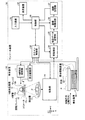
まず、本実施形態に係る検出器モジュール製造方法により製造される検出器モジュールが搭載されるX線CT装置の構成について説明する。図1は、本実施形態に係るX線CT装置の構成例を示す図である。図1に示すように、本実施形態に係るX線CT装置は、架台装置10と、寝台装置20と、コンソール装置30とを有する。
(Embodiment)
First, the configuration of an X-ray CT apparatus on which a detector module manufactured by the detector module manufacturing method according to the present embodiment is mounted will be described. FIG. 1 is a diagram illustrating a configuration example of an X-ray CT apparatus according to the present embodiment. As shown in FIG. 1, the X-ray CT apparatus according to the present embodiment includes a
架台装置10は、被検体PにX線を照射し、被検体Pを透過したX線の検出データから投影データを収集する装置であり、X線照射制御部11と、X線発生装置12と、検出器13と、収集部14と、回転フレーム15と、架台駆動部16とを有する。
The
回転フレーム15は、後述するX線管12aを有するX線発生装置12と検出器13とを被検体Pの周囲で回転可能に支持する。回転フレーム15は、X線発生装置12と検出器13とを被検体Pを挟んで対向支持し、後述する架台駆動部16によって被検体Pを中心とした円軌道にて高速に回転する円環状のフレームである。
The rotating
X線発生装置12は、X線を発生し、発生したX線を被検体Pへ照射する装置であり、X線管12aと、ウェッジ12bと、コリメータ12cとを有する。
The X-ray generator 12 is an apparatus that generates X-rays and irradiates the subject P with the generated X-rays, and includes an
X線管12aは、X線を曝射する。具体的には、X線管12aは、後述するX線照射制御部11により供給される高電圧により被検体PにX線ビームを発生する真空管である。X線管12aは、回転フレーム15の回転にともない、X線ビームを被検体Pに対して曝射する。X線管12aは、ファン角及びコーン角を持って広がるX線ビームを発生する。
The
ウェッジ12bは、X線管12aから曝射されたX線のX線量を調節するためのX線フィルタである。コリメータ12cは、後述するX線照射制御部11の制御により、ウェッジ12bによってX線量が調節されたX線の照射範囲を絞り込むためのスリットである。
The
X線照射制御部11は、高電圧発生部として、X線管12aに高電圧を供給する装置であり、X線管12aは、X線照射制御部11から供給される高電圧を用いてX線を発生する。X線照射制御部11は、X線管12aに供給する管電圧や管電流を調整することで、被検体Pに対して照射されるX線量を調整する。また、X線照射制御部11は、コリメータ12cの開口度を調整することにより、X線の照射範囲(ファン角やコーン角)を調整する。
The X-ray irradiation control unit 11 is a device that supplies a high voltage to the
架台駆動部16は、回転フレーム15を回転駆動させることによって、被検体Pを中心とした円軌道上でX線発生装置12と検出器13とを旋回させる。
The gantry driving unit 16 rotates the
検出器13は、X線管12aから曝射され被検体Pを透過したX線を検出する。具体的には、検出器13は、2次元状に配列された検出素子により、X線管12aから曝射されて被検体Pを透過したX線を検出する。図1に示す検出器13は、被検体Pを透過したX線の強度分布を示すX線強度分布データを出力する2次元アレイ型検出器(面検出器)である。検出器13には、チャンネル方向(図1に示すY軸方向)に配列された複数の検出素子(検出素子列)が、被検体Pの体軸方向(図1に示すZ軸方向)に沿って複数列配列される。体軸方向は、スライス方向とも呼ばれる。例えば、検出器13は、被検体Pの体軸方向に沿って320列に配列された検出素子列を有し、被検体Pを透過したX線強度分布データを広範囲に検出する。
The
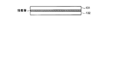
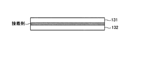
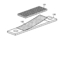
図2A及び図2Bは、図1に示す検出器の構成例を示す図である。図2Aに例示するように、検出器13は、検出器モジュール130が複数配列された構成となる。図2Aに例示する検出器13は、検出器モジュール130が、チャンネル方向(図1中のY軸方向)にN列、体軸方向(図1中のZ軸方向)にM列配置された面検出器である。また、検出器モジュール130は、図2Bに例示するように、シンチレータアレイ131とフォトダイオードアレイ132とが接着層を介して光学的に接合される。
2A and 2B are diagrams showing a configuration example of the detector shown in FIG. As illustrated in FIG. 2A, the
シンチレータアレイ131は、反射材により複数の区画に分割されている。その結果、シンチレータアレイ131は、複数のシンチレータがチャンネル方向及び体軸方向に格子状に高密度で配列された構成となる。各区画のシンチレータは、入射したX線のエネルギーに応じた光量の光(シンチレータ光)を発生する。
The
フォトダイオードアレイ132は、複数のフォトダイオードがチャンネル方向及び体軸方向に格子状に高密度で基板上に配列されている。フォトダイオードアレイ132は、基板上に作成され基台に取り付けられる。各フォトダイオードは、受光した光のエネルギーに応じた電気信号を出力する。シンチレータアレイ131の各区画(各シンチレータ)と、フォトダイオードアレイ132の各フォトダイオードとは、対向する位置に配列される。これにより、対向する位置に配列されたシンチレータとフォトダイオードとは、光学的に接合され、1つの検出素子を形成する。上記の反射材は、シンチレータ光を遮光し、且つ、反射する材質により形成され、個々のシンチレータが発生した光が、対向する位置のフォトダイオードで効率的に受光されるために形成される。
In the
ここで、シンチレータアレイ131の製造方法の一例について、図3A〜Dを用いて説明する。図3A〜Dは、シンチレータアレイの製造方法の一例を示す図である。まず、図3Aに例示するように、シンチレータ部材が直方体状のブロックに切り出されたシンチレータブロックと反射材とが交互にチャンネル方向に複数配列される。シンチレータブロックと反射材とは、接着剤により固定される。
Here, an example of a method for manufacturing the
そして、図3Bに示すように、図3Aの製造工程で製造された製造物に、チャンネル方向に平行な溝が、体軸方向に沿って複数形成される。そして、図3Cに示すように、図3Bの製造工程で形成された溝に、反射材が挿入される。例えば、図3Cでは、図3Bの製造工程で形成された溝に接着剤が注入された後に、反射材が挿入される。以下、図3Cの製造工程で製造された製造物を、シンチレータブロック1311と記載する。
And as shown to FIG. 3B, the groove | channel parallel to a channel direction is formed in the product manufactured by the manufacturing process of FIG. 3A along the body-axis direction. And as shown to FIG. 3C, a reflecting material is inserted in the groove | channel formed in the manufacturing process of FIG. 3B. For example, in FIG. 3C, after the adhesive is injected into the groove formed in the manufacturing process of FIG. 3B, the reflective material is inserted. Hereinafter, the product manufactured in the manufacturing process of FIG. 3C is referred to as a
そして、シンチレータブロック1311で溝が切り込まれた面は、研磨される。更に、シンチレータブロック1311で溝が切り込まれた面と反対側の面は、反射材が露出するように研磨加工により切り落とされる。これにより、図3Dに示すシンチレータアレイ131が製造される。なお、シンチレータアレイ131のX線入射面には、最終的に、白色ペイント等により反射層(表面リフレクター)が形成される。図3に例示する製造方法により製造されたシンチレータアレイ131には、反りが発生する場合がある。具体的には、反射材を接着剤により各区画のシンチレータと接着したことにより、シンチレータアレイ131には、溝が切り込まれた面と反対側の面(切り落とし面)が突出する反りが発生する場合がある。
Then, the surface where the groove is cut by the
なお、シンチレータアレイ131の製造方法は、図3A〜Dに例示する製造方法に限定されるものではない。例えば、反射材は、接着剤を用いる必要のない、液状反射材が用いられる場合であっても良い。また、シンチレータアレイ131は、平板状のシンチレータ部材に格子状の溝を形成し、この格子状の溝に液状反射材を注入することで製造される場合であっても良い。
Note that the manufacturing method of the
図1に戻って、収集部14は、DAS(data acquisition system)であり、検出器13が検出したX線の検出データを収集して、投影データを生成する。例えば、収集部14は、検出器13により検出されたX線強度分布データに対して、増幅処理やA/D変換処理等を行なって投影データを生成し、生成した投影データを後述するコンソール装置30に送信する。
Returning to FIG. 1, the
寝台装置20は、被検体Pを載せる装置であり、天板22と、寝台駆動装置21とを有する。天板22は、被検体Pが載置される板である。寝台駆動装置21は、後述するスキャン制御部33の制御のもと、天板22をZ軸方向へ移動することにより、被検体Pを回転フレーム15内(撮影空間内)に移動させる。
The
架台装置10は、例えば、天板22を移動させながら回転フレーム15を回転させて被検体Pをらせん状にスキャンするヘリカルスキャンを実行する。又は、架台装置10は、天板22を移動させた後に被検体Pの位置を固定したままで回転フレーム15を回転させて被検体Pを円軌道にてスキャンするコンベンショナルスキャンを実行する。又は、架台装置10は、天板22の位置を一定間隔で移動させてコンベンショナルスキャンを複数のスキャンエリアで行なうステップアンドシュート方式を実行する。
For example, the
コンソール装置30は、操作者によるX線CT装置の操作を受け付けるとともに、検出器13が出力したデータを用いてX線CT画像データを生成する装置である。すなわち、コンソール装置30は、架台装置10によって収集された投影データからX線CT画像データを再構成する装置であり、入力装置31と、表示装置32と、スキャン制御部33と、前処理部34と、投影データ記憶部35と、画像再構成部36と、画像記憶部37と、制御部38とを有する。
The
入力装置31は、X線CT装置の操作者が各種指示や各種設定の入力に用いるマウスやキーボード、ボタン、ペダル(フットスイッチ)等を有し、操作者から受け付けた指示や設定の情報を、制御部38に転送する。
The input device 31 includes a mouse, a keyboard, buttons, pedals (foot switches), etc., used by an operator of the X-ray CT apparatus for inputting various instructions and various settings, and receives instructions and setting information received from the operator. The data is transferred to the
表示装置32は、操作者が参照するモニタであり、制御部38による制御のもと、X線CT画像データを操作者に表示したり、入力装置31を介して操作者から各種指示や各種設定等を受け付けるためのGUI(Graphical User Interface)を表示したりする。
The
スキャン制御部33は、後述する制御部38の制御のもと、X線照射制御部11、架台駆動部16、収集部14及び寝台駆動装置21の動作を制御することで、架台装置10における投影データの収集処理を制御する。
The
前処理部34は、収集部14によって生成された投影データに対して、チャンネル間の感度補正処理と、対数変換処理と、オフセット補正、感度補正及びビームハードニング補正等の補正処理とを行なって、補正済みの投影データを生成する。以下では、前処理部34が生成する補正済みの投影データを再構成用投影データと記載する。
The preprocessing unit 34 performs sensitivity correction processing between channels, logarithmic conversion processing, correction processing such as offset correction, sensitivity correction, and beam hardening correction on the projection data generated by the
投影データ記憶部35は、前処理部34により生成された再構成用投影データを記憶する。画像再構成部36は、投影データ記憶部35が記憶する再構成用投影データを用いてX線CT画像データを再構成する。再構成方法としては、種々の方法があり、例えば、逆投影処理が挙げられる。また、逆投影処理としては、例えば、FBP(Filtered Back Projection)法による逆投影処理が挙げられる。或いは、画像再構成部36は、逐次近似法を用いて、X線CT画像データを再構成しても良い。
The projection
また、画像再構成部36は、ヘリカルスキャンや、面検出器である検出器13を用いたコンベンショナルスキャン、ステップアンドシュート方式のコンベンショナルスキャンにより収集された投影データを用いて、3次元X線CT画像データを再構成することができる。例えば、画像再構成部36は、複数のアキシャル面の断層像データとして3次元X線CT画像データを再構成する。また、画像再構成部36は、3次元X線CT画像データから、各種レンダリング処理を行なって、表示用の2次元画像データを生成する。画像記憶部37は、画像再構成部36が生成した各種画像データを記憶する。
In addition, the
制御部38は、架台装置10、寝台装置20及びコンソール装置30の動作を制御することによって、X線CT装置の全体制御を行う。具体的には、制御部38は、スキャン制御部33を制御することで、架台装置10で行なわれるスキャンを制御する。また、制御部38は、前処理部34や、画像再構成部36を制御することで、コンソール装置30における画像再構成処理や画像生成処理を制御する。また、制御部38は、画像記憶部37が記憶する各種画像データを、表示装置32に表示するように制御する。
The
以上、本実施形態に係るX線CT装置の全体構成について説明した。かかる構成のもと、本実施形態に係るX線CT装置は、検出器13が検出したデータを用いてX線CT画像データを生成する。ここで、上述したように、検出器13は、複数の検出器モジュール130から構成され、各検出器モジュール130は、シンチレータアレイ131とフォトダイオードアレイ132とを光学的に接合することで製造される。図4は、従来の検出器モジュール製造方法の一例を示す図である。
The overall configuration of the X-ray CT apparatus according to the present embodiment has been described above. Under such a configuration, the X-ray CT apparatus according to the present embodiment generates X-ray CT image data using data detected by the
従来の検出器モジュール製造方法では、図4に示すように、シンチレータアレイ131とフォトダイオードアレイ132とは、接着剤により接着される。かかる接着剤は、例えば、UV(ultraviolet)硬化型接着剤等の液状接着剤である。
In the conventional detector module manufacturing method, as shown in FIG. 4, the
しかし、接着剤で形成される接着層は、シンチレータアレイ131の反り等により、不均一となる場合がある。また、かかる製造方法は、接着剤を用いることにより、複雑な製造工程が必要となる。例えば、接着剤を用いる場合、接着前のシンチレータアレイ131とフォトダイオードアレイ132との間の距離(アレイ間距離)を一定の範囲にするための位置決め工程や、一定の範囲に位置決めされたアレイ間距離を保持する工程が必要となる。また、接着剤を用いる場合、例えば、接着剤の仮硬化及び本硬化を行なう工程や、余剰接着剤を除去する工程が必要となる。
However, the adhesive layer formed of an adhesive may become non-uniform due to warpage of the
このため、従来の製造方法は、例えば、設備の機械障害による長時間の製造工程の停止(ドカ停)が発生したり、ランニングコストが増大したりする場合があった。このように、従来の製造方法は、歩留まりが低くなる場合がある。 For this reason, in the conventional manufacturing method, for example, the manufacturing process may be stopped for a long time due to a mechanical failure of the facility (doker stop), or the running cost may increase. Thus, the conventional manufacturing method may have a low yield.
そこで、本実施形態に係る検出器モジュール130は、歩留まりを向上するために、以下の製造方法により製造される。図5は、本実施形態に係る検出器モジュール製造方法の概要を示す図である。本実施形態に係る検出器モジュール製造方法では、図5に示すように、シンチレータアレイ131とフォトダイオードアレイ132とを、両面に接着面を有する透明接着シート133により接着する。具体的には、透明接着シート133は、テープ式接着剤であり、例えば、OCA(Optical Clear Adhesive)である。
Therefore, the
本実施形態では、透明接着シート133を接着層とすることで、接着剤を用いる従来方法と比較して、シンチレータアレイ131とフォトダイオードアレイ132との間の距離を、透明接着シート133の厚みにより容易にコントロールできる。換言すると、本実施形態では、検出性能上、好適な厚みを有する透明接着シート133を製造又は購入するだけで、シンチレータアレイ131とフォトダイオードアレイ132との間の距離をコントロールすることができる。
In this embodiment, by using the transparent
例えば、本実施形態では、透明接着シート133の厚みは、シンチレータアレイ131とフォトダイオードアレイ132との間の距離が、検出器13の性能上、最適な所定の範囲内となる厚みとされる。具体的には、本実施形態では、透明接着シート133の厚みは、反射材により複数の区画に分割されたシンチレータアレイ131の各区画のシンチレータが発生した光の略全てが、フォトダイオードアレイ132において対向する位置のフォトダイオードに入射する厚みとされる。接着層が厚い場合、シンチレータが発生した光が対向する位置のフォトダイオードとは別のフォトダイオードにて受光される可能性がある。本実施形態では、かかる可能性が略無い厚みの透明接着シート133を用いることで、検出器モジュール130の検出特性を安定化することができる。
For example, in the present embodiment, the thickness of the transparent
また、図3A〜Dに例示した製造方法によりシンチレータアレイ131に反りが発生している場合、個々の検出器モジュール130の検出特性にばらつきが生じ、画質が低下する。また、シンチレータアレイ131に反りが発生している場合、散乱線の発生によりアーチファクトが発生し、画質が低下する。しかし、本実施形態では、透明接着シート133でシンチレータアレイ131とフォトダイオードアレイ132とを接着することで、シンチレータアレイ131の反りを、ある程度矯正することができ、個々の検出器モジュール130の検出特性が均一となり、更に、散乱線の発生が軽減して、画質を向上させることができる。また、本実施形態に係る製造方法は、透明接着シート133を貼るという簡易な方法であるため、設備や工程も簡素化でき、コストを削減することができる。このようなことから、本実施形態では、検出器モジュール130の製造における歩留まりが向上する。
Further, when the
以下、本実施形態に係る検出器モジュール製造方法の具体例について説明する。本製造方法は、第1工程と第2工程との2つの工程に大別される。本実施形態に係る第1工程では、フォトダイオードアレイ132と透明接着シート133の一方の接着面とが接着される。本実施形態に係る第2工程では、シンチレータアレイ131と透明接着シート133の他方の接着面とが接着される。
Hereinafter, a specific example of the detector module manufacturing method according to the present embodiment will be described. This manufacturing method is roughly divided into two steps, a first step and a second step. In the first step according to this embodiment, the
まず、透明接着シート133について、図6を用いて説明する。図6は、図5に示す透明接着シートを説明するための図である。透明接着シート133は、図6に示すように、両面の接着面が剥離シート133a及び剥離シート133bにより保護されている。剥離シート133aが剥離されることで、透明接着シート133の一方の接着面が露出し、剥離シート133bが剥離されることで、透明接着シート133の他方の接着面が露出する。剥離シート133a及び剥離シート133bは、例えば、セロハンテープを用いて手動で容易に剥がすことができる。透明接着シート133は、「剥離シート133a及び剥離シート133bで両面の接着層が保護された状態」、「剥離シート133aが剥がされて一方の接着面が露出し、他方の接着面が剥離シート133bで保護された状態」、「剥離シート133bが剥がされて一方の接着面が露出し、他方の接着面が剥離シート133aで保護された状態」及び「剥離シート133a及び剥離シート133bが剥がされて両面の接着層が露出した状態」のいずれかの状態となる。
First, the transparent
次に、第1工程について、図7A及びBを用いて説明する。図7A及びBは、第1工程を説明するための図である。 Next, the first step will be described with reference to FIGS. 7A and 7B. 7A and 7B are diagrams for explaining the first step.
第1工程では、フォトダイオードアレイ132と、透明接着シート133の一方の接着面とが接着される。例えば、第1工程では、作業者は、図7Aに示すように、セロハンテープを剥離シート133aの端部に貼り、セロハンテープを持ち上げることで、剥離シート133aを剥がす。そして、作業者は、剥離シート133aが剥離されることで露出した接着面とフォトダイオードアレイ132とを貼りあわせる。この際、作業者は、フォトダイオードアレイ132の基板と、基板と略同じ大きさにトリミングされた透明接着シート133とが正対するように貼り合わせを行なう。
In the first step, the
これにより、図7Bに示すように、フォトダイオードアレイ132と透明接着シート133との貼り付けが完了する。後述する第2工程では、剥離シート133bを透明接着シート133から剥離して露出した接着面とシンチレータアレイ131との接着が行なわれる。
Thereby, as shown in FIG. 7B, the attachment of the
なお、第1工程は、作業者が目視により手動で行なっても良いが、作業効率を上げるため、第1工程用に作製された「治具(貼り合わせ治具)」を用いて行なわれても良い。この貼り合わせ治具は、例えば、「被貼付側」のステージと、「貼付側」のステージとを有し、「貼付側」のステージが、回転移動により、「被貼付側」のステージと密着するように構成される。また、「被貼付側」のステージには、フォトダイオードアレイ132の基台を固定可能なアタッチメントが設けられ、「貼付側」のステージには、透明接着シート133を固定可能なアタッチメントが設けられる。これら2つのアタッチメントの位置は、「貼付側」のステージが回転移動して「被貼付側」のステージと密着した場合に、フォトダイオードアレイ132の基板と、基板と略同じ大きさにトリミングされた透明接着シート133とが正対するように調整されている。
The first step may be performed manually by an operator, but in order to increase work efficiency, the first step is performed using a “jig (bonding jig)” produced for the first step. Also good. This bonding jig has, for example, a “sticking side” stage and a “sticking side” stage, and the “sticking side” stage is brought into close contact with the “sticking side” stage by rotational movement. Configured to do. Further, an attachment capable of fixing the base of the
作業者は、「被貼付側」のステージに、フォトダイオードアレイ132をセットし、「貼付側」のステージに透明接着シート133をセットする。そして、作業者は、例えば、透明接着シート133の剥離シート133aを剥離する。そして、作業者は、「貼付側」のステージを「被貼付側」のステージに向かって回転移動する。そして、作業者は、「貼付側」のステージを「被貼付側」のステージに対して若干の力を加えて圧着する。これにより、第1工程が完了する。
The operator sets the
或いは、第1工程は、作業効率を更に上げるため、「貼り合わせ装置」を用いて半自動的又は自動的に行なわれても良い。例えば、貼り合わせ装置は、吸引により透明接着シート133をパッドに吸着する。そして、例えば、貼り合わせ装置又は作業者は、透明接着シート133の剥離シート133aを剥離する。そして、例えば、貼り合わせ装置は、フォトダイオードアレイ132が配置されたステージを移動して、透明接着シート133で露出された接着面に押し付ける。これにより、第1工程が完了する。なお、パッドの位置とステージの位置とは、透明接着シート133が吸着される吸着面と、フォトダイオードアレイ132の基板とが正対するように調整される。
Alternatively, the first step may be performed semi-automatically or automatically using a “bonding device” in order to further increase the work efficiency. For example, the bonding apparatus adsorbs the transparent
次に、第2工程について、図8、図9A〜B、図10A〜D、及び図11を用いて説明する。図8、図9A〜B、図10A〜D、及び図11は、第2工程を説明するための図である。 Next, a 2nd process is demonstrated using FIG. 8, FIG. 9A-B, FIG. 10A-D, and FIG. 8, 9A-B, 10A-D, and FIG. 11 are diagrams for explaining the second step.
第2工程では、図8に示すように、フォトダイオードアレイ132と接着した透明接着シート133の他方の接着面と、シンチレータアレイ131とが接着される。シンチレータアレイ131と透明接着シート133とを接着する第2工程では、フォトダイオードアレイ132の各フォトダイオードとシンチレータアレイ131の各区画のシンチレータとが対向する位置となるように、位置決めを行なう必要がある。第2工程を手動により行なう場合、作業者は、フォトダイオードアレイ132と接着された透明接着シート133から剥離シート133bを剥がして、接着面を露出させる。そして、作業者は、目視により位置決めを行なった後、シンチレータアレイ131を、透明接着シート133の接着面にマウントする。
In the second step, as shown in FIG. 8, the
なお、第2工程は、作業効率を上げるため、画像処理を用いた位置決めが行なわれても良い。かかる場合、第2工程では、例えば、ステージ上で、シンチレータアレイ131の画像が撮影され、PC(Personal Computer)等の画像処理装置は、シンチレータアレイ131の画像から、画像解析により、シンチレータアレイ131の各区画のシンチレータの格子パターンを抽出する。そして、ステージ上で、フォトダイオードアレイ132の画像が撮影され、画像処理装置は、フォトダイオードアレイ132の画像から、画像解析により、フォトダイオードアレイ132の各フォトダイオードの格子パターンを抽出する。
In the second step, positioning using image processing may be performed in order to increase work efficiency. In such a case, in the second step, for example, an image of the
そして、画像処理装置、又は、作業者は、シンチレータアレイ131の格子パターンと、フォトダイオードアレイ132の格子パターンとから、シンチレータアレイ131とフォトダイオードアレイ132とのステージ上での位置決めを行なう。その後、画像処理装置、又は、作業者は、フォトダイオードアレイ132と接着した透明接着シート133の他方の接着面と、シンチレータアレイ131とを接着する。これにより、第2工程が完了する。
Then, the image processing apparatus or the operator positions the
更に、上記の第2工程は、気泡抑制の観点から、図9A〜B及び図10A〜Dに例示する方法で行なわれても良い。図9A〜Bに例示する方法は、シンチレータアレイ131に発生する可能性がある反りを利用して気泡抑制を行なう方法である。また、図10A〜Dに例示する方法は、フォトダイオードアレイ132の材質を利用して気泡抑制を行なう方法である。
Furthermore, said 2nd process may be performed by the method illustrated to FIG. 9A-B and FIG. 10A-D from a viewpoint of bubble suppression. The method illustrated in FIGS. 9A and 9B is a method of performing bubble suppression using a warp that may occur in the
第1工程では、透明接着シート133の一方の接着面と、フォトダイオードアレイ132とが接着される。そして、図9A〜Bに例示する第2工程の変形例では、透明接着シート133の他方の接着面にシンチレータアレイ131を接着する際に、該接着面とシンチレータアレイ131が反りにより突出している突出面とを接着する。具体的には、この突出面は、図3A〜Dを用いて説明したシンチレータアレイ131の製造工程により定まる面である。より具体的には、この突出面は、シンチレータアレイ131の製造工程で、シンチレータアレイ131を複数の区画に分割するために形成された溝に反射材を接着した後に、当該反射材を露出するために切り落とされた面である。
In the first step, one adhesive surface of the transparent
すなわち、シンチレータアレイ131は、反射材を接着剤により固定接着することで、図9Aに示すように、切り落とし面が突出する反りが発生する。そこで、第2工程の変形例では、図9Bに示すように、シンチレータアレイ131の切り落とし面を、フォトダイオードアレイ132に接着された透明接着シート133に向かって圧着する。これにより、シンチレータアレイ131とフォトダイオードアレイ132との間の空気を中央部から両端部に向かって逃がしながら、気泡が入ることなく、シンチレータアレイ131とフォトダイオードアレイ132とを接着させることができる。その結果、検出器モジュール130の検出特性を更に安定させることができる。
That is, the
また、図10A〜Dに例示する第2工程の変形例では、フォトダイオードアレイ132が若干の柔軟性を有する材質で構成される場合、透明接着シート133でフォトダイオードアレイ132が接着された反対側の接着面を、フォトダイオードアレイ132の反りにより突出させた状態で、シンチレータアレイ131に接着する。
10A to 10D, when the
例えば、フォトダイオードアレイ132の基板は、検出器13の規格(例えば、16列、80列、320列等)に応じて、セラミック基板が用いられる場合や、プリント基板(PCB:Printed Circuit Board)が用いられる場合等がある。プリント基板が用いられる場合、フォトダイオードアレイ132は、若干の柔軟性を有する。そこで、この第2工程の変形例では、フォトダイオードアレイ132は、例えば、図10Aに示すように、中央部が上に向かって凸のパッドで押し上げられる。これにより、図10Bに示すように、上面に接着面が露出した透明接着シート133が貼り付けられているフォトダイオードアレイ132は、上側が若干突出した状態で反る。この状態で、マウント治具は、フォトダイオードアレイ132に向かって、シンチレータアレイ131を上から下に向かって移動される(図10Cを参照)。これにより、シンチレータアレイ131とフォトダイオードアレイ132との間の空気を中央部から両端部に向かって逃がしながら第2工程を行なうことができ、その結果、気泡を抑制することができる。
For example, the substrate of the
また、フォトダイオードアレイ132の若干の柔軟性を利用した第2工程の変形例は、シンチレータアレイ131の反りを利用した変形例(図9A〜Bを参照)と組み合わせることが可能である。かかる場合、第2工程では、フォトダイオードアレイ132に貼り付けられた透明接着シート133で露出している接着面は、図10Dに示すように、シンチレータアレイ131が反りにより突出している突出面(切り落とし面)と接着される。これにより、シンチレータアレイ131とフォトダイオードアレイ132との間の空気を中央部から両端部に向かって更に効率的に逃がしながら第2工程を行なうことができ、その結果、気泡を抑制することができる。
In addition, the modification example of the second step using the slight flexibility of the
なお、図10A〜Dに示す変形例を行なう場合は、基台を外したフォトダイオードアレイ132を用いて基板の柔軟性を利用した第2工程を行ない、その後、基台を取り付ける必要がある。
10A to 10D, it is necessary to perform the second step using the flexibility of the substrate using the
そして、本実施形態では、第2工程の最終工程として、更に、以下の処理が行なわれても良い。第2工程の最終工程では、シンチレータアレイ131とフォトダイオードアレイ132とが透明接着シート133を介して積層された構造体を、加圧により圧着する。具体的には、この構造体は、図11に示すように、ローラにより圧着される。なお、図11に示す構造体(シンチレータアレイ131+透明接着シート133+フォトダイオードアレイ132)は、柔軟な素材により形成された圧着パッドにより圧着されても良い。
In the present embodiment, the following process may be further performed as the final process of the second process. In the final step of the second step, the structure in which the
この第2工程の最終工程を行なうことで、シンチレータアレイ131とフォトダイオードアレイ132との間の接着強度を増して気泡が抑制でき、検出特性を更に安定化させることができる。第2工程の最終工程は、手動で行なわれる場合であっても、自動で行なわれる場合であっても良い。
By performing the final step of the second step, the adhesive strength between the
図12は、本実施形態に係る検出器モジュール製造方法で製造された検出器モジュールを示す図である。 FIG. 12 is a view showing a detector module manufactured by the detector module manufacturing method according to the present embodiment.
上述した第1工程及び第2工程が行なわれることで、図12に例示する検出器モジュール130が製造される。図12に例示する検出器モジュール130は、例えば、図2に例示するように、チャンネル方向及び体軸方向(スライス方向)に配列され、検出器13とされる。かかる検出器13は、図1に例示するX線CT装置に組み込まれ、X線CT画像データの生成に用いられる。なお、上述した第1工程及び第2工程では、表面リフレクター付きのシンチレータアレイ131を用いるか、表面リフレクター無しのシンチレータアレイ131を用いて最後に表面リフレクターを形成するかは、製造方法に応じて適宜決定される。
The
上述したように、本実施形態では、シンチレータアレイ131とフォトダイオードアレイ132とを光学的に接合する接着層として、透明接着シート133を用いる。本実施形態では、透明接着シート133を用いることにより、接着剤を用いる従来方法と比較して、アレイ間距離を容易にコントロールでき、また、貼り付け工程で発生する気泡や、シンチレータアレイ131の反りを簡易に抑制することができる。
As described above, in this embodiment, the transparent
また、従来方法では、接着剤注入前には、アレイ間距離を確保した状態での位置決め工程及びアレイ間距離維持工程が必要となり、接着剤注入後には、余剰接着剤の除去工程、UV照射による接着剤硬化工程が必要となる。一方、本実施形態に係る方法では、アレイ間距離維持工程、余剰接着剤の除去工程及び硬化工程が不要となる。更に、本実施形態に係る方法では、位置決め工程を一方の接着対象物に透明接着シートを貼り付けた状態で行なえることから、位置決め工程を簡易に行なうことができる。 In addition, the conventional method requires a positioning step and an inter-array distance maintaining step in a state in which the distance between the arrays is secured before the injection of the adhesive. After the injection of the adhesive, the excess adhesive is removed and UV irradiation is performed. An adhesive curing step is required. On the other hand, in the method according to the present embodiment, the inter-array distance maintaining step, the excess adhesive removing step, and the curing step are not required. Furthermore, in the method according to the present embodiment, since the positioning step can be performed in a state where the transparent adhesive sheet is attached to one of the bonding objects, the positioning step can be easily performed.
また、本実施形態に係る方法では、気泡及び反りを容易に抑制可能であることから、検出器モジュール130の検出特性を安定化させて、画質を安定化させることができる。従って、本実施形態に係る方法では、不良品の発生率を低く押さえることができ、歩留まりを向上することができる。
Further, in the method according to the present embodiment, since bubbles and warpage can be easily suppressed, the detection characteristics of the
また、本実施形態で用いられるOCA等は、UV硬化型の接着剤と比較して安価であり、また、本実施形態に係る方法は、従来方法と比較して、少ない工程数で簡易に検出器モジュール130を製造可能であることから、製造に要する時間を低減可能である。また、本実施形態に係る方法は、製造に要する時間を低減可能であることから、製造工程に要する人員を少なくすることも可能である。従って、本実施形態に係る方法では、製造コストを低減することができる。
In addition, OCA and the like used in this embodiment are less expensive than UV curable adhesives, and the method according to this embodiment is easily detected with a smaller number of steps than the conventional method. Since the
なお、上記の実施形態で説明した検出器モジュール製造方法は、例えば、X線診断装置の検出器モジュールの製造方法としても適用可能である。また、上記の実施形態で説明した検出器モジュール製造方法は、ガンマ線で効率的に発光するシンチレータ部材から製造されたシンチレータアレイ131を用いることで、核医学イメージング装置の検出器モジュールの製造方法としても適用可能である。
In addition, the detector module manufacturing method demonstrated by said embodiment is applicable also as a manufacturing method of the detector module of an X-ray diagnostic apparatus, for example. In addition, the detector module manufacturing method described in the above embodiment can also be used as a detector module manufacturing method for a nuclear medicine imaging apparatus by using a
また、上記の実施形態において説明した各処理のうち、自動的に行なわれるものとして説明した処理の全部または一部を手動的に行なうこともでき、或いは、手動的に行なわれるものとして説明した処理の全部又は一部を公知の方法で自動的に行なうこともできる。この他、上記文書中や図面中で示した処理手順、制御手順、具体的名称、各種のデータやパラメータを含む情報については、特記する場合を除いて任意に変更することができる。 Of the processes described in the above embodiment, all or part of the processes described as being performed automatically can be performed manually, or the processes described as being performed manually. All or a part of the above can be automatically performed by a known method. In addition, the processing procedure, control procedure, specific name, and information including various data and parameters shown in the above-described document and drawings can be arbitrarily changed unless otherwise specified.
以上、説明したとおり、本実施形態によれば、歩留まりを向上することができる。 As described above, according to the present embodiment, the yield can be improved.
本発明のいくつかの実施形態を説明したが、これらの実施形態は、例として提示したものであり、発明の範囲を限定することは意図していない。これら実施形態は、その他の様々な形態で実施されることが可能であり、発明の要旨を逸脱しない範囲で、種々の省略、置き換え、変更を行うことができる。これら実施形態やその変形は、発明の範囲や要旨に含まれると同様に、特許請求の範囲に記載された発明とその均等の範囲に含まれるものである。 Although several embodiments of the present invention have been described, these embodiments are presented by way of example and are not intended to limit the scope of the invention. These embodiments can be implemented in various other forms, and various omissions, replacements, and changes can be made without departing from the spirit of the invention. These embodiments and their modifications are included in the scope and gist of the invention, and are also included in the invention described in the claims and the equivalents thereof.
131 シンチレータアレイ
132 フォトダイオードアレイ
133 透明接着シート
131
Claims (5)
両面に接着面を有する透明接着シートの一方の接着面と、前記フォトダイオードアレイとを接着し、
前記フォトダイオードアレイが若干の柔軟性を有する材質で構成される場合、前記透明接着シートの他方の接着面を、前記フォトダイオードアレイの反りにより突出させた状態で、前記シンチレータアレイに接着する、
ことを特徴とする検出器モジュール製造方法。 A detector module manufacturing method for manufacturing a detector module in which a scintillator array that emits light by X-rays and a photodiode array that converts light generated by the scintillator array into an electrical signal are optically joined,
Adhering one adhesive surface of the transparent adhesive sheet having an adhesive surface on both sides, and the photodiode array,
When the photodiode array is made of a material having a slight flexibility, the other adhesive surface of the transparent adhesive sheet is bonded to the scintillator array in a state of protruding due to warpage of the photodiode array.
The detector module manufacturing method characterized by the above-mentioned.
前記検出器が出力したデータを用いて医用画像データを生成するコンソール装置と、
を備えたことを特徴とする医用画像診断装置。 A detector in which a plurality of detector modules, wherein the detector module is manufactured by the detector module manufacturing method according to claim 1,
A console device that generates medical image data using data output by the detector;
A medical image diagnostic apparatus comprising:
Priority Applications (1)
| Application Number | Priority Date | Filing Date | Title |
|---|---|---|---|
| JP2013180650A JP2015049123A (en) | 2013-08-30 | 2013-08-30 | Detector module manufacturing method, detector module and medical image diagnostic device |
Applications Claiming Priority (1)
| Application Number | Priority Date | Filing Date | Title |
|---|---|---|---|
| JP2013180650A JP2015049123A (en) | 2013-08-30 | 2013-08-30 | Detector module manufacturing method, detector module and medical image diagnostic device |
Publications (2)
| Publication Number | Publication Date |
|---|---|
| JP2015049123A true JP2015049123A (en) | 2015-03-16 |
| JP2015049123A5 JP2015049123A5 (en) | 2016-10-13 |
Family
ID=52699262
Family Applications (1)
| Application Number | Title | Priority Date | Filing Date |
|---|---|---|---|
| JP2013180650A Abandoned JP2015049123A (en) | 2013-08-30 | 2013-08-30 | Detector module manufacturing method, detector module and medical image diagnostic device |
Country Status (1)
| Country | Link |
|---|---|
| JP (1) | JP2015049123A (en) |
Cited By (2)
| Publication number | Priority date | Publication date | Assignee | Title |
|---|---|---|---|---|
| JP2015049121A (en) * | 2013-08-30 | 2015-03-16 | 株式会社東芝 | Detector module manufacturing method, detector module and medical image diagnostic device |
| JP2015049127A (en) * | 2013-08-30 | 2015-03-16 | 株式会社東芝 | Detector module manufacturing method, detector module and medical image diagnostic device |
Citations (9)
| Publication number | Priority date | Publication date | Assignee | Title |
|---|---|---|---|---|
| JPS62167380A (en) * | 1986-01-20 | 1987-07-23 | Fujitsu Ltd | Method for bonding flat plate |
| JPH01126584A (en) * | 1987-11-12 | 1989-05-18 | Toshiba Corp | Radiation detector for x ray ct |
| JP2008002987A (en) * | 2006-06-23 | 2008-01-10 | Fujifilm Corp | Image recording carrier |
| JP2011137665A (en) * | 2009-12-26 | 2011-07-14 | Canon Inc | Scintillator panel, radiation imaging apparatus, method of manufacturing scintillator panel and radiation imaging apparatus, and radiation imaging system |
| JP2012098206A (en) * | 2010-11-04 | 2012-05-24 | Fujifilm Corp | Radiation imaging device |
| JP2012168009A (en) * | 2011-02-14 | 2012-09-06 | Fujifilm Corp | Radiation image detector and method for manufacturing the same |
| WO2013080565A1 (en) * | 2011-12-01 | 2013-06-06 | 株式会社 東芝 | Scintillator array, and x-ray detector and x-ray examination device using scintillator array |
| JP2015049127A (en) * | 2013-08-30 | 2015-03-16 | 株式会社東芝 | Detector module manufacturing method, detector module and medical image diagnostic device |
| JP2015049121A (en) * | 2013-08-30 | 2015-03-16 | 株式会社東芝 | Detector module manufacturing method, detector module and medical image diagnostic device |
-
2013
- 2013-08-30 JP JP2013180650A patent/JP2015049123A/en not_active Abandoned
Patent Citations (9)
| Publication number | Priority date | Publication date | Assignee | Title |
|---|---|---|---|---|
| JPS62167380A (en) * | 1986-01-20 | 1987-07-23 | Fujitsu Ltd | Method for bonding flat plate |
| JPH01126584A (en) * | 1987-11-12 | 1989-05-18 | Toshiba Corp | Radiation detector for x ray ct |
| JP2008002987A (en) * | 2006-06-23 | 2008-01-10 | Fujifilm Corp | Image recording carrier |
| JP2011137665A (en) * | 2009-12-26 | 2011-07-14 | Canon Inc | Scintillator panel, radiation imaging apparatus, method of manufacturing scintillator panel and radiation imaging apparatus, and radiation imaging system |
| JP2012098206A (en) * | 2010-11-04 | 2012-05-24 | Fujifilm Corp | Radiation imaging device |
| JP2012168009A (en) * | 2011-02-14 | 2012-09-06 | Fujifilm Corp | Radiation image detector and method for manufacturing the same |
| WO2013080565A1 (en) * | 2011-12-01 | 2013-06-06 | 株式会社 東芝 | Scintillator array, and x-ray detector and x-ray examination device using scintillator array |
| JP2015049127A (en) * | 2013-08-30 | 2015-03-16 | 株式会社東芝 | Detector module manufacturing method, detector module and medical image diagnostic device |
| JP2015049121A (en) * | 2013-08-30 | 2015-03-16 | 株式会社東芝 | Detector module manufacturing method, detector module and medical image diagnostic device |
Cited By (2)
| Publication number | Priority date | Publication date | Assignee | Title |
|---|---|---|---|---|
| JP2015049121A (en) * | 2013-08-30 | 2015-03-16 | 株式会社東芝 | Detector module manufacturing method, detector module and medical image diagnostic device |
| JP2015049127A (en) * | 2013-08-30 | 2015-03-16 | 株式会社東芝 | Detector module manufacturing method, detector module and medical image diagnostic device |
Similar Documents
| Publication | Publication Date | Title |
|---|---|---|
| JP6043474B2 (en) | Volumetric computed tomography system with tileable multi-plane detector | |
| JP2015049127A (en) | Detector module manufacturing method, detector module and medical image diagnostic device | |
| JP5405866B2 (en) | Collimator, radiation detector, and X-ray CT apparatus | |
| KR101664137B1 (en) | Detector assembly, computed tomography apparatus having the same and control method for the same | |
| JP2015049126A (en) | Detector module manufacturing method, detector module and medical image diagnostic device | |
| JP5450188B2 (en) | Radiation detection apparatus, method for manufacturing radiation detection apparatus, and image capturing apparatus | |
| JP2015049121A (en) | Detector module manufacturing method, detector module and medical image diagnostic device | |
| JP2015049123A (en) | Detector module manufacturing method, detector module and medical image diagnostic device | |
| JP6395703B2 (en) | Radiation detector and X-ray CT apparatus provided with the same | |
| JP2010223837A (en) | Radiation detector, x-ray ct apparatus, and method for manufacturing the radiation detector | |
| JP2015049124A (en) | Detector module manufacturing method, detector module and medical image diagnostic device | |
| US10473796B2 (en) | Scintillating array with alignment features | |
| JP6310703B2 (en) | Radiation detector and X-ray CT apparatus using the same | |
| JP6305710B2 (en) | Detector module manufacturing method | |
| JP2015049122A (en) | Detector module manufacturing method, detector module and medical image diagnostic device | |
| JP2015049118A (en) | Detector module manufacturing method, detector module and medical image diagnostic device | |
| JP2015049119A (en) | Detector module manufacturing method, detector module and medical image diagnostic device | |
| US9547090B2 (en) | X-ray computed tomography apparatus and X-ray detector | |
| JP2015049125A (en) | Detector module manufacturing method, detector module and medical image diagnostic device | |
| JP2015049120A (en) | Detector module manufacturing method, detector module and medical image diagnostic device | |
| JP7442458B2 (en) | X-ray detector with focused scintillator structure for uniform imaging | |
| JP6523451B2 (en) | Radiation detector and X-ray CT apparatus equipped with the same | |
| JP5997892B2 (en) | X-ray detector, X-ray CT apparatus, and method of manufacturing X-ray detector | |
| JP7034635B2 (en) | Manufacturing method of detector module, radiation detector, X-ray computed tomography equipment and radiation detector | |
| JP6951092B2 (en) | Radiation detector, scintillator array, and scintillator array manufacturing method |
Legal Events
| Date | Code | Title | Description |
|---|---|---|---|
| A711 | Notification of change in applicant |
Free format text: JAPANESE INTERMEDIATE CODE: A712 Effective date: 20150610 |
|
| RD01 | Notification of change of attorney |
Free format text: JAPANESE INTERMEDIATE CODE: A7421 Effective date: 20151102 |
|
| A711 | Notification of change in applicant |
Free format text: JAPANESE INTERMEDIATE CODE: A711 Effective date: 20160513 |
|
| A521 | Request for written amendment filed |
Free format text: JAPANESE INTERMEDIATE CODE: A523 Effective date: 20160824 |
|
| A621 | Written request for application examination |
Free format text: JAPANESE INTERMEDIATE CODE: A621 Effective date: 20160824 |
|
| RD02 | Notification of acceptance of power of attorney |
Free format text: JAPANESE INTERMEDIATE CODE: A7422 Effective date: 20160929 |
|
| RD04 | Notification of resignation of power of attorney |
Free format text: JAPANESE INTERMEDIATE CODE: A7424 Effective date: 20161021 |
|
| A977 | Report on retrieval |
Free format text: JAPANESE INTERMEDIATE CODE: A971007 Effective date: 20170608 |
|
| A131 | Notification of reasons for refusal |
Free format text: JAPANESE INTERMEDIATE CODE: A131 Effective date: 20170620 |
|
| A762 | Written abandonment of application |
Free format text: JAPANESE INTERMEDIATE CODE: A762 Effective date: 20170816 |