JP2014533878A - Method and housing for installing an electronic circuit board that contacts a plurality of contact elements in a housing that receives or surrounds the electronic circuit board - Google Patents
Method and housing for installing an electronic circuit board that contacts a plurality of contact elements in a housing that receives or surrounds the electronic circuit board Download PDFInfo
- Publication number
- JP2014533878A JP2014533878A JP2014542752A JP2014542752A JP2014533878A JP 2014533878 A JP2014533878 A JP 2014533878A JP 2014542752 A JP2014542752 A JP 2014542752A JP 2014542752 A JP2014542752 A JP 2014542752A JP 2014533878 A JP2014533878 A JP 2014533878A
- Authority
- JP
- Japan
- Prior art keywords
- housing
- contact
- circuit board
- electronic circuit
- flexible extension
- Prior art date
- Legal status (The legal status is an assumption and is not a legal conclusion. Google has not performed a legal analysis and makes no representation as to the accuracy of the status listed.)
- Pending
Links
Images


Classifications
-
- H—ELECTRICITY
- H05—ELECTRIC TECHNIQUES NOT OTHERWISE PROVIDED FOR
- H05K—PRINTED CIRCUITS; CASINGS OR CONSTRUCTIONAL DETAILS OF ELECTRIC APPARATUS; MANUFACTURE OF ASSEMBLAGES OF ELECTRICAL COMPONENTS
- H05K5/00—Casings, cabinets or drawers for electric apparatus
- H05K5/0026—Casings, cabinets or drawers for electric apparatus provided with connectors and printed circuit boards [PCB], e.g. automotive electronic control units
- H05K5/0069—Casings, cabinets or drawers for electric apparatus provided with connectors and printed circuit boards [PCB], e.g. automotive electronic control units having connector relating features for connecting the connector pins with the PCB or for mounting the connector body with the housing
-
- H—ELECTRICITY
- H01—ELECTRIC ELEMENTS
- H01R—ELECTRICALLY-CONDUCTIVE CONNECTIONS; STRUCTURAL ASSOCIATIONS OF A PLURALITY OF MUTUALLY-INSULATED ELECTRICAL CONNECTING ELEMENTS; COUPLING DEVICES; CURRENT COLLECTORS
- H01R12/00—Structural associations of a plurality of mutually-insulated electrical connecting elements, specially adapted for printed circuits, e.g. printed circuit boards [PCB], flat or ribbon cables, or like generally planar structures, e.g. terminal strips, terminal blocks; Coupling devices specially adapted for printed circuits, flat or ribbon cables, or like generally planar structures; Terminals specially adapted for contact with, or insertion into, printed circuits, flat or ribbon cables, or like generally planar structures
- H01R12/70—Coupling devices
- H01R12/71—Coupling devices for rigid printing circuits or like structures
- H01R12/72—Coupling devices for rigid printing circuits or like structures coupling with the edge of the rigid printed circuits or like structures
- H01R12/721—Coupling devices for rigid printing circuits or like structures coupling with the edge of the rigid printed circuits or like structures cooperating directly with the edge of the rigid printed circuits
-
- H—ELECTRICITY
- H01—ELECTRIC ELEMENTS
- H01R—ELECTRICALLY-CONDUCTIVE CONNECTIONS; STRUCTURAL ASSOCIATIONS OF A PLURALITY OF MUTUALLY-INSULATED ELECTRICAL CONNECTING ELEMENTS; COUPLING DEVICES; CURRENT COLLECTORS
- H01R13/00—Details of coupling devices of the kinds covered by groups H01R12/70 or H01R24/00 - H01R33/00
- H01R13/02—Contact members
- H01R13/04—Pins or blades for co-operation with sockets
- H01R13/08—Resiliently-mounted rigid pins or blades
-
- Y—GENERAL TAGGING OF NEW TECHNOLOGICAL DEVELOPMENTS; GENERAL TAGGING OF CROSS-SECTIONAL TECHNOLOGIES SPANNING OVER SEVERAL SECTIONS OF THE IPC; TECHNICAL SUBJECTS COVERED BY FORMER USPC CROSS-REFERENCE ART COLLECTIONS [XRACs] AND DIGESTS
- Y10—TECHNICAL SUBJECTS COVERED BY FORMER USPC
- Y10T—TECHNICAL SUBJECTS COVERED BY FORMER US CLASSIFICATION
- Y10T29/00—Metal working
- Y10T29/49—Method of mechanical manufacture
- Y10T29/49002—Electrical device making
- Y10T29/49117—Conductor or circuit manufacturing
Abstract
電子印刷カードを受け入れるか又は取り囲むハウジングにおいて複数の接触要素と接触して電子印刷カードを設置する方法を提供し、電子印刷カードはハウジングに格納され、電子印刷カードは複数の接触凹部を含み、接触要素はハウジングの外側の第1の端部とハウジングの内側の第2の端部を含み、接触要素のそれぞれは、その第2の端部の位置において、第1の休止位置及び第2の接触位置に位置付けることができる少なくとも一つの柔軟な延長部を含み、この方法は、電子印刷カードが、接触要素の二つの端部が接触凹部に対向して位置し、柔軟な延長部がその第1の位置に位置づけられている第1のステップと、電子印刷カードが、一方で、複数の接触凹部、他方で、接触要素の第2の端部の柔軟な延長部によって電気的に接触され、柔軟な延長部はその第2の位置に位置付けられている第2のステップとを含んでいる。A method for placing an electronic printing card in contact with a plurality of contact elements in a housing that receives or surrounds the electronic printing card, the electronic printing card being stored in the housing, the electronic printing card including a plurality of contact recesses, and contact The element includes a first end on the outer side of the housing and a second end on the inner side of the housing, each of the contact elements having a first rest position and a second contact at the second end position. At least one flexible extension that can be positioned in position, wherein the electronic printing card has the two ends of the contact element positioned opposite the contact recess and the flexible extension is in its first position. The electronic printing card is electrically contacted by a plurality of contact recesses on the one hand and a flexible extension on the second end of the contact element on the other hand. , The flexible extensions and a second step that is positioned in its second position.
Description
この発明は、電子回路基板を受け入れるか又は取り囲むハウジングにおいて複数の接触要素に接触する電子回路基板を設置する方法に関し、また、ハウジング、及び結果として形成される接触部に関する。 The present invention relates to a method of installing an electronic circuit board that contacts a plurality of contact elements in a housing that receives or surrounds the electronic circuit board, and to the housing and the resulting contact.
先行技術において、接触部はそれぞれのハウジングにおいて、好ましくはプラグ接続の領域において、接触部の第1の端部が外に向けて突出し、接触部の第2の端部がハウジングの内側の空間に突出している。この場合、接触部は中央の領域においてオーバーモールドされ、好ましくはハウジングの材料が用いられる。各接触部の内側の端部も、電子回路基板における受入部分に対応する手法によって形成され、電子回路基板は接触部に嵌合し、接続され、例えば溶接され、好ましくは統合的な接着による。 In the prior art, the contact portion protrudes outwardly in each housing, preferably in the region of the plug connection, and the second end of the contact portion projects into the space inside the housing. It protrudes. In this case, the contact is overmolded in the central region, preferably a housing material is used. The inner end of each contact part is also formed by a technique corresponding to the receiving part in the electronic circuit board, which is fitted, connected, eg welded, preferably by integrated bonding, to the contact part.
本発明の目的は、方法を提案することであり、先行技術と比べて改善された、回路基板を受け入れるか又は取り囲むハウジングにおいて接触部と接触して電子回路基板を設置する、及びその結果として形成された接触部である。 The object of the present invention is to propose a method, which is improved as compared to the prior art, for installing an electronic circuit board in contact with a contact in a housing for receiving or enclosing the circuit board and as a result formed Contact portion.
この目的は、電子回路基板を受け入れるか取り囲むハウジングにおいて複数の接触部に接触した電子回路基板を設定する方法にしたがって達成され、電子回路基板はハウジングに受け入れられ、電子回路基板は、複数の接触凹部を含み、接触要素はハウジングの外側の第1の端部及びハウジングの内側の第2の端部を含み、接触要素のそれぞれは、第2の端部において、第1の休止位置及び第2の接触位置に位置付けられることができる少なくとも一つの柔軟な延長部を含み、この方法は、
接触要素の第2の端部が接触凹部に対向して位置し、柔軟な延長部が第1の位置に位置するように、電子回路基板がハウジングに対して位置付けられる第1のステップと、
電子回路基板が、一方で複数の接触凹部、他方で接触要素の第2の端部の柔軟な延長部によって電気的に接続され、柔軟な延長部は第2の位置に位置付けられる第2のステップとを含んでいる。
This object is achieved according to a method for setting an electronic circuit board in contact with a plurality of contacts in a housing for receiving or enclosing the electronic circuit board, wherein the electronic circuit board is received in the housing and the electronic circuit board has a plurality of contact recesses. The contact element includes a first end on the outside of the housing and a second end on the inside of the housing, each of the contact elements at the second end having a first rest position and a second end. Including at least one flexible extension that can be positioned in a contact position, the method comprising:
A first step in which the electronic circuit board is positioned relative to the housing such that the second end of the contact element is located opposite the contact recess and the flexible extension is located in the first position;
A second step in which the electronic circuit board is electrically connected on the one hand by a plurality of contact recesses and on the other hand by a flexible extension of the second end of the contact element, the flexible extension being positioned in a second position; Including.
この目的は、この発明にしたがい、電子回路基板を受け入れるか又は取り囲むハウジングにおいて電子回路に接続する接触部であって、基板は従来の方法によってハウジングに受け入れられてオーバーモールドされ、ハウジングの外側に配置されたプラグ部を形成することによって、接続部の内側の端部は、少なくとも一つ、好ましくは二つの翼型の延長部であって、柔軟であり、少なくともいくつかの領域にあるものを有している。 This object is in accordance with the present invention a contact that connects to an electronic circuit in a housing that receives or surrounds the electronic circuit board, the substrate being received and overmolded in the housing by conventional methods and disposed outside the housing. By forming the formed plug portion, the inner end of the connection portion has at least one, preferably two, airfoil extensions that are flexible and have at least some areas. doing.
凹部(接触凹部)は、正面の電子回路基板に、接触要素の内側の端部に対応するように、特に翼型の延長部に対応するように配置される。この場合、凹部は、導電性の、好ましくは金属の表面を有し、これによって回路基板が接触部の翼型の延長部に接触するように設置されている。 The recesses (contact recesses) are arranged on the front electronic circuit board so as to correspond to the inner end of the contact element, in particular to correspond to the extension of the airfoil. In this case, the recess has a conductive, preferably metal surface, so that the circuit board contacts the airfoil extension of the contact.
電子基板を受け入れるか又は取り囲むハウジングにおいて接触部に接触する回路基板を設置する方法では、電子基板は、接触部の内側の端部が回路基板のそれぞれの凹部の翼型の延長部とともに配置されるように、ハウジングに挿入又は圧入される。この場合、柔軟な翼型の延長部は、変形され、この変形に対する抵抗力を発生し、よって回路基板の凹部に耐力を作用させる。 In a method of installing a circuit board that contacts a contact in a housing that receives or surrounds the electronic board, the electronic board is disposed with an airfoil extension of each recess in the circuit board at the inner end of the contact. In this way, it is inserted or press-fitted into the housing. In this case, the flexible wing-shaped extension is deformed and generates a resistance to the deformation, thus exerting a proof stress on the recess of the circuit board.
したがって、信頼できる電気接触部は、接触部と電子回路基板の凹部との間に形成することが可能であり、このような電気接触部は、例えば従来の溶接アセンブリに対し、特に振動に対して耐久性がある。 Thus, a reliable electrical contact can be formed between the contact and the recess of the electronic circuit board, such electrical contact being for example against a conventional welding assembly, in particular against vibration. Durable.
したがって、ハウジングにおける電子回路基板の簡易な配列を獲得することができ、特にハウジングにおける組み立ての間の回路基板の機械的な影響が顕著に低減される。 Thus, a simple arrangement of the electronic circuit boards in the housing can be obtained, and in particular the mechanical influence of the circuit boards during assembly in the housing is significantly reduced.
したがって、特に、接触部及び/又は回路基板に対する損傷は、組み立ての過程において回避される。接触部と回路基板との間の電気接触の遮断の恐れも、低減された機械的影響によって低減される。 Thus, in particular, damage to the contacts and / or the circuit board is avoided during the assembly process. The risk of breaking the electrical contact between the contact and the circuit board is also reduced by the reduced mechanical influence.
この発明の好ましい展開は、柔軟な延長部は、第2の方向に少なくとも一部が曲げられるということである。 A preferred development of the invention is that the flexible extension is at least partially bent in the second direction.
表示装置のこのような実施の形態の結果、有利なことに、柔軟な延長部の曲げによるスプリング力が生成され、電子回路基板と接触要素の間の接触を確保することが可能である。 As a result of such an embodiment of the display device, a spring force is advantageously generated by bending of the flexible extension and it is possible to ensure contact between the electronic circuit board and the contact element.
この発明の特に好ましい展開は、柔軟な延長部が、第2の位置にあり、
弾性的に曲げられ、又は、
一部は弾性的に、一部は塑性的に曲げられた
ということである。
A particularly preferred development of the invention is that the flexible extension is in the second position,
Elastically bent, or
It is partly elastically and partly plastically bent.
表示装置のこのような実施の形態の結果、有利なことに、柔軟な延長部が弾性的に曲げられるなら、導電性の接触部は遮断され(すなわち、電子回路基板はハウジングから解放され)、又は、柔軟な延長部が一部は弾性的に、一部は塑性的に曲げられるなら、導電性の接触部は柔軟な延長部の最大スプリング力によって生成されることができる。 As a result of such an embodiment of the display device, advantageously, if the flexible extension is elastically bent, the conductive contact is interrupted (ie the electronic circuit board is released from the housing) and Or, if the flexible extension is bent partly elastically and partly plastically, the conductive contact can be generated by the maximum spring force of the flexible extension.
この発明は、電子回路を接触する接触部を有するハウジングであって、電子回路基板を受け取るか又は取り囲み、複数の接触凹部を含み、接触要素はハウジングの外側の第1の端部とハウジングの内側の第2の端部とを含み、接触要素のそれぞれは、第2の端部の位置において、少なくとも一つの柔軟な延長部が第1の休止位置及び第2の接触位置に位置することができ、電子回路は、一方で、複数の接触凹部、他方で、接触要素の第2の端部の延長部によって電気的に接触し、柔軟な延長部は第2の位置に位置しているものにも関する。 The present invention is a housing having a contact portion for contacting an electronic circuit, which receives or surrounds an electronic circuit board and includes a plurality of contact recesses, wherein the contact element has a first end on the outer side of the housing and an inner side of the housing. Each of the contact elements, wherein at least one flexible extension may be located at the first rest position and the second contact position at the second end position. The electronic circuit is in electrical contact by means of a plurality of contact recesses on the one hand and on the other hand by an extension of the second end of the contact element, the flexible extension being in the second position. Also related.
この発明の特に好ましい展開は、柔軟な延長部は少なくとも一部は第2の位置に曲げられていることである。 A particularly preferred development of the invention is that the flexible extension is bent at least partially into the second position.
この発明によるハウジングのさらに他の好ましい展開は、柔軟な延長部が、第2の位置にあり、
弾性的に曲げられ、又は、
一部は弾性的に、一部は塑性的に曲げられた
ということである。
Yet another preferred development of the housing according to the invention is that the flexible extension is in the second position,
Elastically bent, or
Some are elastically and some are plastically bent.
この発明の特に好ましい実施の形態は、ハウジングが、このハウジングの外側に配置されたプラグ要素を含むことである。 A particularly preferred embodiment of the invention is that the housing includes a plug element arranged on the outside of the housing.
この発明のさらに好ましい展開は、柔軟な延長部が、翼型に形成されたことである。 A further preferred development of the invention is that the flexible extension is formed into an airfoil.
この発明のさらに他の特に好ましい展開は、各接触要素が、その第2端において、二つの柔軟な翼型延長部を含むことである。 Yet another particularly preferred development of the invention is that each contact element includes two flexible airfoil extensions at its second end.
この発明のさらなる特徴及び有利な点は、この発明の特定の非限定的な実施の形態の以下の記載を読むことによって明らかになるであろう。 Further features and advantages of the invention will become apparent upon reading the following description of specific non-limiting embodiments of the invention.
この発明は、以下の記載によってよりよく理解されるであろうが、この記載は好ましい実施の形態を参照し、非限定的な方法によって与えられ、添付の概略的な図によって説明される。
この発明の実施の形態は、図面を参照することによって、以下で詳細に説明される。 Embodiments of the present invention are described in detail below with reference to the drawings.
すべての図において、対応する部分は同様の参照符号によって示されている。 Corresponding parts are designated by like reference numerals in all figures.
図1は、先行技術による電子制御ユニット1の分解図を概略的に示している。このような電子制御ユニット1は、例えば、エンジン制御ユニット及び/又はギアボックス制御ユニットの形態で構成され、半分は上側のハウジング2によって、半分は下側のハウジング3によって形成されたハウジング13と、電子回路基板4とを含んでいる。ここで、ハウジング13は、水平方向にハウジングの半分2、3に分割されている。
FIG. 1 schematically shows an exploded view of an
少なくとも一つの従来のプラグ接続11は、ハウジングの半分2、3、又はその一方に形成され、並んで配置され、好ましくは一列に配置される複数の接触部5(接触要素5とも称される)を含んでいる。この場合、接触部5は、第1の端部8がハウジング13の外側に突出し、第2の端部9はハウジングの内側の空間6に突出するように、ハウジングの半分2、3に配置される。
At least one
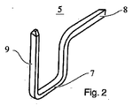
図2は、先行技術によるこのような接触部5の透視図を概略的に示している。
FIG. 2 schematically shows a perspective view of such a
ハウジングの半分2、3の少なくとも一つにおいて、接触部5の信頼性のある機械的で防水性の配置を可能にするように、接触部5は、好ましくはハウジングの材料によって、中央の領域7においてオーバーモールドされる。接触部5のそれぞれの内側の端部9も、電子回路4における受け取り部に対応するように形成され、電子回路基板4は接触部5に嵌合され、接続され、例えば溶接され、好ましくは統合的に接着される。
In order to allow a reliable mechanical and waterproof arrangement of the
ハウジングの半分2、3は、好ましくは熱塑性高分子材料の基礎の上に形成され、ひとたび回路基板4が接触部5の位置に設置されると、従来の手段によって、特に溶接の加工による統合的な接着によって相互接続される。このような溶接は、振動溶接過程により特に好ましく達成される。
The housing halves 2, 3 are preferably formed on the basis of a thermoplastic polymer material, and once the
図3は、翼型の延長部10を有するこの発明による接触部5の透視図を概略的に示している。この発明によると、接触部5の内側の端部9は、少なくともある領域において柔軟である、少なくとも1つの、好ましくは2つの翼型の延長部10を有している。この場合、翼型の延長部10は、好ましくは接触部5の反対側に配置される。
FIG. 3 schematically shows a perspective view of a
接触部5は、導電性のある、好ましくは金属材料の基礎の上に形成され、翼型の延長部10はその上の一つの部品に形成されるか又は成型される。
The
図4は、この発明による接触部5を有する下側のハウジングの半分3の透視図を概略的に示している。
FIG. 4 schematically shows a perspective view of the lower housing half 3 with the
図5は、回路基板4と接触する翼型の延長部10を有する複数の接触部5を設置する手順の平面図を概略的に示している。
FIG. 5 schematically shows a plan view of a procedure for installing a plurality of
凹部12(接触凹部12とも称される)は、正面の電子回路基板4の上に、各接触部5の内側の端部9に対応するように、特に、その翼型の延長部10に対応するように設置される。この場合、凹部12は、例えば、丸い端部を有するスリット状に形成される。凹部12は、導電性のある、好ましくは金属の表面を有し、回路基板4は接触部5の翼型の延長部10に接触するように設置することができるようになる。
The recess 12 (also referred to as contact recess 12) corresponds to the
図6は、回路基板4と接触する複数の接触部5を設置する完全な手順の平面図を概略的に示している。
FIG. 6 schematically shows a plan view of a complete procedure for installing a plurality of
電子回路基板を受け入れるか又は取り囲むハウジング13において接触部5と接触する電子回路基板4を設置する方法では、接触部5の内側の端部9が、回路基板4の各凹部12において翼型の延長部10とともに配置されるように、アセンブリMの方向にハウジング13に挿入されるか又は押し込まれる。この場合、柔軟な翼型の延長部10は、変形され、この変形に対する抵抗力が発生し、よって回路基板4における凹部12に耐力を加える。
In the method of installing the
したがって、信頼性のある電気接触部は、接触部5と電子回路基板4の各凹部12との間で、特に耐力の効果によって可能になり、このような電気接触部は、従来の溶接による組み立てに対し、特に振動に対して耐久性がある。
Therefore, a reliable electrical contact portion is possible between the
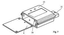
図7は、回路基板4についての正面の受け入れ開口14を有するハウジング13の透視図を概略的に示している。先行技術とは対照的に、回路基板4は、この手順が好ましくはハウジング13の正面の受け入れ開口14を介して行われることができるように、その接触部5と翼型の延長部10とに正面から押し込まれる。したがって、ハウジングは、垂直に分割され、横方向のガイドレールがハウジングにおいて回路基板4のために形成することができ、このレールは組み立て過程を簡易化する。
FIG. 7 schematically shows a perspective view of the
変形例(図示しない)において、この発明による接触部5は、先行技術に従い水平に分割されたハウジングにおいて翼型の延長部10とともに使用することができる。
In a variant (not shown), the
図8は、回路基板について正面に受け入れ開口を有するハウジングと、このハウジングに配置された回路基板4との透視図を概略的に示している。
FIG. 8 schematically shows a perspective view of a housing having a receiving opening in front of the circuit board and the
1 制御ユニット
2 上側のハウジングの半分
3 下側のハウジングの半分
4 電子回路基板
5 接触要素
6 内部の空間
7 中央の領域
8 第1の端部
9 第2の端部
10 翼形状の延長部
11 プラグ接続
12 接触凹部
13 ハウジング
14 受け入れ開口
M 組み立て方向
DESCRIPTION OF
Claims (11)
前記電子回路基板(4)は、前記ハウジング(13)に受け入れられ、
前記電子回路基板(4)は、複数の接触凹部(12)を含み、
前記接触要素(5)は、前記ハウジング(13)の外側の第1の端部(8)及び前記ハウジング(13)の内側の第2の端部(9)を含み、
前記接触要素(5)のそれぞれは、前記第2の端部(9)の位置において、第1の休止位置及び第2の接触位置に位置することができる少なくとも一つの柔軟な延長部(10)を含み、
この方法は、
前記電子回路基板(4)が、前記接触要素(5)の第2の端部(9)が前記接触凹部(12)に対向するように、前記ハウジング(13)に対して位置決めされ、前記柔軟な延長部(10)が、その第1の位置に位置決めされている第1のステップと、
前記電子回路基板(4)が、一方で、前記複数の接触凹部(12)、他方で、前記接触要素(5)の第2の端部(9)の柔軟な延長部(10)によって電気的に接触され、前記柔軟な延長部(10)が、その第2の位置に位置決めされている第2のステップとを
含むことを特徴とする方法。 A method of installing an electronic circuit board (4) that contacts a plurality of contact elements (5) in a housing (13) that receives or surrounds the electronic circuit board (4), comprising:
The electronic circuit board (4) is received in the housing (13);
The electronic circuit board (4) includes a plurality of contact recesses (12),
The contact element (5) includes an outer first end (8) of the housing (13) and an inner second end (9) of the housing (13);
Each of the contact elements (5) is at least one flexible extension (10) that can be located in a first rest position and a second contact position at the position of the second end (9). Including
This method
The electronic circuit board (4) is positioned relative to the housing (13) such that a second end (9) of the contact element (5) faces the contact recess (12), and the flexible A first step in which a flexible extension (10) is positioned in its first position;
The electronic circuit board (4) is electrically connected on the one hand by the plurality of contact recesses (12) and on the other hand by a flexible extension (10) of the second end (9) of the contact element (5). And a second step in which the flexible extension (10) is positioned in its second position.
前記電子回路基板(4)は、複数の接触凹部(12)を含み、
前記接触要素(5)は、前記ハウジング(13)の外側の第1の端部(8)及び前記ハウジング(13)の内側の第2の端部(9)を含み、
前記接触要素(5)のそれぞれは、その第2の端部(9)の位置において、第1の休止位置及び第2の接触位置に位置決めすることができる少なくとも一つの柔軟な延長部(10)を含み、前記電子回路基板(4)は、一方で、前記複数の接触凹部(12)によって、他方で、前記接触要素(5)の前記第2の端部(9)の前記柔軟な延長部(10)によって、電気的に接続され、前記柔軟な延長部(10)は、その第2の位置に位置決めされていることを特徴とするハウジング(13)。 A housing (13) having a contact element (5) in contact with an electronic circuit board (4), said housing (13) receiving or enclosing the electronic circuit board (4);
The electronic circuit board (4) includes a plurality of contact recesses (12),
The contact element (5) includes an outer first end (8) of the housing (13) and an inner second end (9) of the housing (13);
Each of the contact elements (5) has at least one flexible extension (10) that can be positioned in a first rest position and a second contact position at the position of its second end (9). The electronic circuit board (4) on the one hand by the plurality of contact recesses (12) and on the other hand the flexible extension of the second end (9) of the contact element (5) The housing (13) characterized in that it is electrically connected by (10) and the flexible extension (10) is positioned in its second position.
Applications Claiming Priority (5)
| Application Number | Priority Date | Filing Date | Title |
|---|---|---|---|
| DE102011119576 | 2011-11-26 | ||
| DE102011119576.2 | 2011-11-26 | ||
| FR12/01226 | 2012-04-26 | ||
| FR1201226A FR2983386B1 (en) | 2011-11-26 | 2012-04-26 | METHOD FOR CONTACTING AN ELECTRONIC PRINTED CARD WITH A PLURALITY OF CONTACTING ELEMENTS IN A RECEIVING HOUSING OR COVERING THE ELECTRONIC PRINTED BOARD AND HOUSING |
| PCT/EP2012/071635 WO2013075919A1 (en) | 2011-11-26 | 2012-10-31 | Method for placing an electronic printed card in contact with a plurality of contact elements in a housing receiving or surrounding the electronic printed card and housing |
Related Child Applications (1)
| Application Number | Title | Priority Date | Filing Date |
|---|---|---|---|
| JP2017126997A Division JP2017201631A (en) | 2011-11-26 | 2017-06-29 | Method for placing electronic circuit board in contact with plurality of contact elements in housing receiving or surrounding the electronic circuit board, and housing |
Publications (1)
| Publication Number | Publication Date |
|---|---|
| JP2014533878A true JP2014533878A (en) | 2014-12-15 |
Family
ID=48366058
Family Applications (2)
| Application Number | Title | Priority Date | Filing Date |
|---|---|---|---|
| JP2014542752A Pending JP2014533878A (en) | 2011-11-26 | 2012-10-31 | Method and housing for installing an electronic circuit board that contacts a plurality of contact elements in a housing that receives or surrounds the electronic circuit board |
| JP2017126997A Pending JP2017201631A (en) | 2011-11-26 | 2017-06-29 | Method for placing electronic circuit board in contact with plurality of contact elements in housing receiving or surrounding the electronic circuit board, and housing |
Family Applications After (1)
| Application Number | Title | Priority Date | Filing Date |
|---|---|---|---|
| JP2017126997A Pending JP2017201631A (en) | 2011-11-26 | 2017-06-29 | Method for placing electronic circuit board in contact with plurality of contact elements in housing receiving or surrounding the electronic circuit board, and housing |
Country Status (6)
| Country | Link |
|---|---|
| US (1) | US9374917B2 (en) |
| EP (1) | EP2783423B1 (en) |
| JP (2) | JP2014533878A (en) |
| CN (1) | CN104094473B (en) |
| FR (1) | FR2983386B1 (en) |
| WO (1) | WO2013075919A1 (en) |
Families Citing this family (4)
| Publication number | Priority date | Publication date | Assignee | Title |
|---|---|---|---|---|
| DE102014213957B4 (en) * | 2014-07-17 | 2017-10-19 | Robert Bosch Gmbh | Electronic module with inserted electrical contact |
| DE102014213954B4 (en) * | 2014-07-17 | 2017-10-19 | Robert Bosch Gmbh | Electronic module with inserted electrical contact |
| CN107920431B (en) * | 2016-10-11 | 2023-10-13 | 芋头科技(杭州)有限公司 | Circuit board assembly structure |
| DE102019129448B3 (en) | 2019-10-31 | 2020-12-31 | Harting Electric Gmbh & Co. Kg | Housings for electronic components |
Citations (3)
| Publication number | Priority date | Publication date | Assignee | Title |
|---|---|---|---|---|
| JPH04277474A (en) * | 1991-03-05 | 1992-10-02 | Murata Mfg Co Ltd | Connecting structure of connector terminal |
| JPH0673876U (en) * | 1993-03-31 | 1994-10-18 | 第一電子工業株式会社 | Rectangular PCB connector |
| JP2010501993A (en) * | 2006-08-30 | 2010-01-21 | ローベルト ボツシユ ゲゼルシヤフト ミツト ベシユレンクテル ハフツング | Push pin |
Family Cites Families (10)
| Publication number | Priority date | Publication date | Assignee | Title |
|---|---|---|---|---|
| JPH04328282A (en) * | 1991-04-26 | 1992-11-17 | Nec Corp | Hybrid integrated circuit device |
| JPH0538772U (en) * | 1991-10-25 | 1993-05-25 | 東光株式会社 | Electronic component terminal mounting structure |
| DE4324917A1 (en) * | 1992-07-27 | 1994-02-03 | Grote & Hartmann | Electrical contact element for circuit board edge connection - is formed in one piece with claws around rim of inserted conductor, and flanges which contact top and underside of notch in edge of board. |
| US6135781A (en) * | 1996-07-17 | 2000-10-24 | Minnesota Mining And Manufacturing Company | Electrical interconnection system and device |
| US5910025A (en) * | 1997-10-31 | 1999-06-08 | Ericsson, Inc. | Edge interface electrical connectors |
| JP3798177B2 (en) * | 1999-04-06 | 2006-07-19 | 矢崎総業株式会社 | Board connector |
| US6293833B1 (en) * | 2001-01-05 | 2001-09-25 | Yazaki North America | Low insertion force, high contact force terminal spring |
| JP2006216313A (en) * | 2005-02-02 | 2006-08-17 | Sumitomo Wiring Syst Ltd | Terminal fitting |
| DE102006025977B4 (en) * | 2006-06-02 | 2008-10-23 | Siemens Ag Österreich | Control unit with a front side contacted circuit carrier |
| CN201238087Y (en) * | 2008-07-04 | 2009-05-13 | 上海莫仕连接器有限公司 | Conducting terminal for electric connector |
-
2012
- 2012-04-26 FR FR1201226A patent/FR2983386B1/en not_active Expired - Fee Related
- 2012-10-31 CN CN201280067477.0A patent/CN104094473B/en not_active Expired - Fee Related
- 2012-10-31 WO PCT/EP2012/071635 patent/WO2013075919A1/en active Application Filing
- 2012-10-31 US US14/360,569 patent/US9374917B2/en not_active Expired - Fee Related
- 2012-10-31 JP JP2014542752A patent/JP2014533878A/en active Pending
- 2012-10-31 EP EP12783575.9A patent/EP2783423B1/en not_active Not-in-force
-
2017
- 2017-06-29 JP JP2017126997A patent/JP2017201631A/en active Pending
Patent Citations (3)
| Publication number | Priority date | Publication date | Assignee | Title |
|---|---|---|---|---|
| JPH04277474A (en) * | 1991-03-05 | 1992-10-02 | Murata Mfg Co Ltd | Connecting structure of connector terminal |
| JPH0673876U (en) * | 1993-03-31 | 1994-10-18 | 第一電子工業株式会社 | Rectangular PCB connector |
| JP2010501993A (en) * | 2006-08-30 | 2010-01-21 | ローベルト ボツシユ ゲゼルシヤフト ミツト ベシユレンクテル ハフツング | Push pin |
Also Published As
| Publication number | Publication date |
|---|---|
| CN104094473B (en) | 2017-02-22 |
| WO2013075919A1 (en) | 2013-05-30 |
| US9374917B2 (en) | 2016-06-21 |
| EP2783423B1 (en) | 2018-12-05 |
| CN104094473A (en) | 2014-10-08 |
| FR2983386B1 (en) | 2015-06-12 |
| FR2983386A1 (en) | 2013-05-31 |
| JP2017201631A (en) | 2017-11-09 |
| EP2783423A1 (en) | 2014-10-01 |
| US20140321082A1 (en) | 2014-10-30 |
Similar Documents
| Publication | Publication Date | Title |
|---|---|---|
| JP2017201631A (en) | Method for placing electronic circuit board in contact with plurality of contact elements in housing receiving or surrounding the electronic circuit board, and housing | |
| US9634407B2 (en) | Terminal module | |
| EP2560242A1 (en) | Electronic component | |
| JP6269451B2 (en) | Electrical connection structure | |
| JP4851243B2 (en) | Joint connector with built-in capacitor | |
| EP3598583B1 (en) | Electronic device having fixed electric conductive plate and flexible electric conductive plate | |
| CN104518300B (en) | Electronic circuit device | |
| CN108574151B (en) | Mounting aid for mounting electrical components on a printed circuit board and mounting method | |
| JP4820241B2 (en) | Wiring board storage structure | |
| KR101702548B1 (en) | Switch device | |
| US20200045839A1 (en) | Electronic Module and Method for Producing an Electronic Module | |
| JP5669076B2 (en) | Substrate fixing structure and physical quantity sensor | |
| JP2013084476A5 (en) | ||
| JP7094087B2 (en) | Battery device | |
| KR102292756B1 (en) | Housings for electrical components and methods for connecting a housing body to a housing cover | |
| JP5931095B2 (en) | Direct plug-in element with two spring areas | |
| JP6613129B2 (en) | Metal terminal | |
| JP3186949U (en) | Electrical connector | |
| JP2011129011A (en) | Personal digital assistant | |
| JP6954774B2 (en) | Controller unit | |
| KR102542322B1 (en) | Electronic parts | |
| JP2003051652A (en) | Wiring unit | |
| JP2015204311A (en) | Electronic apparatus | |
| JP4911025B2 (en) | Electronics | |
| JP6023397B2 (en) | Conductive connection method between connection terminal and connection member |
Legal Events
| Date | Code | Title | Description |
|---|---|---|---|
| A621 | Written request for application examination |
Free format text: JAPANESE INTERMEDIATE CODE: A621 Effective date: 20151019 |
|
| A977 | Report on retrieval |
Free format text: JAPANESE INTERMEDIATE CODE: A971007 Effective date: 20160812 |
|
| A131 | Notification of reasons for refusal |
Free format text: JAPANESE INTERMEDIATE CODE: A131 Effective date: 20160816 |
|
| A601 | Written request for extension of time |
Free format text: JAPANESE INTERMEDIATE CODE: A601 Effective date: 20161115 |
|
| A521 | Written amendment |
Free format text: JAPANESE INTERMEDIATE CODE: A523 Effective date: 20170210 |
|
| A02 | Decision of refusal |
Free format text: JAPANESE INTERMEDIATE CODE: A02 Effective date: 20170228 |