JP2014503988A - Semiconductor capacitor - Google Patents
Semiconductor capacitor Download PDFInfo
- Publication number
- JP2014503988A JP2014503988A JP2013537667A JP2013537667A JP2014503988A JP 2014503988 A JP2014503988 A JP 2014503988A JP 2013537667 A JP2013537667 A JP 2013537667A JP 2013537667 A JP2013537667 A JP 2013537667A JP 2014503988 A JP2014503988 A JP 2014503988A
- Authority
- JP
- Japan
- Prior art keywords
- metal
- conductive layer
- opening
- conductive
- contact
- Prior art date
- Legal status (The legal status is an assumption and is not a legal conclusion. Google has not performed a legal analysis and makes no representation as to the accuracy of the status listed.)
- Pending
Links
Images


Classifications
-
- H—ELECTRICITY
- H01—ELECTRIC ELEMENTS
- H01L—SEMICONDUCTOR DEVICES NOT COVERED BY CLASS H10
- H01L28/00—Passive two-terminal components without a potential-jump or surface barrier for integrated circuits; Details thereof; Multistep manufacturing processes therefor
- H01L28/40—Capacitors
- H01L28/60—Electrodes
- H01L28/82—Electrodes with an enlarged surface, e.g. formed by texturisation
- H01L28/90—Electrodes with an enlarged surface, e.g. formed by texturisation having vertical extensions
- H01L28/91—Electrodes with an enlarged surface, e.g. formed by texturisation having vertical extensions made by depositing layers, e.g. by depositing alternating conductive and insulating layers
Abstract
大きな面積プレートおよび小さなフットプリントを有する半導体キャパシタ(100、150)が半導体ウエハ(310)上に形成される。この半導体キャパシタは、ウエハ(310)内に開口(320)を形成し、開口(320)内に第1の金属層を形成するようにウエハ(310)から離間して位置する第1のシャドーマスク(214A)を介して第1の金属原子(326)を堆積して、第1の金属層(330)上に誘電体層(334)を形成し、誘電体層(334)上に第2の金属層(342)を形成するようにウエハ(310)から離間して位置する第2のシャドーマスク(214B)を介して第2の金属原子(340)を堆積することにより形成される。
Semiconductor capacitors (100, 150) having a large area plate and a small footprint are formed on a semiconductor wafer (310). The semiconductor capacitor has a first shadow mask positioned away from the wafer (310) so as to form an opening (320) in the wafer (310) and form a first metal layer in the opening (320). Depositing a first metal atom (326) via (214A) to form a dielectric layer (334) on the first metal layer (330) and a second layer on the dielectric layer (334); Formed by depositing second metal atoms (340) through a second shadow mask (214B) that is positioned away from the wafer (310) to form a metal layer (342).
Description
本発明は半導体キャパシタに関し、特に、シャドーマスクと2つのみのリソグラフィ工程で形成される、大きな面積のプレートおよび小さなフットプリントとを備えた半導体キャパシタに関する。 The present invention relates to a semiconductor capacitor, and more particularly to a semiconductor capacitor having a large area plate and a small footprint formed by a shadow mask and only two lithography processes.
半導体キャパシタは、誘電体層によって垂直方向に隔てられた2つの金属プレートを典型的に含む構造として周知である。半導体キャパシタは、通常、金属相互接続構造の一部として形成され、その構造により、追加のリソグラフィ工程を必要とすることなくキャパシタが形成され得る。 Semiconductor capacitors are well known as structures that typically include two metal plates that are vertically separated by a dielectric layer. Semiconductor capacitors are typically formed as part of a metal interconnect structure that allows the capacitor to be formed without the need for additional lithographic steps.
例えば、下方のキャパシタプレートは、第1の金属層がエッチングされて金属トレースの第1の層を形成するのと同時に形成され得、上方のキャパシタプレートは、第2の金属層がエッチングされて金属トレースの第2の層を形成するのと同時に形成され得る。この場合、金属トレースの第1の層を金属トレースの第2の層から電気的に絶縁する層間絶縁膜は、キャパシタ誘電体として機能する。 For example, the lower capacitor plate can be formed at the same time as the first metal layer is etched to form the first layer of metal traces, and the upper capacitor plate can be formed by etching the second metal layer and metal. Can be formed simultaneously with forming the second layer of traces. In this case, the interlayer dielectric that electrically insulates the first layer of metal traces from the second layer of metal traces functions as a capacitor dielectric.
金属相互接続構造の一部として形成されるキャパシタは追加のリソグラフィ工程を必要とせず、それゆえ費用はかからないが、キャパシタの静電容量は、金属相続接続構造の利用可能面積および要件によって制限される。言い換えれば、キャパシタに占有され得る面積と、金属トレースの第1および第2の層間の垂直方向の間隔と、層間絶縁膜として使用される材料とが、キャパシタの要件によってではなく、金属相互接続構造の要件によって規定される。 Capacitors formed as part of the metal interconnect structure do not require additional lithographic steps and are therefore not expensive, but the capacitance of the capacitor is limited by the available area and requirements of the metal interconnect structure . In other words, the area that can be occupied by the capacitor, the vertical spacing between the first and second layers of the metal trace, and the material used as the interlayer dielectric are not dependent on the requirements of the capacitor, but the metal interconnect structure. Stipulated by the requirements of
金属相互接続構造の要件によって規定されないとき、キャパシタによって提供される静電容量は、高誘電率(High K)材料のような異なる誘電材料を利用することによって増加し得る。また、静電容量は、プレートの面積を増加させることによって増加し得る。大きな面積のプレートと小さなフットプリントとを備えるキャパシタを形成するための1つの一般的なアプローチは、基板内に異方性ドライエッチされた開口にコンフォーマルに(conformally)裏打ちするようにプレートを形成することである。 When not defined by the requirements of the metal interconnect structure, the capacitance provided by the capacitor can be increased by utilizing different dielectric materials, such as high dielectric constant (High K) materials. The capacitance can also be increased by increasing the area of the plate. One common approach to form capacitors with large area plates and small footprints is to form the plates conformally backed by anisotropic dry-etched openings in the substrate. It is to be.
大きな面積のプレートと小さなフットプリントとを備えるキャパシタを形成するための別の一般的なアプローチは、小さな面積の交互配置されたプレートを多数使用することであり、奇数プレートの各々が共に接続されて第1のキャパシタプレートを形成し、偶数プレートの各々が共に接続されて第2のキャパシタプレートを形成する。それゆえ、たとえ各プレートの面積が小さくても、第1および第2のキャパシタプレートの有効面積はより大きい。さらなるアプローチは、基板内に異方性ドライエッチされた開口に交互配置されたプレートを多数形成することである。 Another common approach for forming capacitors with large area plates and small footprints is to use a large number of small area interleaved plates, each of the odd plates being connected together. A first capacitor plate is formed and each of the even plates are connected together to form a second capacitor plate. Therefore, even if the area of each plate is small, the effective area of the first and second capacitor plates is larger. A further approach is to form a number of plates interleaved with openings that have been anisotropically dry etched in the substrate.
しかしながら、キャパシタによって提供される静電容量を増加させるためのこれらのアプローチは、典型的に多くのリソグラフィ工程を必要とする。リソグラフィは、半導体製造プロセスにおいて最も費用のかかる工程の1つである。さらに、基板内に異方性ドライエッチされた開口内にコンフォーマルに裏打ちするようにキャパシタプレートが形成されるとき、キャパシタを形成するよう堆積された材料は不均一な厚さを有する傾向にあり、かつ、開口の底面と垂直な側壁とが交差する開口底部の角で非常に薄くなる傾向がある。その結果、これらのキャパシタはより高い不良率を有する傾向がある。 However, these approaches to increase the capacitance provided by the capacitor typically require many lithographic steps. Lithography is one of the most expensive steps in the semiconductor manufacturing process. Further, when a capacitor plate is formed to conformally back in an opening that has been anisotropically dry etched in the substrate, the material deposited to form the capacitor tends to have a non-uniform thickness. In addition, the bottom of the opening and the vertical side wall tend to be very thin at the corner of the bottom of the opening. As a result, these capacitors tend to have a higher failure rate.
それゆえ、限られた数のリソグラフィ工程で形成される、大きな面積のプレートと小さなフットプリントとを有するキャパシタが必要とされる。 Therefore, there is a need for a capacitor with a large area plate and a small footprint that is formed in a limited number of lithography steps.
本発明のキャパシタは、大きな面積のプレートと小さなフットプリントとを提供する。本発明のキャパシタは、半導体ウエハ内の開口と、開口内に位置しかつ半導体ウエハに接する第1の非導電層とを含む。第1の非導電層は実質的に均一の厚さを有する。キャパシタはまた、開口内に位置しかつ第1の非導電層に接する第1の導電構造を有する。第1の導電構造は実質的に均一の厚さを有する。キャパシタはさらに、開口内に位置しかつ第1の非導電層および第1の導電構造に接する第2の非導電層を有する。第2の非導電層は実質的に均一の厚さを有する。キャパシタはさらに、開口内に位置しかつ第2の非導電層に接する第2の導電構造を有する。第2の導電性構造は実質的に均一の厚さを有する。 The capacitor of the present invention provides a large area plate and a small footprint. The capacitor of the present invention includes an opening in the semiconductor wafer and a first nonconductive layer located in the opening and in contact with the semiconductor wafer. The first non-conductive layer has a substantially uniform thickness. The capacitor also has a first conductive structure located in the opening and in contact with the first non-conductive layer. The first conductive structure has a substantially uniform thickness. The capacitor further has a second non-conductive layer located in the opening and in contact with the first non-conductive layer and the first conductive structure. The second non-conductive layer has a substantially uniform thickness. The capacitor further has a second conductive structure located in the opening and in contact with the second non-conductive layer. The second conductive structure has a substantially uniform thickness.
本発明のキャパシタの形成方法の一つは、半導体ウエハに第1の開口を形成すること、および半導体ウエハに接するよう第1の開口内に第1の非導電層を形成することを含む。第1の非導電層は、実質的に均一の厚さを有し、第2の開口を形成する。この方法はまた、複数の第1の原子を第1の非導電層上に堆積させて、第1の非導電性層に接する第1の金属構造を第2の開口内に形成することを含む。第1の原子は第1のシャドーマスクを通過する。第1のシャドーマスクは第1の非導電層の上面から離間される。第1の金属構造は、実質的に均一の厚さを有し、第3の開口を形成する。この方法はさらに、第1の非導電層および第1の金属構造に接する第2の非導電層を第3の開口内に形成することを含む。第2の非導電層は、実質的に均一の厚さを有し、第4の開口を形成する。この方法はさらに、第2の非導電層に複数の第2の原子を堆積させて、第2の非導電層に接する第2の金属構造を第4の開口内に形成することを含む。第2の原子は第2のシャドーマスクを通過する。第2のシャドーマスクは、第2の非導電層の上面から離間される。第2の金属構造は実質的に均一の厚さを有する。 One method of forming a capacitor of the present invention includes forming a first opening in a semiconductor wafer and forming a first non-conductive layer in the first opening so as to contact the semiconductor wafer. The first non-conductive layer has a substantially uniform thickness and forms a second opening. The method also includes depositing a plurality of first atoms on the first non-conductive layer to form a first metal structure in contact with the first non-conductive layer in the second opening. . The first atom passes through the first shadow mask. The first shadow mask is spaced from the top surface of the first non-conductive layer. The first metal structure has a substantially uniform thickness and forms a third opening. The method further includes forming a second non-conductive layer in contact with the first non-conductive layer and the first metal structure in the third opening. The second non-conductive layer has a substantially uniform thickness and forms a fourth opening. The method further includes depositing a plurality of second atoms in the second non-conductive layer to form a second metal structure in contact with the second non-conductive layer in the fourth opening. The second atom passes through the second shadow mask. The second shadow mask is spaced from the top surface of the second non-conductive layer. The second metal structure has a substantially uniform thickness.
図1Aおよび図1Bは、本発明によるキャパシタの一例を説明する図を示す。下記でより詳細に述べるように、本発明は、シャドーマスクと2つのみのリソグラフィステップで形成される、大きな面積のプレートおよび小さなフットプリントとを備えるキャパシタである。 1A and 1B are diagrams illustrating an example of a capacitor according to the present invention. As will be described in more detail below, the present invention is a capacitor comprising a shadow mask and a large area plate and a small footprint formed with only two lithography steps.
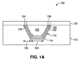
図1Aは、本発明の第1の実施例によるキャパシタ100の一例を説明する断面図を示す。図1Aの例に示すように、キャパシタ100は、半導体基板110と、半導体基板110内の開口112とを含む。
FIG. 1A is a cross-sectional view illustrating an example of a
図1Aの例にさらに示されるように、キャパシタ100は、開口112内に位置しかつ半導体基板110に接する非導電層114を含む。非導電層114は、実質的に均一の厚さを有する。キャパシタ100はまた、完全に開口112に位置しかつ非導電層114に接する導電構造116を含む。非導電層114と同様に、導電構造116もまた実質的に均一の厚さを有する。
As further shown in the example of FIG. 1A, the
さらに、キャパシタ100は、完全に開口112内に位置しかつ非導電層114と導電構造116とに接する非導電層120を含む。さらに、キャパシタ100は、完全に開口112内に位置しかつ非導電層120に接する導電構造122を含む。上述のように、非導電層120と導電構造122とはそれぞれ実質的に均一の厚さを有する。
図1Aの例にさらに示されるように、導電構造116および122は、導電構造116の第1の部分124が、導電構造122の垂直方向の下方に位置し、導電構造116の第2の部分126が、導電構造122のどの部分の垂直方向の下方にも位置しないように、開口122内に配置される。
As further shown in the example of FIG. 1A,
さらに、キャパシタ100は、完全に開口112内に位置しかつ非導電層120および導電構造122に接する非導電領域130を含む。さらにキャパシタ100は、半導体基板110、非導電層114、導電構造116、非導電層120、導電構造122、および非導電領域130に接する非導電層132を含む。
キャパシタ100はまた、金属コンタクト134と金属コンタクト136とを含む。金属コンタクト134は、金属コンタクト134の底面が導電構造116に電気的に接続するように非導電層132を介して延在する。同様に、金属コンタクト136は、金属コンタクト136の底面が導電構造122に電気的に接続するように非導電層130を介して延在する。
金属コンタクト134および金属コンタクト136の双方は、半導体基板110から電気的に絶縁される。さらに、金属コンタクト134は、導電構造122から離間されかつ電気的に絶縁され、金属コンタクト136は、導電構造116から離間されかつ電気的に絶縁される。
Both
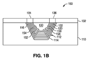
図1Bは、本発明の第2の実施例によるキャパシタ150の一例を説明する断面図を示す。キャパシタ150はキャパシタ100と類似しており、その結果として、双方のキャパシタに共通の要素を示すために同じ参照番号を使用する。
FIG. 1B shows a cross-sectional view illustrating an example of a
図1Bの例に示されるように、キャパシタ150がキャパシタ100と異なるのは、キャパシタ150がさらに、完全に開口112内に位置しかつ非導電層120および導電構造122に接する非導電層152を含む点である。キャパシタ150はまた、完全に開口112内に位置しかつ非導電層152に接する導電構造154を含む。
As shown in the example of FIG. 1B,
さらにキャパシタ150は、完全に開口112内に位置しかつ非導電層152および導電構造154に接する非導電層156を含む。さらにキャパシタ150は、完全に開口112内に位置しかつ非導電領域130および非導電層156に接する導電構造158を含む。上述のように、非導電層152、導電構造154、非導電層156、および導電構造158はそれぞれ実質的に均一の厚さを有する。
導電構造154および158は、実質的に全ての導電構造154が導電構造116の垂直方向の上方に位置し、かつ実質的に全ての導電構造158が、導電構造122の垂直方向の上方に位置するように、開口112内に配置される。さらに非導電層132はまた、非導電層152、導電構造154、非導電層156、および導電構造158に接する。
さらに、金属コンタクト134の底面は、導電構造154に電気的に接続され、他方、金属コンタクト134は、導電構造158から離間されかつ電気的に絶縁される。同様に、金属コンタクト136の底面は、導電構造158に電気的に接続され、他方、金属コンタクト136は、導電構造154から離間されかつ電気的に絶縁される。
Further, the bottom surface of the
その結果、キャパシタ150は、導電構造116および154を含む第1のキャパシタプレートと、導電構造122および158とを含む第2のキャパシタプレートとを含む。それゆえ、キャパシタ100で使用される2つの構造116および122と比較すると、キャパシタ150は、4つもしくはそれ以上の交互配置された構造が交互にキャパシタプレートの有効面積を増加させ、それにより静電容量を増加させるように使用され得ることを例示している。それゆえ、開口112内にキャパシタ100および150を形成する結果として、キャパシタ100および150の各々は、大きな面積のプレートと小さなフットプリントとを有する。
As a result,
本発明の方法は、マルチチャンバ半導体処理システムを使用する。マルチチャンバ半導体処理システムは、ウエハを受け取り、システム内の空気圧を大気中の圧力より低いレベルまで減少させ、そして、真空を破壊することなく特定のシーケンスにおいてチャンバからチャンバへウエハを移動させるシステムである。各チャンバでは、ウエハは特定の処理ステップを受ける。 The method of the present invention uses a multi-chamber semiconductor processing system. A multi-chamber semiconductor processing system is a system that receives a wafer, reduces the air pressure in the system to a level below atmospheric pressure, and moves the wafer from chamber to chamber in a specific sequence without breaking the vacuum. . In each chamber, the wafer undergoes specific processing steps.
例えば、マルチチャンバ半導体処理システムは、クラスタツールあるいはシーケンサで実装され得る。クラスタツールは、特定のシーケンスがいずれかのチャンバから任意の他のチャンバまでであることができるように、ランダムアクセスを提供する。他方、シーケンサは、固定されたチャンバのシーケンス(順序)を提供する。 For example, a multi-chamber semiconductor processing system can be implemented with a cluster tool or a sequencer. The cluster tool provides random access so that a particular sequence can be from any chamber to any other chamber. On the other hand, the sequencer provides a fixed chamber sequence.
本発明の第1の実施例では、マルチチャンバ半導体処理システムは、3つのチャンバを含む:誘電体を堆積するための第1のチャンバと、金属を堆積するための第2のチャンバと、金属を堆積するための第3のチャンバである。第1のチャンバは、化学蒸着(CVD)チャンバのような任意の従来の誘電体蒸着チャンバで実装され得る。第2および第3のチャンバは、例えばプラズマ蒸着(PVD)チャンバで実装され得る。 In a first embodiment of the present invention, a multi-chamber semiconductor processing system includes three chambers: a first chamber for depositing a dielectric, a second chamber for depositing metal, and a metal. A third chamber for deposition. The first chamber may be implemented with any conventional dielectric deposition chamber, such as a chemical vapor deposition (CVD) chamber. The second and third chambers may be implemented with, for example, plasma deposition (PVD) chambers.
本発明によれば、マルチチャンバ半導体処理システムの第2および第3チャンバは、ウエハの処理されるべき表面から離間されかつその上に位置するシャドーマスクを含むようにそれぞれ変更される。シャドーマスクは、アルミニウムプレートなどの金属プレートであり、このマスクは、当該金属プレートを完全に貫通するパターンを含むように処理される。 In accordance with the present invention, the second and third chambers of the multi-chamber semiconductor processing system are each modified to include a shadow mask that is spaced from and located above the surface of the wafer to be processed. The shadow mask is a metal plate, such as an aluminum plate, that is processed to include a pattern that completely penetrates the metal plate.
図2Aないし図2Cは、本発明による半導体処理システムの一例を説明する図を示す。図2Aは、本発明による金属蒸着チャンバ200の一例を示す断面図を示す。図2Aに示されるように、動作中に封止される金属蒸着チャンバ200は、チャックなどのウエハ支持210と、ウエハ支持210上に位置しかつウエハ支持210から離間されたターゲット212と、ウエハ支持210とターゲット212との間に位置するシャドーマスク214とを含む。
2A to 2C are diagrams illustrating an example of a semiconductor processing system according to the present invention. FIG. 2A shows a cross-sectional view illustrating an example of a
さらに金属蒸着チャンバ200は、ウエハ支持210、ターゲット212、およびシャドーマスク214を支持するため、ウエハ支持210、ターゲット212、およびシャドーマスク214に接続されたフレーム構造216を含む。シャドーマスク214は、ウエハ支持210とシャドーマスク214間の距離が固定されるように、フレーム構造216にしっかりと取り付けられ得る。
任意選択的に、ウエハ支持210とシャドーマスク214間の距離が変化されてもよい。例えば、フレーム構造216は、シャドーマスク214を垂直方向に移動させる垂直方向のアクチュエータ218を含み得る。代替的に、チャンバ200に挿入されたウエハに係合するように垂直方向に移動可能であり得るウエハ支持210は、ウエハ支持210とシャドーマスク214間の距離を変化させ得る、より大きな垂直方向の伸長を含むよう変更されても良い。
Optionally, the distance between
さらに、追加の柔軟性のために、金属蒸着チャンバ200は、ロボットアームなどのシャドーマスク移動構造を含むことができ、当該移動構造は、シャドーマスク214を所定位置に移動させ、そしてシャドーマスク214を取り外させるように、フレーム構造216に接続される。シャドーマスク移動構造は、チャンバ200を開けることなく、シャドーマスク214用いてあるいは用いないで、金属蒸着チャンバ200を使用できるようにする。
Further, for additional flexibility, the
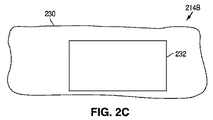
図2Bおよび図2Cは、本発明によるシャドーマスク214の例を説明する平面図を示す。図2Bは、本発明によるシャドーマスク214の第1の例を説明するシャドーマスク214Aを示し、図2Cは、本発明によるシャドーマスク214の第2の例を説明するシャドーマスク214Bを示す。
2B and 2C show plan views illustrating an example of a
図2Bに示されるように、シャドーマスク214Aは、アルミニウムプレートなどの金属プレート220と、金属プレート220を貫通する開口222とを含む。同様に、図2Cに示すように、シャドーマスク214Bは、アルミニウムプレートなどの金属プレート230と、金属プレート230を貫通する開口232とを含む。
As shown in FIG. 2B, the
本発明によれば、マルチチャンバ半導体処理システムの第2のチャンバは、シャドーマスク214がシャドーマスク214Aで実装される金属蒸着チャンバで200で実装され、マルチチャンバ半導体処理システムの第3のチャンバは、シャドーマスク214がシャドーマスク214Bで実装される金属蒸着チャンバ200で実装される。
In accordance with the present invention, the second chamber of the multi-chamber semiconductor processing system is implemented with a
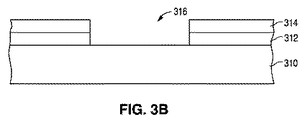
図3Aおよび図3Bは、本発明によるキャパシタの形成方法の第1のステップの一例を説明する図を示す。図3Aは平面図を示し、図3Bは、図3Aの3B−3B線に沿った断面図を示す。図3Aおよび図3Bに示されるように、本発明の方法は、従来の方式で形成された半導体ウエハ310を使用する。本例では、<100>シリコンウエハが使用されるが、他のウエハもまた使用され得る。
3A and 3B are diagrams illustrating an example of the first step of the method for forming a capacitor according to the present invention. 3A shows a plan view, and FIG. 3B shows a cross-sectional view taken along
図3Aおよび図3Bでさらに示されるように、本発明の方法は、従来の方法でウエハ310の上面にマスキング層312を堆積することから始まる。マスキング層312は、例えば、シリコンナイトライドで実装され得る。これに続いて、パターン化されたフォトレジスト層314がマスキング層312の上面上に形成される。
As further shown in FIGS. 3A and 3B, the method of the present invention begins by depositing a
パターン化されたフォトレジスト層312は、従来の方法で形成され、当該方法は、フォトレジスト層を堆積すること、光に曝されたフォトレジスト領域を軟化させるためのマスクとして公知のパターン化された黒/透明ガラスを介して光を投射すること、その後に軟化されたフォトレジスト領域を除去することを含む。
The patterned
パターン化されたフォトレジスト層314が形成された後、マスキング層312の露出された領域が従来の方法でエッチングされて、ウエハ310の上面を露出させる開口316を形成する。ウエハ310の上面が露出されると、パターン化されたフォトレジスト層314が従来の方法で除去される。
After the patterned
図4Aないし図4Cは、本発明によるキャパシタの形成方法の第2のステップの一例を説明する図を示す。図4Aは平面図であり、図4Bは、図4Aの4B−4B線に沿った断面図を示す。図4Cは、代替的な実施例を説明する断面図を示す。
4A to 4C are diagrams illustrating an example of the second step of the method for forming a capacitor according to the present invention. 4A is a plan view, and FIG. 4B is a cross-sectional view taken along
図4Aおよび図4Bに示されるように、パターン化されたフォトレジスト層314の除去に続いて、ウエハ310は、水酸化テトラメチルアンモニウム(TMAH)あるいは水酸化カリウム(KOH)などの従来のエッチャントを用いて従来の方法で異方性ウェットエッチングされて、ウエハ310内に開口320を形成する。図4Aおよび図4Bにさらに示されるように、<100>シリコンウエハの異方性ウェットエッチングが、結晶面に沿ってエッチングをして、平坦な底面と、54.7°相当の角度αを有する垂直でない側壁とを有する開口320を形成する。
As shown in FIGS. 4A and 4B, following removal of the patterned
代替的に、フッ硝酸(HNA)など、結晶面に対し敏感でないウェットエッチャントが、開口320を形成するために、任意のタイプのウエハで使用され得る。図4Cに例示されるように、結晶面に鈍感なエッチャントは、すべての方向に等しくエッチングをし、これにより、平坦な底面と曲線的な側壁とを有する開口320を形成する。図4Bあるいは図4Cに示されるように開口320が形成された後、マスキング層312が従来の方法で除去される。
Alternatively, a wet etchant that is not sensitive to crystal planes, such as hydrofluoric acid (HNA), can be used with any type of wafer to form the
図5は、本発明によるキャパシタの形成方法の第3のステップの結果の一例を説明する断面図を示す。図5に示されるように、開口320が形成され、かつマスキング層312が除去された後、本発明の方法は、ウエハ310をマルチチャンバ半導体処理システムの第1のチャンバへ挿入することにより続行する。
FIG. 5 is a cross-sectional view illustrating an example of the result of the third step of the method for forming a capacitor according to the present invention. After the
第1のチャンバへ挿入されると、実質的に均一の厚さを有する誘電体層322が従来の方法でウエハ310の上面上に堆積される。誘電体層322の堆積は、開口324を形成する。誘電体層322の形成の後、ウエハ310が第1のチャンバから取り除かれる。図5に示されるように、誘電体層322は、開口320をコンフォーマルに裏打ちするように形成される。
When inserted into the first chamber, a
図6は、本発明によるキャパシタの形成方法の第4のステップの一例を説明する断面図を示す。図6に示されるように、ウエハ310が第1のチャンバから取り除かれた後、ウエハ310は、ウエハ支持210上に位置するようマルチチャンバ半導体処理システムの第2のチャンバに挿入される。
FIG. 6 is a sectional view for explaining an example of the fourth step of the capacitor forming method according to the present invention. As shown in FIG. 6, after the
第2のチャンバに挿入されると、多数の第1の金属原子326が従来の方法でターゲット212から遊離される。遊離された第1の金属原子326は、接地されたウエハ310に電気的に引きつけられ、かつシャドーマスク214/214Aを通過して、誘電体層322の上面上に第1の金属構造330を形成する。第1の金属原子326の堆積は、開口332を形成する。
When inserted into the second chamber, a number of
図6に示されるように、シャドーマスク214/214Aにより、第1の金属構造330は、誘電体層322の水平の上面から、開口324の一方の側面を下方に沿い、底面を横切り、かつ開口324の反対側の側面の一部にのみ延在する。その結果、第1の金属構造330は、開口324の一方の側の誘電体層322の水平な上面に接するが、開口324の反対側の誘電体層322の水平な上面には接しない。第1の金属構造330の形成後、ウエハ310は第2のチャンバから取り除かれる。
As shown in FIG. 6, the
従来のPDV処理では、遊離された原子326は非常に異方性である。その結果、第1の金属構造330は、完全には異方性でない遊離された原子326のために傾斜される傾向にある周縁を除き、実質的に均一の厚さを有する。また、特徴の明確さをさらに改善するために、シャドーマスク214/214Aは、誘電体層322に接することなく、できるだけ誘電体層322の上面に近接するように配置され、それによって、シャドーマスク214/214Aを通過する異方性でない原子326の影響を制限する。
In conventional PDV processing, the liberated
図7は、本発明によるキャパシタを形成する方法の第5のステップの結果の一例を説明する断面図を示す。ウエハ310が第2のチャンバから取り除かれた後、ウエハ310がマルチチャンバ半導体処理システムの第1のチャンバへ再び挿入される。
FIG. 7 shows a cross-sectional view illustrating an example of the result of the fifth step of the method of forming a capacitor according to the invention. After the
第1のチャンバに挿入されると、実質的に均一の厚さを有する誘電体層334が誘電体層322の上面および第1の金属構造330の上に従来の方法で堆積される。誘電体層334の堆積は開口336を形成する。誘電体層334の形成後、ウエハ310が第1のチャンバから取り除かれる。図7に示されるように、誘電体層334は、誘電体層322と第1の金属構造330の上にコンフォーマルに形成される。
When inserted into the first chamber, a
図8は、本発明によるキャパシタの形成方法の第6のステップの一例を説明する断面図を示す。図8に示されるように、ウエハ310が第1のチャンバから取り除かれた後、ウエハ310は、ウエハ支持210上に位置するようマルチチャンバ半導体処理システムの第3のチャンバに挿入される。
FIG. 8 is a sectional view for explaining an example of the sixth step of the method for forming a capacitor according to the present invention. As shown in FIG. 8, after the
第3のチャンバに挿入されると、多数の第2の金属原子340がターゲット212から従来の方法で遊離される。遊離された第2の金属原子340は、接地されたウエハ310に電気的に引きつけられ、かつシャドーマスク214/214Bを通過して、誘電体層334の上面上に第2の金属構造342を形成する。第2の金属原子340の堆積は、開口344を形成する。
When inserted into the third chamber, a number of
図8に示されるように、シャドーマスク214/214Bのため、第2の金属構造342は、誘電体層334の水平な上面から、開口336の一方の側面を下方に沿い、底面を横切り、開口336の反対側の一部にのみ延在する。その結果、第2の金属構造342は、開口336の一方の側で誘電体層334の水平な上面に接するが、開口336の反対側の誘電体層334の水平な上面には接しない。第2の金属構造342の形成後、ウエハ310は第3のチャンバから取り除かれる。
As shown in FIG. 8, due to the
上述のように、遊離された原子340は非常に異方性である。その結果、第2の金属構造342は、完全には異方性でない遊離された原子340のため傾斜される傾向にある周縁を除き、実質的に均一の厚さを有する。また、特性の明確さをさらに改善するために、シャドーマスク214/214Bは、誘電体層334に接することなく、できるだけ誘電体層334の上面に近接して配置され、これにより、シャドーマスク214/214Bを通過する異方性でない原子340の影響を制限する。
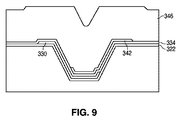
As mentioned above, the liberated
図9は、本発明によるキャパシタの形成方法の第7のステップの結果の一例を説明する断面図を示す。ウエハ310が第3のチャンバから取り除かれた後、ウエハ310は、再びマルチチャンバ半導体処理システムの第1のチャンバに挿入される。第1のチャンバに挿入されると、厚い誘電体層346が誘電体層334の上面と第2の金属構造342上に従来の方法で堆積される。誘電体層346の形成後、ウエハ310は第1のチャンバから取り除かれる。
FIG. 9 is a sectional view for explaining an example of the result of the seventh step of the method for forming a capacitor according to the present invention. After the
金属構造の形成は、第2の金属構造342の形成の後に終了することができ、あるいは代替的に、金属構造の形成は、誘電体層346が形成される前に、追加のn個のラウンドに対し継続することができる。図10は、本発明によるキャパシタの形成方法の追加のn個のラウンドのうちの第2ラウンドの一例を説明する断面図を示す。
The formation of the metal structure can be terminated after the formation of the
図10に示されるように、追加のn個のラウンドの第2ラウンドは、ウエハ310を第1のチャンバへ移動させることによって実行され得、ここで実質的に均一の厚さを有する誘電体層348が、誘電体層334と第2の金属構造342との上に形成される。次に、ウエハ310が第1のチャンバから取り除かれて第2のチャンバに挿入され、ここで第3の金属構造350が誘電体層348上に形成される。これに続いて、ウエハ310が第2のチャンバから第1のチャンバへ移動され、ここで誘電体層352が誘電体層348と第3の金属構造350上に形成される。
As shown in FIG. 10, a second round of additional n rounds can be performed by moving the
この後、ウエハ310が第1のチャンバから第3のチャンバへ移動され、ここで第4の金属構造354が誘電体層352上に形成される。これに続いて、ウエハ310が第3のチャンバから第1のチャンバへ移動され、ここで厚い誘電体層346が誘電体層352と第4の金属構造354との上に形成される。
Thereafter, the
実行される追加のn個のラウンドの数は、開口320の寸法(すなわち、浅い開口320は、多数の金属構造に対応することができない)および上限に制限があるため、取得されるべき静電容量値によって決定される。上限は、不良率と許容可能な故障率によって統計的に決定され得る。例えば、もし、千ラウンド毎に1つのラウンドがキャパシタを故障させる不良を有し、許容可能な故障率がキャパシタ50個につき1つであるならば、各キャパシタは20個のラウンドの上限を含み得る。
The number of additional n rounds performed is limited by the size of the aperture 320 (ie, the
故障の主な原因の1つは、隣接する金属構造を分離する誘電体層中のピンホールの形成である。この結果、誘電体層322、334、346、348、352の各々は、多層の材料から形成され得る。また、これらの多層の材料は、2つあるいはそれ以上の異なるタイプの材料を含み得る。多層の誘電体層は、誘電体層中のピンホールがキャパシタを故障させる可能性を減少させる。(ウエハ310がチャンバからチャンバへと移動するときに真空を維持することもまたピンホール形成の可能性を著しく減らす。)
One major cause of failure is the formation of pinholes in the dielectric layer that separates adjacent metal structures. As a result, each of the
誘電体層322、334、346、348、352は、酸化物、酸窒化物、あるいは窒化物などの従来の誘電材料で実装され得る。さらに、チタン酸バリウムストロンチウム(BST)、酸化チタン(TiOx)、およびチタン酸バリウム(BT)といった焼結を要する他の材料もまた誘電体層を実装するのに使用され得る。このような他の材料は、焼結の要件に起因して使用され得る金属あるいは合金のタイプを決定する。
第2および第3チャンバ内のターゲット212を形成するのに使用される材料は、同一であっても異なっても良く、マルチチャンバシステム内のシャドーマスクを介してコンフォーマルに堆積され得る金属あるいは合金とし得、さらに処理温度やエッチング化学成分など、残る製造要件に耐え得るものである。低いシート抵抗を有するクロムが、第2および第3チャンバ内で金属構造を形成するために堆積され得る材料の一例である。アルミニウムもまた使用され得る材料の一例である。
The material used to form the
図11は、本発明によるキャパシタの形成方法の追加のn個のラウンドと第7のステップとの完了の後に続く次のステップの一例を説明する断面図を示す。図11に示されるように、最後の金属構造342あるいは354が形成された後、ウエハ310がマルチチャンバ半導体処理システムから取り除かれ、そして、化学機械研磨などの従来の方法で平坦化される。
FIG. 11 shows a cross-sectional view illustrating an example of the next step following the completion of the additional n rounds and the seventh step of the method of forming a capacitor according to the present invention. As shown in FIG. 11, after the
図11でさらに示されるように、平坦化は、非導電領域358を形成し、金属構造330、誘電体層334、金属構造342、および誘電体層346(および、存在する場合、誘電体層348、金属構造350、誘電体層352、および誘電体層354)を、ウエハ310の水平な上面上の位置から除去する。
As further shown in FIG. 11, planarization forms a
その結果、金属構造330、誘電体層334、金属構造342、および誘電体層346(および、存在する場合、誘電体層348、金属構造350、誘電体層352、および金属構造354)は、完全に開口320内に位置する。図11に示されるように、誘電体層322がウエハ310の水平な上面から除去された後に、あるいは代替的に、金属構造330が誘電体層322の水平な上面から除去された後に、平坦化が終了し得る。
As a result,
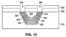
図12は、本発明によるキャパシタ形成方法の平坦化に続く次のステップの一例を説明する断面図を示す。図12に示されるように、平坦化が完了した後、絶縁層360がウエハ310の上面上に従来通り堆積され、パターン化されたフォトレジスト層362の従来通りの形成がそれに続く。絶縁層360は、例えば酸化物で実装され得る。
FIG. 12 is a sectional view for explaining an example of the next step following the planarization of the capacitor forming method according to the present invention. As shown in FIG. 12, after planarization is completed, an insulating
パターン化されたフォトレジスト層362が形成された後、絶縁層360の露出された領域は、従来の方法でエッチングされて、第1の金属構造330(および、存在する場合、第3の金属構造350と、任意の追加の奇数番号の構造と)を露出させる第1の開口364と、第2の金属構造342(および存在する場合、第4の金属構造354と、任意の追加の偶数番号の構造と)を露出させる第2の開口366とを形成する。ウエハ310の上面が露出されると、パターン化されたフォトレジスト層362が従来の方法で除去される。
After the patterned
図13は、本発明によるキャパシタ形成方法のパターン化されたフォトレジスト層362の除去に続く次のステップの一例を説明する断面図を示す。図13に示されるように、パターン化されたフォトレジスト層362が除去された後、コンタクト/ビア材料などの金属性材料が、開口364および366を充填するよう絶縁層360の上面上に堆積され、その後、従来の方法で平坦化されて、第1の開口364内の第1の金属性コンタクト370と第2の開口366内の第2の金属性コンタクト372とを形成する。
FIG. 13 shows a cross-sectional view illustrating an example of the next step following removal of the patterned
第1の金属性コンタクト370は、第1の金属構造330(および存在する場合、第3の金属構造350と、任意の追加の奇数番号の構造と)に接し、第2の金属性コンタクト372は、第2の金属構造342(および存在する場合、第4の金属構造354と、任意の追加の偶数番号の構造と)に接する。これに続いて、この方法は従来のバックエンド処理ステップを続ける。
The first
このように、シャドーマスクを使用して大きな面積のプレートと小さなフットプリントを有する半導体キャパシタを形成する1つの方法が説明された。本発明の利点の1つは、ウエハ内に開口を形成するために異方性ウェットエッチあるいは等方性ウェットエッチの使用によって、キャパシタを形成するために堆積された各材料が(金属層の端部を除いて)均一の厚さで開口に裏打ちされ、これにより、従来のアプローチに関する薄いスポットや非均一の被覆性の問題をなくすことである。 Thus, one method for forming a semiconductor capacitor having a large area plate and a small footprint using a shadow mask has been described. One of the advantages of the present invention is that each material deposited to form a capacitor (the edge of the metal layer) by using an anisotropic or isotropic wet etch to form an opening in the wafer. The opening is lined with a uniform thickness (with the exception of the part), thereby eliminating the thin spots and non-uniform coverage problems associated with conventional approaches.
本発明の別の利点は、本発明が2つのみのリソグラフ工程でキャパシタを形成することである:すなわち、マスキング層312に開口316を形成するために必要なステップと、絶縁層360に開口364と366とを形成するために必要なステップである。さらに、本発明の方法は、多数のプレート、例えば20の奇数プレートと20の偶数プレート、が形成されることを可能にするため、本発明のキャパシタは、例えばマイクロファラッド範囲のような、非常に大きな静電容量値を有することができる。
Another advantage of the present invention is that the present invention forms the capacitor in only two lithographic steps: the steps necessary to form the
図14は、本発明の第2の実施例によるプラズマエッチングチャンバ1400の一例を説明する断面図を示す。図14に示されるように、動作中には封止されるプラズマエッチングチャンバ1400は、チャックなどのウエハ支持1410と、ウエハ支持1410の上方に位置し、かつウエハ支持1410から離間されるRFプラズマ発生器1412とを含む。さらに、プラズマエッチングチャンバ1400はまた、ウエハ支持1410とRFプラズマ発生器1412とを支持するようウエハ支持1410とRFプラズマ発生器1412とに接続されるフレーム構造1414を含む。
FIG. 14 shows a cross-sectional view illustrating an example of a
本発明の第2の実施例によれば、マルチチャンバ半導体処理システムは、プラズマエッチングチャンバ1400で実装されるブランケットプラズマエッチングチャンバを含み得る。本発明の第2の実施例では、各誘電体層の堆積に続いて、かつ次の金属構造が形成される前に、ブランケットプラズマエッチングが実施されて、誘電体層の上面に存在し得る如何なる汚染物質をも除去するために誘電体層の表面層を取り除くことができる。図14は、誘電体層334のブランケットプラズマエッチングを例示している。
In accordance with a second embodiment of the present invention, a multi-chamber semiconductor processing system may include a blanket plasma etch chamber implemented with a
図15Aおよび図15Bは、本発明による定義シャドーマスクの例を説明する平面図を示す。図15Aは、第1の定義シャドーマスク1510を示し、図15Bは、第2の定義シャドーマスク1520を示す。図15Aに示されるように、アルミニウムで実装され得る定義シャドーマスク1510は、シャドーマスク214A内の開口の概ね反転である金属プレート領域1512と、金属プレート領域1512を隣接する構造に接続する多数の支持領域1514とを含む。
15A and 15B show plan views illustrating examples of definition shadow masks according to the present invention. FIG. 15A shows a first
同様に、図15Bに示されるように、アルミニウムで実装され得る定義シャドーマスク1520は、シャドーマスク214B内の開口の概ね反転である金属プレート領域1522と、金属プレート領域1522を隣接する構造に接続する多数の支持体領域1524とを含む。
Similarly, as shown in FIG. 15B, a
図16は、本発明の第3の実施例によるプラズマエッチングチャンバ1600の一例を説明する断面図を示す。図16に示されるように、プラズマエッチングチャンバ1600は、プラズマエッチングチャンバ1400と類似しており、そのため、双方のチャンバに共通する構造を示すのに同じ参照番号が使用される。
FIG. 16 shows a cross-sectional view illustrating an example of a
図16に示されるように、プラズマエッチングチャンバ1600がプラズマエッチングチャンバ1400と異なる点は、プラズマエッチングチャンバ1600がウエハ支持1410とRFプラズマ発生器1412との間に位置するように、フレーム構造1414に接続された定義シャドーマスク1610を含むことである。
As shown in FIG. 16,
本発明の第3の実施例によれば、マルチチャンバ半導体処理システムは、図16に示されるように、定義シャドーマスク1610が定義シャドーマスク1510で実装される、プラズマエッチングチャンバ1600で実装される第1の定義プラズマエッチングチャンバと、定義シャドーマスク1610が定義シャドーマスク1520で実装される、プラズマエッチングチャンバ1600で実装される第2の定義プラズマエッチングチャンバとを含み得る。
In accordance with a third embodiment of the present invention, a multi-chamber semiconductor processing system is implemented in a
本発明の第3の実施例では、例えば第1の金属構造330や第3の金属構造350といった奇数番号の金属構造の各々の堆積に続いて、かつ次の誘電体層が形成される前に、ウエハ310が定義シャドーマスク1610/1510を介してプラズマエッチングされ、金属構造330および350から不所望に離れて延在する金属層を除去する。
In a third embodiment of the present invention, following the deposition of each odd-numbered metal structure, eg,
例えば、薄い金属層が開口324の右側に不所望に延在する可能性があり、その結果、シャドーマスク214Aを通過した異方性のない原子のために、開口324の両側の誘電体層の水平な上面上に金属層が位置する。定義プラズマエッチングは、各金属プレートが開口の片側にのみに位置することを確実にするため、この薄い金属層を除去する。
For example, a thin metal layer may undesirably extend to the right side of the
同様に、例えば、第2の金属構造342や第4の金属構造354といった偶数番号の金属構造の各々の堆積に続いて、かつ次の誘電体層が形成される前に、ウエハ310が定義シャドーマスク1610/1520を介してプラズマエッチングされて、金属構造342および354から不所望に離れて延在するあらゆる金属層を取り除く。
Similarly,
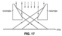
図17は、本発明による定義シャドーマスク1510および1520の支持領域1514および1524の一例を説明する断面図を示す。図17に示されるように、薄い金属層1710が金属構造から不所望に離れて延在するとき、支持領域1514あるいは支持領域1524は(偶数あるいは奇数の金属層のどちらがエッチングされているのかに依り)、プラズマエッチングが支持領域1514あるいは1524の直下に位置する薄い金属層1710を除去するのを遮断する。
FIG. 17 shows a cross-sectional view illustrating an example of
しかしながら、図17にさらに示されるように、支持領域1514および1524の側壁は、各支持体領域1514および1524によって遮断されたプラズマエッチング粒子が反射されて、隣接する支持領域1514および1524の直下に位置する薄い第1の金属層1710を除去するように、角度が付けられている。
However, as further shown in FIG. 17, the sidewalls of
上記説明は本発明の例示であり、ここで説明された発明の様々な代替物が本発明を実施するにあたり採用され得ることが理解されるべきである。それゆえ下記の請求項は本発明の範囲を定義するものであり、これらの請求項の範囲内にある構造および方法とそれらの相当物はこれに含まれることが意図される。
It is to be understood that the above description is illustrative of the invention and that various alternatives to the invention described herein can be employed in practicing the invention. Therefore, the following claims are intended to define the scope of the present invention, and structures and methods within the scope of these claims and their equivalents are intended to be included therein.
Claims (20)
前記開口内に位置し、前記半導体ウエハに接し、かつ実質的に均一の厚さを有する第1の非導電層と、
前記開口内に位置し、前記第1の非導電層に接し、かつ実質的に均一の厚さを有する第1の導電構造と、
前記開口内に位置し、前記第1の非導電層および前記第1の導電構造に接し、かつ実質的に均一の厚さを有する第2の非導電層と、
前記開口内に位置し、前記第2の非導電層に接し、かつ実質的に均一の厚さを有する第2の導電構造と、
を含むキャパシタ。 An opening in the semiconductor wafer;
A first non-conductive layer located within the opening, in contact with the semiconductor wafer and having a substantially uniform thickness;
A first conductive structure located in the opening, in contact with the first non-conductive layer, and having a substantially uniform thickness;
A second non-conductive layer located within the opening, in contact with the first non-conductive layer and the first conductive structure, and having a substantially uniform thickness;
A second conductive structure located within the opening, in contact with the second non-conductive layer, and having a substantially uniform thickness;
Including capacitor.
前記第1の導電構造の第2の部分が、前記第2の導電構造のどの部分の垂直方向の下方にも位置せず、前記第2の部分が前記開口内に位置する、
請求項1に記載のキャパシタ。 A first portion of the first conductive structure is positioned vertically below the second conductive structure, and the first portion is positioned in the opening;
The second portion of the first conductive structure is not located vertically below any portion of the second conductive structure, and the second portion is located in the opening;
The capacitor according to claim 1.
前記第3の非導電層を介して延在して前記第1の導電構造と電気的に接続する第1の金属コンタクトと、
前記第3の非導電層を介して延在して前記第2の導電構造と電気的に接続する第2の金属コンタクトと、
を含む請求項4に記載のキャパシタ。 The capacitor further
A first metal contact extending through the third non-conductive layer and electrically connected to the first conductive structure;
A second metal contact extending through the third non-conductive layer and electrically connected to the second conductive structure;
The capacitor according to claim 4, comprising:
半導体ウエハに第1の開口を形成すること、
前記半導体ウエハに接するように前記第1の開口に第1の非導電層を形成することであって、当該第1の非導電層が実質的に均一の厚さを有しかつ第2の開口を形成すること、
前記第2の開口内に前記第1の非導電層に接する第1の金属構造を形成するように前記第1の非導電層上に複数の第1の原子を堆積することであって、当該第1の原子が第1のシャドーマスクを通過し、当該第1のシャドーマスクが前記第1の非導電層の上面から離間され、前記第1の金属構造が実質的に均一の厚さを有しかつ第3の開口を形成すること、
前記第3の開口内に前記第1の非導電層と前記第1の金属構造とに接するように第2の非導電層を形成することであって、当該第2の非導電層が実質的均一の厚さを有しかつ第4の開口を形成すること、および
前記第4の開口内に前記第2の非導電層に接する第2の金属構造を形成するように前記第2の非導電層上に複数の第2の原子を堆積することであって、当該第2の原子が第2のシャドーマスクを通過し、当該第2のシャドーマスクが前記第2の非導電層の上面から離間され、前記第2の金属構造が実質的に均一の厚さを有すること、
を含む、キャパシタの形成方法。 A method of forming a capacitor, comprising:
Forming a first opening in a semiconductor wafer;
Forming a first non-conductive layer in the first opening so as to contact the semiconductor wafer, the first non-conductive layer having a substantially uniform thickness and a second opening; Forming,
Depositing a plurality of first atoms on the first non-conductive layer to form a first metal structure in contact with the first non-conductive layer in the second opening, The first atoms pass through the first shadow mask, the first shadow mask is spaced from the top surface of the first non-conductive layer, and the first metal structure has a substantially uniform thickness. And forming a third opening,
Forming a second non-conductive layer in contact with the first non-conductive layer and the first metal structure in the third opening, wherein the second non-conductive layer is substantially Forming a fourth opening having a uniform thickness and forming a second metal structure in contact with the second non-conductive layer in the fourth opening. Depositing a plurality of second atoms on the layer, wherein the second atoms pass through a second shadow mask, and the second shadow mask is spaced from the top surface of the second non-conductive layer. The second metal structure has a substantially uniform thickness;
A method for forming a capacitor.
前記第1の金属構造を露出するように前記第3の非導電層に第1の開口を形成し、当該第1の開口の形成と同時に、前記第2の金属構造を露出するように前記第3の非導電層に第2の開口を形成すること、および
前記第1の金属構造と電気的に接するように前記第1の開口に第1の金属コンタクトを形成し、かつ前記第2の金属構造に電気的に接するように前記第2の開口に第2の金属コンタクトを形成すること、
を含む、請求項10に記載の方法。 The method of forming the capacitor further
A first opening is formed in the third non-conductive layer so as to expose the first metal structure, and simultaneously with the formation of the first opening, the first metal structure is exposed so as to expose the second metal structure. Forming a second opening in the three non-conductive layers; and forming a first metal contact in the first opening so as to be in electrical contact with the first metal structure; and the second metal Forming a second metal contact in the second opening so as to be in electrical contact with the structure;
The method of claim 10, comprising:
前記第1の金属構造が形成された後であってかつ前記第2の非導電層が形成される前に、前記第1の金属構造をエッチングするように第1の定義シャドーマスクを原子が通過することであって、当該第1の定義シャドーマスクが前記第1の金属構造の上面から離間されること、および
前記第2の金属構造が形成された後であってかつ前記第3の非導電層が形成される前に、前記第2の金属構造をエッチングするように第2の定義シャドーマスクを原子が通過することであって、当該第2の定義シャドーマスクが前記第2の金属構造の上面から離間されること、
を含む、請求項10に記載の方法。 The method of forming the capacitor further
After the first metal structure is formed and before the second non-conductive layer is formed, atoms pass through a first definition shadow mask so as to etch the first metal structure. The first definition shadow mask is spaced from the top surface of the first metal structure, and after the second metal structure is formed and the third non-conductive Before a layer is formed, an atom passes through a second definition shadow mask to etch the second metal structure, the second definition shadow mask being formed of the second metal structure. Being spaced from the top surface,
The method of claim 10, comprising:
20. The method of claim 19, wherein the wafer is continuously exposed to the internal pressure as the wafer is moved between the first chamber, the second chamber, and the third chamber.
Applications Claiming Priority (3)
| Application Number | Priority Date | Filing Date | Title |
|---|---|---|---|
| US12/917,843 | 2010-11-02 | ||
| US12/917,843 US8722505B2 (en) | 2010-11-02 | 2010-11-02 | Semiconductor capacitor with large area plates and a small footprint that is formed with shadow masks and only two lithography steps |
| PCT/US2011/049927 WO2012060927A1 (en) | 2010-11-02 | 2011-08-31 | Semiconductor capacitor |
Publications (2)
| Publication Number | Publication Date |
|---|---|
| JP2014503988A true JP2014503988A (en) | 2014-02-13 |
| JP2014503988A5 JP2014503988A5 (en) | 2014-09-18 |
Family
ID=45995752
Family Applications (1)
| Application Number | Title | Priority Date | Filing Date |
|---|---|---|---|
| JP2013537667A Pending JP2014503988A (en) | 2010-11-02 | 2011-08-31 | Semiconductor capacitor |
Country Status (5)
| Country | Link |
|---|---|
| US (1) | US8722505B2 (en) |
| JP (1) | JP2014503988A (en) |
| CN (1) | CN103189982A (en) |
| TW (1) | TW201230346A (en) |
| WO (1) | WO2012060927A1 (en) |
Families Citing this family (7)
| Publication number | Priority date | Publication date | Assignee | Title |
|---|---|---|---|---|
| KR100817174B1 (en) * | 2005-06-21 | 2008-03-27 | 세향산업 주식회사 | Multi layer chip capacitor and manufacturing method and apparatus therefor |
| US8502340B2 (en) | 2010-12-09 | 2013-08-06 | Tessera, Inc. | High density three-dimensional integrated capacitors |
| DE102013200354A1 (en) * | 2013-01-14 | 2014-07-17 | Robert Bosch Gmbh | Method and apparatus for producing a multilayer electrode system |
| FR3002685B1 (en) * | 2013-02-28 | 2016-06-24 | Commissariat Energie Atomique | METHOD FOR PRODUCING A MICROELECTRONIC DEVICE |
| US9269610B2 (en) * | 2014-04-15 | 2016-02-23 | Qualcomm Incorporated | Pattern between pattern for low profile substrate |
| CN105071545A (en) * | 2015-08-05 | 2015-11-18 | 国润金华(北京)国际能源投资有限公司 | Quantum physics storage battery and preparation method thereof |
| US10868107B2 (en) * | 2017-06-20 | 2020-12-15 | Taiwan Semiconductor Manufacturing Company, Ltd. | Trench capacitor and method of forming the same |
Citations (5)
| Publication number | Priority date | Publication date | Assignee | Title |
|---|---|---|---|---|
| JPS55127011A (en) * | 1979-03-26 | 1980-10-01 | Tdk Electronics Co Ltd | Capacitor and method of manufacturing same |
| US4827323A (en) * | 1986-01-07 | 1989-05-02 | Texas Instruments Incorporated | Stacked capacitor |
| JPH05267091A (en) * | 1992-03-17 | 1993-10-15 | Matsushita Electric Ind Co Ltd | Manufacture of laminated thin film capacitor |
| JPH10501658A (en) * | 1995-03-27 | 1998-02-10 | フィリップス エレクトロニクス ネムローゼ フェンノートシャップ | Method for manufacturing a plurality of electronic multilayer components |
| US20100207246A1 (en) * | 2009-02-13 | 2010-08-19 | International Business Machines Corporation | Method of making an mim capacitor and mim capacitor structure formed thereby |
Family Cites Families (3)
| Publication number | Priority date | Publication date | Assignee | Title |
|---|---|---|---|---|
| US6565730B2 (en) * | 1999-12-29 | 2003-05-20 | Intel Corporation | Self-aligned coaxial via capacitors |
| US6437385B1 (en) | 2000-06-29 | 2002-08-20 | International Business Machines Corporation | Integrated circuit capacitor |
| JP2002299462A (en) | 2001-01-26 | 2002-10-11 | Nokia Mobile Phones Ltd | Semiconductor device |
-
2010
- 2010-11-02 US US12/917,843 patent/US8722505B2/en active Active
-
2011
- 2011-08-31 CN CN2011800527902A patent/CN103189982A/en active Pending
- 2011-08-31 JP JP2013537667A patent/JP2014503988A/en active Pending
- 2011-08-31 WO PCT/US2011/049927 patent/WO2012060927A1/en active Application Filing
- 2011-09-29 TW TW100135190A patent/TW201230346A/en unknown
Patent Citations (5)
| Publication number | Priority date | Publication date | Assignee | Title |
|---|---|---|---|---|
| JPS55127011A (en) * | 1979-03-26 | 1980-10-01 | Tdk Electronics Co Ltd | Capacitor and method of manufacturing same |
| US4827323A (en) * | 1986-01-07 | 1989-05-02 | Texas Instruments Incorporated | Stacked capacitor |
| JPH05267091A (en) * | 1992-03-17 | 1993-10-15 | Matsushita Electric Ind Co Ltd | Manufacture of laminated thin film capacitor |
| JPH10501658A (en) * | 1995-03-27 | 1998-02-10 | フィリップス エレクトロニクス ネムローゼ フェンノートシャップ | Method for manufacturing a plurality of electronic multilayer components |
| US20100207246A1 (en) * | 2009-02-13 | 2010-08-19 | International Business Machines Corporation | Method of making an mim capacitor and mim capacitor structure formed thereby |
Also Published As
| Publication number | Publication date |
|---|---|
| CN103189982A (en) | 2013-07-03 |
| WO2012060927A1 (en) | 2012-05-10 |
| US20120104548A1 (en) | 2012-05-03 |
| TW201230346A (en) | 2012-07-16 |
| US8722505B2 (en) | 2014-05-13 |
Similar Documents
| Publication | Publication Date | Title |
|---|---|---|
| JP2014503988A (en) | Semiconductor capacitor | |
| CN113161356B (en) | Memory device, semiconductor structure and forming method thereof | |
| US8377792B2 (en) | Method of forming high capacitance semiconductor capacitors with a single lithography step | |
| US11342333B2 (en) | Semiconductor device | |
| CN116507113A (en) | Method for manufacturing semiconductor structure and semiconductor structure | |
| TWI602309B (en) | Capacitor structure and manufacturing method thereof | |
| US20220320096A1 (en) | Capacitor array structure and preparation method thereof and semiconductor memory device | |
| KR100465836B1 (en) | Method for fabricating capacitor | |
| KR100863521B1 (en) | Method for fabricating capacitor with cylinder storage node | |
| US6500389B1 (en) | Plasma arcing sensor | |
| CN113161357A (en) | Semiconductor structure and forming method thereof | |
| KR100345675B1 (en) | A method for forming storage node in semiconductor device using selective hemi-spherical silicon grain | |
| KR100876879B1 (en) | How to Form a Storage Node for Capacitors | |
| KR20030047077A (en) | Method for manufacturing metal - Insulator - Metal capacitor | |
| KR101044005B1 (en) | Method for manufacturing capacitor of semiconductor device | |
| KR100338959B1 (en) | Method for fabricating a lower plate for a capacitor of semiconductor device | |
| KR20070054933A (en) | Method of manufacturing semiconductor device | |
| CN114496927A (en) | Semiconductor structure and forming method thereof | |
| CN116741741A (en) | Apparatus comprising a metal-insulator-metal capacitor and method for forming said apparatus | |
| KR100866127B1 (en) | Method for forming capacitor of semiconductor device | |
| CN114121955A (en) | Semiconductor device and method for manufacturing the same | |
| KR100542496B1 (en) | Method for fabricating semiconductor device | |
| KR100596777B1 (en) | Method for forming capacitor of semiconductor device | |
| KR20030062046A (en) | Method for forming the concave capacitor in semiconductor device | |
| CN101123169A (en) | Making method for storage capacitor |
Legal Events
| Date | Code | Title | Description |
|---|---|---|---|
| A521 | Written amendment |
Free format text: JAPANESE INTERMEDIATE CODE: A523 Effective date: 20140730 |
|
| A621 | Written request for application examination |
Free format text: JAPANESE INTERMEDIATE CODE: A621 Effective date: 20140730 |
|
| A977 | Report on retrieval |
Free format text: JAPANESE INTERMEDIATE CODE: A971007 Effective date: 20150528 |
|
| A131 | Notification of reasons for refusal |
Free format text: JAPANESE INTERMEDIATE CODE: A131 Effective date: 20150602 |
|
| A601 | Written request for extension of time |
Free format text: JAPANESE INTERMEDIATE CODE: A601 Effective date: 20150902 |
|
| A601 | Written request for extension of time |
Free format text: JAPANESE INTERMEDIATE CODE: A601 Effective date: 20150907 |
|
| A02 | Decision of refusal |
Free format text: JAPANESE INTERMEDIATE CODE: A02 Effective date: 20160209 |