JP2014175338A - Semiconductor light-emitting element and manufacturing method of the same - Google Patents
Semiconductor light-emitting element and manufacturing method of the same Download PDFInfo
- Publication number
- JP2014175338A JP2014175338A JP2013044002A JP2013044002A JP2014175338A JP 2014175338 A JP2014175338 A JP 2014175338A JP 2013044002 A JP2013044002 A JP 2013044002A JP 2013044002 A JP2013044002 A JP 2013044002A JP 2014175338 A JP2014175338 A JP 2014175338A
- Authority
- JP
- Japan
- Prior art keywords
- electrode
- layer
- light emitting
- resistance region
- semiconductor layer
- Prior art date
- Legal status (The legal status is an assumption and is not a legal conclusion. Google has not performed a legal analysis and makes no representation as to the accuracy of the status listed.)
- Pending
Links
Images


Abstract
Description
本発明は、発光ダイオード(LED:Light Emitting Diode)等の半導体発光素子及びその製造方法に関する。 The present invention relates to a semiconductor light emitting element such as a light emitting diode (LED) and a method for manufacturing the same.
近年、窒化物系の半導体発光素子として、p型の窒化物半導体層とn型の窒化物半導体層との間に、活性層(発光層とも称する)を挟んだ構造を有するものが知られている。かかる半導体発光素子では、p型の窒化物半導体層の表面を全面的に覆うように形成されている導電性の電極膜、及びn型の窒化物半導体層の表面の一部を覆うように形成されている電極片間に電圧を印加することにより活性層から光を放出させ、その光をn型の窒化物半導体層を介して外部に取り出すようにしている。ここで、n型の窒化物半導体層の表面に形成されている電極片は、光り取り出し効率の低下を抑える為に、n型の窒化物半導体層の表面よりも表面を小さく形成するのが好ましい。かかる構成によると、活性層内においてn型の窒化物半導体層における上記電極片に対向した領域と、この電極片との間に挟まれた領域は、その他の領域に比して抵抗値が低くなり、駆動電流が集中的に流れ込むようになる。これにより、発光効率が悪くなるという問題が生じていた。 In recent years, nitride-based semiconductor light-emitting devices having a structure in which an active layer (also referred to as a light-emitting layer) is sandwiched between a p-type nitride semiconductor layer and an n-type nitride semiconductor layer are known. Yes. In such a semiconductor light emitting device, a conductive electrode film formed so as to cover the entire surface of the p-type nitride semiconductor layer and a part of the surface of the n-type nitride semiconductor layer are formed. Light is emitted from the active layer by applying a voltage between the electrode pieces, and the light is extracted to the outside through the n-type nitride semiconductor layer. Here, the electrode piece formed on the surface of the n-type nitride semiconductor layer is preferably formed to be smaller than the surface of the n-type nitride semiconductor layer in order to suppress a decrease in light extraction efficiency. . According to such a configuration, the resistance value of the region facing the electrode piece in the n-type nitride semiconductor layer in the active layer and the region sandwiched between the electrode pieces are lower than those of the other regions. Thus, the drive current flows intensively. Thereby, the problem that luminous efficiency worsens has arisen.
そこで、かかる問題を解決せんとして、p型の窒化物半導体層の表面における、上記電極片に対向した領域だけを他の領域に比して高抵抗化するようにした窒化物半導体発光素子が提案された(例えば、特許文献1参照)。かかる窒化物半導体発光素子では、p型の窒化物半導体層の形成後、その表面における上記電極片に対向した領域に対して不活性ガスを用いたプラズマ処理を施すことにより、かかる領域を高抵抗化するようにしている。 To solve this problem, a nitride semiconductor light emitting device is proposed in which only the region facing the electrode piece on the surface of the p-type nitride semiconductor layer has a higher resistance than other regions. (For example, see Patent Document 1). In such a nitride semiconductor light emitting device, after forming a p-type nitride semiconductor layer, the region facing the electrode piece on the surface thereof is subjected to plasma treatment using an inert gas, thereby making the region highly resistive. It tries to become.
ところで、p型の窒化物半導体層の表面における上記電極片に対向した領域だけにプラズマ処理を施すには、かかる領域を除く他の領域にレジストをパターニングし、その後、かかるレジストを除去及び洗浄すべき表面処理をp型の窒化物半導体層に対して施すことになる。この際、かかる表面処理によりp型の窒化物半導体層の表面状態が悪化すると、その後の工程でp型の窒化物半導体層の表面に電極膜を良好に成膜することができなくなり、歩留まり低下を招く虞があった。 By the way, in order to perform the plasma treatment only on the region facing the electrode piece on the surface of the p-type nitride semiconductor layer, the resist is patterned in other regions other than the region, and then the resist is removed and washed. The power surface treatment is applied to the p-type nitride semiconductor layer. At this time, if the surface state of the p-type nitride semiconductor layer deteriorates due to such surface treatment, an electrode film cannot be satisfactorily formed on the surface of the p-type nitride semiconductor layer in the subsequent process, and the yield decreases. There was a risk of inviting.
本発明は、上記した点に鑑みてなされたものであり、歩留まりを低下させることなく、発光効率を改善することが可能な半導体発光素子及びその製造方法を提供することを目的としている。 The present invention has been made in view of the above points, and an object of the present invention is to provide a semiconductor light emitting element capable of improving the light emission efficiency without reducing the yield and a method for manufacturing the same.
本発明に係る半導体発光素子は、第1導電型の第1の半導体層、発光層、及び第1導電型とは反対導電型の第2導電型の第2の半導体層が積層されたLED層と、前記第1の半導体層上に形成された第1電極と、前記第2の半導体層上に形成された第2電極と、を有し、前記第1電極には、前記LED層と前記第1電極との界面に沿って、互いに抵抗値が異なる低抵抗領域及び高抵抗領域が形成されており、前記第1電極内において、前記LED層を介した前記高抵抗領域及び前記第2電極間の電流経路が前記LED層を介した前記低抵抗領域及び前記第2電極間の電流経路よりも短くなる位置に、前記高抵抗領域及び低抵抗領域が夫々形成されている。 A semiconductor light emitting device according to the present invention includes a first conductive type first semiconductor layer, a light emitting layer, and an LED layer in which a second conductive type second semiconductor layer opposite to the first conductive type is stacked. A first electrode formed on the first semiconductor layer, and a second electrode formed on the second semiconductor layer, wherein the first electrode includes the LED layer and the A low resistance region and a high resistance region having different resistance values are formed along an interface with the first electrode, and the high resistance region and the second electrode through the LED layer are formed in the first electrode. The high resistance region and the low resistance region are formed at positions where the current path between them is shorter than the current path between the low resistance region and the second electrode via the LED layer.
また、本発明に係る半導体発光素子の製造方法は、第1導電型の第1の半導体層、発光層、及び第1導電型とは反対導電型の第2導電型の第2の半導体層が積層されたLED層を形成するLED層形成工程と、前記第1の半導体層上に第1電極を形成する第1電極形成工程と、前記第2の半導体層上に第2電極を形成する第2電極形成工程と、前記第1電極上にパターンニングしたレジストを形成し、前記レジストをマスクとして前記第1電極に酸素プラズマ処理を施すことにより、前記第1電極の一部を高抵抗化した高抵抗領域と、前記高抵抗領域よりも抵抗値が低い低抵抗領域とを、前記LED層と前記第1電極との界面に沿って交互に形成する高抵抗化工程と、を有し、前記第2電極形成工程では、前記LED層を介した前記高抵抗領域及び前記第2電極間の電流経路が、前記LED層を介した前記低抵抗領域及び前記第2電極間の電流経路よりも短くなるような前記第2の半導体層上の位置に前記第2電極を形成する。 The method of manufacturing a semiconductor light emitting device according to the present invention includes a first conductive type first semiconductor layer, a light emitting layer, and a second conductive type second semiconductor layer opposite to the first conductive type. An LED layer forming step for forming a laminated LED layer, a first electrode forming step for forming a first electrode on the first semiconductor layer, and a second electrode for forming a second electrode on the second semiconductor layer. Forming a patterned resist on the two-electrode formation step and the first electrode, and applying oxygen plasma treatment to the first electrode using the resist as a mask, a part of the first electrode is made highly resistive A high resistance step of alternately forming a high resistance region and a low resistance region having a resistance value lower than that of the high resistance region along an interface between the LED layer and the first electrode, and In the second electrode forming step, the high-resistance region through the LED layer And the second electrode at a position on the second semiconductor layer such that the current path between the second electrodes is shorter than the current path between the low resistance region and the second electrode through the LED layer. Form.
このように、本発明に係る半導体発光素子では、第1導電型の第1の半導体層、発光層及び第1導電型とは反対導電型の第2導電型の第2の半導体層が積層されたLED層を挟む第1及び第2電極の内の第1電極には、LED層と第1電極との界面に沿って、互いに抵抗値が異なる低抵抗領域LR及び高抵抗領域HRが交互に形成されている。この際、第1電極内において、上記LED層を介した高抵抗領域及び第2電極間の電流経路が、LED層を介した低抵抗領域及び第2電極間の電流経路よりも短くなる位置に、高抵抗領域及び低抵抗領域が夫々形成されているのである。 As described above, in the semiconductor light emitting device according to the present invention, the first conductivity type first semiconductor layer, the light emitting layer, and the second conductivity type second semiconductor layer opposite to the first conductivity type are stacked. The first electrode of the first and second electrodes sandwiching the LED layer alternately has a low resistance region LR and a high resistance region HR having different resistance values along the interface between the LED layer and the first electrode. Is formed. At this time, in the first electrode, the current path between the high resistance region and the second electrode through the LED layer is shorter than the current path between the low resistance region and the second electrode through the LED layer. The high resistance region and the low resistance region are respectively formed.
かかる構成によれば、上記LED層を介して第1電極及び第2電極間の電流経路が短い高抵抗領域にばかり電流が集中することを防止することができる。これにより、発光効率が改善されることになる。 According to such a configuration, it is possible to prevent the current from being concentrated only in the high resistance region where the current path between the first electrode and the second electrode is short via the LED layer. Thereby, luminous efficiency is improved.
また、本発明に係る半導体発光素子では、LED層内に流れる駆動電流の拡散を図るという目的を達成するために、第1電極の一部の領域(HR)を高抵抗化するようにしているので、かかる目的を達成すべくLED層内の半導体層の一部をプラズマ処理によって高抵抗化した場合に生じる問題が回避される。すなわち、本発明に係る半導体発光素子によれば、半導体層をプラズマ処理する場合に伴う、半導体層表面に対するレジスト除去処理は為されない。よって、このレジスト除去処理を実施したが故に半導体層の表面が、電極膜を良好に成膜出来なくなるような状態に悪化してしまうという不具合が回避されるのである。 Further, in the semiconductor light emitting device according to the present invention, in order to achieve the object of diffusing the drive current flowing in the LED layer, a part of the region (HR) of the first electrode is increased in resistance. Therefore, a problem that occurs when a part of the semiconductor layer in the LED layer is increased in resistance by plasma treatment in order to achieve such an object is avoided. That is, according to the semiconductor light emitting device according to the present invention, the resist removal process is not performed on the surface of the semiconductor layer when the semiconductor layer is subjected to plasma processing. Therefore, the problem that the surface of the semiconductor layer is deteriorated to such a state that the electrode film cannot be satisfactorily formed due to the resist removal treatment is avoided.
よって、本発明に係る半導体発光素子によれば、歩留まりを低下させることなく、発光効率を改善することが可能となる。 Therefore, according to the semiconductor light emitting element according to the present invention, it is possible to improve the light emission efficiency without reducing the yield.
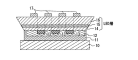
以下、本発明の実施例について図面を参照しつつ説明する。図1は、本発明の第1の実施例による半導体発光素子100の断面を示す断面図である。図1に示すように、かかる半導体発光素子は、支持基板10上に、キャップ電極11、反射電極12、p電極膜13、p−GaN(窒化ガリウム)層14、発光層15、n−GaN層16及びn電極17を積層させた構造を有する。この際、p−GaN層14、発光層15及びn−GaN層16が積層された構造体がLED層19となる。
Embodiments of the present invention will be described below with reference to the drawings. FIG. 1 is a cross-sectional view showing a cross section of a semiconductor
支持基板10は、例えば熱伝導率60W/mK又は150W/mKのSi(シリコン)からなる。尚、支持基板10としては、熱伝導率160W/mKのCuW(銅タングステン)、熱伝導率17W/mKのAlN(窒化アルミ)、熱伝導率300W/mKのSiC(炭化シリコン)、又は熱伝導率400W/mKのCu(銅)等を用いるようにしても良い。
The
キャップ電極11は、支持基板10上に形成されており、例えばTi(チタン)/Pt(プラチナ)/Au(金)、或いはTiW(チタンタングステン)/Ti/Pt/Auのような金属が積層されてなる膜厚が約500μm以上の電極膜である。
The
反射電極12は、キャップ電極11上に形成されており、例えばAg(銀)からなる膜厚が約40nm以上の電極膜である。尚、反射電極12は、発光層15から放出された光を反射させる為に設けられているものである。この際、高い反射率を得る為には、反射電極12の厚さが50nm以上であることが望ましい。
The
p電極膜13は、反射電極12及びp−GaN層14に挟まれて形成されており、例えばITO(Indium Tin Oxide)又はIZO(Indium Zinc Oxide)等からなる、膜厚が約5nm〜50nmの透明導電性の金属酸化膜である。p電極膜13には、このp電極膜13の材料であるITO又はIZO自体の抵抗値を有する低抵抗領域LRと、低抵抗領域LRよりも抵抗値が高い高抵抗領域HRとが、図1に示すように、LED層19とp電極膜13との界面に沿って形成されている。この際、これら高抵抗領域HR及び低抵抗領域LRは、p電極膜13内において、LED層19を介した高抵抗領域HR及びn電極17間の距離が、LED層19を介した低抵抗領域LR及びn電極17間の距離よりも小となる位置に夫々形成されている。尚、高抵抗領域HRは、低抵抗領域LRよりも高い酸素濃度を有し、これにより低抵抗領域LRよりも抵抗値が高くなっている。
The p-
p−GaN層14は、p電極膜13上に形成されており、例えばMg(マグネシウム)のようなp型ドーパントが添加された、膜厚が約0.05μm〜0.03μmのp型のGaN系半導体結晶膜からなる半導体層である。発光層15は、InGaN(インジウム窒化ガリウム)結晶からなる井戸層と、この井戸層よりもIn組成(X)の小さいInXGa(1-X)N結晶又はGaN結晶からなる障壁層とが交互に繰り返し積層されてなる、いわゆる多重量子井戸構造(MQW:Multiple Quantum Well)からなる。尚、井戸層及び障壁層の各々の層厚は、約3nm〜10nmである。n−GaN層16は、発光層15上に形成されており、例えばSi(シリコン)のようなn型ドーパントが添加された、膜厚が約3μm〜7μmのn型のGaN系半導体結晶膜からなる半導体層である。尚、n−GaN層16における発光層14との界面に対向する面が、発光層15からの放出光を外部に取り出す光取出面となる。
The p-
上記したp−GaN層14、発光層15及びn−GaN層16が積層された構造体が、発光ダイオードとしてのLED層19となる。
The structure in which the p-
n電極17は、n−GaN層16の表面、つまり光取出面の一部を覆うように形成された、例えばTi/Al/Pt/Au又はTi/Ni/Auのような金属が積層されてなる電極片である。尚、n電極17は、図1に示すように、n−GaN層16上における、p電極膜13の高抵抗領域HRに対向した位置に形成されている。
The
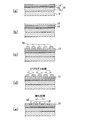
図2は、上記した半導体発光素子を製造する際の製造手順を示すフロー図である。先ず、有機金属気相成長(以下、MOCVDと称する)法により、図3(a)に示すように、サファイア等からなる成長基板9上に、上記したn−GaN層16、発光層15及びp−GaN層14が順に積層されてなるLED層を形成する(LED層形成工程S1)。
FIG. 2 is a flowchart showing a manufacturing procedure when manufacturing the semiconductor light emitting device described above. First, as shown in FIG. 3A, by the metal organic chemical vapor deposition (hereinafter referred to as MOCVD) method, on the
次に、スパッタ又はEB(電子ビーム)蒸着により、図3(b)に示すように、p−GaN層14上に、膜厚が約5nm〜30nmのITO又はIZO等の透明導電性の金属酸化膜からなるp電極膜13を形成する(p電極形成工程S2)。
Next, by sputtering or EB (electron beam) deposition, as shown in FIG. 3B, a transparent conductive metal oxide such as ITO or IZO having a film thickness of about 5 nm to 30 nm is formed on the p-
次に、図3(c)に示すように、p電極膜13上における低抵抗領域LRの形成予定箇所にレジストRgをパターンニングし、引き続き、図3(d)に示すように、レジストRgを隔ててp電極膜13に対して、例えば1.0Paの圧力、処理時間1分の条件で酸素プラズマ処理を施す。
Next, as shown in FIG. 3C, a resist Rg is patterned at a location where the low resistance region LR is to be formed on the p-
かかる酸素プラズマ処理によれば、p電極膜13における、レジストRgに覆われていない領域が酸素プラズマに曝され、その領域内に酸素が取り込まれる。これにより、p電極膜13における、レジストRgに覆われていない領域内の酸素濃度が増加し、高抵抗化する。その後、図3(e)に示すように、レジストRgを除去した状態でp電極膜13の表面に酸化処理を施すことにより、p電極膜13の透過率を高める。例えばp電極膜13の表面に対して、例えばRTA(急速加熱)装置を用い、酸素雰囲気下で、400℃〜600℃の処理温度による1分〜10分間のアニール(熱処理)を施すことにより、p電極膜13の表面の酸素濃度を高める。
According to such oxygen plasma treatment, a region of the p-
かかる酸化処理によれば、p電極膜13中の酸素プラズマに曝された領域において酸素原子が結晶格子に取り込まれ、この領域の抵抗値が更に高まる。よって、上記した酸素プラズマ処理及び酸化処理により、このp電極膜13として用いられる材料の抵抗値(例えば、ITOの接触抵抗10-4オーム)の低抵抗領域LR及びその抵抗値の約5〜30倍程度の抵抗値を有する高抵抗領域HRが、図3(e)に示すように、LED層19とp電極膜13との界面に沿って交互に形成される(高抵抗化工程S3)。
According to such oxidation treatment, oxygen atoms are taken into the crystal lattice in the region of the p-
図3(e)に示す酸化処理の実行後、図4(a)に示すように、p電極膜13を各素子毎の形態にパターンニングし、引き続きスパッタ又はEB蒸着により、p電極膜13上に、Agからなる膜厚が約50nm以上の反射電極12を形成する(反射電極形成工程S4)。
After execution of the oxidation treatment shown in FIG. 3 (e), as shown in FIG. 4 (a), the p-
次に、スパッタ又はEB蒸着により、図4(a)に示すように、かかる反射電極12上にTi/Pt/Auのような金属が積層されてなる、膜厚が約500μm以上のキャップ電極11を形成する(キャップ電極形成工程S5)。この際、キャップ電極11の一方の界面、つまり反射電極12との接合面はTiで形成されており、他方の界面、つまり支持基板10との接合面はAuで形成されている。尚、反射電極12、つまりAg(銀)のマイグレーションを防止する為には、キャップ電極11の材料としては、例えばTiW(チタンタングステン)のようなバリアメタルを含む合金、例えばTiW(チタンタングステン)/Ti/Pt/Auが積層されてなる合金を用いるのが望ましい。
Next, as shown in FIG. 4A, a
次に、ドライエッチング処理を施すことによりLED層19を素子毎に分割し、引き続き、この分割したキャップ電極11に、図4(b)に示すように支持基板10を貼り合わせる(支持基板貼合工程S6)。支持基板10の表面にはAu(金)膜(図示せず)が形成されており、支持基板貼合工程S6では、キャップ電極11の表面と支持基板10の表面とを、Au/Au接合によるウェハボンディングによって貼り合わせる。尚、キャップ電極11に支持基板10を貼り合わせる方法としては、上記のような金属同士の接合のみならず、金属共晶接合を用いても良い。この際、支持基板10の表面にはAu(金)に代えて例えばSn(スズ)を形成しておき、支持基板10の表面とキャップ電極11とを接合する(Sn/Au接合)。
Next, the
尚、図3(a)〜図3(e)及び図4(a)はウェハ中の一部の断面構造を示すものであり、図4(b)及び以下の図4(c)及び図4(d)は、このウェハから分割した1発光素子分の断面構造を示すものである。 3 (a) to 3 (e) and 4 (a) show a partial cross-sectional structure in the wafer. FIG. 4 (b) and FIGS. (D) shows a cross-sectional structure of one light emitting element divided from the wafer.
上記した支持基板貼合工程S6の終了後、レーザリフトオフ法により、図4(c)に示すように、n−GaN層16から成長基板9を剥がしてこれを除去する(成長基板除去工程S7)。
After completion of the support substrate bonding step S6 described above, the
次に、スパッタ又はEB蒸着により、n−GaN層16上におけるp電極膜13の高抵抗領域HRに対向した位置に、Ti/Al/Pt/Au又はTi/Ni/Auのような電極膜からなるn電極17を、図4(d)に示すように形成する。すなわち、LED層19を介した高抵抗領域HR及びn電極17間の電流経路が、LED層19を介した低抵抗領域LR及びn電極17間の電流経路よりも短くなるようなn−GaN層16上の位置に、n電極17を形成するのである(n電極形成工程S8)。
Next, an electrode film such as Ti / Al / Pt / Au or Ti / Ni / Au is formed on the n-
尚、高抵抗領域HRは、これをn−GaN層16の上方から平面視で眺めたときに、n電極17以上の大きさを有し且つn電極17が高抵抗領域HR内に納まるような位置に形成することが好ましい。
The high resistance region HR has a size larger than that of the
以上のように、図1に示される半導体発光素子100では、p−GaN層14の表面を覆うp電極膜13として、LED層19とp電極膜13との界面に沿って、互いに抵抗値が異なる低抵抗領域LR及び高抵抗領域HRが交互に形成されている電極膜を採用する。この際、p電極膜13の高抵抗領域HRは、n−GaN層16の表面の一部を覆うn電極17に対向した位置に形成されている。すなわち、図5に示すように、p電極膜13内において、LED層19を介した高抵抗領域HR及びn電極17間の電流経路L2が、LED層19を介した低抵抗領域LR及びn電極17間の電流経路L1よりも短くなる位置に、高抵抗領域HR及び低抵抗領域LRを夫々形成したのである。
As described above, in the semiconductor
かかる構成によれば、p電極膜13の低抵抗領域LRからは、LED層19内の電流経路L1(一点鎖線にて示す)を介してn電極17側に駆動電流が流れる。また、p電極膜13の高抵抗領域HRからは、LED層内の電流経路L2を介してn電極17側に駆動電流が流れる。この際、図5に示すように、p電極膜13の高抵抗領域HRはLED層を挟んでn電極17に対向した位置に存在し、p電極膜13の低抵抗領域LRはn電極17に対向した位置からずれた位置に存在するので、電流経路L2の経路長は電流経路L1の経路長よりも短くなる。つまり、p電極膜13の高抵抗領域HR及びn電極17間に形成される電流経路L2での抵抗値は、p電極膜13の低抵抗領域LR及びn電極17間に形成される電流経路L1での抵抗値よりも低くなる。ところが、p電極膜13における高抵抗領域HRは低抵抗領域LRよりも抵抗値が高いので、電流経路L2に多くの電流が集中することを防止し、電流経路L1にも電流が広がるようにすることが可能となる。
According to such a configuration, a drive current flows from the low resistance region LR of the
従って、図1に示す半導体発光素子100によれば、LED層19の広い範囲に駆動電流を流すことができるようになり、発光効率を改善することが可能となる。
Therefore, according to the semiconductor
このとき、抵抗値によって電流経路L1と電流経路L2に流れる電流値の差を小さくすることも可能であるが、電流経路L2よりも電流経路L1に流れる電流値を大きくすることもできる。このような場合であっても電流を広範囲に広げる効果は同様に発揮される為、発光効率の改善に繋がる。また、図1のように光を透過させない電極が発光面にある場合、電極真下の発光は電極に阻害され、光を取り出すことが出来ない。そのため、電極直下から外れるような電流経路L1に電流がより多く流れた方が、より高効率な発光を実現できる。 At this time, the difference between the current values flowing in the current path L1 and the current path L2 can be reduced by the resistance value, but the current value flowing in the current path L1 can be made larger than the current path L2. Even in such a case, the effect of spreading the current over a wide range is exhibited in the same manner, which leads to an improvement in luminous efficiency. In addition, when an electrode that does not transmit light is present on the light emitting surface as shown in FIG. 1, light emission directly under the electrode is inhibited by the electrode, and light cannot be extracted. Therefore, more efficient light emission can be realized when a larger amount of current flows through the current path L1 that is off from directly below the electrode.
また、図1に示す半導体発光素子100では、前述したように、p電極膜13の一部の領域(HR)を高抵抗化することにより、LED層内に流れる駆動電流の均一化を図るようにしている。これにより、LED層内に流れる駆動電流を広げる為にこのLED層に含まれるGaN系半導体層の一部の領域をプラズマ処理によって高抵抗化する場合に生じる、以下の問題が回避される。すなわち、従来、GaN系半導体層の一部の領域を高抵抗化する為には、GaN系半導体層に対して、レジストのパターンニング、不活性ガスによるプラズマ処理、及びレジスト除去処理を実施することになる。しかしながら、そのレジスト除去処理において、GaN系半導体層の表面に塗布するレジスト剥離剤及び洗浄剤により、GaN系半導体層の表面状態が悪化、つまりその後の工程で電極膜を表面に成膜することが出来なくなるような表面状態に悪化する場合があった。
In the semiconductor
この際、図1に示す半導体発光素子100では、GaN系半導体層(14)の表面に対しては、その表面状態を悪化させるようなレジスト除去処理が為されないので、このGaN系半導体層の表面に電極膜を良好に成膜することが可能となる。
At this time, in the semiconductor
よって、本発明に係る半導体発光素子によれば、歩留まりを低下させることなく、光放出面内での発光強度の分布を均一化することが可能となる。 Therefore, according to the semiconductor light emitting device of the present invention, it is possible to make the light emission intensity distribution uniform within the light emitting surface without reducing the yield.
尚、本発明では、LED層内に流れる駆動電流の拡散を図るという目的を達成すべく、p電極膜13として、高抵抗領域HR及び低抵抗領域LRを有するものを採用している。しかしながら、同様な目的を達成する為に、図6に示すように、p−GaN層14上におけるn電極17に対向した領域以外の領域にp電極膜13をパターンニングすることも考えられる。この際、p−GaN層14上にp電極膜13をパターンニングする為に、図3(a)〜図3(c)に示す一連の工程終了後、引き続き図7(a)に示すように、p電極膜13に対してエッチング処理を施す。かかるエッチング処理により、p電極膜13においてレジストRgに覆われていない箇所が除去される。しかしながら、その除去が完全に為されない場合があり、この際、図7(b)に示すような電極残渣PZがp−GaN層14上に残留する。次に、レジスト剥離剤及び洗浄剤により、図7(b)に示すようなレジストRgを除去すべきレジスト除去処理を行う。しかしながら、その除去が完全になされない場合があり、この際、図7(c)に示すようなレジスト残渣EZがp電極膜13上に残留する。その後、図7(c)に示すように、p電極膜13及びp−GaN層14上に、Ag(銀)からなる反射電極12が成膜される。ところが、上記したエッチング処理で使用されたエッチング液及びレジスト除去処理で使用されたレジスト剥離剤及び洗浄剤によってp−GaN層14の表面状態が悪化している為、p−GaN層14及び反射電極12の界面で図7(c)に示すようなAg(銀)の凝集GSが生じる場合があった。
In the present invention, in order to achieve the purpose of diffusing the drive current flowing in the LED layer, the
従って、図6に示すような、p電極膜13をパターンニングした構造を採用した場合には、図7(c)に示すように反射電極12内に残留する電極残渣PZ、並びに、p−GaN層14及び反射電極12の界面で生じているAgの凝集GSにより、反射電極12での反射率が低下するという問題があった。
Accordingly, when a structure in which the p-
しかしながら、本発明に係る半導体発光素子では、p電極膜13に対してエッチング処理を実施することはないので、電極残渣PZの残留、及びAgの凝集GSが生じる虞が無い。よって、本発明によれば、電極残渣PZ及びAgの凝集GSに起因する、反射電極12の反射率低下が生じないので、高効率な発光を実現することが可能となる。
However, in the semiconductor light emitting device according to the present invention, the etching process is not performed on the p-
また、上記した実施例では、半導体発光素子として、図1に示すような薄膜フィルム構造を有するものを例にとって説明したが、フリップ・チップ構造の素子にも適用することが可能である、
図8は、かかる点に鑑みて為された、フリップ・チップ構造からなる本発明の第2の実施例による半導体発光素子200の構成を示す断面図である。
In the above-described embodiment, the semiconductor light emitting device has been described by taking the thin film film structure as shown in FIG. 1 as an example, but it can also be applied to a flip chip structure device.
FIG. 8 is a cross-sectional view showing the configuration of the semiconductor
図8に示す半導体発光素子200においては、キャップ電極11、反射電極12、p電極膜13、p−GaN層14、発光層15及びn−GaN層16を積層した構造を有する点については、図1に示す半導体発光素子100と同一である。ただし、半導体発光素子200LED層19は、図8に示すように、p−GaN層14及び発光層15を貫通してn−GaN層16の表面を露出させる凹部を有する。そして、n−GaN層16の凹部からの露出面に、Ti/Al/Ti/Pt/Auからなる柱状のn電極20の一端が直接接続されている。この際、n電極20の他端は、ボンディングメタル21Aを介して、例えばPCB(printed circuit board)からなる基板50に配線されている第1のライン(図示せぬ)に接続されており、キャップ電極11はボンディングメタル21Bを介して、基板50に配線されている第2のライン(図示せぬ)に接続されている。また、この半導体発光素子200に形成されているp電極膜13では、n電極20に最も近い領域が上述した高抵抗領域HRとなっており、n電極20の一端から離れている領域が低抵抗領域LRとなっている。すなわち、図5の場合と同様に、p電極膜13内においてn電極20から離れた位置の領域ほどLED層19内での電流経路が長くなりその抵抗値が高くなるので、p電極膜13内においてn電極20に最も近い位置に存在する領域を高抵抗化することにより、LED層内に流れる駆動電流の拡散を図るのである。尚、図8に示す一例では、LED層を形成させる為の成長基板9がLED層に付着したままとなっているが、これを剥がすようにしても良い。
The semiconductor
要するに、本発明に係る半導体発光素子は、第1の半導体層であるp−GaN層14、発光層15及び第2の半導体層であるn−GaN層16が積層されてなるLED層19と、第1の半導体層上に形成された第1電極としてのp電極膜13と、第2の半導体層上に形成された第2電極としてのn電極17(20)と、を有するものである。ここで、第1電極には、LED層と第1電極との界面に沿って、互いに抵抗値が異なる低抵抗領域(LR)及び高抵抗領域(HR)が形成されている。この際、これら高抵抗領域及び低抵抗領域は、LED層を介した高抵抗領域及び第2電極間の電流経路が、LED層を介した低抵抗領域及び第2電極間の電流経路よりも短くなる位置に夫々形成されているのである。
In short, the semiconductor light emitting device according to the present invention includes an
尚、第1の半導体層をp型の半導体層、第2の半導体層をn型の半導体層として説明しているが、第1の半導体層がn型の半導体層、第2の半導体層がp型の半導体層であっても良い。要するに、LED層としては、第1導電型の第1の半導体層、発光層、及び第1導電型とは反対導電型の第2導電型の第2の半導体層が積層された構造を有するものであれば良いのである。 Although the first semiconductor layer is described as a p-type semiconductor layer and the second semiconductor layer is described as an n-type semiconductor layer, the first semiconductor layer is an n-type semiconductor layer, and the second semiconductor layer is It may be a p-type semiconductor layer. In short, the LED layer has a structure in which a first conductivity type first semiconductor layer, a light emitting layer, and a second conductivity type second semiconductor layer opposite to the first conductivity type are stacked. If it is good.
12 反射電極
13 p電極膜
14 p−GaN層
15 発光層
16 n−GaN層
17 n電極
100、200 半導体発光素子
DESCRIPTION OF
Claims (6)
前記第1電極には、前記LED層と前記第1電極との界面に沿って、互いに抵抗値が異なる低抵抗領域及び高抵抗領域が形成されており、
前記第1電極内において、前記LED層を介した前記高抵抗領域及び前記第2電極間の電流経路が前記LED層を介した前記低抵抗領域及び前記第2電極間の電流経路よりも短くなる位置に、前記高抵抗領域及び低抵抗領域が夫々形成されていることを特徴とする半導体発光素子。 An LED layer in which a first semiconductor layer of a first conductivity type, a light emitting layer, and a second semiconductor layer of a second conductivity type opposite to the first conductivity type are stacked, and the first semiconductor layer A first electrode formed on the second semiconductor layer, and a second electrode formed on the second semiconductor layer,
A low resistance region and a high resistance region having different resistance values are formed along the interface between the LED layer and the first electrode in the first electrode.
In the first electrode, a current path between the high resistance region and the second electrode via the LED layer is shorter than a current path between the low resistance region and the second electrode via the LED layer. The semiconductor light emitting element, wherein the high resistance region and the low resistance region are formed at positions.
前記第2電極は、前記第2の半導体層の前記凹部からの露出面に形成されていることを特徴とする請求項1記載の半導体発光素子。 The LED layer has a recess that penetrates the first semiconductor layer and the light emitting layer and exposes a surface of the second semiconductor layer;
2. The semiconductor light emitting element according to claim 1, wherein the second electrode is formed on an exposed surface of the second semiconductor layer from the recess.
前記第1の半導体層上に第1電極を形成する第1電極形成工程と、
前記第2の半導体層上に第2電極を形成する第2電極形成工程と、
前記第1電極上にパターンニングしたレジストを形成し、前記レジストをマスクとして前記第1電極に酸素プラズマ処理を施すことにより、前記第1電極の一部を高抵抗化した高抵抗領域と、前記高抵抗領域よりも抵抗値が低い低抵抗領域とを、前記LED層と前記第1電極との界面に沿って交互に形成する高抵抗化工程と、を有し、
前記第2電極形成工程では、前記LED層を介した前記高抵抗領域及び前記第2電極間の電流経路が、前記LED層を介した前記低抵抗領域及び前記第2電極間の電流経路よりも短くなるような前記第2の半導体層上の位置に前記第2電極を形成することを特徴とする半導体発光素子の製造方法。 An LED layer forming step of forming an LED layer in which a first semiconductor layer of a first conductivity type, a light emitting layer, and a second semiconductor layer of a second conductivity type opposite to the first conductivity type are stacked;
A first electrode forming step of forming a first electrode on the first semiconductor layer;
A second electrode forming step of forming a second electrode on the second semiconductor layer;
Forming a patterned resist on the first electrode, and subjecting the first electrode to an oxygen plasma treatment using the resist as a mask; A high resistance step of alternately forming a low resistance region having a resistance value lower than that of the high resistance region along the interface between the LED layer and the first electrode,
In the second electrode forming step, the current path between the high resistance region and the second electrode via the LED layer is more than the current path between the low resistance region and the second electrode via the LED layer. A method of manufacturing a semiconductor light emitting element, wherein the second electrode is formed at a position on the second semiconductor layer so as to be shortened.
Priority Applications (1)
| Application Number | Priority Date | Filing Date | Title |
|---|---|---|---|
| JP2013044002A JP2014175338A (en) | 2013-03-06 | 2013-03-06 | Semiconductor light-emitting element and manufacturing method of the same |
Applications Claiming Priority (1)
| Application Number | Priority Date | Filing Date | Title |
|---|---|---|---|
| JP2013044002A JP2014175338A (en) | 2013-03-06 | 2013-03-06 | Semiconductor light-emitting element and manufacturing method of the same |
Publications (1)
| Publication Number | Publication Date |
|---|---|
| JP2014175338A true JP2014175338A (en) | 2014-09-22 |
Family
ID=51696320
Family Applications (1)
| Application Number | Title | Priority Date | Filing Date |
|---|---|---|---|
| JP2013044002A Pending JP2014175338A (en) | 2013-03-06 | 2013-03-06 | Semiconductor light-emitting element and manufacturing method of the same |
Country Status (1)
| Country | Link |
|---|---|
| JP (1) | JP2014175338A (en) |
Cited By (3)
| Publication number | Priority date | Publication date | Assignee | Title |
|---|---|---|---|---|
| JP2016115920A (en) * | 2014-12-15 | 2016-06-23 | 豊田合成株式会社 | Light-emitting element |
| WO2016208963A1 (en) * | 2015-06-23 | 2016-12-29 | 고려대학교 산학협력단 | Transparent electrode and method for forming transparent electrode |
| JP2021158179A (en) * | 2020-03-26 | 2021-10-07 | 豊田合成株式会社 | Light-emitting device |
Citations (4)
| Publication number | Priority date | Publication date | Assignee | Title |
|---|---|---|---|---|
| JPS5772235A (en) * | 1980-10-20 | 1982-05-06 | Matsushita Electric Ind Co Ltd | Transparent electrode and production thereof |
| JP2010080542A (en) * | 2008-09-24 | 2010-04-08 | Toyoda Gosei Co Ltd | Group iii nitride semiconductor light-emitting element and method for manufacturing the same |
| WO2011033625A1 (en) * | 2009-09-16 | 2011-03-24 | 株式会社 東芝 | Semiconductor light emitting element |
| JP2011129922A (en) * | 2009-12-21 | 2011-06-30 | Lg Innotek Co Ltd | Light emitting element, light emitting element manufacturing method, light emitting element package, and lighting system |
-
2013
- 2013-03-06 JP JP2013044002A patent/JP2014175338A/en active Pending
Patent Citations (4)
| Publication number | Priority date | Publication date | Assignee | Title |
|---|---|---|---|---|
| JPS5772235A (en) * | 1980-10-20 | 1982-05-06 | Matsushita Electric Ind Co Ltd | Transparent electrode and production thereof |
| JP2010080542A (en) * | 2008-09-24 | 2010-04-08 | Toyoda Gosei Co Ltd | Group iii nitride semiconductor light-emitting element and method for manufacturing the same |
| WO2011033625A1 (en) * | 2009-09-16 | 2011-03-24 | 株式会社 東芝 | Semiconductor light emitting element |
| JP2011129922A (en) * | 2009-12-21 | 2011-06-30 | Lg Innotek Co Ltd | Light emitting element, light emitting element manufacturing method, light emitting element package, and lighting system |
Cited By (5)
| Publication number | Priority date | Publication date | Assignee | Title |
|---|---|---|---|---|
| JP2016115920A (en) * | 2014-12-15 | 2016-06-23 | 豊田合成株式会社 | Light-emitting element |
| WO2016208963A1 (en) * | 2015-06-23 | 2016-12-29 | 고려대학교 산학협력단 | Transparent electrode and method for forming transparent electrode |
| JP2021158179A (en) * | 2020-03-26 | 2021-10-07 | 豊田合成株式会社 | Light-emitting device |
| JP7283428B2 (en) | 2020-03-26 | 2023-05-30 | 豊田合成株式会社 | light emitting device |
| US11764329B2 (en) | 2020-03-26 | 2023-09-19 | Toyoda Gosei Co., Ltd. | Light emitting device |
Similar Documents
| Publication | Publication Date | Title |
|---|---|---|
| JP4999696B2 (en) | GaN-based compound semiconductor light emitting device and manufacturing method thereof | |
| JP2008227109A (en) | GaN-BASED LED ELEMENT AND LIGHT-EMITTING DEVICE | |
| KR100999726B1 (en) | Light emitting device and method for fabricating the same | |
| JP2007287757A (en) | Nitride semiconductor light-emitting element and its manufacturing method | |
| JP2007103690A (en) | Semiconductor light emitting device and its fabrication process | |
| US20040201110A1 (en) | Flip-chip light emitting diode with indium-tin-oxide based reflecting contacts | |
| JP2005117020A (en) | Gallium nitride based compound semiconductor device and its manufacturing method | |
| JP5326957B2 (en) | Light emitting device manufacturing method and light emitting device | |
| JP2005197631A (en) | Method of manufacturing gallium-nitride-based semiconductor light-emitting element | |
| JP2005340860A (en) | Semiconductor light-emitting element | |
| JP2012186199A (en) | Semiconductor light-emitting device and method of manufacturing the same | |
| JP5471485B2 (en) | Nitride semiconductor device and pad electrode manufacturing method for nitride semiconductor device | |
| JP2007207869A (en) | Nitride semiconductor light-emitting device | |
| JP4386185B2 (en) | Nitride semiconductor device | |
| JP2014175338A (en) | Semiconductor light-emitting element and manufacturing method of the same | |
| JP5221166B2 (en) | ZnO-based semiconductor element, manufacturing method thereof, and optical semiconductor element | |
| JP2007149983A (en) | Manufacture of nitride semiconductor light-emitting element | |
| KR101239852B1 (en) | GaN compound semiconductor light emitting element | |
| TWI505502B (en) | Light-emitting diode and method for manufacturing thereof | |
| JP4622426B2 (en) | Semiconductor light emitting device | |
| JP5945409B2 (en) | Semiconductor device and manufacturing method thereof | |
| KR101534846B1 (en) | fabrication of vertical structured light emitting diodes using group 3 nitride-based semiconductors and its related methods | |
| JP2008226866A (en) | Gallium nitride based light-emitting diode element and light-emitting device | |
| JP2014165337A (en) | Light-emitting element, light-emitting element package, and method of manufacturing light-emitting element | |
| JP5098482B2 (en) | LIGHT EMITTING DEVICE MANUFACTURING METHOD AND LIGHT EMITTING DEVICE |
Legal Events
| Date | Code | Title | Description |
|---|---|---|---|
| A621 | Written request for application examination |
Free format text: JAPANESE INTERMEDIATE CODE: A621 Effective date: 20160209 |
|
| A977 | Report on retrieval |
Free format text: JAPANESE INTERMEDIATE CODE: A971007 Effective date: 20161026 |
|
| A131 | Notification of reasons for refusal |
Free format text: JAPANESE INTERMEDIATE CODE: A131 Effective date: 20161108 |
|
| A02 | Decision of refusal |
Free format text: JAPANESE INTERMEDIATE CODE: A02 Effective date: 20170502 |