JP2014142379A - Planar display device - Google Patents
Planar display device Download PDFInfo
- Publication number
- JP2014142379A JP2014142379A JP2013008964A JP2013008964A JP2014142379A JP 2014142379 A JP2014142379 A JP 2014142379A JP 2013008964 A JP2013008964 A JP 2013008964A JP 2013008964 A JP2013008964 A JP 2013008964A JP 2014142379 A JP2014142379 A JP 2014142379A
- Authority
- JP
- Japan
- Prior art keywords
- double
- display panel
- adhesive tape
- flat display
- tape member
- Prior art date
- Legal status (The legal status is an assumption and is not a legal conclusion. Google has not performed a legal analysis and makes no representation as to the accuracy of the status listed.)
- Pending
Links
Images


Abstract
Description
本発明は、液晶表示装置や有機EL表示装置、プラズマディスプレイなどの平面表示装置において、平面表示パネルとベゼルまたは面光源装置などの被接着部材とを接着する両面接着テープを改良した平面表示装置に関する。 The present invention relates to a flat display device in which a double-sided adhesive tape for bonding a flat display panel and a member to be bonded such as a bezel or a surface light source device is improved in a flat display device such as a liquid crystal display device, an organic EL display device, or a plasma display. .
現在、平面表示装置は薄型軽量化や低消費電力などの点からカラーテレビやパーソナルコンピュータ及び映像表示用モニターや携帯電話などに広く採用されている。このような平面表示装置においては、平面表示パネルを主体として、この平面表示パネルと当該平面表示パネルの前面に配置されるベゼルとの間、もしくは平面表示パネルと当該平面表示パネルを裏面から照射する面光源装置との間を両面接着テープによって接着し固定する構成が採用されており、この両面接着テープを用いた平面表示装置が特許文献1に記載されている。 Currently, flat display devices are widely used in color televisions, personal computers, video display monitors, mobile phones, and the like in terms of thinness and weight reduction and low power consumption. In such a flat display device, the flat display panel is mainly used, and the flat display panel and the flat display panel are irradiated from the back surface or between the flat display panel and the bezel arranged in front of the flat display panel. A configuration is adopted in which a surface light source device is bonded and fixed with a double-sided adhesive tape, and a flat display device using this double-sided adhesive tape is described in Patent Document 1.
このように平面表示パネルとベゼルとの間、もしくは平面表示パネルと面光源装置との間を隙間なく両面接着テープによって接着固定することによって、平面表示装置の内部に外部からの塵埃などが侵入しないように抑制している。 In this way, by adhering and fixing the flat display panel and the bezel or between the flat display panel and the surface light source device with a double-sided adhesive tape without any gap, dust from the outside does not enter the flat display device. Is suppressed.
しかしながら、この両面接着テープを使用して隙間なく両者を接着させるための構成が複雑化しており、また、接着作業にも多くの手間が掛かるという問題がある。 However, the structure for adhering both without any gap using this double-sided adhesive tape is complicated, and there is a problem that much work is required for the bonding operation.
実施形態の解決しようとする課題は、簡単な構成ながら隙間をなくし、もしくは隙間をより狭くなるように構成することにより、外部からの塵埃の侵入を阻止することが可能であり、且つ、作業性にも優れた平面表示装置を提供することにある。 The problem to be solved by the embodiment is that it is possible to prevent the intrusion of dust from the outside by eliminating the gap or making the gap narrower with a simple configuration, and workability It is another object of the present invention to provide an excellent flat display device.
実施形態の平面表示装置は、対向する一対の基板を有する平面表示パネルと、この平面表示パネルと被接着体とを接着する平面視矩形枠状の両面接着テープと、を備える平面表示装置において、両面接着テープは、複数のテープ部材片の組合せから構成され、前記テープ部材片の夫々の端部には薄肉部が形成され、隣接するテープ部材片端部に形成された薄肉部同士が重畳するように重ねられて接着されていることを特徴とする平面表示装置である。 A flat display device according to an embodiment includes a flat display panel having a pair of opposing substrates, and a double-sided adhesive tape having a rectangular frame shape in a plan view for bonding the flat display panel and an adherend, The double-sided adhesive tape is composed of a combination of a plurality of tape member pieces, and a thin wall portion is formed at each end portion of the tape member piece, and the thin wall portions formed at the adjacent tape member piece end portions overlap each other. The flat display device is characterized in that it is superposed on and adhered to the flat display device.
以下、図面を参照して実施形態に係る平面表示装置について詳細に説明する。 Hereinafter, a flat display device according to an embodiment will be described in detail with reference to the drawings.
実施形態の平面表示装置として、平面表示パネルに液晶表示パネルを採用した液晶表示装置に適用した場合について説明する。 A case where the present invention is applied to a liquid crystal display device employing a liquid crystal display panel as a flat display panel will be described as the flat display device of the embodiment.
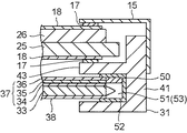
この液晶表示装置は、図1及び図4に示すように、表示領域10と、この表示領域10の外周に形成される額縁領域(非表示領域)11を備えた液晶表示パネル12を有し、この液晶表示パネル12の前面(視認側)に、表示領域10に対向する部分に開口部13を有し、額縁領域11に対向する部分に本体部14を有するベゼル(被接着体)15が配置されている。
As shown in FIGS. 1 and 4, the liquid crystal display device includes a liquid
一方、液晶表示パネル12の背面側(非視認側)には、面光源装置(被接着体)16が配置されている。
On the other hand, a surface light source device (adhered body) 16 is disposed on the back side (non-viewing side) of the liquid
そして、これら液晶表示パネル12とベゼル15との間、即ち、額縁領域11と本体部14裏面との間、及び液晶表示パネル12の額縁領域11と面光源装置16との非照射領域との間には、夫々平面視矩形枠状の両面接着テープ17が介在されており、この両面接着テープ17によって、夫々液晶表示パネル12とベゼル15間、及び液晶表示パネル12と面光源装置16との間を接着固定している。
And between the liquid
この液晶表示パネル12は、ガラス材や合成樹脂材から構成される透明絶縁基板19の主面上に、酸化インジウムスズ(ITO)などからなる表示画素20を構成する透明画素電極21がマトリクス状に配置されており、これら画素電極21の行方向には複数の走査線22が、また画素電極21の列方向には複数本の信号線23が配設されている。
In this liquid
この画素電極21に対応して、走査線22及び信号線23の交差位置近傍には、スイッチング素子としての複数のTFT24が配設されている。このTFT24は、画素電極21の行方向に沿って形成される走査線22とゲート電極が接続され、また画素電極21の列方向に沿って形成される信号線23にソース電極もしくはドレイン電極が接続されており、走査線駆動回路(図示せず)から走査線22を介して供給される駆動電圧によってTFT24が導通し、信号線駆動回路(図示せず)からの信号電圧をTFT24のソース・ドレイン通路を通して画素電極21に印加するように動作する。
Corresponding to the
この画素電極21には、所定の電位に設定された補助容量線から構成される補助容量(図示せず)が並列に接続されており、これらTFT24や画素電極21、走査線22や信号線23などの駆動線の上面には、さらにポリイミドなどから構成される配向膜(図示せず)が設けられて、アレイ基板25が構成されている。
The
また、このアレイ基板25と対向する対向基板26は、同様にガラス材や合成樹脂材にて形成された透明絶縁基板27と、この透明絶縁基板27のアレイ基板25と対向する主面上には、その周辺部分に黒色の遮光膜(図示せず)が設けられるとともに、ITOなどから構成される透明共通電極28が設けられ、この共通電極28の上面には、さらにポリイミドなどからなる配向膜(図示せず)が設けられている。
Further, the
この遮光膜に囲まれた絶縁基板27部分には,アクリル材などから構成される三原色カラーフィルタ(図示せず)、並びに配線間の隙間からの漏光を遮断するためのブラックマトリクス(図示せず)が設けられて対向基板26を構成している。これら共通電極28には共通電極駆動回路(図示せず)からの駆動電圧が供給されている。
The
このアレイ基板25と対向基板26は,所定の間隙を持って対向配置されるとともにシール材(図示せず)を介して貼り合わされており、この間隙部には液晶部材29が封止されている。この液晶部材29の厚さは、アレイ基板25と対向基板26間に介在されるスペーサ(図示せず)によって規定されて,液晶表示パネル12が構成されている。この液晶表示パネル12の両外表面上には,偏光板18(図4参照)が接着剤によって貼付されている。
The
さらに、アレイ基板25側の偏光板18の外方には、面光源装置16が配置されている。
Further, the surface
この面光源装置16は、発光部30と、この発光部30を挟持するフロントケース31及びバックケース32から構成されている。
The surface
この面光源装置16は、図2に示すような構成が採用される。
The surface
即ち、図4も参照して説明すると、一側面に配置され可撓性印刷配線板(FPC)50に搭載されたLED51及びリフレクタ52などからなる光源53からの光を導入して、主平面から面状の光として出射する平板状に構成された導光板33と、この導光板33の出射面側に順次配置された拡散シート34、レンズシート35、偏光シート36などの光学シート37を備えている。
That is, referring to FIG. 4 as well, light from a
なお、FPC50の配置位置は、図示の位置に限定されることなく、LED51の構成や仕様によって、LED51の下側やLED51の背面側に配置させることも可能である。
The arrangement position of the
一方、導光板33の非出射面側には反射シート38が配置されており、これら反射シート38、導光板33及び光学シート37は、一括して合成樹脂製のフレーム39に収容され、このフレーム39をさらにバックケース40とフロントケース41とで挟持することで面光源装置16を構成している。図1の発光部30は、フロントケース31とバックケース32とを除外した部分を総称して呼称しているに過ぎない。
On the other hand, a
この面光源装置16では、光学シート37として、拡散シート34、レンズシート35及び偏光シート36の3枚のシートで構成しているが、いずれかのシートを省略することも可能であり、また、更に別のシートを追加することも可能であって、その種類や構成には特に限定はされない。
In this surface
また、図2の構成では、フレーム39を用いて面光源装置16を構成しているが、図3に示すように、フレーム39を省略して、バックケース40とフロントケース31によって、これら導光板33や光学シート37及び反射シート38を保持するように構成することも可能である。ここでは説明の重複を避けるために、同じ構成要素には同じ符号を付すことによって、その詳細な説明は省略する。
In the configuration of FIG. 2, the surface
このように構成された面光源装置16の前面、即ち、フロントケース31の液晶表示パネル12の面側には、平面視で矩形枠状の両面接着テープ17の一面側が接着されている。
One surface side of the double-sided
このフロントケース31は、図1にも示されているように、枠状の本体部41と、この本体部41から内方に突出して導光板33から放射された光を通過させるための開口部42を有する保持部43を備え、この保持部43の下面に光学シート37が当接するとともに、保持部43の上面に両面接着テープ17を介して液晶表示パネル12が載置される構成となっている。換言すると、面光源装置16と液晶表示パネル12とは、両面接着テープ17によって接着されて一体化されていることとなる。
As shown in FIG. 1, the
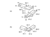
これら面光源装置16と液晶表示パネル12、並びに液晶表示パネル12とベゼル15とは、両面接着テープ17によって接着固定されている。この両面接着テープ17は、図5に示すように、長方形状で細片状の複数のテープ部材片60−1,60−2…の組合せから平面視で矩形枠状に構成される。
The surface
即ち、個々のテープ部材片60−1,60−2…は、中心に合成樹脂などから形成された基体部と、その両面に塗布されている接着剤から構成されており、そのテープ部材片60−1,60−2…の長手方向両端部分には、テープ部材片60−1,60−2…の厚さ方向の総厚に対して略半分の厚さとなるように、一方の面を基準とした薄肉部61−1,61−2…が形成されている。 That is, each of the tape member pieces 60-1, 60-2,... Is composed of a base portion formed of a synthetic resin or the like at the center and an adhesive applied to both surfaces thereof. −1, 60-2... On both sides in the longitudinal direction is based on one side so that the thickness is approximately half of the total thickness in the thickness direction of the tape member pieces 60-1, 60-2. .. Are formed.
この薄肉部61−1,61−2…は、基体部に接着剤層を形成する前の段階で基体部の端部をプレス機で押圧して厚さを薄く形成した後に接着剤層を形成するようにするか、基体部に接着剤を塗布した後に非接着性の部材でカバーされたプレス機によって押圧形成するなどの手段によって形成することが可能である。 These thin-walled portions 61-1, 61-2, ... form the adhesive layer after the thickness of the thin portion is reduced by pressing the end of the base portion with a press before forming the adhesive layer on the base portion. Alternatively, it may be formed by means such as press forming with a pressing machine covered with a non-adhesive member after applying an adhesive to the base portion.
このような薄肉部61−1,61−2…の形成は、個々のテープ部材片60−1,60−2…に分断される前段階の長尺形態の段階で行い、中間に形成された薄肉部60−1,60−2…の中心位置で切断して個々のテープ部材片60−1,60−2…を得るように構成することも可能である。 The thin-walled portions 61-1, 61-2, ... are formed in the middle of the long form before being divided into the individual tape member pieces 60-1, 60-2, and formed in the middle. It is also possible to constitute the tape member pieces 60-1, 60-2,... By cutting at the center positions of the thin portions 60-1, 60-2,.
最も簡便でコスト的にも有利なテープ部材片を得る方法としては、複数のテープ部材片を並置させた面積に相当する表面積を有し、且つ、薄肉部の厚さに相当する厚さで両面に接着剤を有する大型の第1のマザー基体シートを用意し、このマザー基体シートに対して両端の薄肉部に相当する長さだけ小さく形成された片面もしくは両面に接着剤を有し、第1のマザー基体シートと同じ厚さに設定された大型の第2のマザー基体シートとを用意する。 The simplest and most cost-effective method of obtaining a tape member piece is to have a surface area equivalent to the area where a plurality of tape member pieces are juxtaposed, and on both sides with a thickness equivalent to the thickness of the thin portion. A large first mother base sheet having an adhesive is prepared, and the adhesive is provided on one or both sides of the mother base sheet that is formed to be small by a length corresponding to the thin portions at both ends. A large second mother base sheet having the same thickness as the mother base sheet is prepared.
これら第1、第2のマザー基体シートを、第2のマザー基体シートの接着剤面側が外側となるように(両面に接着剤を有する場合には、いずれの側の面でも差し支えない)、且つ、両端に薄肉部に相当する長さを確保するように重ね合わせて接着する。 These first and second mother base sheets are arranged so that the adhesive surface side of the second mother base sheet is on the outside (if there is an adhesive on both sides, either side may be used), and The two ends are overlapped and bonded so as to ensure a length corresponding to the thin portion.
その後に接着された両マザー基体シートを、テープ部材片に相当する幅にて両側に薄肉部相当部分が位置するような方向に切断すれば、複数個の個々のテープ部材片を一括して得ることができる。 Thereafter, the two mother substrate sheets bonded together are cut in a direction corresponding to the tape member pieces in such a direction that the thin-walled portions are located on both sides, whereby a plurality of individual tape member pieces are obtained in a lump. be able to.
即ち、接着された第1、第2のマザー基体シートの非重なり部分は第1のマザー基体シートのみとなるために、この部分が薄肉部として機能することになり、その厚さは重なり部分の半分の厚さに設定される。 That is, since the non-overlapping portion of the bonded first and second mother base sheets is only the first mother base sheet, this portion functions as a thin-walled portion, and the thickness thereof is the overlapping portion. Set to half the thickness.
何れの形態を採るにしても、テープ部材片60−1,60−2…の長手方向両端部分に夫々薄肉部61−1,61−2が形成されていれば差し支えない。 Whichever form is adopted, there is no problem as long as the thin-walled portions 61-1 and 61-2 are formed at both ends in the longitudinal direction of the tape member pieces 60-1, 60-2.
この薄肉部61−1,61−2の厚さについては、上記のように、テープ部材片60−1,60−2…の厚さの略半分の厚さに形成されていれば良いが、その薄肉部61−1,61−2…の長手方向での長さ(薄肉部の幅)は、テープ部材片60−1,60−2…の幅と略同じ幅であることが好ましいが、これに限定はされない。 About the thickness of this thin part 61-1 and 61-2, as long as it is formed in the thickness of about half of the thickness of tape member piece 60-1, 60-2 ... as mentioned above, It is preferable that the length (width of the thin portion) of the thin portions 61-1, 61-2, ... in the longitudinal direction is substantially the same as the width of the tape member pieces 60-1, 60-2, This is not limited.
このようなテープ部材片60−1,60−2…は、夫々液晶表示パネル12の額縁領域11に沿って、及び面光源装置16においては非投射領域(等価的には液晶表示パネル12の額縁領域11に相当している)に沿って接着されている。この個々のテープ部材片60−1,60−2…の接着にあたっては、図5(a)に示すように、まず基準となる辺、例えば液晶表示パネル12の長辺に沿って、テープ部材片60−2を薄肉部61−2の凹部面(段部)62−2側が液晶表示パネル12面側とは反対面側となるように接着する。
Such tape member pieces 60-1, 60-2,... Are arranged along the
引続いて、このテープ部材片60−2と直交するように、テープ部材片60−1の薄肉部61−1を、凹部面62−1がテープ部材片60−2の凹部面62−2と同方向となるように、図中矢印方向に押し当てることによって、図5(b)に示すように両者を接着させる。 Subsequently, the thin wall portion 61-1 of the tape member piece 60-1 and the concave surface 62-1 of the tape member piece 60-2 are perpendicular to the tape member piece 60-2. By pressing in the direction of the arrow in the figure so as to be in the same direction, both are bonded as shown in FIG.
この際に、テープ部材片60−1の薄肉部61−1の長手方向の長さをl1とし、その幅をw1としたときに、薄肉部61−2の長手方向の長さをl2とし、その幅をw2としたた場合に、薄肉部61−1の長さl1を他方のテープ部材片60−2の幅w2よりも長く形成しておくことが望ましい。
At this time, when the length in the longitudinal direction of the thin portion 61-1 of the tape member piece 60-1 is l1, and the width is w1, the length in the longitudinal direction of the thin portion 61-2 is l2, When the width is w2, it is desirable that the
具体的には、テープ部材片60−1の厚さ(肉厚)H1に対して薄肉部61−1の厚さh1を(H1)/2≒h1としているので、テープ部材片60−2の厚さH2と薄肉部61−2の厚さh2も同様に(H2)/2≒h2の関係となり、且つH1=H2、h1=h2の関係となるように設定されている。 Specifically, since the thickness h1 of the thin portion 61-1 is (H1) / 2≈h1 with respect to the thickness (thickness) H1 of the tape member piece 60-1, the tape member piece 60-2 Similarly, the thickness H2 and the thickness h2 of the thin portion 61-2 are set to have a relationship of (H2) / 2≈h2, and to have a relationship of H1 = H2 and h1 = h2.
そこで、重ね合わされる側の薄肉部61−1の長さl1を、l1≧2×h1+w2の関係、好ましくはl1≒h1+h2+w2≒2×h1+w2の関係を満足するように設定しておくことが望ましい。 Therefore, it is desirable to set the length l1 of the thin portion 61-1 on the overlapping side so as to satisfy the relationship of l1 ≧ 2 × h1 + w2, and preferably satisfy the relationship of l1≈h1 + h2 + w2≈2 × h1 + w2.
このような関係に両薄肉部61−1と61−2とを設定しておいて両者を重畳させると、図5(b)に示すように両者は接着固定される。このとき、上記した好ましい設定条件を満足させることによって、重ね合わされた両薄肉部61−1,61−2との間には殆ど隙間を生ずることなく重畳させることが可能となり、この重畳部分の高さをテープ部材片60−1,60−2の高さと略同じ高さに設定することが可能となる。 When both thin portions 61-1 and 61-2 are set in such a relationship and they are overlapped, both are bonded and fixed as shown in FIG. 5B. At this time, by satisfying the above-mentioned preferable setting conditions, it is possible to superimpose the overlapping thin portions 61-1 and 61-2 with almost no gap between them. It is possible to set the height to substantially the same height as the height of the tape member pieces 60-1 and 60-2.
しかしながら、この薄肉部61−1と61−2との重畳部分においても、実際問題として貼付精度やテープ部材片60−1,60−2の長さ寸法精度の問題などから1mm程度の隙間を生じることがあり、薄肉部61−1,61−2の寸法精度についてもこのような点を考慮しておく必要がある。 However, even in the overlapping portion of the thin portions 61-1 and 61-2, a gap of about 1 mm is generated as a matter of fact due to problems in the pasting accuracy and the length dimensional accuracy of the tape member pieces 60-1 and 60-2. In some cases, the dimensional accuracy of the thin portions 61-1 and 61-2 needs to be taken into consideration.
そこで重ね合わせる側の薄肉部61−1の長さl1を多少長く形成することが考えられる。このような場合には、薄肉部61−1,61−2同士を隙間なく重ね合わせることが難しくなり、図5(b)に示すように、重ね合わせ部分の近傍に薄肉部61−1の厚さh1、もしくは、薄肉部61−2の厚さh2に相当する隙間が発生することが考えられる。
Therefore, it is conceivable to form the
ここで、塵埃の侵入を防止するために、薄肉部61を備えていない長方形状に形成されたテープ部材片の端部同士を単純に重畳させた場合について考えてみると、重畳部の高さはテープ部材片の厚さの2倍の厚さとなって重畳部分で段差が生じてしまい、液晶表示パネルにムラが発生してしまい、表示品質を損なう虞がある。 Here, in order to prevent the intrusion of dust, when considering the case where the ends of the tape member pieces formed in a rectangular shape without the thin portion 61 are simply overlapped, the height of the overlapping portion is considered. However, the thickness of the tape member piece is twice as large as the thickness of the tape member piece, resulting in a step in the overlapped portion, resulting in unevenness in the liquid crystal display panel, which may impair the display quality.
また、重畳部分近傍では、この重ね合わせに伴うテープ部材片の厚さ相当の隙間が発生するという問題も発生する。このテープ部材片の厚さが0.1mm程度に薄い場合には、重畳部分近傍で発生する隙間も0.1mm程度となって、0.1mm以上の大きさの塵埃の侵入は防止することが可能とはなる。 In addition, there is a problem that a gap corresponding to the thickness of the tape member piece is generated in the vicinity of the overlapping portion. When the thickness of the tape member piece is as thin as about 0.1 mm, the gap generated in the vicinity of the overlapping portion is also about 0.1 mm, which can prevent the intrusion of dust having a size of 0.1 mm or more. It will be possible.
しかしながら、異なる薄さの液晶表示パネル(セル)を同一構成の面光源装置などに組込んで共用化する場合などでは、この厚さの相違を両面接着テープの厚さで吸収することが一般的に行われており、この場合には、両面接着テープの厚さも0.3mm以上の肉厚のテープを使用するようになる。このような肉厚の厚い両面接着テープを使用すると、その分だけ隙間の間隔が大きくなり、より大きな塵埃が侵入する虞が高くなり、塵埃が侵入すると表示面上に塵埃の存在が確認されて表示品質を大幅に損ねることとなり、最悪の場合には欠品と認定されてしまうという問題がある。 However, when liquid crystal display panels (cells) of different thicknesses are incorporated into a surface light source device having the same configuration and shared, it is common to absorb this difference in thickness with the thickness of the double-sided adhesive tape. In this case, a double-sided adhesive tape having a thickness of 0.3 mm or more is used. When such a thick double-sided adhesive tape is used, the gap is increased by that amount, and there is a high risk of larger dust entering, and if dust enters, the presence of dust on the display surface is confirmed. There is a problem that the display quality is greatly deteriorated, and in the worst case, it is recognized as a missing item.
この隙間を改善する方法としては、テープ部材片の端部同士を重ねることなく、両者の端部端面同士を突き当てることが考えられるが、隙間なく突き当てるための作業に手間取り、必要時間以上の作業時間を要したり、作業者によるバラツキなどの問題が発生する可能性が高い。 As a method of improving this gap, it is conceivable to abut the end faces of both ends without overlapping the ends of the tape member pieces. There is a high possibility that work time will be required and problems such as variations among workers will occur.
実施形態では、この両面接着テープ17を構成するテープ部材片60の端部に薄肉部61を形成し、この薄肉部61同士を重畳させることによって、矩形枠状の両面接着テープ17を構成することにより、重畳部分近傍に例え隙間が形成された場合であっても、その隙間の大きさはテープ部材片60の厚さの略半分の大きさとなり、この隙間を通して侵入する塵埃の大きさも、テープ部材片60の厚さの半分以下に抑え込むことが可能となる。
In the embodiment, the thin-walled portion 61 is formed at the end of the tape member piece 60 constituting the double-sided
しかも、この隙間の周囲の何れかの面にはテープ部材片60に配置されている接着(粘着)剤層が露呈しているので、隙間を通過しようとする塵埃は、この接着剤層に吸着される可能性が極めて高く、例え隙間が形成されたとしても、より塵埃の通過を阻止することが可能となる。仮に塵埃が接着剤層に付着すれば、この付着した塵埃が堤防の役目を担うことになり、より隙間の大きさを小さくさせる効果も期待でき、以降の塵埃の侵入をより一層確実に阻止することが予想され、その効果を高めることも可能となる。言い換えれば、侵入可能な塵埃の大きさは、隙間の大きさ以下のものであって、且つ、接着剤層に接しないで通過するものだけに限定され、その塵埃の通過阻止の効果は大きなものとすることが可能となる。 In addition, since the adhesive (adhesive) layer disposed on the tape member piece 60 is exposed on any surface around the gap, dust that tries to pass through the gap is adsorbed on the adhesive layer. Therefore, even if a gap is formed, it is possible to further prevent the passage of dust. If dust adheres to the adhesive layer, the attached dust will play the role of a dike, and the effect of reducing the size of the gap can be expected, further preventing the subsequent entry of dust. It is possible to increase the effect. In other words, the size of dust that can enter is limited to those that are not larger than the size of the gap and that pass without contacting the adhesive layer, and the effect of preventing the passage of the dust is large. It becomes possible.
上記実施形態においては、各テープ部材片60の端部に形成され、互いに重畳される薄肉部61の凹部面62の位置を同じ方向に設定して重畳させている。これはテープ部材片60の表裏の向きを一定方向に保持したままの状態で単純に薄肉部61同士を重畳させることによって接着させることで、作業性の向上を目指しているものであるが、両面接着テープ17の表裏面が容易に判別可能な、例えば表裏面で接着剤の色を変える方法、一方のテープ部材片60の薄肉部61との段差面に切り欠きなどを形成して異種のテープ部材片60であることを判別する方法、一方のテープ部材片60の薄肉部61の先端形状を三角や凹状に変える方法などによって、薄肉部61の凹部面62の存在する側の判別を可能とするならば、図6(a)に示すように、互いの凹部面62同士が対向するように位置合せを行った上で、図6(b)に示すように、互いの薄肉部61−1,61−2同士を接着させるように構成することも可能である。
In the said embodiment, the position of the recessed part surface 62 of the thin part 61 which is formed in the edge part of each tape member piece 60 and is mutually overlapped is set and overlapped in the same direction. This is intended to improve workability by simply bonding the thin-walled portions 61 while superposing the front and back of the tape member piece 60 in a fixed direction. The front and back surfaces of the
この構成の場合には、薄肉部61での凹部面62側の位置の判定作業が必要となるが、正確に位置合わせができるのであれば、重ね合せられる側の薄肉部61−1の折り曲げ変形が発生しないために、折り曲げ変形に伴う隙間の発生の確率を大幅に減少させることが可能となる。この形態の場合の隙間の発生は、重ね合わされる薄肉部61同士の前後左右での変位量に基づくズレに起因する隙間だけであり、隙間の無いように構成できれば最良であるが、例え隙間が発生したとしても、上記実施形態で説明したと同様な効果を得ることができるばかりでなく、少なくとも折り曲げ変形に伴う隙間の発生要因を除外することが可能となる。 In the case of this configuration, it is necessary to determine the position of the thin-walled portion 61 on the concave surface 62 side. If accurate positioning is possible, the thin-walled portion 61-1 on the side to be superimposed is bent and deformed. Therefore, it is possible to greatly reduce the probability of occurrence of a gap due to bending deformation. The generation of the gap in the case of this form is only the gap caused by the displacement based on the amount of displacement between the front and rear and the left and right of the thin portions 61 to be overlapped. Even if it occurs, it is possible not only to obtain the same effect as described in the above embodiment, but also to eliminate at least the cause of the gap accompanying the bending deformation.
なお、上記実施形態においては、複数のテープ部材片を組み合わせて矩形枠状の両面接着テープを構成している。この構成としては、各辺に夫々テープ部材片を接着するとともに、互いに隣接する各角部で薄肉部を重畳させて接着する構成について説明しているが、この両面接着テープを矩形枠状に形成する構成としては、一対のL字状のテープ部材片同士の組合せ、コの字状と直線状のテープ部材片同士の組合せ、あるいは角部で交差することなく端部同士を長手方向で重畳させたコの字状同士の組合せなどが考えられるが、その他の組合せであっても何等問題はない。 In the above embodiment, a plurality of tape member pieces are combined to form a rectangular frame-shaped double-sided adhesive tape. As this configuration, a tape member piece is bonded to each side and a thin-walled portion is overlapped and bonded at each corner adjacent to each other, but this double-sided adhesive tape is formed in a rectangular frame shape As a configuration to perform, a combination of a pair of L-shaped tape member pieces, a combination of a U-shaped and a linear tape member piece, or overlapping ends in the longitudinal direction without intersecting at the corners. Combinations of the U-shapes are conceivable, but there are no problems with other combinations.
また、面構成装置として、フロントケースとフレームとを別部材として構成した場合について説明しているが、フロントケースの機能を、例えば図4に示すように、フレーム自体に持たせることによって、フレームをフロントケースと言い換えること、もしくはフロントケースをフレームと言い換えることができることは明らかであり、要は平面表示パネルと面光源装置とを両面接着テープで接着する際の、面光源装置側に両面接着テープの接着面を備えていれば、いずれの呼称であっても差し支えないことは明らかである。 In addition, the case where the front case and the frame are configured as separate members has been described as the surface configuration device. However, by giving the function of the front case to the frame itself, for example, as shown in FIG. It is clear that it can be rephrased as a front case, or the front case can be rephrased as a frame. In short, when a flat display panel and a surface light source device are bonded with a double-sided adhesive tape, a double-sided adhesive tape is attached to the surface light source device side. Obviously, any name can be used as long as it has an adhesive surface.
さらに、図3に示すような構成の面光源装置においては、導光板や光学シート、反射シートなどを接着テープなどを用いてフロントケースに固定させるように構成することも可能である。 Further, in the surface light source device configured as shown in FIG. 3, it is possible to configure the light guide plate, the optical sheet, the reflection sheet, and the like to be fixed to the front case using an adhesive tape or the like.
また、上記実施形態においては、平面表示装置として液晶表示装置に適用した場合について説明しているが、本発明においてはこれに限定されることなく、例えば表示画素として自発光する発光素子を備え、アレイ基板と対向する絶縁基板として封止板を使用し、この封止板とアレイ基板間に発光素子が位置するようにシール材によって両基板間を封止すれば、有機EL表示装置やプラズマディスプレイなどの平面表示パネルとベゼルとを組合せた平面表示装置にも適用することが可能であることは明らかである。 Further, in the above-described embodiment, a case where the present invention is applied to a liquid crystal display device as a flat display device has been described. However, the present invention is not limited to this, and includes, for example, a light emitting element that emits light as a display pixel. If a sealing plate is used as an insulating substrate facing the array substrate, and the two substrates are sealed with a sealing material so that a light emitting element is positioned between the sealing substrate and the array substrate, an organic EL display device or a plasma display It is obvious that the present invention can also be applied to a flat display device in which a flat display panel and a bezel are combined.
また、アレイ基板や対向基板の構成は、上記説明の構成以外のものでも適用が可能であり、その他、本発明の趣旨を逸脱しない範囲での追加や変更は適宜成し得るものである。 Further, the configurations of the array substrate and the counter substrate can be applied to configurations other than those described above, and other additions and modifications can be made as appropriate without departing from the spirit of the present invention.
12…液晶表示パネル(平面表示パネル)
15…ベゼル(被接着体)
16…面光源装置(被接着体)
17…両面接着テープ
60(60−1,60−2)…テープ部材片
61(61−1,61−2)…薄肉部
62(62−1,62−2)…凹部面
12. Liquid crystal display panel (flat display panel)
15 ... Bezel (adhered body)
16... Surface light source device (adhered body)
17 ... Double-sided adhesive tape 60 (60-1, 60-2) ... Tape member piece 61 (61-1, 61-2) ... Thin wall part 62 (62-1, 62-2) ... Recessed surface
Claims (5)
この表面表示パネルと被接着体とを接着する平面視矩形枠状の両面接着テープと、
を備える平面表示装置において、
前記両面接着テープは、複数のテープ部材片の組合せから構成され、前記テープ部材片の夫々の端部には薄肉部が形成され、隣接するテープ部材片の薄肉部同士が重畳するように重ねられて接着されていることを特徴とする平面表示装置。 A flat display panel having a pair of opposing substrates;
A double-sided adhesive tape having a rectangular frame shape in plan view for bonding the surface display panel and the adherend;
In a flat display device comprising:
The double-sided adhesive tape is composed of a combination of a plurality of tape member pieces, and a thin portion is formed at each end of the tape member piece, and the thin portions of adjacent tape member pieces are overlapped with each other. A flat display device characterized by being bonded together.
The said adherend is a surface light source device, Comprising: Both the said flat display panel and the said surface light source device are adhere | attached with the said double-sided adhesive tape.
Priority Applications (1)
| Application Number | Priority Date | Filing Date | Title |
|---|---|---|---|
| JP2013008964A JP2014142379A (en) | 2013-01-22 | 2013-01-22 | Planar display device |
Applications Claiming Priority (1)
| Application Number | Priority Date | Filing Date | Title |
|---|---|---|---|
| JP2013008964A JP2014142379A (en) | 2013-01-22 | 2013-01-22 | Planar display device |
Publications (1)
| Publication Number | Publication Date |
|---|---|
| JP2014142379A true JP2014142379A (en) | 2014-08-07 |
Family
ID=51423750
Family Applications (1)
| Application Number | Title | Priority Date | Filing Date |
|---|---|---|---|
| JP2013008964A Pending JP2014142379A (en) | 2013-01-22 | 2013-01-22 | Planar display device |
Country Status (1)
| Country | Link |
|---|---|
| JP (1) | JP2014142379A (en) |
Cited By (2)
| Publication number | Priority date | Publication date | Assignee | Title |
|---|---|---|---|---|
| JP2015041072A (en) * | 2013-08-23 | 2015-03-02 | 早川ゴム株式会社 | Bonding method using adhesive tape and portable electronic apparatus |
| WO2016208528A1 (en) * | 2015-06-26 | 2016-12-29 | シャープ株式会社 | Backlight unit, and display device |
-
2013
- 2013-01-22 JP JP2013008964A patent/JP2014142379A/en active Pending
Cited By (2)
| Publication number | Priority date | Publication date | Assignee | Title |
|---|---|---|---|---|
| JP2015041072A (en) * | 2013-08-23 | 2015-03-02 | 早川ゴム株式会社 | Bonding method using adhesive tape and portable electronic apparatus |
| WO2016208528A1 (en) * | 2015-06-26 | 2016-12-29 | シャープ株式会社 | Backlight unit, and display device |
Similar Documents
| Publication | Publication Date | Title |
|---|---|---|
| JP4821877B2 (en) | Protection plate integrated liquid crystal display panel and electronic device | |
| JP5252431B2 (en) | Touch panel device, electro-optical device, and electronic device | |
| JP6616448B2 (en) | Display device | |
| JP5091602B2 (en) | Surface light source device and liquid crystal display device using the same | |
| US20150301266A1 (en) | Lighting device and display device | |
| TW201814464A (en) | Display device | |
| JP2014126685A (en) | Liquid crystal display apparatus | |
| JP2020027190A (en) | Display device | |
| JP2009169320A (en) | Liquid crystal display | |
| KR20170081638A (en) | Display module and electronic device having said display module | |
| WO2014208128A1 (en) | Display device | |
| JP7467131B2 (en) | Display device | |
| JP2015114643A (en) | Liquid crystal display device | |
| JP5659294B2 (en) | Display device | |
| TWI533788B (en) | Display device | |
| JP2014119672A (en) | Liquid crystal display device | |
| JP2014112139A (en) | Display device | |
| JP2014142379A (en) | Planar display device | |
| US20150160510A1 (en) | Liquid crystal display device | |
| WO2012173077A1 (en) | Display device and television receiver | |
| JP2019090899A (en) | Display device | |
| JP4868798B2 (en) | Liquid crystal display device and method of manufacturing liquid crystal display device | |
| JP6483388B2 (en) | Liquid crystal display | |
| JP2010085548A (en) | Liquid crystal device and electronic apparatus | |
| JP2014211575A (en) | Display device and liquid crystal display device |
Legal Events
| Date | Code | Title | Description |
|---|---|---|---|
| RD04 | Notification of resignation of power of attorney |
Free format text: JAPANESE INTERMEDIATE CODE: A7424 Effective date: 20130614 |
|
| RD04 | Notification of resignation of power of attorney |
Free format text: JAPANESE INTERMEDIATE CODE: A7424 Effective date: 20130624 |
|
| A711 | Notification of change in applicant |
Free format text: JAPANESE INTERMEDIATE CODE: A712 Effective date: 20130624 |
|
| RD03 | Notification of appointment of power of attorney |
Free format text: JAPANESE INTERMEDIATE CODE: A7423 Effective date: 20130909 |