JP2015114643A - Liquid crystal display device - Google Patents
Liquid crystal display device Download PDFInfo
- Publication number
- JP2015114643A JP2015114643A JP2013258959A JP2013258959A JP2015114643A JP 2015114643 A JP2015114643 A JP 2015114643A JP 2013258959 A JP2013258959 A JP 2013258959A JP 2013258959 A JP2013258959 A JP 2013258959A JP 2015114643 A JP2015114643 A JP 2015114643A
- Authority
- JP
- Japan
- Prior art keywords
- liquid crystal
- crystal display
- display panel
- light source
- source device
- Prior art date
- Legal status (The legal status is an assumption and is not a legal conclusion. Google has not performed a legal analysis and makes no representation as to the accuracy of the status listed.)
- Pending
Links
Images
Classifications
-
- G—PHYSICS
- G02—OPTICS
- G02F—OPTICAL DEVICES OR ARRANGEMENTS FOR THE CONTROL OF LIGHT BY MODIFICATION OF THE OPTICAL PROPERTIES OF THE MEDIA OF THE ELEMENTS INVOLVED THEREIN; NON-LINEAR OPTICS; FREQUENCY-CHANGING OF LIGHT; OPTICAL LOGIC ELEMENTS; OPTICAL ANALOGUE/DIGITAL CONVERTERS
- G02F1/00—Devices or arrangements for the control of the intensity, colour, phase, polarisation or direction of light arriving from an independent light source, e.g. switching, gating or modulating; Non-linear optics
- G02F1/01—Devices or arrangements for the control of the intensity, colour, phase, polarisation or direction of light arriving from an independent light source, e.g. switching, gating or modulating; Non-linear optics for the control of the intensity, phase, polarisation or colour
- G02F1/13—Devices or arrangements for the control of the intensity, colour, phase, polarisation or direction of light arriving from an independent light source, e.g. switching, gating or modulating; Non-linear optics for the control of the intensity, phase, polarisation or colour based on liquid crystals, e.g. single liquid crystal display cells
- G02F1/133—Constructional arrangements; Operation of liquid crystal cells; Circuit arrangements
- G02F1/1333—Constructional arrangements; Manufacturing methods
- G02F1/1335—Structural association of cells with optical devices, e.g. polarisers or reflectors
- G02F1/1336—Illuminating devices
- G02F1/133602—Direct backlight
- G02F1/133608—Direct backlight including particular frames or supporting means
-
- G—PHYSICS
- G02—OPTICS
- G02F—OPTICAL DEVICES OR ARRANGEMENTS FOR THE CONTROL OF LIGHT BY MODIFICATION OF THE OPTICAL PROPERTIES OF THE MEDIA OF THE ELEMENTS INVOLVED THEREIN; NON-LINEAR OPTICS; FREQUENCY-CHANGING OF LIGHT; OPTICAL LOGIC ELEMENTS; OPTICAL ANALOGUE/DIGITAL CONVERTERS
- G02F1/00—Devices or arrangements for the control of the intensity, colour, phase, polarisation or direction of light arriving from an independent light source, e.g. switching, gating or modulating; Non-linear optics
- G02F1/01—Devices or arrangements for the control of the intensity, colour, phase, polarisation or direction of light arriving from an independent light source, e.g. switching, gating or modulating; Non-linear optics for the control of the intensity, phase, polarisation or colour
- G02F1/13—Devices or arrangements for the control of the intensity, colour, phase, polarisation or direction of light arriving from an independent light source, e.g. switching, gating or modulating; Non-linear optics for the control of the intensity, phase, polarisation or colour based on liquid crystals, e.g. single liquid crystal display cells
- G02F1/133—Constructional arrangements; Operation of liquid crystal cells; Circuit arrangements
- G02F1/1333—Constructional arrangements; Manufacturing methods
- G02F1/1335—Structural association of cells with optical devices, e.g. polarisers or reflectors
- G02F1/133504—Diffusing, scattering, diffracting elements
-
- G—PHYSICS
- G02—OPTICS
- G02F—OPTICAL DEVICES OR ARRANGEMENTS FOR THE CONTROL OF LIGHT BY MODIFICATION OF THE OPTICAL PROPERTIES OF THE MEDIA OF THE ELEMENTS INVOLVED THEREIN; NON-LINEAR OPTICS; FREQUENCY-CHANGING OF LIGHT; OPTICAL LOGIC ELEMENTS; OPTICAL ANALOGUE/DIGITAL CONVERTERS
- G02F1/00—Devices or arrangements for the control of the intensity, colour, phase, polarisation or direction of light arriving from an independent light source, e.g. switching, gating or modulating; Non-linear optics
- G02F1/01—Devices or arrangements for the control of the intensity, colour, phase, polarisation or direction of light arriving from an independent light source, e.g. switching, gating or modulating; Non-linear optics for the control of the intensity, phase, polarisation or colour
- G02F1/13—Devices or arrangements for the control of the intensity, colour, phase, polarisation or direction of light arriving from an independent light source, e.g. switching, gating or modulating; Non-linear optics for the control of the intensity, phase, polarisation or colour based on liquid crystals, e.g. single liquid crystal display cells
- G02F1/133—Constructional arrangements; Operation of liquid crystal cells; Circuit arrangements
- G02F1/1333—Constructional arrangements; Manufacturing methods
- G02F1/1335—Structural association of cells with optical devices, e.g. polarisers or reflectors
- G02F1/133528—Polarisers
- G02F1/133536—Reflective polarizers
Landscapes
- Physics & Mathematics (AREA)
- Nonlinear Science (AREA)
- Mathematical Physics (AREA)
- Chemical & Material Sciences (AREA)
- Crystallography & Structural Chemistry (AREA)
- General Physics & Mathematics (AREA)
- Optics & Photonics (AREA)
- Liquid Crystal (AREA)
- Planar Illumination Modules (AREA)
Abstract
Description
本発明は、表示面が湾曲した液晶表示パネルと平面型の平面光源装置を備えた液晶表示装置に関する。 The present invention relates to a liquid crystal display device including a liquid crystal display panel having a curved display surface and a flat type planar light source device.
現在、液晶表示装置は、薄型軽量化や低消費電力などの点から、カラーテレビやパーソナルコンピュータ及び映像表示用モニターや携帯電話などに広く採用されている。このような液晶表示装置においては、液晶表示パネルと、この液晶表示パネルの裏面側に配置した面光源装置との組合せで構成されており、液晶表示パネルにて面光源装置から投射される光を透過もしくは遮断することにより、液晶表示パネルの表示面に画像を表示させている。 At present, liquid crystal display devices are widely used in color televisions, personal computers, video display monitors, mobile phones, and the like in terms of thinness and weight reduction and low power consumption. Such a liquid crystal display device is composed of a combination of a liquid crystal display panel and a surface light source device disposed on the back side of the liquid crystal display panel, and the light projected from the surface light source device on the liquid crystal display panel By transmitting or blocking, an image is displayed on the display surface of the liquid crystal display panel.
このような液晶表示装置では、一般的には表示面が平面状の液晶表示パネルが使用されているが、近年では多用途向けとして表示面が湾曲された液晶表示パネルが開発されている。この湾曲した液晶表示パネルには、同様に湾曲した面光源装置が組み合わされて使用されるが、液晶表示パネルのみを湾曲形成させておいて、この液晶表示パネルと面光源装置を平面状に形成した平面光源装置とを組み合わせた液晶表示装置が特許文献1や特許文献2に記載されている。
In such a liquid crystal display device, a liquid crystal display panel having a flat display surface is generally used, but in recent years, a liquid crystal display panel having a curved display surface has been developed for various purposes. A curved surface light source device is used in combination with the curved liquid crystal display panel. However, only the liquid crystal display panel is curved and the liquid crystal display panel and the surface light source device are formed in a flat shape. A liquid crystal display device combined with the planar light source device described in
このように湾曲形成された液晶表示パネルと平面光源装置とを単に組み合わせて使用すると輝度斑が発生するために、液晶表示パネルと平面光源装置との間に拡散板を介在させることが想定されるが、液晶表示パネルと平面光源装置との間に拡散板を介在させることにより、平面光源装置の正面から液晶表示パネルに入射した光が拡散板によって上下左右に拡散されてしまい、輝度斑の改善には寄与する反面、正面輝度が低下するという問題がある。 If the curved liquid crystal display panel and the flat light source device are used in combination, luminance unevenness is generated. Therefore, it is assumed that a diffusion plate is interposed between the liquid crystal display panel and the flat light source device. However, by interposing a diffusing plate between the liquid crystal display panel and the flat light source device, light incident on the liquid crystal display panel from the front of the flat light source device is diffused vertically and horizontally by the diffusing plate, thereby improving luminance unevenness. This contributes to the problem of lowering the front luminance.
実施形態の解決しようとする課題は、湾曲された液晶表示パネルと平面状の平面光源装置とを組み合わせて使用する際に、輝度斑を改善させつつ正面輝度の低下を改善させることが可能な液晶表示装置を提供することにある。 A problem to be solved by the embodiment is a liquid crystal capable of improving a decrease in front luminance while improving luminance unevenness when a curved liquid crystal display panel and a planar flat light source device are used in combination. It is to provide a display device.
実施形態の液晶表示装置は、少なくとも表示領域部分を曲面状に形成された液晶表示パネルと、この液晶表示パネルの裏面から光を出射する平面光源装置と、を備える液晶表示装置において、前記液晶表示パネルの表示面を前記平面光源装置に対して離間する方向に曲面状に配置されるとともに、前記液晶表示パネルと前記平面光源装置との間に偏光反射部材が配置されている液晶表示装置である A liquid crystal display device according to an embodiment includes a liquid crystal display panel having at least a display region formed in a curved shape, and a flat light source device that emits light from the back surface of the liquid crystal display panel. In the liquid crystal display device, the display surface of the panel is arranged in a curved shape in a direction away from the flat light source device, and a polarization reflection member is arranged between the liquid crystal display panel and the flat light source device.
以下、図面を参照して実施形態に係る液晶表示装置について詳細に説明する。 Hereinafter, a liquid crystal display device according to an embodiment will be described in detail with reference to the drawings.
実施形態の液晶表示装置として、表示領域が平面光源装置に対して外側方向(視認側)に突出する湾曲面を有する液晶表示パネルと平面状の平面光源装置とを組み合わせた液晶表示装置について説明する。 As a liquid crystal display device according to an embodiment, a liquid crystal display device in which a liquid crystal display panel having a curved surface with a display area protruding outward (viewing side) with respect to a flat light source device and a flat flat light source device will be described. .
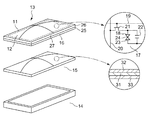
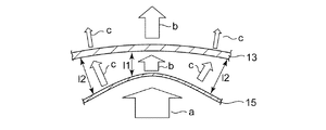
この液晶表示装置は、図1に示すように、周辺に額縁領域11が形成され、この額縁領域11によって囲まれた表示領域12を有し、表示領域12が正面外側方向(視認方向側)に突状に湾曲している液晶表示パネル13を有し、液晶表示パネル13の背面(反視認側)側には平面光源装置(バックライト)14が配置されている。そして、これら液晶表示パネル13と平面光源装置14との間には、偏光反射部材15が介在されている。
As shown in FIG. 1, this liquid crystal display device has a
なお、図中で液晶表示パネル13と偏光反射部材15に描かれている湾曲した実線は、夫々液晶表示パネル13と偏光反射部材15とが長軸及び短軸の両方の実線方向に湾曲していることを示しているものであり、長軸あるいは短軸のいずれか一方の方向にのみ湾曲した構成とすることも可能である。
In the drawing, the curved solid lines drawn on the liquid
この液晶表示パネル13は、ガラス材や合成樹脂材などの可撓性材料から構成される透明絶縁基板16の主面上に、酸化インジウムスズ(ITO)などからなる表示画素17を構成する透明画素電極18がマトリクス状に配置されている。また、これら画素電極18の行方向には複数の走査線19が、画素電極18の列方向には複数本の信号線20が配設されている。
The liquid
この画素電極18に対応して走査線19及び信号線20の交差位置近傍には、スイッチング素子として複数のTFT21を有している。このTFT21は、画素電極18の行に沿って形成される走査線19とゲート電極が接続され、また画素電極18の列に沿って形成される信号線20にソース電極もしくはドレイン電極が接続されており、走査線駆動回路(図示せず)から走査線19を介して供給される駆動電圧によってTFT21が導通し、信号線駆動回路(図示せず)からの信号線20を通して供給される信号電圧をTFT21のソース・ドレイン通路を通して画素電極18に印加するように動作する。
Corresponding to the
さらに、この画素電極18には、保持容量22の一方端が並列に接続されており、この保持容量22の他方端は共通電極23と接続、あるいは補助容量線または前後段の走査線に接続されており、画素電極18と共通電極23との間に液晶層24が配置されている。これらTFT21や画素電極18、走査線19や信号線20などの駆動線の上面には、さらにポリイミドなどから構成される配向膜(図示せず)が設けられてアレイ基板25が構成されている。
Further, one end of the
また、このアレイ基板25と対向する対向基板26は、同様にガラス材や合成樹脂材などの可撓性材料から構成される透明絶縁基板27と、この透明絶縁基板27のアレイ基板25と対向する主面上には、その周辺部分に黒色の遮光膜(図示せず)が設けられるとともに、ITOなどから構成される透明共通電極23が設けられ、この共通電極23の上面には、さらにポリイミドなどからなる配向膜(図示せず)が設けられている。
Further, the
この遮光膜に囲まれた絶縁基板27部分には,アクリル材などから構成される三原色カラーフィルタ(図示せず)、並びに配線間の隙間からの漏光を遮断するためのブラックマトリクス(図示せず)が設けられて対向基板26を構成している。なお、カラーフィルタはアレイ基板25側に形成することも可能である。
The
このアレイ基板25と対向基板26は,所定の間隙を持って対向配置されるとともにシール材(図示せず)を介して貼り合わされており、この間隙部には液晶部材が封止されて液晶層24を形成している。この液晶層24の厚さは、アレイ基板25と対向基板26間に介在されるスペーサ(図示せず)によって規定されて、湾曲された表示領域12を有する液晶表示パネル13が構成されている。
The
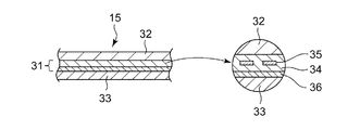
一方、アレイ基板25側の裏面には、偏光層(DBEF:Dual Brightness Enhanced Film)31を拡散フィルム層32、33によって挟み込んだシート状の偏光反射部材15が配置されている。この偏光層31は薄く形成されるために、偏光層31の両面側から拡散フィルム層32,33によってサンドイッチ状に挟むことで偏光層31を補強するとともに、傷付きを抑制することが可能となる。
On the other hand, a sheet-like polarizing
また、拡散フィルム層32,33を使用することによって、拡散によって視角の差を低減し視野角を広くすることが可能となるばかりでなく、ギラギラ感が出てしまう表示を抑制することも可能で、さらに輝度ムラの改善も図ることが可能となる。
この偏光反射部材15の液晶表示パネル13とは反対側となる裏面側には、平面状の平面光源装置14が配置されている。
In addition, by using the
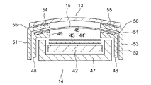
A flat planar
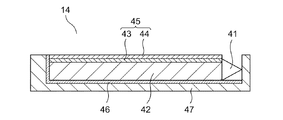
この平面光源装置14は、図2及び図6に示すように、LED及びリフレクタなどからなる光源41からの光を導入して面状の光として出射する平板状に構成された導光板42と、この導光板42の出射面側に順次配置された拡散シート43、レンズシート44などの光学シート45を備えている。光学シート45として、拡散シート43及びレンズシート44の2枚のシートで構成しているが、その順番を入れ替えたり、いずれかのシートを省略することも可能であり、また、更に偏光シートなどの別のシートを追加することも可能であって、その種類や構成には特に限定はされない。平面光源装置14としては、このような導光板42を使用した形態以外にも、LEDを平面状に多数並列に配置した構成や、EL素子からなる平面光源装置14として形成することも可能であり、平面光源装置14としての構成には制限を受けない。
As shown in FIGS. 2 and 6, the planar
一方、導光板42の非出射面側には反射シート46(図6参照)が配置されており、これら反射シート46、導光板42及び光学シート45、光源41などは一括して箱状のバックケース47内に収納され、これら発光構成部材をバックケース47内に固定保持するためのフロントケース48がバックケース47の開放面側から嵌合されており、フロントケース48の中央部分は開口49として発光された光を偏光反射部材15を通して液晶表示パネル13側に通過させるように構成されている。
On the other hand, a reflection sheet 46 (see FIG. 6) is disposed on the non-light-emitting surface side of the
この反射シート46を、図6に示すように、導光板42の底面部分のみならず、光源41を除く導光板42の各側面にまで配置することにより、光の利用効率を更に向上させることが可能となる。
As shown in FIG. 6, the light use efficiency can be further improved by arranging the
このフロントケース48の液晶表示パネル13面側、即ち開口49縁部の外表面は、湾曲状に形成されている液晶表示パネル13の曲面形状に沿うように湾曲形成されている。このフロントケース48は、内側ではバックケース47を保持することから、開口49縁部は、その内側面側がフロントケース48側面と略直角となるように形成し、開口49縁部の外側面側が湾曲するように合成樹脂などの材料で一体に形成することで容易に形成することが可能である。
The liquid
しかしながら、この一体成形にて形成する代わりに、フロントケース48の開口49縁部の肉厚が一定となるように形成しておいて、この開口49縁部の外側に別体として形成される湾曲面を有する枠体(図示せず)を被せる、あるいは接着などの方法にて一体化させて曲面を有する開口49縁部として構成することも可能である。
However, instead of forming by this integral molding, the thickness of the edge portion of the
この開口49縁部の外面、即ち液晶表示パネル13側の面上には、偏光反射部材15が両面接着テープ50などにて取着されている。この偏光反射部材15全体は曲面を有する液晶表示パネル13の曲面に沿うような曲面をもって形成されている。従って、シート状に成形加工されていることが使用上で利便性があるものと考えられる。
On the outer surface of the edge of the
この偏光反射部材15は、図1にて液晶表示装置の概要を説明した際にも説明を行っているが、より詳細には図3に示すように構成されている。
The
即ち、樹脂層34に反射粒子35を混入した材料をPETフィルムなどの基材36に塗布して形成した偏光層(DBEF)(31)を中心に、その両面側を拡散フィルム層32,33にて挟み込んだ構成として形成されている。この反射粒子35は偏光軸と同じ方向(平行)の光、例えばP偏光を通過させ、その偏光軸と異なる方向の光、例えばS偏光に対しては反射させるような材料から形成されている。ここで反射された光は、光学シート45、導光板42方向に戻されて各部材の反射、あるいは反射シート46によって反射され、再度偏光反射部材15に到達して透過、または反射の動作を繰り返すことにより光効率の改善が図られる。
That is, the polarizing layer (DBEF) (31) formed by applying a material in which the
ここでの説明では、基材36を使用することで偏光層31を形成するように説明しているが、基材36を省略して拡散フィルム層32または33のフィルム面に直接塗布して形成するように構成することも可能である。
In the description here, the
このように偏光反射部材15を構成することによって、傷に弱い偏光層31は拡散フィルム層32,33によって保護されると同時に機械的にも補強することが可能となり、また広視野角化も可能でしかも輝度ムラの改善も図ることが可能である。また、視角の差を低減しギラツキ感を抑制した表示を可能とし得るものである。
By constructing the
この偏光反射部材15は、同様な曲面を備えた保持ケース51によってフロントケース48の開口49縁部外面上に位置固定される。この保持ケース51はフロントケース48の側板52に沿う側板53と、この側板53の一端液晶表示パネル13側の端部に形成した縁部54から構成されている。この縁部54は内外面が液晶表示パネル13の曲面とほぼ同じ曲面形状になるように形成されている。
The
即ち、フロントケース48の開口49縁部と保持ケース51の縁部54との間に偏光反射部材15を保持し、保持ケース51の縁部54外面上に液晶表示パネル13を両面接着テープ55などによって固定配置している。この結果、液晶表示パネル13の湾曲曲面と偏光反射部材15の湾曲曲面とは、ほぼ液晶表示パネル13の表示領域12部分と偏光反射部材15の光透過部分との間隔を一定にすることを可能としている。
なお、バックケース47とフロントケース48とは、一方に形成した鉤状部(図示せず)と、他方に形成した開口部(図示せず)との嵌合構造によって両者を一体化させる構成とすることができ、フロントケース48と保持ケース51とを同様に嵌合させる構成を採ることも可能である。
That is, the
The
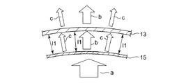
このような構成を採用することによって、図4に示すように、平面光源装置14から出射された光aは偏光反射部材15に入射されるが、拡散フィルム層32,33を備えているので、正面から入射した光aは偏光反射部材15の曲面に応じて夫々鉛直方向に光を出射させていくので、正面から入射した光aを湾曲形成された液晶表示パネル13方向に矢印b,cのように均等に放出させることが可能となる。
By adopting such a configuration, as shown in FIG. 4, the light a emitted from the planar
しかしながら、図5に示すように、液晶表示パネル13と偏光反射部材15との間隔l1が均等でないl2のような場合には、偏光反射部材15から出射された鉛直の光aは液晶表示パネル13に垂直に入射されずに光を減少させる結果となり、この現象が液晶表示パネル13全体として捉えた場合には、光の密の部分と粗の部分とが混在する結果となり、輝度ムラや輝度の低下を助長する原因となっている。
そこで、湾曲している液晶表示パネル13と偏光反射部材15との間隔を、l1=l2、もしくはl1≒l2として実質的に等しい間隔とすることで、換言すれば、液晶表示パネル13と偏光反射部材15との対向している面の曲率を等しく、あるいはほぼ等しくなるように実質的に等しく設定させることで、輝度ムラや輝度の低下を抑制することが可能となる。
However, as shown in FIG. 5, when the distance l1 between the liquid
Therefore, the interval between the curved liquid
この偏光反射部材15を液晶表示パネル13と同じ曲面形状とするために、偏光層(DBEF)31を拡散フィルム層32,33にて挟持させる構成を採っているので、光を均等に伝達させる効果の他にも湾曲形状を形成させる上で極めて有利な構成となっている。この結果として、光源装置として湾曲形成された液晶表示パネル13に対して平面状の平面光源装置14を適用させることが可能となり、光源装置を液晶表示パネル13と同様に湾曲させて構成することがないので、光源装置として簡略化させることが可能となり、従来の平面光源装置のフロントケース48部分を小修整するだけで、基本的な構成をそのまま流用することも可能となるなどの効果を発揮させることが可能となる。
Since the polarizing layer (DBEF) 31 is sandwiched between the diffusing film layers 32 and 33 in order to make the polarized
また、この偏光反射部材15をフロントケース48と保持ケース51とで保持させている形態を採用した場合について説明してきたが、偏光反射部材15を直接液晶表示パネル13に両面接着テープ(図示せず)などによって固定化するように構成することも可能であり、この構成の場合には、液晶表示パネル13と偏光反射部材15との間隔を殆ど無視することができるので、より光の損失を軽減することが可能となる。
Further, the case where the
さらに、この構成を採る場合には、保持ケース51もしくはフロントケース48の何れか一方を省略し、他方の機能を兼用させる構成とすることによって、より簡略化された構成とすることが可能となる。
また、アレイ基板25や対向基板26の構成は、上記説明の構成以外のものでも適用が可能であり、その他、本発明の趣旨を逸脱しない範囲での追加や変更は適宜成し得るものである。
Furthermore, when adopting this configuration, either the holding
The configurations of the
12…表示領域
13…液晶表示パネル
14…平面光源装置
15…偏光反射部材
31…偏光層
32,33…拡散フィルム層
34…樹脂層
35…反射粒子
46…反射シート
DESCRIPTION OF
Claims (4)
この液晶表示パネルの裏面から光を出射する平面光源装置と、
を備える液晶表示装置において、
前記液晶表示パネルの表示面を前記平面光源装置に対して離間する方向に曲面状に配置されるとともに、
前記液晶表示パネルと前記平面光源装置との間に偏光反射部材が配置されていることを特徴とする液晶表示装置。 A liquid crystal display panel in which at least the display area is formed in a curved surface;
A planar light source device for emitting light from the back surface of the liquid crystal display panel;
In a liquid crystal display device comprising:
The display surface of the liquid crystal display panel is arranged in a curved shape in a direction away from the planar light source device, and
A liquid crystal display device, wherein a polarization reflection member is disposed between the liquid crystal display panel and the flat light source device.
Priority Applications (2)
| Application Number | Priority Date | Filing Date | Title |
|---|---|---|---|
| JP2013258959A JP2015114643A (en) | 2013-12-16 | 2013-12-16 | Liquid crystal display device |
| US14/570,168 US20150168784A1 (en) | 2013-12-16 | 2014-12-15 | Liquid crystal display device |
Applications Claiming Priority (1)
| Application Number | Priority Date | Filing Date | Title |
|---|---|---|---|
| JP2013258959A JP2015114643A (en) | 2013-12-16 | 2013-12-16 | Liquid crystal display device |
Publications (1)
| Publication Number | Publication Date |
|---|---|
| JP2015114643A true JP2015114643A (en) | 2015-06-22 |
Family
ID=53368249
Family Applications (1)
| Application Number | Title | Priority Date | Filing Date |
|---|---|---|---|
| JP2013258959A Pending JP2015114643A (en) | 2013-12-16 | 2013-12-16 | Liquid crystal display device |
Country Status (2)
| Country | Link |
|---|---|
| US (1) | US20150168784A1 (en) |
| JP (1) | JP2015114643A (en) |
Cited By (3)
| Publication number | Priority date | Publication date | Assignee | Title |
|---|---|---|---|---|
| WO2017107302A1 (en) * | 2015-12-23 | 2017-06-29 | 深圳市华星光电技术有限公司 | Curved-surface television and fixed base thereof |
| JP2017142918A (en) * | 2016-02-08 | 2017-08-17 | ミネベアミツミ株式会社 | Surface lighting device |
| JP2018137156A (en) * | 2017-02-22 | 2018-08-30 | ミネベアミツミ株式会社 | Planar lighting device |
Families Citing this family (3)
| Publication number | Priority date | Publication date | Assignee | Title |
|---|---|---|---|---|
| CN112034652A (en) * | 2016-04-29 | 2020-12-04 | 群创光电股份有限公司 | Display device |
| CN114415405B (en) | 2021-12-21 | 2024-01-30 | 武汉华星光电技术有限公司 | Display device and manufacturing method thereof |
| TWI820976B (en) * | 2022-10-20 | 2023-11-01 | 達擎股份有限公司 | Display device |
Family Cites Families (3)
| Publication number | Priority date | Publication date | Assignee | Title |
|---|---|---|---|---|
| KR100500715B1 (en) * | 1998-06-26 | 2005-07-12 | 미츠비시덴키 가부시키가이샤 | Liquid crystal display device and manufacturing method thereof |
| US7572490B2 (en) * | 2004-04-27 | 2009-08-11 | Samsung Electronics Co., Ltd. | Brightness enhancement film for liquid crystal display and manufacturing method thereof |
| JP5094250B2 (en) * | 2007-07-10 | 2012-12-12 | 株式会社ジャパンディスプレイイースト | Display device |
-
2013
- 2013-12-16 JP JP2013258959A patent/JP2015114643A/en active Pending
-
2014
- 2014-12-15 US US14/570,168 patent/US20150168784A1/en not_active Abandoned
Cited By (3)
| Publication number | Priority date | Publication date | Assignee | Title |
|---|---|---|---|---|
| WO2017107302A1 (en) * | 2015-12-23 | 2017-06-29 | 深圳市华星光电技术有限公司 | Curved-surface television and fixed base thereof |
| JP2017142918A (en) * | 2016-02-08 | 2017-08-17 | ミネベアミツミ株式会社 | Surface lighting device |
| JP2018137156A (en) * | 2017-02-22 | 2018-08-30 | ミネベアミツミ株式会社 | Planar lighting device |
Also Published As
| Publication number | Publication date |
|---|---|
| US20150168784A1 (en) | 2015-06-18 |
Similar Documents
| Publication | Publication Date | Title |
|---|---|---|
| US10976582B2 (en) | Display | |
| CN107357063B (en) | Display device and splicing display device including the display device | |
| US10180534B2 (en) | Borderless display device including display module | |
| JP5933509B2 (en) | Liquid crystal display | |
| JP5775128B2 (en) | Liquid crystal display | |
| KR102395088B1 (en) | Backlight unit and liquid crystal dispaly device including the same | |
| US20170127166A1 (en) | Lighting device and display device | |
| US20140043848A1 (en) | Backlight device and display device including the same | |
| CN103901642A (en) | Liquid crystal display device | |
| JP2015114643A (en) | Liquid crystal display device | |
| JP2016009686A (en) | Display device | |
| US20170192292A1 (en) | Display | |
| JP5604342B2 (en) | Frame covering member | |
| KR102511041B1 (en) | Backlight unit and liquid crystal display module having the same | |
| JP2012150366A (en) | Light guide member and multi-display device including the same | |
| KR20120057388A (en) | Backlight unit and liquid crystal display device and method having the same | |
| JP5538267B2 (en) | System frame | |
| KR102167144B1 (en) | Liquid crystal display | |
| JP2014142379A (en) | Planar display device | |
| KR102192474B1 (en) | Liquid crystal display device | |
| KR102082679B1 (en) | Liquid crystal display device and method for fabricating the same | |
| KR102230717B1 (en) | Guide Panel And Backlight Unit Including Thereof | |
| WO2012141084A1 (en) | Illumination device, display device, and television receiving device | |
| JP5806908B2 (en) | Image display device | |
| KR102554719B1 (en) | Light emitting diode assembly and backlight unit having the same and liquid crystal display device having the same |