JP5091602B2 - Surface light source device and liquid crystal display device using the same - Google Patents
Surface light source device and liquid crystal display device using the same Download PDFInfo
- Publication number
- JP5091602B2 JP5091602B2 JP2007247391A JP2007247391A JP5091602B2 JP 5091602 B2 JP5091602 B2 JP 5091602B2 JP 2007247391 A JP2007247391 A JP 2007247391A JP 2007247391 A JP2007247391 A JP 2007247391A JP 5091602 B2 JP5091602 B2 JP 5091602B2
- Authority
- JP
- Japan
- Prior art keywords
- light
- guide plate
- liquid crystal
- light guide
- adhesive tape
- Prior art date
- Legal status (The legal status is an assumption and is not a legal conclusion. Google has not performed a legal analysis and makes no representation as to the accuracy of the status listed.)
- Active
Links
Images


Description
本発明は、光源からの光を導光板を通して面状に照射する面光源装置に関するものであり、さらには、係る面光源装置が組み込まれた液晶表示装置に関する。 The present invention relates to a surface light source device that irradiates light from a light source in a planar manner through a light guide plate, and further relates to a liquid crystal display device incorporating such a surface light source device.
近年、パーソナルコンピュータやワードプロセッサ等の情報機器の表示装置、テレビ、ビデオムービー、カーナビゲーションシステム等の映像機器の表示装置として、軽量、薄型、低消費電力という特長を持つ液晶表示装置が多用されている。このような液晶表示装置においては、明るい表示画面を実現するために、液晶パネルの背後から照明光を当てるためのバックライトユニット(面光源装置)を内蔵した構成を採るものが多い。 In recent years, liquid crystal display devices having features such as light weight, thinness, and low power consumption are widely used as display devices for information devices such as personal computers and word processors, and display devices for video devices such as televisions, video movies, and car navigation systems. . In many cases, such a liquid crystal display device adopts a configuration in which a backlight unit (surface light source device) for applying illumination light from behind the liquid crystal panel is incorporated in order to realize a bright display screen.
ここで、バックライトユニットは、光源の配置箇所によってエッジライト方式と直下方式とに分類される。例えばエッジライト方式は、液晶パネルに対向する導光板のエッジにLED等の点光源装置を配置する方式である。また、直下方式は、蛍光放電管等の直管状の光源を液晶パネルの裏面に複数配置し、液晶パネルと光源との間に拡散板を配置する方式である。これら方式のうち、エッジライト方式は、薄型化の点で有利であり、例えば携帯用電子機器やノート型のパーソナルコンピュータの表示装置に適した方式と言うことができる。 Here, the backlight unit is classified into an edge light system and a direct system according to the location of the light source. For example, the edge light system is a system in which a point light source device such as an LED is disposed on the edge of a light guide plate facing a liquid crystal panel. The direct method is a method in which a plurality of straight tubular light sources such as fluorescent discharge tubes are arranged on the back surface of the liquid crystal panel, and a diffusion plate is arranged between the liquid crystal panel and the light source. Among these methods, the edge light method is advantageous in terms of thinning, and can be said to be a method suitable for a display device of a portable electronic device or a notebook personal computer, for example.
ところで、例えば前記エッジライト方式のバックライトユニットの場合、通常、光源からの光を導光板によって面状光に変換し、所定の方向に照射されるようにする。したがって、液晶パネルを前記導光板上に重ねて配置する必要があり、面光源装置と液晶パネルの外周部を遮光粘着テープを用いて固定することが行われている(例えば、特許文献1等を参照)。 Incidentally, for example, in the case of the edge light type backlight unit, light from a light source is usually converted into planar light by a light guide plate so as to be irradiated in a predetermined direction. Therefore, it is necessary to arrange the liquid crystal panel so as to overlap the light guide plate, and the outer periphery of the surface light source device and the liquid crystal panel is fixed using a light-shielding adhesive tape (for example, Patent Document 1). reference).
特許文献1記載の発明は、主に光反射性と遮光性を備えた両面粘着テープに関するものであるが、前記両面粘着テープを用いて、フレキシブルプリント回路基板に挟持された液晶表示パネルとバックライト筐体とを固着した液晶表示モジュールユニットが開示されている。
ところで、通常、液晶パネルにはその両面に偏光フィルムが貼り付けられており、これが段差になるため、組み合わされる面光源装置においては、前記段差に対応して導光板の端部を傾斜面とする等の工夫が施されている。前記傾斜面を形成することで、偏光フィルムと液晶パネルのガラス基板との間の段差を吸収することができ、有効発光領域上に偏光フィルムを収容する空間を形成することができる。 By the way, since a polarizing film is usually attached to both surfaces of a liquid crystal panel and this forms a step, in the combined surface light source device, the end portion of the light guide plate is inclined according to the step. Etc. are applied. By forming the inclined surface, a step between the polarizing film and the glass substrate of the liquid crystal panel can be absorbed, and a space for accommodating the polarizing film can be formed on the effective light emitting region.
ただし、この場合、前記傾斜面とされた部分からの光漏れが問題となるため、導光板の傾斜面部分にも遮光粘着テープを貼り付け、光漏れを防ぐような構造が採用されている。導光板の端部(入光部)から有効発光領域までの間の領域を遮光粘着テープで覆ってしまえば、この部分から光が漏れることはなく、外観上の問題が生ずることはない。 However, in this case, since light leakage from the inclined surface becomes a problem, a structure is adopted in which a light shielding adhesive tape is attached to the inclined surface portion of the light guide plate to prevent light leakage. If the region between the end portion (light incident portion) of the light guide plate and the effective light emitting region is covered with a light-blocking adhesive tape, light does not leak from this portion, and no problem in appearance occurs.
しかしながら、遮光のために前記導光板に直接遮光粘着テープを貼り付けると、粘着剤が導光板と対向することとなり、輝度が低下する原因となっている。例えばモバイル向け液晶モジュール用バックライト等においては、さらなる高輝度化が求められており、前記輝度の低下は大きな問題である。 However, if a light-shielding adhesive tape is directly attached to the light guide plate for light shielding, the adhesive will face the light guide plate, causing a decrease in luminance. For example, backlights for liquid crystal modules for mobile use and the like are required to have higher luminance, and the reduction in luminance is a serious problem.
本発明は、このような従来の実情に鑑みて提案されたものであり、導光板への粘着テープの貼り付けによる輝度低下を解消することが可能な面光源装置を提供することを目的とし、さらには液晶表示装置を提供することを目的とする。 The present invention has been proposed in view of such a conventional situation, and an object of the present invention is to provide a surface light source device capable of eliminating a decrease in luminance due to adhesion of an adhesive tape to a light guide plate. Furthermore, it aims at providing a liquid crystal display device.
前述の目的を達成するために、本発明に係る面光源装置は、光源と、光源からの光を所定の方向に導く導光板と、導光板上に重ねられた光学フィルム群と、それらが組み込まれたフレームと、その粘着剤によってフレームに貼り付けられた枠状の遮光粘着テープとを備え、前記導光板は、前記光源の光が入光される入光部から液晶パネルに対する有効発光領域までの間の領域が液晶パネルの段差に対応した傾斜面とされており、前記遮光粘着テープの前記導光板の傾斜面に対向する箇所には遮光機能を有する短冊状のテープ片が配されているとともに前記短冊状のテープ片の前記導光板の傾斜面に対向する面には粘着剤が塗布されていない構成となっており、かつ、前記短冊状のテープ片の両端部分が前記遮光粘着テープの粘着部に貼り付けられていることを特徴とする。 In order to achieve the above-described object, a surface light source device according to the present invention includes a light source, a light guide plate that guides light from the light source in a predetermined direction, a group of optical films stacked on the light guide plate, and a combination thereof. And a frame-shaped light-shielding adhesive tape attached to the frame with the adhesive, and the light guide plate extends from a light incident portion where light from the light source is incident to an effective light emission region for the liquid crystal panel. The area between the two is an inclined surface corresponding to the level difference of the liquid crystal panel, and a strip-shaped tape piece having a light shielding function is arranged at a location facing the inclined surface of the light guide plate of the light shielding adhesive tape. And the adhesive is not applied to the surface of the strip-shaped tape piece facing the inclined surface of the light guide plate, and both end portions of the strip-shaped tape piece are made of the light-shielding adhesive tape. Paste to adhesive part It is characterized in that is.
また、本発明の液晶表示装置は、光源と、光源からの光を所定の方向に導く導光板と、導光板上に重ねられた光学フィルム群と、それらが組み込まれたフレームと、その粘着剤によってフレームに貼り付けられた枠状の遮光粘着テープと、フレームによって支持されて遮光粘着テープによって固定された液晶パネルとを備え、前記導光板は、前記光源の光が入光される入光部から液晶パネルに対する有効発光領域までの間の領域が液晶パネルの段差に対応した傾斜面とされており、前記遮光粘着テープの前記導光板の傾斜面に対向する箇所には遮光機能を有する短冊状のテープ片が配されているとともに前記短冊状のテープ片の前記導光板の傾斜面に対向する面には粘着剤が塗布されていない構成となっており、かつ、前記短冊状のテープ片の両端部分が前記遮光粘着テープの粘着部に貼り付けられていることを特徴とする。 Further, the liquid crystal display device of the present invention includes a light source, a light guide plate that guides light from the light source in a predetermined direction, an optical film group superimposed on the light guide plate, a frame in which they are incorporated, and an adhesive thereof And a liquid crystal panel supported by the frame and fixed by the light shielding adhesive tape, and the light guide plate is a light incident portion into which light from the light source is incident The area from the effective light emitting area to the liquid crystal panel is an inclined surface corresponding to the step of the liquid crystal panel, and a strip shape having a light shielding function is provided at a location facing the inclined surface of the light guide plate of the light shielding adhesive tape of the surface facing the inclined surface of the light guide plate of the strip-shaped tape strip with tape pieces are disposed has a structure in which the adhesive is not applied, and the strip-shaped tape piece Wherein the end portions is attached to the adhesive portion of the light shielding adhesive tape.
本発明によれば、光源の入光部から前記液晶パネルに対する有効発光領域までの間の領域において、輝度低下が避けられる。 According to the present invention, it is possible to avoid a decrease in luminance in a region between a light incident part of a light source and an effective light emitting region for the liquid crystal panel .
前記導光板においては、光源の入光部から前記液晶パネルに対する有効発光領域までの間の領域の遮光を図る必要がある。 In the light guide plate, it is necessary to shield the light from the light incident portion of the light source to the effective light emitting region for the liquid crystal panel .
例えば、前記導光板の光源の入光部から前記液晶パネルに対する有効発光領域までの間の領域に、粘着剤が塗布されていない遮光テープ、あるいは液晶パネルと対向する面にのみ粘着剤層が形成された遮光片面粘着テープを配することで、本発明が実現される。 For example, the region between the light incident portion of the light source of the light guide plate to the effective light emitting region with respect to the liquid crystal panel, the light shielding tape adhesive is not applied, or a liquid crystal panel facing the only surface adhesive layer formed The present invention is realized by arranging the light-shielding single-sided adhesive tape.
本発明によれば、導光板への粘着テープの貼り付けによる輝度低下のない面光源装置を提供することができ、さらには表示品位に優れた液晶表示装置を提供することが可能である。 ADVANTAGE OF THE INVENTION According to this invention, the surface light source device without a brightness fall by sticking of the adhesive tape to a light-guide plate can be provided, Furthermore, it is possible to provide the liquid crystal display device excellent in the display quality.
以下、本発明に係る面光源装置及びこれを用いた液晶表示装置について説明する。 Hereinafter, a surface light source device according to the present invention and a liquid crystal display device using the same will be described.
(第1の実施形態)
本実施形態の面光源装置は、光学フィルム群を構成する光学フィルムの一部を光源の入光部まで拡大し、遮光粘着テープと導光板の間に介在させることで遮光粘着テープの粘着面が導光板と直接接触しないように構成した例である。
(First embodiment)
In the surface light source device of this embodiment, a part of the optical film constituting the optical film group is expanded to the light incident part of the light source, and interposed between the light shielding adhesive tape and the light guide plate, whereby the adhesive surface of the light shielding adhesive tape is guided. It is the example comprised so that it might not contact with an optical plate directly.
先ず、図1に面光源装置(バックライトユニット)1の基本構成を示す。バックライトユニット1は、図1に示すように、点光源装置であるLEDチップ2が実装されたフレキシブル基板3、導光板4、反射シート5及び光学フィルム群6から構成されており、点光源であるLEDチップ2の光が前記導光板4によって面状光に変換される。
First, FIG. 1 shows a basic configuration of a surface light source device (backlight unit) 1. As shown in FIG. 1, the backlight unit 1 includes a flexible substrate 3 on which an
前記LEDチップ2は、例えば発光ダイオード素子(LED)が封止樹脂内に埋め込まれて構成され、その側面からフレキシブル基板3の実装面と平行に光を照射する、いわゆるサイドビュー方式のLEDチップである。本例の場合、LEDチップ2はフレキシブル基板3の長手方向に沿って複数配列されており、また各LEDチップ2はほぼ等間隔に配列されている。
The
前記LEDチップ2は、その一側面(導光板4側の側面)から光が発せられる。すなわち、前記側面が出光面である。そして、導光板4の端面とLEDチップ2の出光面とが接することで、LEDチップ2から発せされた光が導光板4へと導かれ、面状の光に変換される。
The
導光板4においては、前記LEDチップ2と対向する端面4aが入光部であり、後述の液晶パネルに設けられる偏光フィルムの段差を吸収するために、前記入光部(端面4a)から有効発光領域までの間の領域が傾斜面4bとされている。
In the
また、前記導光板4の裏面側には反射シート5が貼り付けられており、LEDチップ2の光が導光板4の裏面側から漏洩するのを防止し、光の損失を最小限に抑えるように構成されている。
In addition, a
一方、前記導光板4の表面側(光照射面側)には、照射される光の均一性の向上や輝度向上等を目的に、複数の光学フィルムからなる光学フィルム群6が設置されている。光学フィルム群6を構成する光学フィルムは、本例の場合、光を均一化するための拡散シート61、及び2枚のプリズムフィルム(レンズフィルム)62、63である。
On the other hand, on the surface side (light irradiation surface side) of the
これら光学フィルムのうち、拡散シート61は、導光板4を透過して照射される光を拡散して均一化する役割を果たすものであり、例えば光透過性の樹脂フィルム中に光拡散粒子を分散したフィルム等が使用される。樹脂フィルムとしては、例えばポリエチレンテレフタレートやポリカーボネート等のフィルムが用いられる。前記プリズムフィルム62,63は、光を一方向に集光して輝度を向上する役割を果たすものであり、集光機能を有するプリズムが配列された形態を有するフィルムである。導光板4や拡散フィルム61を透過した光は、このプリズムフィルム62,63によって所定の方向(フィルム面に対してほぼ直交する方向)に揃えられ、効率的な光照射が行われ、結果として輝度向上が図られる。
Among these optical films, the
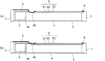
前述の各構成要素は、樹脂フレーム7に組み込まれ、その外周部に、例えば上面が黒色、下面が白色とされた枠状の遮光粘着テープ8が貼り付けられる。遮光粘着テープ8は、図2に示すように、導光板4の外周部分を覆う形で貼り付けられるが、導光板4の前記入光部(端面4a)から前記液晶パネルに対する有効発光領域までの間の領域に対応して面積が拡大されており、傾斜面4b上にも貼り付けられる。これは、導光板4の前記入光部(端面4a)から前記液晶パネルに対する有効発光領域までの間の領域における光漏れを防止するためである。
Each of the above-described components is incorporated in the
ただし、図3(a)に示すように、導光板4の傾斜面4b上に直接遮光粘着テープ8を貼り付けると、輝度低下に繋がるという問題がある。
However, as shown in FIG. 3 (a), when the paste directly shielding
本実施形態では、光学フィルム群6のうちの拡散シート61の面積を前記傾斜面4上を覆うように拡大し、導光板4と遮光粘着テープ8の間に介在させるようにしている。
In the present embodiment, the area of the
導光板4と遮光粘着テープ8の間に介在させる光学フィルムとしては、前記拡散シート61に限らず、任意の光学フィルムを選択することができる。ただし、前記プリズムフィルム62,63を拡大して介在させた場合、プリズムの働きにより入射光が散乱され、不用意に光漏れが発生する可能性もあるので、前記拡散シート61を介在させることが好ましい。また、面積を拡大して導光板4と遮光粘着テープ8の間に介在させる光学フィルムは、光学フィルム群6のうちの一部とする必要がある。全ての光学フィルムを拡大すると、液晶パネルに貼り付けられた偏光フィルムを収容する上で支障をきたすおそれがある。
The optical film interposed between the
以上の構成を有する面光源装置は、液晶表示装置において、バックライトユニットとして組み込まれる。そこで次に、前述の面光源装置を組み込んだ液晶表示装置について説明する。 The surface light source device having the above configuration is incorporated as a backlight unit in a liquid crystal display device. Next, a liquid crystal display device incorporating the above-described surface light source device will be described.
図4は、面光源装置(バックライトユニット)が組み込まれた液晶表示装置を分解して示すものである。本実施形態の液晶表示装置は、図4に示すように、液晶パネル11と前述の面光源装置1とを備え、これらの周囲を前述の樹脂フレーム7で保持し一体化するようにしている。
FIG. 4 is an exploded view of a liquid crystal display device in which a surface light source device (backlight unit) is incorporated. As shown in FIG. 4, the liquid crystal display device of this embodiment includes a
液晶パネル11は、例えばアレイ基板と対向基板の間に液晶材料を封入することにより構成され、アレイ基板には表示画素に対応して画素電極及びスイッチング素子(薄膜トランジスタ)がマトリクス状に形成されている。また、アレイ基板には、画素電極に電気信号を送るための信号線と、スイッチング素子である薄膜トランジスタにスイッチング信号を供給するためのゲート線とが互いに直交して配線されている。一方、対向基板には、対向電極が透明電極材料(例えばITO等)によりほぼ全面に形成されており、各画素に対応してカラーフィルタ層が形成されている。さらに、前記アレイ基板と対向基板の外表面には、それぞれ偏光板を偏光軸が互いに直交するように貼り合わされている。
The
液晶パネル11には、駆動信号を供給するLSI12が実装されており、外部回路基板からの駆動信号に基づいて前記スイッチング素子が駆動されることで画像表示が行われる。この画像表示が行われる領域が表示領域であり、前記液晶パネル11は多数の画素が配列された表示領域を有することになる。
An
前記バックライトユニットとして用いられる面光源装置1は、前記液晶パネル11の背面側から光照射し、液晶パネル11の表示を明るく見やすい状態とするものである。そして、その主要な構成要素として、前述の通り、光源であるLEDチップ2からの光を前記液晶パネル11の背面に光照射するための導光板4と、この導光板4の裏面側に配される反射シート5と、導光板4の表面側に配される光学フィルム群6とを備えている。光源であるLEDチップ2は、前記導光板4の少なくとも一辺に沿って設けられており、本実施形態の場合、LEDチップ2が実装されたフレキシブル基板3が導光板4の短辺側に設置されている。
The surface light source device 1 used as the backlight unit emits light from the back side of the
光源であるLEDチップ2から出射された光は、直接又は反射シート5により反射されて導光板4へ導かれ、導光板4及び光学フィルム群6を通過した後、液晶パネル11に照射される。液晶パネル11では照射された光が透過され、文字や映像等の画像が所定の明るさで表示されることになる。
Light emitted from the
液晶パネル11の固定には、枠状の遮光接着シート8が用いられ、当該遮光粘着シート8により液晶パネル11を樹脂フレーム7に接着固定することで、液晶パネル11と面光源装置1とが一体に組み付けられる。図5は、面光源装置1に液晶パネル11を固定する際の配置を示すものである。液晶パネル11の両面には偏光フィルム13,14が貼り付けられているが、導光板4に傾斜面4bを形成することにより形成される空間に、偏光フィルム14の貼り付けによる段差部が収容される形になっている。
For fixing the
本実施形態の液晶表示装置においては、前述の通り、遮光粘着テープ8が導光板4の入光部(端面4a)から前記液晶パネルに対する有効発光領域までの間の領域に対応して面積が拡大されており、傾斜面4b上に拡散シート61を介して貼り付けられている。実際、本発明者が液晶表示装置を組み立てて確認したところ、遮光粘着テープ8を導光板4に直接貼り付けた場合に比べて7%程度の輝度向上が認められた。また、導光板4の傾斜面4b上にも遮光粘着テープ8が配される形になっているので、導光板4の入光部(端面4a)から前記液晶パネルに対する有効発光領域までの間の領域からの光漏れも確実に防止される。
In the liquid crystal display device of the present embodiment, as described above, the area of the light-shielding
(第2の実施形態)
本実施形態は、遮光粘着テープ8の一部を非粘着シートに置き換えた例である。その他の構成は、先の第1の実施形態の面光源装置、液晶表示装置と同様であるので、ここでは、本実施形態で用いられる遮光粘着テープ8の構成についてのみ説明する。
(Second Embodiment)
The present embodiment is an example in which a part of the light shielding
本実施形態の面光源装置及び液晶表示装置において用いられる遮光粘着テープ8は、図6に示すように、枠状の両面粘着テープ部8aと、前記導光板4の傾斜面4bに対応して配される非粘着テープ片8bとから構成されている。非粘着テープ片8bは、両面粘着テープ部8aとは別体に形成された短冊状の部材であり、遮光機能は有するが、そのいずれの面にも粘着剤層は形成されていない。また、非粘着テープ片8bは、その両端部分が前記両面粘着テープ部8aに貼り付けられている。
The light-shielding
図7は、前記遮光粘着テープ8の面光源装置1への貼り付け状態を示すものである。樹脂フレーム7上には、両面粘着テープ部8aが貼り付けられ、この上に液晶パネル11を固定できるようになっている。一方、導光板4の傾斜面4b上には、前記非粘着テープ片8bが載置される形になる。ここで、前記非粘着テープ片8bには粘着剤層が形成されておらず、輝度低下が防止される。また、非粘着テープ片8bが遮光機能を有することから、導光板4の入光部(端面4a)から前記液晶パネルに対する有効発光領域までの間の領域から光漏れが生ずることもない。
FIG. 7 shows a state where the light-shielding
(第3の実施形態)
本実施形態は、遮光粘着テープ8の一部を片面粘着テープとした例である。その他の構成は、先の第1の実施形態の面光源装置、液晶表示装置と同様であるので、ここでは、本実施形態で用いられる遮光粘着テープ8の構成についてのみ説明する。
(Third embodiment)
The present embodiment is an example in which a part of the light shielding
本実施形態の面光源装置及び液晶表示装置において用いられる遮光粘着テープ8は、図8に示すように、枠状の両面粘着テープとして形成されるものであるが、導光板4の傾斜面4b(導光板4の入光部から前記液晶パネルに対する有効発光領域までの間の領域)と対向する部分(図中、斜線部分)8cについては、粘着剤層が形成されていない。
The light-shielding
導光板4の傾斜面4bには片面粘着テープとされた部分8cが接触することになり、輝度低下が防止される。また、片面粘着テープとされた部分8cも遮光機能は有するので、導光板4の入光部(端面4a)から前記液晶パネルに対する有効発光領域までの間の領域から光漏れが生ずることもない。
The
1 面光源装置、2 LEDチップ、3 フレキシブル基板、4 導光板、5 反射シート、6 光学フィルム群、7 樹脂フレーム、8 遮光粘着テープ、8a 両面粘着テープ部、8b 非粘着テープ片、11 液晶パネル、12 LSI、13,14 偏光フィルム、61 拡散シート、62,63 プリズムフィルム DESCRIPTION OF SYMBOLS 1 Surface light source device, 2 LED chip, 3 Flexible substrate, 4 Light guide plate, 5 Reflective sheet, 6 Optical film group, 7 Resin frame, 8 Light-shielding adhesive tape, 8a Double-sided adhesive tape part, 8b Non-adhesive tape piece, 11 Liquid crystal panel , 12 LSI, 13, 14 Polarizing film, 61 Diffusion sheet, 62, 63 Prism film
Claims (4)
前記遮光粘着テープの前記導光板の傾斜面に対向する箇所には遮光機能を有する短冊状のテープ片が配されているとともに前記短冊状のテープ片の前記導光板の傾斜面に対向する面には粘着剤が塗布されていない構成となっており、かつ、前記短冊状のテープ片の両端部分が前記遮光粘着テープの粘着部に貼り付けられていることを特徴とする面光源装置。 A light source, a light guide plate for guiding light from the light source in a predetermined direction, an optical film group superimposed on the light guide plate, a frame in which they are incorporated, and a frame-like shape attached to the frame by the adhesive A light-shielding adhesive tape, and the light guide plate has an inclined surface corresponding to a step of the liquid crystal panel in a region between a light incident portion where light from the light source is incident and an effective light emission region for the liquid crystal panel. ,
A strip-shaped tape piece having a light-shielding function is disposed at a location facing the inclined surface of the light guide plate of the light-shielding adhesive tape, and the strip-shaped tape piece is opposed to the inclined surface of the light guide plate. The surface light source device has a configuration in which no adhesive is applied, and both end portions of the strip-shaped tape piece are attached to the adhesive portion of the light-shielding adhesive tape .
前記遮光粘着テープの前記導光板の傾斜面に対向する箇所には遮光機能を有する短冊状のテープ片が配されているとともに前記短冊状のテープ片の前記導光板の傾斜面に対向する面には粘着剤が塗布されていない構成となっており、かつ、前記短冊状のテープ片の両端部分が前記遮光粘着テープの粘着部に貼り付けられていることを特徴とする液晶表示装置。 A light source, a light guide plate for guiding light from the light source in a predetermined direction, an optical film group superimposed on the light guide plate, a frame in which they are incorporated, and a frame-like shape attached to the frame by the adhesive A light-shielding adhesive tape; and a liquid crystal panel supported by a frame and fixed by the light-shielding adhesive tape, wherein the light guide plate extends from a light incident portion where light of the light source is incident to an effective light emission region for the liquid crystal panel. Is an inclined surface corresponding to the step of the liquid crystal panel,
A strip-shaped tape piece having a light-shielding function is disposed at a location facing the inclined surface of the light guide plate of the light-shielding adhesive tape, and the strip-shaped tape piece is opposed to the inclined surface of the light guide plate. Has a configuration in which no adhesive is applied, and both end portions of the strip-shaped tape piece are attached to the adhesive portion of the light-shielding adhesive tape .
Priority Applications (1)
| Application Number | Priority Date | Filing Date | Title |
|---|---|---|---|
| JP2007247391A JP5091602B2 (en) | 2007-09-25 | 2007-09-25 | Surface light source device and liquid crystal display device using the same |
Applications Claiming Priority (1)
| Application Number | Priority Date | Filing Date | Title |
|---|---|---|---|
| JP2007247391A JP5091602B2 (en) | 2007-09-25 | 2007-09-25 | Surface light source device and liquid crystal display device using the same |
Publications (2)
| Publication Number | Publication Date |
|---|---|
| JP2009080947A JP2009080947A (en) | 2009-04-16 |
| JP5091602B2 true JP5091602B2 (en) | 2012-12-05 |
Family
ID=40655554
Family Applications (1)
| Application Number | Title | Priority Date | Filing Date |
|---|---|---|---|
| JP2007247391A Active JP5091602B2 (en) | 2007-09-25 | 2007-09-25 | Surface light source device and liquid crystal display device using the same |
Country Status (1)
| Country | Link |
|---|---|
| JP (1) | JP5091602B2 (en) |
Cited By (1)
| Publication number | Priority date | Publication date | Assignee | Title |
|---|---|---|---|---|
| CN108227071A (en) * | 2018-01-31 | 2018-06-29 | 广东欧珀移动通信有限公司 | A kind of backlight module and electronic device |
Families Citing this family (14)
| Publication number | Priority date | Publication date | Assignee | Title |
|---|---|---|---|---|
| KR101313653B1 (en) | 2009-06-24 | 2013-10-02 | 엘지디스플레이 주식회사 | Liquid crystal display device |
| JP2012014909A (en) * | 2010-06-30 | 2012-01-19 | Omron Corp | Plane light source device |
| JP5663434B2 (en) | 2011-08-15 | 2015-02-04 | 株式会社ジャパンディスプレイ | Display device |
| JP5917940B2 (en) * | 2012-02-21 | 2016-05-18 | ミネベア株式会社 | Surface lighting device |
| TWI446067B (en) * | 2012-06-29 | 2014-07-21 | Au Optronics Corp | Backlight module |
| JP2014203602A (en) * | 2013-04-02 | 2014-10-27 | ミネベア株式会社 | Planar lighting device |
| WO2015040699A1 (en) | 2013-09-18 | 2015-03-26 | Nltテクノロジー株式会社 | Planar light source device and liquid crystal display device |
| CN103823319B (en) * | 2014-03-10 | 2016-03-09 | 深圳市华星光电技术有限公司 | Backlight module and the liquid crystal indicator with this backlight module |
| CN104456302B (en) * | 2014-11-17 | 2017-03-08 | 深圳市华星光电技术有限公司 | Backlight module and display |
| JP6215867B2 (en) * | 2015-05-22 | 2017-10-18 | ミネベアミツミ株式会社 | Surface lighting device |
| CN108153043B (en) | 2016-12-02 | 2021-01-26 | 美蓓亚三美株式会社 | Planar lighting device |
| JP6608886B2 (en) * | 2016-12-02 | 2019-11-20 | ミネベアミツミ株式会社 | Surface lighting device |
| CN107179577A (en) * | 2017-06-07 | 2017-09-19 | 武汉华星光电技术有限公司 | A kind of backlight module and display device |
| CN112485939A (en) * | 2020-12-04 | 2021-03-12 | 深圳市瀚达美电子有限公司 | Integrated vehicle-mounted display with atmosphere lamp module |
Family Cites Families (5)
| Publication number | Priority date | Publication date | Assignee | Title |
|---|---|---|---|---|
| JP2000310703A (en) * | 1999-04-27 | 2000-11-07 | Matsushita Electric Ind Co Ltd | Back light |
| JP4707260B2 (en) * | 2001-05-14 | 2011-06-22 | 東芝モバイルディスプレイ株式会社 | LIGHTING UNIT, ITS MANUFACTURING METHOD, AND LIQUID CRYSTAL DISPLAY DEVICE USING THE LIGHTING UNIT |
| JP4279761B2 (en) * | 2004-09-27 | 2009-06-17 | 日本ライツ株式会社 | Flat illumination device and liquid crystal display device |
| JP4973905B2 (en) * | 2005-03-18 | 2012-07-11 | Dic株式会社 | Light blocking adhesive tape for LCD module fixing |
| JP4655981B2 (en) * | 2005-05-17 | 2011-03-23 | ソニー株式会社 | Light guide plate and display device including light guide plate |
-
2007
- 2007-09-25 JP JP2007247391A patent/JP5091602B2/en active Active
Cited By (2)
| Publication number | Priority date | Publication date | Assignee | Title |
|---|---|---|---|---|
| CN108227071A (en) * | 2018-01-31 | 2018-06-29 | 广东欧珀移动通信有限公司 | A kind of backlight module and electronic device |
| CN108227071B (en) * | 2018-01-31 | 2020-07-03 | Oppo广东移动通信有限公司 | Backlight module and electronic device |
Also Published As
| Publication number | Publication date |
|---|---|
| JP2009080947A (en) | 2009-04-16 |
Similar Documents
| Publication | Publication Date | Title |
|---|---|---|
| JP5091602B2 (en) | Surface light source device and liquid crystal display device using the same | |
| KR101621535B1 (en) | Backlight unit and liquid crystal display device having the same | |
| KR100610949B1 (en) | Lighting apparatus, electrooptical apparatus and electronic equipment | |
| JP4333727B2 (en) | ELECTRO-OPTICAL DEVICE, LIGHTING DEVICE, AND ELECTRONIC DEVICE | |
| US9322981B2 (en) | Liquid display apparatus | |
| US8212957B2 (en) | Mount structure, illumination apparatus and liquid crystal apparatus | |
| JP5173640B2 (en) | Backlight unit and method for assembling the same | |
| US20150362652A1 (en) | Lighting device, display device, and television receiving device | |
| JP2018142014A (en) | Display device | |
| US20160062034A1 (en) | Display device | |
| JP2009205866A (en) | Illumination unit and liquid crystal display device | |
| JP2009117272A (en) | Liquid display device | |
| JP5529427B2 (en) | Electro-optical device and electronic apparatus | |
| JP2008123915A (en) | Surface light source and liquid crystal display device using this | |
| KR101481836B1 (en) | Backlight unit and liquid crystal display device having the same | |
| JP5013524B2 (en) | Backlight unit and liquid crystal display device | |
| JP2013171619A (en) | Display device, and television receiver | |
| JP2004233810A (en) | Surface light source unit, electrooptical device, and electronic device | |
| KR101737799B1 (en) | Light shielding tape and backlight unit using the same and liquid crystal display device having thereof | |
| JP5271653B2 (en) | Liquid crystal device and electronic device | |
| JP2008123931A (en) | Lighting device, electro-optical device, and electronic apparatus | |
| KR20130071925A (en) | Liquid crystal display module inculding backlight unit | |
| JP2010205614A (en) | Illumination unit, and liquid crystal display device equipped with this illumination unit | |
| JP2010085549A (en) | Liquid crystal device and electronic apparatus | |
| US20150177446A1 (en) | Display device and television device |
Legal Events
| Date | Code | Title | Description |
|---|---|---|---|
| A621 | Written request for application examination |
Free format text: JAPANESE INTERMEDIATE CODE: A621 Effective date: 20100618 |
|
| A977 | Report on retrieval |
Free format text: JAPANESE INTERMEDIATE CODE: A971007 Effective date: 20111111 |
|
| A131 | Notification of reasons for refusal |
Free format text: JAPANESE INTERMEDIATE CODE: A131 Effective date: 20111201 |
|
| A521 | Request for written amendment filed |
Free format text: JAPANESE INTERMEDIATE CODE: A523 Effective date: 20120127 |
|
| A131 | Notification of reasons for refusal |
Free format text: JAPANESE INTERMEDIATE CODE: A131 Effective date: 20120413 |
|
| A521 | Request for written amendment filed |
Free format text: JAPANESE INTERMEDIATE CODE: A523 Effective date: 20120531 |
|
| TRDD | Decision of grant or rejection written | ||
| A01 | Written decision to grant a patent or to grant a registration (utility model) |
Free format text: JAPANESE INTERMEDIATE CODE: A01 Effective date: 20120820 |
|
| A01 | Written decision to grant a patent or to grant a registration (utility model) |
Free format text: JAPANESE INTERMEDIATE CODE: A01 |
|
| A61 | First payment of annual fees (during grant procedure) |
Free format text: JAPANESE INTERMEDIATE CODE: A61 Effective date: 20120914 |
|
| FPAY | Renewal fee payment (event date is renewal date of database) |
Free format text: PAYMENT UNTIL: 20150921 Year of fee payment: 3 |
|
| R150 | Certificate of patent or registration of utility model |
Ref document number: 5091602 Country of ref document: JP Free format text: JAPANESE INTERMEDIATE CODE: R150 |
|
| R250 | Receipt of annual fees |
Free format text: JAPANESE INTERMEDIATE CODE: R250 |
|
| R250 | Receipt of annual fees |
Free format text: JAPANESE INTERMEDIATE CODE: R250 |
|
| R250 | Receipt of annual fees |
Free format text: JAPANESE INTERMEDIATE CODE: R250 |
|
| R250 | Receipt of annual fees |
Free format text: JAPANESE INTERMEDIATE CODE: R250 |
|
| R250 | Receipt of annual fees |
Free format text: JAPANESE INTERMEDIATE CODE: R250 |
|
| R250 | Receipt of annual fees |
Free format text: JAPANESE INTERMEDIATE CODE: R250 |
|
| S111 | Request for change of ownership or part of ownership |
Free format text: JAPANESE INTERMEDIATE CODE: R313111 |
|
| R350 | Written notification of registration of transfer |
Free format text: JAPANESE INTERMEDIATE CODE: R350 |
|
| R250 | Receipt of annual fees |
Free format text: JAPANESE INTERMEDIATE CODE: R250 |
|
| R250 | Receipt of annual fees |
Free format text: JAPANESE INTERMEDIATE CODE: R250 |
|
| R250 | Receipt of annual fees |
Free format text: JAPANESE INTERMEDIATE CODE: R250 |