JP2014112139A - Display device - Google Patents
Display device Download PDFInfo
- Publication number
- JP2014112139A JP2014112139A JP2012266148A JP2012266148A JP2014112139A JP 2014112139 A JP2014112139 A JP 2014112139A JP 2012266148 A JP2012266148 A JP 2012266148A JP 2012266148 A JP2012266148 A JP 2012266148A JP 2014112139 A JP2014112139 A JP 2014112139A
- Authority
- JP
- Japan
- Prior art keywords
- cover member
- display device
- optical element
- active area
- groove
- Prior art date
- Legal status (The legal status is an assumption and is not a legal conclusion. Google has not performed a legal analysis and makes no representation as to the accuracy of the status listed.)
- Pending
Links
- 230000003287 optical effect Effects 0.000 claims abstract description 41
- 239000000853 adhesive Substances 0.000 claims abstract description 36
- 230000001070 adhesive effect Effects 0.000 claims abstract description 36
- 230000002093 peripheral effect Effects 0.000 claims abstract description 18
- 239000000758 substrate Substances 0.000 claims description 34
- 230000005540 biological transmission Effects 0.000 claims description 23
- 239000000463 material Substances 0.000 claims description 22
- 230000015556 catabolic process Effects 0.000 abstract description 2
- 238000006731 degradation reaction Methods 0.000 abstract description 2
- 239000010410 layer Substances 0.000 description 33
- 239000004973 liquid crystal related substance Substances 0.000 description 13
- 239000011347 resin Substances 0.000 description 5
- 229920005989 resin Polymers 0.000 description 5
- 239000006059 cover glass Substances 0.000 description 4
- 230000006866 deterioration Effects 0.000 description 4
- 238000005401 electroluminescence Methods 0.000 description 4
- 238000011109 contamination Methods 0.000 description 3
- 230000005684 electric field Effects 0.000 description 3
- 230000000694 effects Effects 0.000 description 2
- 238000004519 manufacturing process Methods 0.000 description 2
- 239000011159 matrix material Substances 0.000 description 2
- 238000000034 method Methods 0.000 description 2
- 239000003566 sealing material Substances 0.000 description 2
- 230000007613 environmental effect Effects 0.000 description 1
- 239000011521 glass Substances 0.000 description 1
- 229910052736 halogen Inorganic materials 0.000 description 1
- 150000002367 halogens Chemical class 0.000 description 1
- 239000011229 interlayer Substances 0.000 description 1
- 239000007788 liquid Substances 0.000 description 1
- 238000012986 modification Methods 0.000 description 1
- 230000004048 modification Effects 0.000 description 1
- 239000000565 sealant Substances 0.000 description 1
- 238000000926 separation method Methods 0.000 description 1
- 238000009751 slip forming Methods 0.000 description 1
- 125000006850 spacer group Chemical group 0.000 description 1
- 230000001629 suppression Effects 0.000 description 1
- 229920001187 thermosetting polymer Polymers 0.000 description 1
Images


Abstract
Description
本発明の実施形態は、表示装置に関する。 Embodiments described herein relate generally to a display device.
近年、省スペース・省電力等の対環境性の観点から、ディスプレイデバイスとして液晶モニターや液晶テレビ、携帯電話、スマートフォン、タブレット、電子ブック、ノート型パーソナルコンピュータに代表されるように、液晶パネルや有機エレクトロルミネッセンス(EL)パネルを採用した商品が増加している。特に、スマートフォン、タブレット、電子ブック、携帯電話などの各種電子機器には、液晶パネルや有機ELパネルなどの表示パネルはもちろん、画面の表示部分以外の外周部分を覆い隠すカバーガラスなどが使用されている。これらの表示パネルとカバーガラスとを貼り合わせる技術として、熱硬化型の接着剤をカバーガラスの接着面に塗布し、表示パネルを重ね合わせ、接着剤を硬化する技術がある。 In recent years, from the viewpoint of environmental friendliness such as space saving and power saving, as a display device, as represented by liquid crystal monitors, liquid crystal televisions, mobile phones, smartphones, tablets, electronic books, notebook personal computers, liquid crystal panels and organic Products that employ electroluminescence (EL) panels are increasing. In particular, various electronic devices such as smartphones, tablets, electronic books, and mobile phones use not only display panels such as liquid crystal panels and organic EL panels, but also cover glasses that cover the outer periphery other than the display area of the screen. Yes. As a technique for bonding these display panels and cover glass, there is a technique in which a thermosetting adhesive is applied to the adhesive surface of the cover glass, the display panels are overlapped, and the adhesive is cured.
ところで、接着剤を塗布すべき領域は、接着剤の塗布量のバラツキや気泡の抑制などを考慮すると、画像を表示するアクティブエリアのみに制限することは困難である。このため、接着剤は、アクティブエリアよりも外側に広がる。 By the way, it is difficult to limit the region where the adhesive is to be applied to only the active area where an image is displayed in consideration of variation in the amount of adhesive applied and suppression of bubbles. For this reason, the adhesive spreads outside the active area.
近年では、スマートフォンやタブレットなどは、モバイル用途としての使命を果たすべく、コンパクト化及びアクティブエリアの大画面化を両立させるために、狭額縁化の要望が高まっている。このため、表示パネルについても、アクティブエリアよりも外側の周辺エリアの幅が狭くなってきている。このような表示パネルとカバーガラスとを接着するに際して、接着剤がアクティブエリアよりも外側に広がることで、品質の劣化に繋がる恐れがある。 In recent years, there is an increasing demand for narrowing the frame of smartphones and tablets in order to achieve both a compact size and a large active area screen in order to fulfill its mission as a mobile application. For this reason, also in the display panel, the width of the peripheral area outside the active area is becoming narrower. When the display panel and the cover glass are bonded, the adhesive spreads outside the active area, which may lead to quality degradation.
本実施形態の目的は、品質の劣化を抑制することが可能な表示装置を提供することにある。 An object of the present embodiment is to provide a display device capable of suppressing deterioration in quality.
本実施形態によれば、
画像を表示するアクティブエリアと、前記アクティブエリアを囲む周辺エリアと、を備えた表示パネルと、前記アクティブエリアと対向する透過部と、前記透過部を囲み前記周辺エリアと対向する溝が形成された額縁部と、を備えたカバー部材と、前記表示パネルの前記カバー部材と対向する外面に接着され、前記アクティブエリアを覆う光学素子と、前記光学素子と前記カバー部材とを接着する接着剤と、を備えた、表示装置が提供される。
According to this embodiment,
A display panel including an active area for displaying an image, a peripheral area surrounding the active area, a transmissive portion facing the active area, and a groove surrounding the transmissive portion and facing the peripheral area are formed A cover member including a frame portion; an optical element that is bonded to an outer surface of the display panel facing the cover member and covers the active area; and an adhesive that bonds the optical element and the cover member; A display device is provided.
以下、本実施形態について、図面を参照しながら詳細に説明する。なお、各図において、同一又は類似した機能を発揮する構成要素には同一の参照符号を付し、重複する説明は省略する。 Hereinafter, the present embodiment will be described in detail with reference to the drawings. In each figure, the same reference numerals are given to components that exhibit the same or similar functions, and duplicate descriptions are omitted.
図1は、本実施形態の表示装置に適用可能な表示パネルPNLの一例を概略的に示す平面図である。ここでは、表示パネルPNLの一例として、液晶パネルについて説明するが、有機エレクトロルミネッセンスパネルなどの他の表示パネルを適用しても良い。 FIG. 1 is a plan view schematically showing an example of a display panel PNL applicable to the display device of the present embodiment. Here, a liquid crystal panel will be described as an example of the display panel PNL, but other display panels such as an organic electroluminescence panel may be applied.
すなわち、表示パネルPNLは、アクティブマトリクスタイプの液晶パネルであり、アレイ基板ARと、アレイ基板ARに対向配置された対向基板CTと、アレイ基板ARと対向基板CTとの間に保持された液晶層LQと、を備えている。アレイ基板ARと対向基板CTとは、これらの間に所定のセルギャップを形成した状態でシール材SEによって貼り合わせられている。このセルギャップは、アレイ基板ARまたは対向基板CTに形成された図示しない柱状スペーサによって形成されている。液晶層LQは、アレイ基板ARと対向基板CTとの間のセルギャップにおいてシール材SEによって囲まれた内側に保持されている。 That is, the display panel PNL is an active matrix type liquid crystal panel, and includes an array substrate AR, a counter substrate CT arranged to face the array substrate AR, and a liquid crystal layer held between the array substrate AR and the counter substrate CT. LQ. The array substrate AR and the counter substrate CT are bonded together with a sealant SE in a state where a predetermined cell gap is formed between them. This cell gap is formed by columnar spacers (not shown) formed on the array substrate AR or the counter substrate CT. The liquid crystal layer LQ is held on the inner side surrounded by the sealing material SE in the cell gap between the array substrate AR and the counter substrate CT.
このような表示パネルPNLは、シール材SEによって囲まれた内側に、画像を表示するアクティブエリアACTを備えている。アクティブエリアACTは、例えば、略長方形状であり、m×n個のマトリクス状に配置された複数の画素PXによって構成されている(但し、m及びnは正の整数である)。 Such a display panel PNL includes an active area ACT for displaying an image inside surrounded by the seal material SE. The active area ACT has, for example, a substantially rectangular shape and includes a plurality of pixels PX arranged in an m × n matrix (where m and n are positive integers).
アレイ基板ARは、第1方向Xに沿って延在したゲート配線G、第1方向Xに交差する第2方向Yに沿って延在したソース配線S、ゲート配線G及びソース配線Sに接続されたスイッチング素子SW、スイッチング素子SWに接続された画素電極PEなどを備えている。液晶層LQを介して画素電極PEの各々と対向する対向電極CEは、例えば対向基板CTに備えられているが、アレイ基板ARに備えられていても良い。 The array substrate AR is connected to the gate wiring G extending along the first direction X, the source wiring S extending along the second direction Y intersecting the first direction X, the gate wiring G and the source wiring S. Switching element SW, pixel electrode PE connected to switching element SW, and the like. The counter electrode CE that faces each of the pixel electrodes PE via the liquid crystal layer LQ is provided, for example, on the counter substrate CT, but may be provided on the array substrate AR.
なお、液晶パネルの詳細な構成については説明を省略するが、TN(Twisted Nematic)モード、OCB(Optically Compensated Bend)モード、VA(Vertical Aligned)モードなどの主として縦電界を利用するモードや、IPS(In−Plane Switching)モード、FFS(Fringe Field Switching)モードなどの主として横電界を利用するモードなどを適用可能に構成されている。横電界を利用するモードを適用した構成では、画素電極PE及び対向電極CEの双方がアレイ基板ARに備えられる。 The detailed configuration of the liquid crystal panel will not be described, but a mode mainly using a vertical electric field such as a TN (Twisted Nematic) mode, an OCB (Optically Compensated Bend) mode, a VA (Vertical Aligned) mode, or an IPS ( A mode that mainly uses a lateral electric field such as an In-Plane Switching (FFS) mode and an FFS (Fringe Field Switching) mode can be applied. In a configuration in which a mode using a lateral electric field is applied, both the pixel electrode PE and the counter electrode CE are provided on the array substrate AR.
駆動ICチップ2及びフレキシブル・プリンテッド・サーキット(FPC)基板3などの表示パネルPNLの駆動に必要な信号供給源は、アクティブエリアACTよりも外側の周辺エリアPRPに実装されている。図示した例では、駆動ICチップ2及びFPC基板3は、対向基板CTの基板端部CTEよりも外側に延出したアレイ基板ARの実装部MTに実装されている。周辺エリアPRPは、アクティブエリアACTを囲むエリアであり、シール材SEが配置されるエリアを含み、矩形枠状に形成されている。
Signal supply sources necessary for driving the display panel PNL such as the driving IC chip 2 and the flexible printed circuit (FPC)
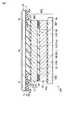
図2は、図1に示した表示パネルPNLを含む表示装置DSPの断面を概略的に示す断面図である。 FIG. 2 is a cross-sectional view schematically showing a cross section of the display device DSP including the display panel PNL shown in FIG.
表示装置DSPは、表示モジュールMDLと、カバー部材CBと、表示モジュールMDLとカバー部材CBとを接着する接着剤PSと、を備えている。 The display device DSP includes a display module MDL, a cover member CB, and an adhesive PS that bonds the display module MDL and the cover member CB.
表示モジュールMDLは、表示パネルPNL、第1光学素子OD1、第2光学素子OD2、及び、バックライトBLを備えている。 The display module MDL includes a display panel PNL, a first optical element OD1, a second optical element OD2, and a backlight BL.
本実施形態の表示パネルPNLは、例えば液晶パネルであり、アレイ基板ARと対向基板CTとの間に液晶層LQを保持している。アレイ基板ARと対向基板CTとは、シール材SEによって貼り合わせられている。アレイ基板ARについて、対向基板CTと向かい合う内面側の構造については詳細な説明を省略する。対向基板CTについて、アレイ基板ARと向かい合う内面側の構造については詳細な説明を省略するが、周辺エリアPRPに周辺遮光層SHDが形成されている。この周辺遮光層SHDは、アクティブエリアACTの周囲に形成されており、詳述しないが、アクティブエリアACTを囲む矩形枠状に形成されている。 The display panel PNL of this embodiment is a liquid crystal panel, for example, and holds a liquid crystal layer LQ between the array substrate AR and the counter substrate CT. The array substrate AR and the counter substrate CT are bonded together with a seal material SE. A detailed description of the structure of the inner surface of the array substrate AR facing the counter substrate CT will be omitted. Although the detailed description of the structure of the counter substrate CT on the inner surface facing the array substrate AR is omitted, a peripheral light shielding layer SHD is formed in the peripheral area PRP. The peripheral light shielding layer SHD is formed around the active area ACT, and is formed in a rectangular frame shape surrounding the active area ACT, although not described in detail.
第1光学素子OD1は、バックライトBLと対向するアレイ基板ARの外面に接着されている。第1光学素子OD1は、第1偏光板PL1を含んでいる。第1光学素子OD1は、アクティブエリアACTの全体を覆うように配置され、その端部は周辺エリアPRPに位置している。 The first optical element OD1 is bonded to the outer surface of the array substrate AR facing the backlight BL. The first optical element OD1 includes a first polarizing plate PL1. The first optical element OD1 is arranged so as to cover the entire active area ACT, and its end is located in the peripheral area PRP.
第2光学素子OD2は、カバー部材CBと対向する対向基板CTの外面に接着されている。第2光学素子OD2は、第2偏光板PL2を含んでいる。第2光学素子OD2は、アクティブエリアACTの全体を覆うように配置され、その端部ODEは周辺エリアPRPに位置している。なお、第1光学素子OD1及び第2光学素子OD2は、それぞれ必要に応じて、位相差板などの各種光学部材を含んでいても良い。 The second optical element OD2 is bonded to the outer surface of the counter substrate CT facing the cover member CB. The second optical element OD2 includes a second polarizing plate PL2. The second optical element OD2 is disposed so as to cover the entire active area ACT, and its end ODE is located in the peripheral area PRP. Note that the first optical element OD1 and the second optical element OD2 may each include various optical members such as a retardation plate, as necessary.
バックライトBLは、表示パネルPNLの背面側に配置されている。バックライトBLとしては、種々の形態が適用可能であり、また、光源として発光ダイオード(LED)を利用したものや冷陰極管(CCFL)を利用したものなどのいずれでも適用可能であり、詳細な構造については説明を省略する。なお、バックライトBLは、表示パネルPNLと一体化されていても良い。 The backlight BL is disposed on the back side of the display panel PNL. As the backlight BL, various forms are applicable, and any of those using a light emitting diode (LED) or a cold cathode tube (CCFL) as a light source can be applied. The description of the structure is omitted. Note that the backlight BL may be integrated with the display panel PNL.
カバー部材CBは、表示モジュールMDLの前面側(あるいは表示面側)に配置され、第2光学素子OD2と対向している。このカバー部材CBは、透過部TRと、額縁部FRと、を備えている。透過部TRは、透明であり、表示パネルPNLのアクティブエリアACTに対向している。額縁部FRは、透過部TRの外側に位置しており、透過部TRを囲み、表示パネルPNLの周辺エリアPRPに対向している。また、額縁部FRには、周辺エリアPRPと対向する溝GRが形成されている。 The cover member CB is disposed on the front surface side (or display surface side) of the display module MDL and faces the second optical element OD2. The cover member CB includes a transmission part TR and a frame part FR. The transmission part TR is transparent and faces the active area ACT of the display panel PNL. The frame portion FR is located outside the transmissive portion TR, surrounds the transmissive portion TR, and faces the peripheral area PRP of the display panel PNL. In addition, a groove GR that faces the peripheral area PRP is formed in the frame portion FR.
図示した例では、カバー部材CBは、透明な基材10と、着色層11と、を備えている。基材10は、透明なガラス板やプラスチック板などであり、透過部TR及び額縁部FRに亘って延在している。着色層11は、額縁部FRにおける基材10の内面10A(つまり表示パネルPNLと対向する側)に形成されている。この着色層11は、例えば黒色に着色された樹脂材料によって形成されている。
In the illustrated example, the cover member CB includes a
溝GRは、着色層11に形成されている。この溝GRは、透過部TRの周囲に形成されるものであって、詳細な形状については後述するが、図示した断面においては、内面10Aに至るまで着色層11を貫通せず、着色層11の膜厚よりも浅い深さとなるように形成されている。つまり、溝GRが着色層11に形成された本構成例において、額縁部FRの略全体は着色層11によって覆われており、溝GRがカバー部材CBの前面側から目視されることはない。
The groove GR is formed in the
接着剤PSは、第2光学素子OD2とカバー部材CBとを接着している。すなわち、接着剤PSは、第2光学素子OD2の表面に接しているとともに、カバー部材CBの透過部TRでは基材10の内面10Aに接し、また、額縁部FRにおいては着色層11に接し、溝GRにも入り込んでいる。この接着剤PSは、透明であり、アクティブエリアACTにおける表示の妨げとはならない。接着剤PSの端部PSEは、表示パネルPNLの周辺エリアPRP、あるいは、カバー部材CBの額縁部FRと重なる位置にあるが、第2光学素子OD2の端部ODEを露出している。つまり、接着剤PSは、端部ODEを覆っていない。このような接着剤PSは、感光性樹脂、例えば、紫外線照射によって硬化する紫外線硬化型の樹脂材料などによって形成されている。
The adhesive PS bonds the second optical element OD2 and the cover member CB. That is, the adhesive PS is in contact with the surface of the second optical element OD2, is in contact with the
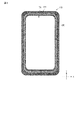
図3は、図2に示したカバー部材CBの一例を示す平面図である。 FIG. 3 is a plan view showing an example of the cover member CB shown in FIG.
カバー部材CBは、例えば、第1方向Xに一対の短辺を有するとともに第2方向Yに一対の長辺を有する略長方形状である。透過部TRは、カバー部材CBの中央部に位置しており、その形状はアクティブエリアACTの形状にほぼ対応している。額縁部FRは、透過部TRの周囲に連続的に形成された枠状である。 The cover member CB has, for example, a substantially rectangular shape having a pair of short sides in the first direction X and a pair of long sides in the second direction Y. The transmission part TR is located in the central part of the cover member CB, and its shape substantially corresponds to the shape of the active area ACT. The frame part FR has a frame shape continuously formed around the transmission part TR.
図示した例では、溝GRは、透過部TRを囲むループ状に形成されている。 In the illustrated example, the groove GR is formed in a loop shape surrounding the transmission part TR.
図4は、図2に示したカバー部材CBの他の例を示す平面図である。 FIG. 4 is a plan view showing another example of the cover member CB shown in FIG.
ここに示した例では、溝GRは、透過部TRからその外側に向かって放射状に形成されている。すなわち、カバー部材CBの長辺に沿った位置では、溝GRは、透過部TRから第1方向Xに沿って延出し、カバー部材CBの短辺に沿った位置では、溝GRは、透過部TRから第2方向Yに沿って延出し、カバー部材CBのコーナー付近では、溝GRは、透過部TRから斜め方向(あるいはカバー部材CBの対角線方向)に沿って延出している。これらの溝GRは、図示した例では、カバー部材CBの端部まで至らず、額縁部FRの途中で途切れている。 In the example shown here, the grooves GR are formed radially from the transmission part TR toward the outside thereof. That is, at the position along the long side of the cover member CB, the groove GR extends from the transmission part TR along the first direction X, and at the position along the short side of the cover member CB, the groove GR is formed at the transmission part. The groove GR extends from TR along the second direction Y, and in the vicinity of the corner of the cover member CB, the groove GR extends from the transmission portion TR along the diagonal direction (or the diagonal direction of the cover member CB). In the illustrated example, these grooves GR do not reach the end of the cover member CB, but are interrupted in the middle of the frame portion FR.
なお、溝GRの数や形状は、上記の例に限定されるものではなく、ループの一部が途切れていても良いし、2重以上のループ状に形成しても良いし、表示等に影響のないエリアなどに局所的に多くの溝GRを形成しても良いし、図示した例よりも幅広の溝GRを形成しても良い。 The number and shape of the grooves GR are not limited to the above example, and a part of the loop may be interrupted, may be formed in a double or more loop shape, or may be displayed. A large number of grooves GR may be locally formed in an unaffected area or the like, or a groove GR wider than the illustrated example may be formed.
このような構成において、表示装置DSPは、例えば、以下のように製造される。すなわち、表示パネルPNLに第1光学素子OD1及び第2光学素子OD2をそれぞれ接着した表示モジュールMDLを用意する。一方で、基材10の内面10Aに未硬化(あるいは液状)の接着剤PSを塗布する。そして、第2光学素子OD2が接着剤PSと向かい合うように、接着剤PSの上に表示モジュールMDLを載置した後、適度に加圧し、接着剤PSを押し広げる。この際、透過部TRから外側に広がった接着剤PSは、溝GRに入り込む。接着剤PSがアクティブエリアACTの全域をカバーするように広がった後、ハロゲンランプなどの紫外線硬化用光源からの紫外線をカバー部材CBの前面側などから照射する。これにより、接着剤PSが硬化し、表示モジュールMDLとカバー部材CBとを接着した表示装置DSPが製造される。
In such a configuration, the display device DSP is manufactured as follows, for example. That is, the display module MDL is prepared by bonding the first optical element OD1 and the second optical element OD2 to the display panel PNL. On the other hand, an uncured (or liquid) adhesive PS is applied to the
このような本実施形態によれば、表示装置DSPの製造過程で広がった接着剤PSによる第2光学素子OD2の汚染を抑制することが可能となる。すなわち、第2光学素子OD2は、第2偏光板PL2を含む積層体として構成されている。一例では、第2光学素子OD2は、一対の支持層の間に偏光子層を挟持した構成の第2偏光板PL2を含んでおり、各層が互いに接着されている。また、第2光学素子OD2では、一方の支持層の裏面にさらに位相差フィルムが接着されている場合もあり得る。このような積層体からなる第2光学素子OD2において、その端部ODEが接着剤PSに触れると、接着剤PSの主成分である樹脂材料が端部ODEから積層体の層間にしみ込み、第2光学素子OD2の外形が変形してしまったり、積層体の層間が分離してしまったり、第2光学素子OD2が表示パネルPNLから浮き上がってしまったりする。このような第2光学素子OD2の汚染の影響がアクティブエリアACTを覆っている部分まで及んだ場合には、表示ムラなどの表示品位の劣化を招くおそれがある。本実施形態では、製造過程で広がった接着剤PSは、カバー部材CBに形成された溝GRに誘導されるため、第2光学素子OD2の端部ODEへの接着剤PSの接触を避けることが可能となる。このため、第2光学素子OD2の汚染による不具合、つまり、第2光学素子OD2の変形や層間の分離、表示パネルPNLからの浮き上がりを抑制することが可能となる。したがって、信頼性の低下あるいは表示品位の劣化などの品質の劣化を抑制することが可能となる。 According to this embodiment as described above, it is possible to suppress the contamination of the second optical element OD2 due to the adhesive PS that has spread in the manufacturing process of the display device DSP. That is, the second optical element OD2 is configured as a laminate including the second polarizing plate PL2. In one example, the second optical element OD2 includes a second polarizing plate PL2 having a configuration in which a polarizer layer is sandwiched between a pair of support layers, and the layers are bonded to each other. In the second optical element OD2, there may be a case where a retardation film is further adhered to the back surface of one of the support layers. In the second optical element OD2 composed of such a laminate, when the end portion ODE touches the adhesive PS, the resin material that is the main component of the adhesive PS penetrates into the interlayer of the laminate from the end portion ODE. The outer shape of the second optical element OD2 may be deformed, the layers of the laminate may be separated, and the second optical element OD2 may be lifted from the display panel PNL. When the influence of the contamination of the second optical element OD2 reaches the portion covering the active area ACT, there is a risk of causing display quality deterioration such as display unevenness. In the present embodiment, since the adhesive PS spread in the manufacturing process is guided to the groove GR formed in the cover member CB, the contact of the adhesive PS with the end portion ODE of the second optical element OD2 is avoided. It becomes possible. For this reason, it is possible to suppress problems due to contamination of the second optical element OD2, that is, deformation of the second optical element OD2, separation between layers, and lifting from the display panel PNL. Therefore, it is possible to suppress deterioration in quality such as a decrease in reliability or display quality.
また、カバー部材CBに溝GRを形成したことにより、カバー部材CBと表示モジュールMDLとを接着する際に、溝GRを目印(アライメントマーク)として利用することが可能となる。このため、別途アライメントマークを設けなくても、接着の際の合わせ精度を向上することが可能となる。 Further, since the groove GR is formed in the cover member CB, the groove GR can be used as a mark (alignment mark) when the cover member CB and the display module MDL are bonded. For this reason, it is possible to improve the alignment accuracy at the time of bonding without separately providing an alignment mark.
また、溝GRは過剰に塗布された接着剤PSの受け皿となるため、接着剤PSの塗布量のマージンを拡大することが可能となる。 Further, since the groove GR serves as a tray for the adhesive PS applied excessively, it is possible to expand the margin of the application amount of the adhesive PS.
なお、上記のカバー部材CBは、タッチパネルを含んでいても良いし、基材10がタッチパネルを構成する基板であっても良い。
In addition, said cover member CB may contain the touch panel and the
次に、他の構成例について説明する。 Next, another configuration example will be described.
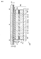
図5は、本実施形態の表示装置DSPの他の構成例を概略的に示す断面図である。 FIG. 5 is a cross-sectional view schematically showing another configuration example of the display device DSP of the present embodiment.
図示した構成例は、図2に示した構成例と比較して、カバー部材CBがさらにオーバーコート層12を備えている点で相違している。
The illustrated configuration example is different from the configuration example illustrated in FIG. 2 in that the cover member CB further includes an
すなわち、カバー部材CBは、透過部TR及び額縁部FRに亘って延在する基材10と、額縁部FRにおける基材10の内面10Aに形成された着色層11と、透過部TRにおける基材10の内面10Aに形成されるとともに着色層11を覆うオーバーコート層12と、を備えている。オーバーコート層12は、例えば、透明な樹脂材料によって形成され、内面10Aと着色層11との段差を平坦化する。額縁部FRに位置する溝GRは、オーバーコート層12に形成されている。
That is, the cover member CB includes the
接着剤PSは、第2光学素子OD2とオーバーコート層12との間に介在している。接着剤PSの一部は、溝GRに入り込み、第2光学素子OD2の端部ODEにはほとんど接触していない。
The adhesive PS is interposed between the second optical element OD2 and the
このような構成例においても、上記の構成例と同様の効果が得られる。 Also in such a configuration example, the same effect as the above configuration example can be obtained.
図6は、本実施形態の表示装置DSPの他の構成例を概略的に示す断面図である。 FIG. 6 is a cross-sectional view schematically showing another configuration example of the display device DSP of the present embodiment.
図示した構成例は、図2に示した構成例と比較して、カバー部材CBが着色層11を省略した点で相違している。
The illustrated configuration example is different from the configuration example illustrated in FIG. 2 in that the cover member CB omits the
すなわち、カバー部材CBは、透過部TR及び額縁部FRに亘って延在する基材10を備えている。額縁部FRに位置する溝GRは、基材10の表示モジュールMDLと対向する側に形成されている。なお、基材10は、額縁部FRにおいて黒化処理されるなどして着色されていても良い。
That is, the cover member CB includes the
接着剤PSは、第2光学素子OD2と基材10との間に介在している。接着剤PSの一部は、溝GRに入り込み、第2光学素子OD2の端部ODEにはほとんど接触していない。
The adhesive PS is interposed between the second optical element OD2 and the
このような構成例においても、上記の構成例と同様の効果が得られる。 Also in such a configuration example, the same effect as the above configuration example can be obtained.
以上説明したように、本実施形態によれば、品質の劣化を抑制することが可能な表示装置を提供することができる。 As described above, according to the present embodiment, it is possible to provide a display device capable of suppressing deterioration in quality.
なお、本発明のいくつかの実施形態を説明したが、これらの実施形態は、例として提示したものであり、発明の範囲を限定することは意図していない。これらの新規な実施形態は、その他の様々な形態で実施されることが可能であり、発明の要旨を逸脱しない範囲で、種々の省略、置き換え、変更を行うことができる。これらの実施形態やその変形は、発明の範囲や要旨に含まれるとともに、特許請求の範囲に記載された発明とその均等の範囲に含まれる。 In addition, although some embodiment of this invention was described, these embodiment is shown as an example and is not intending limiting the range of invention. These novel embodiments can be implemented in various other forms, and various omissions, replacements, and changes can be made without departing from the spirit of the invention. These embodiments and modifications thereof are included in the scope and gist of the invention, and are included in the invention described in the claims and the equivalents thereof.
DSP…表示装置
MDL…表示モジュール
PNL…表示パネル AR…アレイ基板 CT…対向基板 LQ…液晶層
ACT…アクティブエリア PRP…周辺エリア
OD1…第1光学素子 OD2…第2光学素子
CB…カバー部材
TR…透過部 FR…額縁部 GR…溝
10…基材 11…着色層 12…オーバーコート層
PS…接着剤
DSP ... Display device MDL ... Display module PNL ... Display panel AR ... Array substrate CT ... Opposite substrate LQ ... Liquid crystal layer ACT ... Active area PRP ... Peripheral area OD1 ... First optical element OD2 ... Second optical element CB ... Cover member TR ... Transmission part FR ... Frame part GR ...
Claims (6)
前記アクティブエリアと対向する透過部と、前記透過部を囲み前記周辺エリアと対向する溝が形成された額縁部と、を備えたカバー部材と、
前記表示パネルの前記カバー部材と対向する外面に接着され、前記アクティブエリアを覆う光学素子と、
前記光学素子と前記カバー部材とを接着する接着剤と、
を備えた、表示装置。 A display panel comprising an active area for displaying an image, and a peripheral area surrounding the active area;
A cover member comprising: a transmissive portion facing the active area; and a frame portion surrounding the transmissive portion and formed with a groove facing the peripheral area;
An optical element bonded to an outer surface of the display panel facing the cover member and covering the active area;
An adhesive that bonds the optical element and the cover member;
A display device comprising:
前記溝は、前記着色層に形成された、請求項1乃至3のいずれか1項に記載の表示装置。 The cover member includes a base material extending over the transmission part and the frame part, and a colored layer formed on an inner surface of the base part facing the display panel of the base part,
The display device according to claim 1, wherein the groove is formed in the colored layer.
前記溝は、前記オーバーコート層に形成された、請求項1乃至3のいずれか1項に記載の表示装置。 The cover member includes a base material extending over the transmission part and the frame part, a colored layer formed on an inner surface of the base part facing the display panel of the base part, and the transmission part in the transmission part. An overcoat layer that is formed on the inner surface of the substrate and covers the colored layer,
The display device according to claim 1, wherein the groove is formed in the overcoat layer.
前記溝は、前記基材に形成された、請求項1乃至3のいずれか1項に記載の表示装置。 The cover member includes a base material extending over the transmission part and the frame part,
The display device according to claim 1, wherein the groove is formed in the base material.
Priority Applications (1)
| Application Number | Priority Date | Filing Date | Title |
|---|---|---|---|
| JP2012266148A JP2014112139A (en) | 2012-12-05 | 2012-12-05 | Display device |
Applications Claiming Priority (1)
| Application Number | Priority Date | Filing Date | Title |
|---|---|---|---|
| JP2012266148A JP2014112139A (en) | 2012-12-05 | 2012-12-05 | Display device |
Publications (2)
| Publication Number | Publication Date |
|---|---|
| JP2014112139A true JP2014112139A (en) | 2014-06-19 |
| JP2014112139A5 JP2014112139A5 (en) | 2016-01-28 |
Family
ID=51169324
Family Applications (1)
| Application Number | Title | Priority Date | Filing Date |
|---|---|---|---|
| JP2012266148A Pending JP2014112139A (en) | 2012-12-05 | 2012-12-05 | Display device |
Country Status (1)
| Country | Link |
|---|---|
| JP (1) | JP2014112139A (en) |
Cited By (4)
| Publication number | Priority date | Publication date | Assignee | Title |
|---|---|---|---|---|
| JP6081032B1 (en) * | 2015-12-01 | 2017-02-15 | 三菱電機株式会社 | Display device |
| KR20180034772A (en) * | 2016-09-27 | 2018-04-05 | 삼성디스플레이 주식회사 | Display device |
| JP2019066669A (en) * | 2017-09-29 | 2019-04-25 | シチズンファインデバイス株式会社 | Manufacturing method for image display device |
| JP2020008758A (en) * | 2018-07-10 | 2020-01-16 | 三菱電機株式会社 | Display device |
Citations (7)
| Publication number | Priority date | Publication date | Assignee | Title |
|---|---|---|---|---|
| JPH0836151A (en) * | 1994-07-22 | 1996-02-06 | Nippon Sheet Glass Co Ltd | Laminating method of planer substrate |
| JPH08114770A (en) * | 1994-08-26 | 1996-05-07 | Omron Corp | Optical low-pass filter and dot matrix display device utilizing the same |
| JP2008009189A (en) * | 2006-06-29 | 2008-01-17 | Sharp Corp | Display device |
| JP2008292883A (en) * | 2007-05-28 | 2008-12-04 | Hitachi Displays Ltd | Image display device |
| WO2010116569A1 (en) * | 2009-04-07 | 2010-10-14 | シャープ株式会社 | Display device and method for manufacturing same |
| JP2011209590A (en) * | 2010-03-30 | 2011-10-20 | Casio Computer Co Ltd | Display module |
| JP2012230304A (en) * | 2011-04-27 | 2012-11-22 | Yamaguchi Tokushu Insatsu:Kk | Method for manufacturing protective sheet for liquid crystal display, protective sheet for liquid crystal display, method for manufacturing liquid crystal display device and liquid crystal display device |
-
2012
- 2012-12-05 JP JP2012266148A patent/JP2014112139A/en active Pending
Patent Citations (7)
| Publication number | Priority date | Publication date | Assignee | Title |
|---|---|---|---|---|
| JPH0836151A (en) * | 1994-07-22 | 1996-02-06 | Nippon Sheet Glass Co Ltd | Laminating method of planer substrate |
| JPH08114770A (en) * | 1994-08-26 | 1996-05-07 | Omron Corp | Optical low-pass filter and dot matrix display device utilizing the same |
| JP2008009189A (en) * | 2006-06-29 | 2008-01-17 | Sharp Corp | Display device |
| JP2008292883A (en) * | 2007-05-28 | 2008-12-04 | Hitachi Displays Ltd | Image display device |
| WO2010116569A1 (en) * | 2009-04-07 | 2010-10-14 | シャープ株式会社 | Display device and method for manufacturing same |
| JP2011209590A (en) * | 2010-03-30 | 2011-10-20 | Casio Computer Co Ltd | Display module |
| JP2012230304A (en) * | 2011-04-27 | 2012-11-22 | Yamaguchi Tokushu Insatsu:Kk | Method for manufacturing protective sheet for liquid crystal display, protective sheet for liquid crystal display, method for manufacturing liquid crystal display device and liquid crystal display device |
Cited By (12)
| Publication number | Priority date | Publication date | Assignee | Title |
|---|---|---|---|---|
| JP6081032B1 (en) * | 2015-12-01 | 2017-02-15 | 三菱電機株式会社 | Display device |
| WO2017094125A1 (en) * | 2015-12-01 | 2017-06-08 | 三菱電機株式会社 | Display protection sheet and display device |
| CN108292482A (en) * | 2015-12-01 | 2018-07-17 | 三菱电机株式会社 | Display screening glass and display device |
| CN108292482B (en) * | 2015-12-01 | 2019-03-01 | 三菱电机株式会社 | Display device |
| KR20180034772A (en) * | 2016-09-27 | 2018-04-05 | 삼성디스플레이 주식회사 | Display device |
| JP2018055099A (en) * | 2016-09-27 | 2018-04-05 | 三星ディスプレイ株式會社Samsung Display Co.,Ltd. | Display device |
| JP7010639B2 (en) | 2016-09-27 | 2022-01-26 | 三星ディスプレイ株式會社 | Display device |
| US11502007B2 (en) | 2016-09-27 | 2022-11-15 | Samsung Display Co., Ltd. | Display device including an adhesive layer |
| KR102632168B1 (en) * | 2016-09-27 | 2024-02-01 | 삼성디스플레이 주식회사 | Display device |
| JP2019066669A (en) * | 2017-09-29 | 2019-04-25 | シチズンファインデバイス株式会社 | Manufacturing method for image display device |
| JP2020008758A (en) * | 2018-07-10 | 2020-01-16 | 三菱電機株式会社 | Display device |
| US11874544B2 (en) | 2018-07-10 | 2024-01-16 | Trivale Technologies | Display device |
Similar Documents
| Publication | Publication Date | Title |
|---|---|---|
| JP2014056222A (en) | Display device and cover member | |
| US10495803B2 (en) | Display device | |
| US10001676B2 (en) | Display device | |
| US9285637B2 (en) | Liquid-crystal display | |
| TW201814464A (en) | Display device | |
| JP5923417B2 (en) | Display device and cover member | |
| JP2014122947A (en) | Display device and cover member | |
| JP2009069321A (en) | Display device | |
| JP5553648B2 (en) | Display device | |
| JP2018054733A (en) | Liquid crystal display device and color filter substrate | |
| JP5905173B1 (en) | Liquid crystal display | |
| JP2020027190A (en) | Display device | |
| JP2014157311A (en) | Display device and manufacturing method of display device | |
| US10234730B2 (en) | Liquid crystal display device | |
| JP2014235185A (en) | Display device | |
| JP2014013266A (en) | Display device, and manufacturing method therefor | |
| US20170357123A1 (en) | Liquid crystal display module and method for fabricating the same, display device | |
| JP2015022120A (en) | Display element and manufacturing method of the same | |
| JP2015079235A (en) | Display device | |
| WO2013161686A1 (en) | Method for manufacturing display device | |
| JP2014112139A (en) | Display device | |
| WO2012161109A1 (en) | Liquid crystal element and display device | |
| US20160231774A1 (en) | Display module | |
| JP2017058394A (en) | Display device and method for manufacturing display device | |
| JP2016157072A (en) | Display |
Legal Events
| Date | Code | Title | Description |
|---|---|---|---|
| A521 | Request for written amendment filed |
Free format text: JAPANESE INTERMEDIATE CODE: A523 Effective date: 20151201 |
|
| A621 | Written request for application examination |
Free format text: JAPANESE INTERMEDIATE CODE: A621 Effective date: 20151201 |
|
| A977 | Report on retrieval |
Free format text: JAPANESE INTERMEDIATE CODE: A971007 Effective date: 20160928 |
|
| A131 | Notification of reasons for refusal |
Free format text: JAPANESE INTERMEDIATE CODE: A131 Effective date: 20161004 |
|
| A521 | Request for written amendment filed |
Free format text: JAPANESE INTERMEDIATE CODE: A523 Effective date: 20161201 |
|
| A02 | Decision of refusal |
Free format text: JAPANESE INTERMEDIATE CODE: A02 Effective date: 20170509 |