JP2014123718A - Magnetic sheet, method for manufacturing magnetic sheet, and contactless power charger including magnetic sheet - Google Patents
Magnetic sheet, method for manufacturing magnetic sheet, and contactless power charger including magnetic sheet Download PDFInfo
- Publication number
- JP2014123718A JP2014123718A JP2013238829A JP2013238829A JP2014123718A JP 2014123718 A JP2014123718 A JP 2014123718A JP 2013238829 A JP2013238829 A JP 2013238829A JP 2013238829 A JP2013238829 A JP 2013238829A JP 2014123718 A JP2014123718 A JP 2014123718A
- Authority
- JP
- Japan
- Prior art keywords
- magnetic sheet
- insulating layer
- manufacturing
- present
- metal
- Prior art date
- Legal status (The legal status is an assumption and is not a legal conclusion. Google has not performed a legal analysis and makes no representation as to the accuracy of the status listed.)
- Pending
Links
Images

Classifications
-
- B—PERFORMING OPERATIONS; TRANSPORTING
- B32—LAYERED PRODUCTS
- B32B—LAYERED PRODUCTS, i.e. PRODUCTS BUILT-UP OF STRATA OF FLAT OR NON-FLAT, e.g. CELLULAR OR HONEYCOMB, FORM
- B32B15/00—Layered products comprising a layer of metal
- B32B15/04—Layered products comprising a layer of metal comprising metal as the main or only constituent of a layer, which is next to another layer of the same or of a different material
- B32B15/08—Layered products comprising a layer of metal comprising metal as the main or only constituent of a layer, which is next to another layer of the same or of a different material of synthetic resin
-
- H—ELECTRICITY
- H01—ELECTRIC ELEMENTS
- H01F—MAGNETS; INDUCTANCES; TRANSFORMERS; SELECTION OF MATERIALS FOR THEIR MAGNETIC PROPERTIES
- H01F38/00—Adaptations of transformers or inductances for specific applications or functions
- H01F38/14—Inductive couplings
-
- B—PERFORMING OPERATIONS; TRANSPORTING
- B22—CASTING; POWDER METALLURGY
- B22F—WORKING METALLIC POWDER; MANUFACTURE OF ARTICLES FROM METALLIC POWDER; MAKING METALLIC POWDER; APPARATUS OR DEVICES SPECIALLY ADAPTED FOR METALLIC POWDER
- B22F10/00—Additive manufacturing of workpieces or articles from metallic powder
- B22F10/10—Formation of a green body
-
- B—PERFORMING OPERATIONS; TRANSPORTING
- B22—CASTING; POWDER METALLURGY
- B22F—WORKING METALLIC POWDER; MANUFACTURE OF ARTICLES FROM METALLIC POWDER; MAKING METALLIC POWDER; APPARATUS OR DEVICES SPECIALLY ADAPTED FOR METALLIC POWDER
- B22F7/00—Manufacture of composite layers, workpieces, or articles, comprising metallic powder, by sintering the powder, with or without compacting wherein at least one part is obtained by sintering or compression
- B22F7/02—Manufacture of composite layers, workpieces, or articles, comprising metallic powder, by sintering the powder, with or without compacting wherein at least one part is obtained by sintering or compression of composite layers
-
- H—ELECTRICITY
- H01—ELECTRIC ELEMENTS
- H01F—MAGNETS; INDUCTANCES; TRANSFORMERS; SELECTION OF MATERIALS FOR THEIR MAGNETIC PROPERTIES
- H01F10/00—Thin magnetic films, e.g. of one-domain structure
- H01F10/08—Thin magnetic films, e.g. of one-domain structure characterised by magnetic layers
- H01F10/10—Thin magnetic films, e.g. of one-domain structure characterised by magnetic layers characterised by the composition
- H01F10/12—Thin magnetic films, e.g. of one-domain structure characterised by magnetic layers characterised by the composition being metals or alloys
-
- H—ELECTRICITY
- H01—ELECTRIC ELEMENTS
- H01F—MAGNETS; INDUCTANCES; TRANSFORMERS; SELECTION OF MATERIALS FOR THEIR MAGNETIC PROPERTIES
- H01F10/00—Thin magnetic films, e.g. of one-domain structure
- H01F10/26—Thin magnetic films, e.g. of one-domain structure characterised by the substrate or intermediate layers
- H01F10/265—Magnetic multilayers non exchange-coupled
-
- H—ELECTRICITY
- H01—ELECTRIC ELEMENTS
- H01F—MAGNETS; INDUCTANCES; TRANSFORMERS; SELECTION OF MATERIALS FOR THEIR MAGNETIC PROPERTIES
- H01F27/00—Details of transformers or inductances, in general
- H01F27/34—Special means for preventing or reducing unwanted electric or magnetic effects, e.g. no-load losses, reactive currents, harmonics, oscillations, leakage fields
- H01F27/36—Electric or magnetic shields or screens
- H01F27/363—Electric or magnetic shields or screens made of electrically conductive material
-
- H—ELECTRICITY
- H01—ELECTRIC ELEMENTS
- H01F—MAGNETS; INDUCTANCES; TRANSFORMERS; SELECTION OF MATERIALS FOR THEIR MAGNETIC PROPERTIES
- H01F41/00—Apparatus or processes specially adapted for manufacturing or assembling magnets, inductances or transformers; Apparatus or processes specially adapted for manufacturing materials characterised by their magnetic properties
- H01F41/32—Apparatus or processes specially adapted for manufacturing or assembling magnets, inductances or transformers; Apparatus or processes specially adapted for manufacturing materials characterised by their magnetic properties for applying conductive, insulating or magnetic material on a magnetic film, specially adapted for a thin magnetic film
-
- H—ELECTRICITY
- H02—GENERATION; CONVERSION OR DISTRIBUTION OF ELECTRIC POWER
- H02J—ELECTRIC POWER NETWORKS; CIRCUIT ARRANGEMENTS OR SYSTEMS FOR SUPPLYING OR DISTRIBUTING ELECTRIC POWER; SYSTEMS FOR STORING ELECTRIC ENERGY
- H02J50/00—Circuit arrangements or systems for wireless supply or distribution of electric power
- H02J50/005—Mechanical details of housing or structure aiming to accommodate the power transfer means, e.g. mechanical integration of coils, antennas or transducers into emitting or receiving devices
-
- H—ELECTRICITY
- H02—GENERATION; CONVERSION OR DISTRIBUTION OF ELECTRIC POWER
- H02J—ELECTRIC POWER NETWORKS; CIRCUIT ARRANGEMENTS OR SYSTEMS FOR SUPPLYING OR DISTRIBUTING ELECTRIC POWER; SYSTEMS FOR STORING ELECTRIC ENERGY
- H02J50/00—Circuit arrangements or systems for wireless supply or distribution of electric power
- H02J50/70—Circuit arrangements or systems for wireless supply or distribution of electric power involving the reduction of electric, magnetic or electromagnetic leakage fields
-
- C—CHEMISTRY; METALLURGY
- C22—METALLURGY; FERROUS OR NON-FERROUS ALLOYS; TREATMENT OF ALLOYS OR NON-FERROUS METALS
- C22C—ALLOYS
- C22C2202/00—Physical properties
- C22C2202/02—Magnetic
-
- H—ELECTRICITY
- H01—ELECTRIC ELEMENTS
- H01F—MAGNETS; INDUCTANCES; TRANSFORMERS; SELECTION OF MATERIALS FOR THEIR MAGNETIC PROPERTIES
- H01F27/00—Details of transformers or inductances, in general
- H01F27/28—Coils; Windings; Conductive connections
- H01F27/2871—Pancake coils
-
- H—ELECTRICITY
- H02—GENERATION; CONVERSION OR DISTRIBUTION OF ELECTRIC POWER
- H02J—ELECTRIC POWER NETWORKS; CIRCUIT ARRANGEMENTS OR SYSTEMS FOR SUPPLYING OR DISTRIBUTING ELECTRIC POWER; SYSTEMS FOR STORING ELECTRIC ENERGY
- H02J50/00—Circuit arrangements or systems for wireless supply or distribution of electric power
- H02J50/10—Circuit arrangements or systems for wireless supply or distribution of electric power using inductive coupling
-
- Y—GENERAL TAGGING OF NEW TECHNOLOGICAL DEVELOPMENTS; GENERAL TAGGING OF CROSS-SECTIONAL TECHNOLOGIES SPANNING OVER SEVERAL SECTIONS OF THE IPC; TECHNICAL SUBJECTS COVERED BY FORMER USPC CROSS-REFERENCE ART COLLECTIONS [XRACs] AND DIGESTS
- Y02—TECHNOLOGIES OR APPLICATIONS FOR MITIGATION OR ADAPTATION AGAINST CLIMATE CHANGE
- Y02P—CLIMATE CHANGE MITIGATION TECHNOLOGIES IN THE PRODUCTION OR PROCESSING OF GOODS
- Y02P10/00—Technologies related to metal processing
- Y02P10/25—Process efficiency
-
- Y—GENERAL TAGGING OF NEW TECHNOLOGICAL DEVELOPMENTS; GENERAL TAGGING OF CROSS-SECTIONAL TECHNOLOGIES SPANNING OVER SEVERAL SECTIONS OF THE IPC; TECHNICAL SUBJECTS COVERED BY FORMER USPC CROSS-REFERENCE ART COLLECTIONS [XRACs] AND DIGESTS
- Y10—TECHNICAL SUBJECTS COVERED BY FORMER USPC
- Y10T—TECHNICAL SUBJECTS COVERED BY FORMER US CLASSIFICATION
- Y10T156/00—Adhesive bonding and miscellaneous chemical manufacture
- Y10T156/10—Methods of surface bonding and/or assembly therefor
-
- Y—GENERAL TAGGING OF NEW TECHNOLOGICAL DEVELOPMENTS; GENERAL TAGGING OF CROSS-SECTIONAL TECHNOLOGIES SPANNING OVER SEVERAL SECTIONS OF THE IPC; TECHNICAL SUBJECTS COVERED BY FORMER USPC CROSS-REFERENCE ART COLLECTIONS [XRACs] AND DIGESTS
- Y10—TECHNICAL SUBJECTS COVERED BY FORMER USPC
- Y10T—TECHNICAL SUBJECTS COVERED BY FORMER US CLASSIFICATION
- Y10T428/00—Stock material or miscellaneous articles
- Y10T428/24—Structurally defined web or sheet [e.g., overall dimension, etc.]
- Y10T428/24942—Structurally defined web or sheet [e.g., overall dimension, etc.] including components having same physical characteristic in differing degree
- Y10T428/2495—Thickness [relative or absolute]
- Y10T428/24967—Absolute thicknesses specified
- Y10T428/24975—No layer or component greater than 5 mils thick
-
- Y—GENERAL TAGGING OF NEW TECHNOLOGICAL DEVELOPMENTS; GENERAL TAGGING OF CROSS-SECTIONAL TECHNOLOGIES SPANNING OVER SEVERAL SECTIONS OF THE IPC; TECHNICAL SUBJECTS COVERED BY FORMER USPC CROSS-REFERENCE ART COLLECTIONS [XRACs] AND DIGESTS
- Y10—TECHNICAL SUBJECTS COVERED BY FORMER USPC
- Y10T—TECHNICAL SUBJECTS COVERED BY FORMER US CLASSIFICATION
- Y10T428/00—Stock material or miscellaneous articles
- Y10T428/31504—Composite [nonstructural laminate]
- Y10T428/31678—Of metal
Landscapes
- Engineering & Computer Science (AREA)
- Power Engineering (AREA)
- Manufacturing & Machinery (AREA)
- Chemical & Material Sciences (AREA)
- Materials Engineering (AREA)
- Computer Networks & Wireless Communication (AREA)
- Physics & Mathematics (AREA)
- Electromagnetism (AREA)
- Composite Materials (AREA)
- Mechanical Engineering (AREA)
- Laminated Bodies (AREA)
- Thin Magnetic Films (AREA)
Abstract
Description
本発明は、磁性体シート、磁性体シートの製造方法及び磁性体シートを含む無接点電力充電装置に関する。 The present invention relates to a magnetic sheet, a method for manufacturing a magnetic sheet, and a contactless power charging device including the magnetic sheet.
近年、携帯端末等に内蔵される2次電池を充電するために、電力を無接点で伝送するシステムが研究されている。 In recent years, in order to charge a secondary battery built in a portable terminal or the like, a system that transmits power in a contactless manner has been studied.
通常、無接点電力伝送装置は、電力を伝送する無接点電力送信装置と、電力を受信して貯蔵する無接点電力受信装置と、を含む。 Usually, the non-contact power transmission device includes a non-contact power transmission device that transmits power and a non-contact power reception device that receives and stores power.
上記無接点電力伝送装置は、電磁誘導を用いて電力を送受信するためにそれぞれの内部にコイルが備えられる。 The non-contact power transmission device includes a coil inside each for transmitting and receiving power using electromagnetic induction.
回路部とコイル部で構成された無接点電力受信装置の場合、携帯電話ケース又はクレードル(cradle)型のアクセサリー機器に付着されてその機能を発現する。 In the case of a non-contact power receiving apparatus configured by a circuit unit and a coil unit, it is attached to a mobile phone case or a cradle type accessory device to exhibit its function.
無接点電力伝送装置の作動原理は下記の通りである。まず、無接点電力送信装置の電源部に外部からの家庭用交流電源が入力される。 The operation principle of the non-contact power transmission device is as follows. First, an external household AC power supply is input to the power supply unit of the non-contact power transmission apparatus.
その後、入力された家庭用交流電源が電源変換部で直流電源に変換され、再度特定周波数の交流電圧に変換されて無接点送信装置に提供される。 Thereafter, the input household AC power is converted into a DC power by the power converter, and is converted again into an AC voltage of a specific frequency and provided to the non-contact transmitter.
次いで、交流電圧が無接点電力送信装置のコイル部に印加されてコイル部の周辺の磁場が変化する。 Next, an AC voltage is applied to the coil part of the non-contact power transmission device, and the magnetic field around the coil part changes.
無接点電力送信装置に隣接して配置される無接点電力受信装置のコイル部の磁場の変化により、無接点電力受信装置のコイル部から電源が出力されて2次電池を充電する。 Due to the change in the magnetic field of the coil portion of the non-contact power receiving device arranged adjacent to the non-contact power transmitting device, the power is output from the coil portion of the non-contact power receiving device to charge the secondary battery.
上記無接点電力伝送装置では、通信距離の増大のためにRFアンテナと金属バッテリーの間に磁性体シートが位置する。 In the non-contact power transmission device, a magnetic sheet is positioned between the RF antenna and the metal battery in order to increase the communication distance.
従来では、金属磁性体である軟磁性金属粉末をミリング器等を用いて球形からフレーク(flake)形にした後、分散剤と樹脂を用いてシート状に成形した。 Conventionally, a soft magnetic metal powder, which is a metal magnetic material, is formed from a spherical shape into a flake shape using a milling machine or the like, and then formed into a sheet shape using a dispersant and a resin.
上記フレーク(flake)形粉末の厚さは1μm〜2μm、長さは数十〜数百マイクロメートルであった。 The thickness of the flake powder was 1 μm to 2 μm, and the length was several tens to several hundreds of micrometers.
磁性体シートの透磁率を増加させるためには、上記フレーク形粉末の体積分率と縦横比(aspect ratio)を増加させなければならない。 In order to increase the magnetic permeability of the magnetic sheet, the volume fraction and aspect ratio of the flake powder must be increased.
したがって、高い透磁率を有する磁性体シートの製作が必要とされている。 Therefore, it is necessary to produce a magnetic sheet having a high magnetic permeability.
下記特許文献1は、積層型磁性材料に関するものである。しかしながら、上記特許文献には、本願発明のような薄膜の金属層を形成する方法が開示されていない。 The following Patent Document 1 relates to a laminated magnetic material. However, the above patent document does not disclose a method of forming a thin metal layer as in the present invention.
本発明の目的は、上述した従来技術の問題を解決することである。 The object of the present invention is to solve the above-mentioned problems of the prior art.
より具体的には、本発明の一目的は、透磁率が増加した磁性体シートの製造方法及び磁性体シートを提供することである。 More specifically, an object of the present invention is to provide a method for manufacturing a magnetic sheet and a magnetic sheet with increased permeability.
本発明の他の目的は、透磁率が増加した磁性体シートが含まれた無接点電力伝送装置を提供することである。 Another object of the present invention is to provide a non-contact power transmission device including a magnetic sheet having an increased magnetic permeability.
本発明の一実施形態による磁性体シートの製造方法は、絶縁層を製造する段階と、上記絶縁層の上部に金属層を形成して積層体を製造する段階と、2以上の上記積層体を積層した後に圧着する段階と、を含むことができる。 A method of manufacturing a magnetic sheet according to an embodiment of the present invention includes a step of manufacturing an insulating layer, a step of manufacturing a laminate by forming a metal layer on the insulating layer, and two or more of the laminates. Crimping after lamination.
本発明の一実施形態による製造方法において、上記積層体を製造する段階は3Dプリンティング法で行われることができるが、これに制限されるものではない。 In the manufacturing method according to an embodiment of the present invention, the step of manufacturing the laminate may be performed by a 3D printing method, but is not limited thereto.
本発明の一実施形態による製造方法において、上記金属層の厚さは0.1μm〜3.0μmであることができる。 In the manufacturing method according to the embodiment of the present invention, the thickness of the metal layer may be 0.1 μm to 3.0 μm.
本発明の一実施形態による製造方法において、上記絶縁層はポリマーであることができるが、これに制限されるものではない。 In the manufacturing method according to an embodiment of the present invention, the insulating layer may be a polymer, but is not limited thereto.
本発明の一実施形態による製造方法において、上記絶縁層はセラミックであることができるが、これに制限されるものではない。 In the manufacturing method according to an embodiment of the present invention, the insulating layer may be ceramic, but is not limited thereto.
本発明の一実施形態による製造方法において、上記絶縁層と上記金属層は接着層を挿入して付着されることができる。 In the manufacturing method according to an embodiment of the present invention, the insulating layer and the metal layer may be attached by inserting an adhesive layer.
本発明の一実施形態による磁性体シートは、複数の金属層と、上記複数の金属層の間に位置する絶縁層と、を含むことができる。それぞれの金属層の間に絶縁層が位置してもよい。 The magnetic sheet according to an embodiment of the present invention may include a plurality of metal layers and an insulating layer positioned between the plurality of metal layers. An insulating layer may be located between each metal layer.
本発明の一実施形態において、上記金属層は3Dプリンティング法で形成されることができる。 In an embodiment of the present invention, the metal layer may be formed by a 3D printing method.
本発明の一実施形態において、上記金属層の厚さは0.1μm〜3.0μmであることができる。 In one embodiment of the present invention, the metal layer may have a thickness of 0.1 μm to 3.0 μm.
本発明の一実施形態において、上記絶縁層はポリマーであることができるが、これに制限されるものではない。 In one embodiment of the present invention, the insulating layer may be a polymer, but is not limited thereto.
本発明の一実施形態において、上記絶縁層はセラミックであることができるが、これに制限されるものではない。 In one embodiment of the present invention, the insulating layer may be ceramic, but is not limited thereto.
本発明の一実施形態において、上記絶縁層と上記金属層は接着層を挿入して付着されることができる。 In one embodiment of the present invention, the insulating layer and the metal layer may be attached by inserting an adhesive layer.
本発明の他の実施形態による無接点電力伝送装置は、コイル部と、上記コイル部の一面に形成され、複数の金属層及び上記複数の金属層の間に位置する絶縁層で構成される磁性体シートと、を含むことができる。 A contactless power transmission device according to another embodiment of the present invention includes a coil unit and a magnetic layer formed on one surface of the coil unit and including a plurality of metal layers and an insulating layer positioned between the plurality of metal layers. A body sheet.
本発明の他の実施形態において、上記金属層は3Dプリンティング法で形成されることができる。 In another embodiment of the present invention, the metal layer may be formed by a 3D printing method.
本発明の他の実施形態において、上記金属層の厚さは0.1μm〜3.0μmであることができる。 In another embodiment of the present invention, the metal layer may have a thickness of 0.1 μm to 3.0 μm.
本発明の他の実施形態において、上記絶縁層はポリマーであることができるが、これに制限されるものではない。 In another embodiment of the present invention, the insulating layer may be a polymer, but is not limited thereto.
本発明の他の実施形態において、上記絶縁層はセラミックであることができるが、これに制限されるものではない。 In another embodiment of the present invention, the insulating layer may be a ceramic, but is not limited thereto.
本発明の他の実施形態において、上記絶縁層と上記金属層は接着層を挿入して付着されることができる。 In another embodiment of the present invention, the insulating layer and the metal layer may be attached by inserting an adhesive layer.
本発明によれば、上述した従来技術の問題が解決される。 According to the present invention, the above-mentioned problems of the prior art are solved.
具体的には、本発明によれば、金属層を薄膜で形成することにより磁性体シートの透磁率を向上させることができる。 Specifically, according to the present invention, the magnetic permeability of the magnetic sheet can be improved by forming the metal layer as a thin film.
また、透磁率が向上した上記磁性体シートを含み、伝送距離が増大した無接点電力伝送装置を提供することができる。 Further, it is possible to provide a non-contact power transmission device including the magnetic material sheet having improved magnetic permeability and having an increased transmission distance.
以下では、添付の図面を参照して本発明の好ましい実施形態について説明する。しかし、本発明の実施形態は様々な他の形態に変形されることができ、本発明の範囲は以下で説明する実施形態に限定されない。また、本発明の実施形態は、当該技術分野で平均的な知識を有する者に本発明をより完全に説明するために提供されるものである。したがって、図面における要素の形状及び大きさなどはより明確な説明のために誇張されることがある。 Hereinafter, preferred embodiments of the present invention will be described with reference to the accompanying drawings. However, the embodiments of the present invention can be modified in various other forms, and the scope of the present invention is not limited to the embodiments described below. In addition, the embodiments of the present invention are provided to more fully explain the present invention to those skilled in the art. Accordingly, the shape and size of elements in the drawings may be exaggerated for a clearer description.
なお、本実施形態を説明するにあたり、無接点電力伝送装置は、電力を伝送する無接点電力送信装置と、電力を受信して貯蔵する無接点電力受信装置とを包括する概念で用いられる。 In describing the present embodiment, the contactless power transmission device is used in a concept that includes a contactless power transmission device that transmits power and a contactless power reception device that receives and stores power.
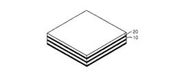
図1は本発明の一実施形態による磁性体シートの製造方法を概略的に示したフローチャートであり、図2は本発明の一実施形態による磁性体シートの概略的な斜視図である。 FIG. 1 is a flowchart schematically showing a method of manufacturing a magnetic sheet according to an embodiment of the present invention, and FIG. 2 is a schematic perspective view of the magnetic sheet according to an embodiment of the present invention.
図1及び図2を参照すると、本発明の一実施形態による磁性体シートの製造方法は、絶縁層10を製造する段階と、上記絶縁層10の上部に金属層20を形成して積層体を製造する段階と、2以上の上記積層体を積層した後に圧着する段階と、を含むことができる。
Referring to FIGS. 1 and 2, a method for manufacturing a magnetic sheet according to an embodiment of the present invention includes a step of manufacturing an
磁性体シートの透磁率を高くするためには、従来用いられていたフレーク(flake)形粉末の体積分率と縦横比(aspect ratio)を増加させなければならない。 In order to increase the magnetic permeability of the magnetic sheet, it is necessary to increase the volume fraction and aspect ratio of the flake-type powder that has been conventionally used.
上記縦横比が無限大になる場合、フレーク形粉末は無限に広い薄膜の形態となる。 When the aspect ratio is infinite, the flake powder is in the form of an infinitely thin film.
したがって、本発明の一実施形態による磁性体シートは、非常に薄い金属層20で形成されることができる。
Therefore, the magnetic sheet according to the embodiment of the present invention can be formed of a very
具体的には、金属層20の厚さは0.1μm〜3.0μmであることができる。
Specifically, the thickness of the
金属層20の厚さが0.1μm未満の場合は、実質的に磁性体シートとして作動することができず、金属層20の厚さが3.0μmを超える場合は、その厚さが厚くなりすぎて商用性が落ちる。
When the thickness of the
したがって、金属層20の厚さが0.1μm〜3.0μmの場合に、通信距離の増大と無接点電力伝送装置の効率増加等の効果が得られ、商用性も確保することができる。
Therefore, when the thickness of the
本発明の一実施形態による製造方法において、上記積層体を製造する段階は3Dプリンティング法で行われることができるが、これに制限されるものではない。 In the manufacturing method according to an embodiment of the present invention, the step of manufacturing the laminate may be performed by a 3D printing method, but is not limited thereto.
3Dプリンティングとは、既存のリソグラフィー技術を用いずにスクリーン印刷のみで微細な金属膜又は金属パターンをプラスチックやポリマー基材に形成することを意味する。 3D printing means forming a fine metal film or metal pattern on a plastic or polymer substrate only by screen printing without using an existing lithography technique.
これは、金、銀、純鉄、フェライトのような金属又は合金のナノ粒子ペーストをインクジェット技術で印刷することにより可能となる。 This is made possible by printing a nanoparticle paste of a metal or alloy such as gold, silver, pure iron, or ferrite using an inkjet technique.
上記金属ナノ粒子ペーストの主成分としては、平均粒径が数〜数十ナノメートル(nm)であり、粒径の分布の狭い金属ナノ粒子が用いられる。 As the main component of the metal nanoparticle paste, metal nanoparticles having an average particle size of several to several tens of nanometers (nm) and a narrow particle size distribution are used.
上記ペーストは、金属の含量と粘度等を調整して製作される。 The paste is manufactured by adjusting the metal content and viscosity.
3Dプリンティング法で金属ナノ粒子ペーストを塗布し焼成して得られる導電膜は、バルク(bulk)な金属の比抵抗に近い性質を有することができる。 A conductive film obtained by applying and baking a metal nanoparticle paste by a 3D printing method may have properties close to the specific resistance of a bulk metal.
したがって、本発明の金属層20は、金属ナノ粒子ペーストを用いて3Dプリンティング法で形成されることにより、非常に薄い厚さと、バルクな金属層と類似した性質を有することができる。
Therefore, the
また、上記金属層20の縦横比(aspect ratio)を増加させ且つバルクな金属層の性質を維持することができるため、上記金属層20の透磁率が増加する。
In addition, since the aspect ratio of the
上記絶縁層10は、上記金属層20の間に位置するため、積層体においてそれぞれの金属層20が互いに絶縁されるようにすることができる。
Since the insulating
上記絶縁層10の厚さは、絶縁可能な厚さであって最大限薄い厚さであることが良い。
The thickness of the insulating
上記絶縁層10の厚さを薄く形成することにより、工程費用を減少させることができる。
The process cost can be reduced by forming the insulating
上記絶縁層10の材料は、ポリマー又はセラミックであることができるが、これに制限されるものではない。
The material of the insulating
上記磁性体シートが無接点電力伝送装置から熱を放出する経路を提供できるよう、上記絶縁層10の材料は熱伝導度に優れた材料であることが良い。
The material of the insulating
上記絶縁層10の材料は、優れた熱伝導度及び絶縁性を有するエポキシ(epoxy)であることが好ましい。
The material of the insulating
上記絶縁層10がセラミックの場合は、上記金属層との接着性が落ちる可能性がある。
When the insulating
よって、上記絶縁層10と上記金属層20は、接着層(図示せず)を挿入して付着されることができる。
Therefore, the insulating
上記接着層の材料は、ポリマー、又は優れた熱伝導度及び絶縁性を有するエポキシ(epoxy)であることができる。 The material of the adhesive layer may be a polymer or an epoxy having excellent thermal conductivity and insulation.
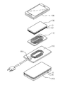
図3は、本発明の他の実施形態による無接点電力伝送装置の概略的な分解斜視図である。 FIG. 3 is a schematic exploded perspective view of a non-contact power transmission apparatus according to another embodiment of the present invention.
図3を参照すると、本発明の他の実施形態による無接点電力伝送装置は、コイル部110、210と、上記コイル部110、210の一面に形成され、複数の金属層20及び上記複数の金属層20の間に位置する絶縁層10を含む磁性体シート120、220と、を含むことができる。
Referring to FIG. 3, the contactless power transmission apparatus according to another embodiment of the present invention includes
上記無接点電力伝送装置のコイル部110、210は基板の上部に配線パターン状に形成され、1つのコイルが連結されるか又は多数のコイルが並列に連結されて1つのコイルパターンを形成することができる。
The
上記コイル部110、210は、巻線形又は柔軟性フィルム形に製作されることができるが、これに制限されるものではない。
The
上記コイル部110、210は、電源入力部230から入力される電源を誘導磁場を用いて送信したり誘導磁場を受信して電源を出力するようにすることにより、無接点電力送信を可能にする。
The
上述したように、無接点電力伝送装置は、一定距離離隔した状態で誘導磁場を送受信して電子機器130等を充電することができる。
As described above, the contactless power transmission device can charge the
無接点電力伝送の場合、ファラデーの法則(Faraday's law)により時間当たりに変化する磁束の流れの変化量によって充電効率が決まる。 In the case of contactless power transmission, the charging efficiency is determined by the amount of change in the flow of magnetic flux that changes per time according to Faraday's law.
この際、透磁率を高くするために、透磁率の高い磁性体シートを用いることができる。 At this time, in order to increase the magnetic permeability, a magnetic material sheet having a high magnetic permeability can be used.
磁性体シート120、220は、無接点電力伝送装置の充電効率を高くする機能をすることができる。
The
磁性体シート120、220は、商用性を確保するために最小限の厚さ内で誘導磁場を所望の方向に集束させて電子機器130の回路、バッテリー等への誘導磁場の影響を最小化することができる。
The
また、金属層20は、うず損失(eddy loss)によって発生する熱を放出する経路を提供することができる。
In addition, the
以上、本発明の実施形態について詳細に説明したが、本発明の権利範囲はこれに限定されず、特許請求の範囲に記載された本発明の技術的思想から外れない範囲内で多様な修正及び変形が可能であるということは、当技術分野の通常の知識を有する者には明らかである。 Although the embodiment of the present invention has been described in detail above, the scope of the right of the present invention is not limited to this, and various modifications and modifications can be made without departing from the technical idea of the present invention described in the claims. It will be apparent to those skilled in the art that variations are possible.
10 絶縁層
20 金属層
110、210 コイル部
120、220 磁性体シート
130 電子機器
230 電源入力部
DESCRIPTION OF
Claims (18)
前記絶縁層の上部に金属層を形成して積層体を製造する段階と、
2以上の前記積層体を積層した後に圧着する段階と、
を含む、磁性体シートの製造方法。 Producing an insulating layer;
Forming a metal layer on the insulating layer to produce a laminate;
Crimping after laminating two or more of the laminates;
A method for producing a magnetic sheet, comprising:
前記複数の金属層の間に位置する絶縁層と、
を含む、磁性体シート。 Multiple metal layers;
An insulating layer located between the plurality of metal layers;
A magnetic sheet.
前記コイル部の一面に形成され、複数の金属層及び前記複数の金属層の間に位置する絶縁層で構成される磁性体シートと、
を含む、無接点電力伝送装置。 A coil section;
A magnetic sheet formed on one surface of the coil portion and configured by a plurality of metal layers and an insulating layer located between the plurality of metal layers;
A non-contact power transmission device.
Applications Claiming Priority (2)
| Application Number | Priority Date | Filing Date | Title |
|---|---|---|---|
| KR1020120150309A KR101444552B1 (en) | 2012-12-21 | 2012-12-21 | Magnetic sheet, method for manufacturing the same, and contactless power transmission device including the same |
| KR10-2012-0150309 | 2012-12-21 |
Publications (1)
| Publication Number | Publication Date |
|---|---|
| JP2014123718A true JP2014123718A (en) | 2014-07-03 |
Family
ID=50973981
Family Applications (1)
| Application Number | Title | Priority Date | Filing Date |
|---|---|---|---|
| JP2013238829A Pending JP2014123718A (en) | 2012-12-21 | 2013-11-19 | Magnetic sheet, method for manufacturing magnetic sheet, and contactless power charger including magnetic sheet |
Country Status (3)
| Country | Link |
|---|---|
| US (1) | US20140176290A1 (en) |
| JP (1) | JP2014123718A (en) |
| KR (1) | KR101444552B1 (en) |
Cited By (1)
| Publication number | Priority date | Publication date | Assignee | Title |
|---|---|---|---|---|
| JP2022537260A (en) * | 2019-06-17 | 2022-08-25 | インターナショナル・ビジネス・マシーンズ・コーポレーション | Particle-based anisotropic composites for magnetic cores |
Families Citing this family (5)
| Publication number | Priority date | Publication date | Assignee | Title |
|---|---|---|---|---|
| CN105448489A (en) * | 2014-08-11 | 2016-03-30 | 介面光电股份有限公司 | Thin film coil, thin film coil assembly and charging device |
| CN107690742B (en) * | 2015-05-29 | 2021-01-12 | 高通股份有限公司 | Wireless power transfer using direct field penetrating metal object |
| DE102018118551A1 (en) * | 2018-07-31 | 2020-02-06 | Tdk Electronics Ag | Method for producing an inductive component and inductive component |
| US20220394854A1 (en) * | 2021-06-04 | 2022-12-08 | Electronics And Telecommunications Research Institute | Method and system for making coil for wireless charging |
| KR102742739B1 (en) * | 2021-06-04 | 2024-12-16 | 한국전자통신연구원 | Method and system for making coil for wireless charging |
Citations (3)
| Publication number | Priority date | Publication date | Assignee | Title |
|---|---|---|---|---|
| JP2005116764A (en) * | 2003-10-07 | 2005-04-28 | Tdk Corp | Method for manufacturing multilayer soft magnetic member and soft magnetic sheet |
| WO2006059771A1 (en) * | 2004-12-03 | 2006-06-08 | Nitta Corporation | Electromagnetic interference inhibitor, antenna device and electronic communication apparatus |
| JP2011134959A (en) * | 2009-12-25 | 2011-07-07 | Hitachi Metals Ltd | Magnetic sheet |
Family Cites Families (13)
| Publication number | Priority date | Publication date | Assignee | Title |
|---|---|---|---|---|
| DE4117878C2 (en) * | 1990-05-31 | 1996-09-26 | Toshiba Kawasaki Kk | Planar magnetic element |
| WO1998044517A1 (en) * | 1997-04-03 | 1998-10-08 | Kawasaki Steel Corporation | Ultra-low iron loss unidirectional silicon steel sheet |
| JP2000269059A (en) * | 1999-03-16 | 2000-09-29 | Nippon Telegr & Teleph Corp <Ntt> | Magnetic component and method of manufacturing the same |
| US6124650A (en) * | 1999-10-15 | 2000-09-26 | Lucent Technologies Inc. | Non-volatile MEMS micro-relays using magnetic actuators |
| EP1426982A4 (en) * | 2001-08-31 | 2004-11-17 | Tdk Corp | Laminated soft magnetic member, soft magnetic sheet and production method for laminated soft magnetic member |
| JP4738923B2 (en) * | 2005-07-15 | 2011-08-03 | 東光株式会社 | Manufacturing method of multilayer inductor for high current |
| JP4281837B2 (en) * | 2007-02-20 | 2009-06-17 | セイコーエプソン株式会社 | COIL UNIT, MANUFACTURING METHOD THEREOF, AND ELECTRONIC DEVICE |
| JP2008294385A (en) * | 2007-04-24 | 2008-12-04 | Panasonic Electric Works Co Ltd | Non-contact power transmission device and method for manufacturing coil block for receiving power |
| US8922160B2 (en) * | 2007-08-21 | 2014-12-30 | Kabushiki Kaisha Toshiba | Non-contact type power receiving apparatus, electronic equipment and charging system using the power receiving apparatus |
| JP4572953B2 (en) * | 2008-05-14 | 2010-11-04 | セイコーエプソン株式会社 | Coil unit and electronic device using the same |
| US20120274148A1 (en) * | 2011-04-27 | 2012-11-01 | Samsung Electro-Mechanics Co., Ltd. | Contactless power transmission device and electronic device having the same |
| KR101179398B1 (en) * | 2011-04-27 | 2012-09-04 | 삼성전기주식회사 | Contactless power transmission device and electronic device having the same |
| JP2020005214A (en) * | 2018-06-29 | 2020-01-09 | キヤノン株式会社 | Imaging device |
-
2012
- 2012-12-21 KR KR1020120150309A patent/KR101444552B1/en not_active Expired - Fee Related
-
2013
- 2013-11-19 JP JP2013238829A patent/JP2014123718A/en active Pending
- 2013-12-20 US US14/137,794 patent/US20140176290A1/en not_active Abandoned
Patent Citations (3)
| Publication number | Priority date | Publication date | Assignee | Title |
|---|---|---|---|---|
| JP2005116764A (en) * | 2003-10-07 | 2005-04-28 | Tdk Corp | Method for manufacturing multilayer soft magnetic member and soft magnetic sheet |
| WO2006059771A1 (en) * | 2004-12-03 | 2006-06-08 | Nitta Corporation | Electromagnetic interference inhibitor, antenna device and electronic communication apparatus |
| JP2011134959A (en) * | 2009-12-25 | 2011-07-07 | Hitachi Metals Ltd | Magnetic sheet |
Cited By (2)
| Publication number | Priority date | Publication date | Assignee | Title |
|---|---|---|---|---|
| JP2022537260A (en) * | 2019-06-17 | 2022-08-25 | インターナショナル・ビジネス・マシーンズ・コーポレーション | Particle-based anisotropic composites for magnetic cores |
| JP7427034B2 (en) | 2019-06-17 | 2024-02-02 | インターナショナル・ビジネス・マシーンズ・コーポレーション | Particle-based anisotropic composites for magnetic cores |
Also Published As
| Publication number | Publication date |
|---|---|
| KR101444552B1 (en) | 2014-10-30 |
| US20140176290A1 (en) | 2014-06-26 |
| KR20140081023A (en) | 2014-07-01 |
Similar Documents
| Publication | Publication Date | Title |
|---|---|---|
| JP5965148B2 (en) | Power receiving module for mobile terminal using wireless power transmission and rechargeable battery for mobile terminal equipped with power receiving module for mobile terminal | |
| US10566824B2 (en) | Wireless power transfer module for vehicles | |
| CN104823324B (en) | Coil module | |
| KR101452093B1 (en) | Thin film coil, shield part including the same, and contactless power transmission device having the shield part | |
| US20160035477A1 (en) | Thin-film coil component and charging apparatus and method for manufacturing the component | |
| CN102792401B (en) | Wireless power transmission magnetic cell and power supply device | |
| US9960630B2 (en) | Wireless power charging device | |
| JP2014123718A (en) | Magnetic sheet, method for manufacturing magnetic sheet, and contactless power charger including magnetic sheet | |
| US20140176282A1 (en) | Electromagnetic induction module for wireless charging element and method of manufacturing the same | |
| US20190214180A1 (en) | Magnetic sheet and wireless power receiving device comprising same | |
| JP2011187559A (en) | Contactless power transmission film | |
| JPWO2013172349A1 (en) | Antenna sheet for non-contact charging device and charging device using the sheet | |
| CN106170196B (en) | Sheet for shielding electromagnetic wave and wireless charging device | |
| JP2014183469A (en) | Antenna device and electronic equipment | |
| JP2012204440A (en) | Magnetic element for wireless power transmission and manufacturing method of the same | |
| WO2014148312A1 (en) | Antenna apparatus and electronic device | |
| JPWO2018100975A1 (en) | Composite coil module and magnetic sheet | |
| WO2019111848A1 (en) | Coil module | |
| KR102034231B1 (en) | Receiving antennas and wireless power receiving apparatus comprising the same | |
| CN106464023A (en) | Thin high-efficiency wireless charging coil and wireless charging system thereof | |
| KR102315813B1 (en) | Heat dissipation member for reception device module of wireless power charger, Reception device module of wireless power charger containing the same and Reception device of wireless power charger containing the same | |
| US11694829B2 (en) | Magnetic sheet and wireless power module comprising same | |
| US20140176281A1 (en) | Electromagnetic induction module for wireless charging element and method of manufacturing the same | |
| KR20160043293A (en) | Coil type unit for wireless power transmission and manufacturing method of coil type unit for wireless power transmission | |
| CN105742004B (en) | Inductor and its manufacturing method |
Legal Events
| Date | Code | Title | Description |
|---|---|---|---|
| A977 | Report on retrieval |
Free format text: JAPANESE INTERMEDIATE CODE: A971007 Effective date: 20141027 |
|
| A131 | Notification of reasons for refusal |
Free format text: JAPANESE INTERMEDIATE CODE: A131 Effective date: 20141104 |
|
| A601 | Written request for extension of time |
Free format text: JAPANESE INTERMEDIATE CODE: A601 Effective date: 20150204 |
|
| A521 | Request for written amendment filed |
Free format text: JAPANESE INTERMEDIATE CODE: A523 Effective date: 20150304 |
|
| A02 | Decision of refusal |
Free format text: JAPANESE INTERMEDIATE CODE: A02 Effective date: 20151013 |