JP2014027259A - Led package and display apparatus having the same - Google Patents
Led package and display apparatus having the same Download PDFInfo
- Publication number
- JP2014027259A JP2014027259A JP2013098758A JP2013098758A JP2014027259A JP 2014027259 A JP2014027259 A JP 2014027259A JP 2013098758 A JP2013098758 A JP 2013098758A JP 2013098758 A JP2013098758 A JP 2013098758A JP 2014027259 A JP2014027259 A JP 2014027259A
- Authority
- JP
- Japan
- Prior art keywords
- light
- core
- phosphor
- led package
- shell
- Prior art date
- Legal status (The legal status is an assumption and is not a legal conclusion. Google has not performed a legal analysis and makes no representation as to the accuracy of the status listed.)
- Pending
Links
Images


Classifications
-
- H—ELECTRICITY
- H01—ELECTRIC ELEMENTS
- H01L—SEMICONDUCTOR DEVICES NOT COVERED BY CLASS H10
- H01L33/00—Semiconductor devices with at least one potential-jump barrier or surface barrier specially adapted for light emission; Processes or apparatus specially adapted for the manufacture or treatment thereof or of parts thereof; Details thereof
- H01L33/48—Semiconductor devices with at least one potential-jump barrier or surface barrier specially adapted for light emission; Processes or apparatus specially adapted for the manufacture or treatment thereof or of parts thereof; Details thereof characterised by the semiconductor body packages
- H01L33/50—Wavelength conversion elements
- H01L33/501—Wavelength conversion elements characterised by the materials, e.g. binder
- H01L33/502—Wavelength conversion materials
-
- H—ELECTRICITY
- H01—ELECTRIC ELEMENTS
- H01L—SEMICONDUCTOR DEVICES NOT COVERED BY CLASS H10
- H01L33/00—Semiconductor devices with at least one potential-jump barrier or surface barrier specially adapted for light emission; Processes or apparatus specially adapted for the manufacture or treatment thereof or of parts thereof; Details thereof
- H01L33/48—Semiconductor devices with at least one potential-jump barrier or surface barrier specially adapted for light emission; Processes or apparatus specially adapted for the manufacture or treatment thereof or of parts thereof; Details thereof characterised by the semiconductor body packages
- H01L33/50—Wavelength conversion elements
-
- H—ELECTRICITY
- H01—ELECTRIC ELEMENTS
- H01L—SEMICONDUCTOR DEVICES NOT COVERED BY CLASS H10
- H01L33/00—Semiconductor devices with at least one potential-jump barrier or surface barrier specially adapted for light emission; Processes or apparatus specially adapted for the manufacture or treatment thereof or of parts thereof; Details thereof
- H01L33/48—Semiconductor devices with at least one potential-jump barrier or surface barrier specially adapted for light emission; Processes or apparatus specially adapted for the manufacture or treatment thereof or of parts thereof; Details thereof characterised by the semiconductor body packages
-
- H—ELECTRICITY
- H01—ELECTRIC ELEMENTS
- H01L—SEMICONDUCTOR DEVICES NOT COVERED BY CLASS H10
- H01L33/00—Semiconductor devices with at least one potential-jump barrier or surface barrier specially adapted for light emission; Processes or apparatus specially adapted for the manufacture or treatment thereof or of parts thereof; Details thereof
- H01L33/02—Semiconductor devices with at least one potential-jump barrier or surface barrier specially adapted for light emission; Processes or apparatus specially adapted for the manufacture or treatment thereof or of parts thereof; Details thereof characterised by the semiconductor bodies
- H01L33/08—Semiconductor devices with at least one potential-jump barrier or surface barrier specially adapted for light emission; Processes or apparatus specially adapted for the manufacture or treatment thereof or of parts thereof; Details thereof characterised by the semiconductor bodies with a plurality of light emitting regions, e.g. laterally discontinuous light emitting layer or photoluminescent region integrated within the semiconductor body
-
- H—ELECTRICITY
- H01—ELECTRIC ELEMENTS
- H01L—SEMICONDUCTOR DEVICES NOT COVERED BY CLASS H10
- H01L2224/00—Indexing scheme for arrangements for connecting or disconnecting semiconductor or solid-state bodies and methods related thereto as covered by H01L24/00
- H01L2224/01—Means for bonding being attached to, or being formed on, the surface to be connected, e.g. chip-to-package, die-attach, "first-level" interconnects; Manufacturing methods related thereto
- H01L2224/42—Wire connectors; Manufacturing methods related thereto
- H01L2224/47—Structure, shape, material or disposition of the wire connectors after the connecting process
- H01L2224/48—Structure, shape, material or disposition of the wire connectors after the connecting process of an individual wire connector
- H01L2224/4805—Shape
- H01L2224/4809—Loop shape
- H01L2224/48091—Arched
-
- H—ELECTRICITY
- H01—ELECTRIC ELEMENTS
- H01L—SEMICONDUCTOR DEVICES NOT COVERED BY CLASS H10
- H01L2224/00—Indexing scheme for arrangements for connecting or disconnecting semiconductor or solid-state bodies and methods related thereto as covered by H01L24/00
- H01L2224/01—Means for bonding being attached to, or being formed on, the surface to be connected, e.g. chip-to-package, die-attach, "first-level" interconnects; Manufacturing methods related thereto
- H01L2224/42—Wire connectors; Manufacturing methods related thereto
- H01L2224/47—Structure, shape, material or disposition of the wire connectors after the connecting process
- H01L2224/48—Structure, shape, material or disposition of the wire connectors after the connecting process of an individual wire connector
- H01L2224/481—Disposition
- H01L2224/48151—Connecting between a semiconductor or solid-state body and an item not being a semiconductor or solid-state body, e.g. chip-to-substrate, chip-to-passive
- H01L2224/48221—Connecting between a semiconductor or solid-state body and an item not being a semiconductor or solid-state body, e.g. chip-to-substrate, chip-to-passive the body and the item being stacked
- H01L2224/48245—Connecting between a semiconductor or solid-state body and an item not being a semiconductor or solid-state body, e.g. chip-to-substrate, chip-to-passive the body and the item being stacked the item being metallic
- H01L2224/48247—Connecting between a semiconductor or solid-state body and an item not being a semiconductor or solid-state body, e.g. chip-to-substrate, chip-to-passive the body and the item being stacked the item being metallic connecting the wire to a bond pad of the item
-
- H—ELECTRICITY
- H01—ELECTRIC ELEMENTS
- H01L—SEMICONDUCTOR DEVICES NOT COVERED BY CLASS H10
- H01L33/00—Semiconductor devices with at least one potential-jump barrier or surface barrier specially adapted for light emission; Processes or apparatus specially adapted for the manufacture or treatment thereof or of parts thereof; Details thereof
- H01L33/48—Semiconductor devices with at least one potential-jump barrier or surface barrier specially adapted for light emission; Processes or apparatus specially adapted for the manufacture or treatment thereof or of parts thereof; Details thereof characterised by the semiconductor body packages
- H01L33/50—Wavelength conversion elements
- H01L33/501—Wavelength conversion elements characterised by the materials, e.g. binder
Abstract
Description
本発明はLEDパッケージ及びこれを有する表示装置に関し、より詳細には蛍光体を利用して発生する光の波長が制御されるLEDパッケージ及びこれを光源として有する表示装置に関する。 The present invention relates to an LED package and a display device having the LED package, and more particularly to an LED package in which the wavelength of light generated using a phosphor is controlled and a display device having the LED package as a light source.
最近、表示装置の光源として発光ダイオードを含むLEDパッケージが適用されている。発光ダイオードは冷陰極蛍光ランプより低電力で駆動が可能であり、高輝度の光を得られる。したがって、LEDパッケージは表示装置の光源だけでなく、一般照明装置にも幅広く使用されている。 Recently, an LED package including a light emitting diode has been applied as a light source of a display device. The light-emitting diode can be driven with lower power than a cold cathode fluorescent lamp, and light with high luminance can be obtained. Therefore, LED packages are widely used not only for light sources of display devices but also for general lighting devices.
一方、互いに異なる色を発光する多数の発光ダイオードを組合してLEDパッケージから発生する光の色相が調節されることがある。しかし、この場合、多数の発光ダイオードを駆動するため、LEDパッケージの駆動回路が複雑になる。そのため、LEDパッケージの小型化を具現するのが容易でない。したがって、LEDパッケージから発生する光の色相を調節するためにLEDパッケージに蛍光体が適用されている。蛍光体は発光ダイオードから発生する光を受信してその波長を変更させる。したがって、LEDパッケージで最終的に出射される光の色相は発光ダイオードから出射される光の色相及び蛍光体から出射される光の色相によって調節され得る。この場合に、蛍光体の発光効率及び信頼性はLEDパッケージの発光に関連する品質に影響を与える。 Meanwhile, the hue of light generated from the LED package may be adjusted by combining a plurality of light emitting diodes that emit different colors. However, in this case, since a large number of light emitting diodes are driven, the driving circuit of the LED package becomes complicated. Therefore, it is not easy to realize downsizing of the LED package. Therefore, a phosphor is applied to the LED package in order to adjust the hue of light generated from the LED package. The phosphor receives light generated from the light emitting diode and changes its wavelength. Therefore, the hue of light finally emitted from the LED package can be adjusted by the hue of light emitted from the light emitting diode and the hue of light emitted from the phosphor. In this case, the luminous efficiency and reliability of the phosphor affect the quality associated with the light emission of the LED package.
本発明の一目的は発光効率及び発光機能の信頼性が向上されたLEDパッケージを提供することにある。 An object of the present invention is to provide an LED package with improved luminous efficiency and reliability of light emitting function.
本発明の他の目的は上述したLEDパッケージを含む表示装置を提供することにある。 Another object of the present invention is to provide a display device including the LED package described above.
上述した本発明の一目的を達成するために、本発明によるLEDパッケージは、第1光を発生する発光ダイオード、前記第1光を吸収して前記第1光と異なる波長を有する第2光を発生する蛍光体、及び前記蛍光体の表面に具備される少なくとも1つのコアシェル粒子を含む。また、前記コアシェル粒子は、前記第1光及び前記第2光の中で少なくとも1つの光成分を受信して表面プラズモン共鳴(surface plasmon resonance)を誘導する金属粒子、及び前記金属粒子の表面にコーティングされる絶縁層を含む。 To achieve the above-described object of the present invention, an LED package according to the present invention includes a light emitting diode that generates first light, and second light that absorbs the first light and has a wavelength different from that of the first light. And a phosphor to be generated and at least one core-shell particle provided on a surface of the phosphor. In addition, the core-shell particles receive at least one light component of the first light and the second light and induce surface plasmon resonance, and the surface of the metal particles is coated. Including an insulating layer.
上述した本発明の他の目的を達成するために、本発明による表示装置は、光を受信して映像を表示する表示パネル及び前記光を発生するLEDパッケージを含む。前記光は前記LEDパッケージから発生する第1光及び第2光を含む。 In order to achieve another object of the present invention, a display device according to the present invention includes a display panel that receives light and displays an image, and an LED package that generates the light. The light includes first light and second light generated from the LED package.
また、前記LEDパッケージは、前記第1光を発生する発光ダイオード、前記第1光を吸収して前記第1光と異なる波長を有する第2光を発生する蛍光体、及び前記蛍光体の表面に具備される少なくとも1つのコアシェル粒子を含む。前記コアシェル粒子は、前記第1光及び前記第2光の中で少なくとも1つの光成分を受信して表面プラズモン共鳴(surface plasmon resonance)を誘導する金属粒子、及び前記金属粒子の表面にコーティングされる絶縁層を含む。 The LED package includes a light emitting diode that generates the first light, a phosphor that absorbs the first light and generates a second light having a wavelength different from that of the first light, and a surface of the phosphor. At least one core-shell particle provided. The core-shell particle is coated on a metal particle that receives at least one light component of the first light and the second light and induces surface plasmon resonance, and a surface of the metal particle. Insulating layer is included.
本発明の一実施形態によれば、前記表示パネルは液晶表示パネルであり得る。 According to an embodiment of the present invention, the display panel may be a liquid crystal display panel.
本発明の他の実施形態によれば、前記表示パネルはエレクトロ・ウェッティング表示パネルであり得る。 According to another embodiment of the present invention, the display panel may be an electrowetting display panel.
本発明によれば、発光効率及び発光機能の信頼性が向上されたLEDパッケージ及び表示装置を提供することができる。 ADVANTAGE OF THE INVENTION According to this invention, the LED package and display apparatus with which the luminous efficiency and the reliability of the light emission function were improved can be provided.
以下、添付した図面を参照して本発明の実施形態を詳細に説明する。上述した本発明の目的、特徴及び効果は図面に関連された実施形態を通じて容易に理解され得る。但し、本発明はここで説明される実施形態に限定されなく、多様な形態に応用されて変形されることもあり得る。むしろ後述される本発明の実施形態は本発明によって開示された技術思想をより明確にし、さらに本発明が属する分野で平均的な知識を有する当業者に本発明の技術思想が十分に伝達され得るように提供される。したがって、本発明の範囲が後述される実施形態によって限定されることとして解釈されてはならない。一方、下記の実施形態と図面上に同一の参照番号は同一の構成要素を示す。 Hereinafter, exemplary embodiments of the present invention will be described in detail with reference to the accompanying drawings. The above-described objects, features, and advantages of the present invention can be easily understood through embodiments related to the drawings. However, the present invention is not limited to the embodiments described herein, and may be modified by being applied to various forms. Rather, the embodiments of the present invention described later clarify the technical idea disclosed by the present invention, and the technical idea of the present invention can be sufficiently transmitted to those skilled in the art having average knowledge in the field to which the present invention belongs. As provided. Accordingly, the scope of the present invention should not be construed as limited by the embodiments described below. On the other hand, the same reference numerals in the following embodiments and drawings indicate the same components.
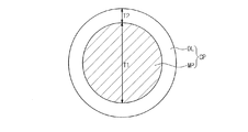
図1は本発明の一実施形態によるLEDパッケージの断面図であり、図2は図1に図示された光学粒子の拡大図であり、図3は図2に図示されたコアシェル粒子の断面図である。 FIG. 1 is a cross-sectional view of an LED package according to an embodiment of the present invention, FIG. 2 is an enlarged view of an optical particle illustrated in FIG. 1, and FIG. 3 is a cross-sectional view of a core-shell particle illustrated in FIG. is there.
図1、図2、及び図3を参照すれば、LEDパッケージ(Light−Emitting Diode Package:100)はモールド10、発光ダイオードLD、保護層20、第1電気端子E1、第2電気端子E2、第1電極線W1、第2電極線W2、及び多数の光学粒子FPを含む。前記多数の光学粒子FPの各々は蛍光体FS及び多数のコアシェル粒子CPを含む。
1, 2, and 3, the LED package (Light-Emitting Diode Package: 100) includes a
前記モールド10はその内部に前記発光ダイオードLDを収納する収納空間を有し、上部が開放された形状を有する。本発明の実施形態では、前記モールド10は絶縁性材料を包含することができる。例えば、前記モールド10はポリフタラミド(Polyphthalamide:PPA)のようなプラスチックを包含することができる。前記発光ダイオードLDは前記モールド10の前記収納空間に収納されて第1光L1を発生し、前記第1光L1は前記発光ダイオードLDの発光面ESを通じて出射される。前記発光ダイオードLDは半導体物質のPN接合を含み、前記発光ダイオードLDは前記PN接合で電子及び正孔の再結合(recombination)にしたがって発生するエネルギーを前記第1光L1として放出させる。本発明の実施形態では、前記半導体物質は砒素化ガリウム(GaAs)、リン化ガリウム(GaP)、及びリン化インジウム(InP)のような酸化物半導体を包含することができる。
The
前記保護層20は絶縁性材料を含み、前記保護層20は前記モールド10の前記収納空間に満たされて前記発光ダイオードLDをカバーする。前記絶縁性材料はシリコン樹脂及びエポキシ樹脂のような光透過度を有する物質を包含でき、この場合に、前記発光ダイオードLDから発生した前記第1光L1は前記保護層20を透過して前記モールド10の外部へ出射されるか、或いは前記多数の光学粒子FP側へ提供され得る。
The
前記第1電気端子E1及び前記第2電気端子E2の各々は導電性材料を含む。前記第1電気端子E1は前記発光ダイオードLDの陽極と電気的に連結され得り、前記第2電気端子E2は前記発光ダイオードLDの陰極と電気的に連結され得る。本発明の実施形態では、前記第1及び第2電気端子E1、E2の各々の一端部は前記モールド10の前記収納空間内に位置し、前記第1及び第2電気端子E1、E2の各々の他端部は前記モールド10の外部へ引き出されることができる。
Each of the first electrical terminal E1 and the second electrical terminal E2 includes a conductive material. The first electrical terminal E1 may be electrically connected to the anode of the light emitting diode LD, and the second electrical terminal E2 may be electrically connected to the cathode of the light emitting diode LD. In an embodiment of the present invention, one end of each of the first and second electrical terminals E1 and E2 is located in the storage space of the
前記第1電極線W1は前記発光ダイオードLDの陽極と前記第1電気端子E1を電気的に連結させ、前記第2電極線W2は前記発光ダイオードLDの陰極と前記第2電気端子E2を電気的に連結させる。したがって、前記第1電気端子E1及び前記第2電気端子E2を外部の電源提供装置の電気端子と電気的に連結させる場合に、前記電源提供装置から提供される電源によって、前記発光ダイオードLDは前記第1光L1を発生できる。 The first electrode line W1 electrically connects the anode of the light emitting diode LD and the first electrical terminal E1, and the second electrode line W2 electrically connects the cathode of the light emitting diode LD and the second electrical terminal E2. Connect to. Therefore, when the first electrical terminal E1 and the second electrical terminal E2 are electrically connected to an electrical terminal of an external power supply device, the light emitting diode LD is caused to be in the form of power by the power supply device. The first light L1 can be generated.
前記多数の光学粒子FPは前記保護層20内部に分散され得る。以下、前記多数の光学粒子FPの中で1つをその例として説明し、残りの光学粒子に対する説明は省略される。
The plurality of optical particles FP may be dispersed inside the
前記光学粒子FPは蛍光体FS及び前記蛍光体FSの表面に具備される多数のコアシェル粒子CPを含む。前記蛍光体FSは前記第1光L1を受信して前記第1光L1と異なる波長を有する第2光L2を発生させる。本発明の実施形態では、前記蛍光体FSの材料は前記第1光L1の色相及び前記LEDパッケージ100から最終出射される出射光の色相にしたがって適切に選択され得る。例えば、前記第1光L1の色相が青色であり、前記出射光が白色とする場合に、前記蛍光体FSはYAG(Yittrium Aluminium Garnet)蛍光物質を包含することができる。この場合に、前記第1光L1の一部は前記YAG蛍光物質に吸収されて前記YAG蛍光物質から黄色光が出射される。したがって、前記YAG蛍光物質の発光に関与しない前記第1光L1の残りと前記黄色光が混合されて前記出射光は白色光になることができる。
The optical particle FP includes a phosphor FS and a number of core-shell particles CP provided on the surface of the phosphor FS. The phosphor FS receives the first light L1 and generates a second light L2 having a wavelength different from that of the first light L1. In an embodiment of the present invention, the material of the phosphor FS may be appropriately selected according to the hue of the first light L1 and the hue of outgoing light finally emitted from the
前記コアシェル粒子CPは前記蛍光体FSの表面に配置される。以下、前記コアシェル粒子CPの中で1つをその例として説明し、残りのコアシェル粒子に対する説明は省略される。 The core-shell particles CP are disposed on the surface of the phosphor FS. Hereinafter, one of the core-shell particles CP will be described as an example, and description of the remaining core-shell particles will be omitted.
前記コアシェル粒子CPは金属粒子MP及び絶縁層DLを含む。前記金属粒子MPは金属材料を含んで粒子形状を有し得り、本発明の実施形態では、前記金属材料は金、白金、銀、パラジウム、カドミウム、コバルト、ルテニウム、銅、インジウム、ニッケル、及び鉄の中でいずれか1つ又はこれらを少なくとも1つ含む合金を包含することができる。 The core shell particle CP includes a metal particle MP and an insulating layer DL. The metal particles MP may have a particle shape including a metal material, and in an embodiment of the present invention, the metal material may be gold, platinum, silver, palladium, cadmium, cobalt, ruthenium, copper, indium, nickel, and Any one of iron or alloys containing at least one of these may be included.
前記絶縁層DLは光透過性を有して前記金属粒子MPの表面をコーティングする。本発明の実施形態では、前記絶縁層DLは窒化物及び酸化物の中の少なくともいずれか1つを包含することができる。例えば、前記酸化物はチタニウム酸化物、シリコン酸化物、マグネシウム酸化物、アルミニウム酸化物、及びイットリウム酸化物の中で少なくともいずれか1つを包含でき、前記窒化物はシリコンナイトライド及びアルミニウムナイトライドの中で少なくともいずれか1つを包含することができる。 The insulating layer DL is light transmissive and coats the surfaces of the metal particles MP. In an embodiment of the present invention, the insulating layer DL may include at least one of nitride and oxide. For example, the oxide may include at least one of titanium oxide, silicon oxide, magnesium oxide, aluminum oxide, and yttrium oxide, and the nitride may be silicon nitride or aluminum nitride. At least one of them can be included.
以下、前記コアシェル粒子CPの機能に対しても図4を参照してより詳細に説明すれば、次の通りである。図4は図3に図示されたコアシェル粒子の表面を拡大して示した図面である。 Hereinafter, the function of the core-shell particle CP will be described in more detail with reference to FIG. FIG. 4 is an enlarged view showing the surface of the core-shell particle shown in FIG.
図4を参照すれば、金属粒子MPの表面に絶縁層DLがコーティングされた場合に、前記金属粒子MP及び前記絶縁層DLの間の界面に電子が集団的に振動する現象、所謂、表面プラズモン(surface plasmon)が発生し、前記表面プラズモンによって電磁気波の一種である表面プラズモン波(surface plamon wave:PP)が生成される。前記表面プラズモン波PPは前記界面に沿って進行する電磁気波の一種であって、空間でランダムな方向に進行する一般的な電磁気波とは異なり、前記表面プラズモン波PPは前記界面と大略的に平行な方向に進行する。 Referring to FIG. 4, when the insulating layer DL is coated on the surface of the metal particle MP, a phenomenon in which electrons collectively vibrate at the interface between the metal particle MP and the insulating layer DL, so-called surface plasmon. (Surface plasmon) is generated, and a surface plasmon wave (PP) which is a kind of electromagnetic wave is generated by the surface plasmon. The surface plasmon wave PP is a kind of electromagnetic wave that travels along the interface, and unlike the general electromagnetic wave that travels in a random direction in space, the surface plasmon wave PP is roughly separated from the interface. Progress in parallel direction.
一方、前記第1光L1及び前記第2光L2の中で少なくともいずれか1つの光成分が前記絶縁層DLを透過して前記金属粒子MP側へ入射する時、前記光成分を入射光ILとして定義し、前記入射光ILが前記金属粒子MPへ入射される角、より詳細には、前記金属粒子MPの表面と垂直である法線PL及び前記入射光ILの間の角を入射角IAとして定義する時、前記入射角IAの特定値に対応して前記入射光ILと前記表面プラズモン波PPの位相が互いに一致することができる。この場合に、前記入射光ILのエネルギーは前記金属粒子MPに吸収され、その結果、前記界面と垂直な方向の電気場分布は指数関数的に増加する。一方で、前記金属粒子MPの内側へ行くほど、前記界面と垂直な方向の電気場分布は急激に減少する現象が発生する。前記現像を所謂表面プラズモン共鳴(surface plasmon resonance)と称し、前記表面プラズモン共鳴が発生する時、前記入射角を共鳴角(surface plasmon resonance angle:RA)と称する。 On the other hand, when at least one of the first light L1 and the second light L2 passes through the insulating layer DL and enters the metal particle MP, the light component is used as incident light IL. And an angle between the incident light IL and the normal light PL perpendicular to the surface of the metal particle MP and the incident light IL is defined as an incident angle IA. When defining, the phases of the incident light IL and the surface plasmon wave PP can coincide with each other corresponding to a specific value of the incident angle IA. In this case, the energy of the incident light IL is absorbed by the metal particles MP, and as a result, the electric field distribution in the direction perpendicular to the interface increases exponentially. On the other hand, a phenomenon occurs in which the electric field distribution in a direction perpendicular to the interface rapidly decreases as the metal particle MP moves inward. The development is referred to as so-called surface plasmon resonance, and when the surface plasmon resonance is generated, the incident angle is referred to as a resonance angle (RA).
したがって、前記表面プラズモン共鳴によって前記金属粒子MPの表面に局部的な電気場(Localized field)が発生し、前記局部的な電気場は前記蛍光体FSの励起された電子が再結合(recombination)される速度を増加させる。したがって、前記電子の再結合速度が増加することによって、前記蛍光体FSが発光できる条件が充足される頻度が増加されるので、結果的に、前記表面プラズモン共鳴によって前記蛍光体FSの発光効率が向上され得る。 Accordingly, a local electric field is generated on the surface of the metal particle MP by the surface plasmon resonance, and the excited electric electrons of the phosphor FS are recombined in the local electric field. Increase speed. Therefore, since the frequency at which the phosphor FS can emit light is increased by increasing the electron recombination rate, the emission efficiency of the phosphor FS is consequently increased by the surface plasmon resonance. Can be improved.
前述したことによれば、前記入射角IAが前記共鳴角RAを満足させる頻度が増加するほど、前記表面プラズモン共鳴によって前記蛍光体FSの発光効率が向上され得る。前記入射角IAが前記共鳴角RAを満足させる頻度を増加させるためには前記第1光L1及び前記第2光L2が散乱されてその進行方向ががランダムであるほど、有利であり得る。しかし、本発明の実施形態では、前記金属粒子MP及び前記絶縁層DLは互に異なる誘電率を有するので、前記入射角IAが臨界角条件を満足する場合に、前記入射光ILが全反射されることができる。したがって、前記全反射によって前記金属粒子MPは前記第1及び第2光L1、L2を散乱させるので、前記第1及び第2光L1、L2の進行方向がランダムになり得、これは各々が前記金属粒子MPを含むコアシェル粒子CPを蛍光体(図3のFS)の表面に配置することによって前記表面プラズモン共鳴によって前記蛍光体FSの発光効率が向上され得ることを意味する。 As described above, the light emission efficiency of the phosphor FS can be improved by the surface plasmon resonance as the frequency at which the incident angle IA satisfies the resonance angle RA increases. In order to increase the frequency at which the incident angle IA satisfies the resonance angle RA, it may be more advantageous that the first light L1 and the second light L2 are scattered and their traveling directions are random. However, in the embodiment of the present invention, since the metal particles MP and the insulating layer DL have different dielectric constants, the incident light IL is totally reflected when the incident angle IA satisfies the critical angle condition. Can. Accordingly, the metal particles MP scatter the first and second lights L1 and L2 due to the total reflection, so that the traveling directions of the first and second lights L1 and L2 may be random. It means that the luminous efficiency of the phosphor FS can be improved by the surface plasmon resonance by arranging the core-shell particles CP containing the metal particles MP on the surface of the phosphor (FS in FIG. 3).
また、前記コアシェル粒子CPは前記蛍光体FSの表面に配置されるので、前記第2光L2の中で前記表面プラズモン共鳴に関与する光成分以外に残りの光成分は前記金属粒子MPを経由するようになる。したがって、前記金属粒子MPによって前記第2光L2が散乱される効果はさらに向上され得るので、前記表面プラズモン共鳴によって前記蛍光体FSの発光効率が向上され得る。 Further, since the core-shell particles CP are disposed on the surface of the phosphor FS, the remaining light components other than the light components involved in the surface plasmon resonance in the second light L2 pass through the metal particles MP. It becomes like this. Therefore, since the effect of scattering the second light L2 by the metal particles MP can be further improved, the light emission efficiency of the phosphor FS can be improved by the surface plasmon resonance.
また、前記コアシェル粒子CPは前記蛍光体FSの表面に配置されるので、温度及び湿度のような外部環境に前記蛍光体が直接的に露出されることを防止することができる。したがって、前記外部環境によって前記蛍光体が劣化されることを低減させることができるので、寿命及び色純度と関連する前記蛍光体の発光機能の信頼性が向上され得る。 Further, since the core-shell particles CP are disposed on the surface of the phosphor FS, it is possible to prevent the phosphor from being directly exposed to an external environment such as temperature and humidity. Accordingly, it is possible to reduce the deterioration of the phosphor due to the external environment, and thus the reliability of the light emitting function of the phosphor related to the lifetime and the color purity can be improved.
図5は本発明の実施形態による絶縁層の厚さに応じた蛍光体の発光強さの相対値を示すグラフである。 FIG. 5 is a graph showing the relative value of the emission intensity of the phosphor according to the thickness of the insulating layer according to the embodiment of the present invention.
図3及び図5を参照すれば、第1グラフG1は本発明の実施形態によるものであって、金属粒子MPが銀を含んでその直径が約3.5ナノメータであり、絶縁層DLがマグネシウムオキサイドを含む場合に、前記第1グラフG1は絶縁層DLの厚さに応じた蛍光体FSの発光強さの相対値を任意単位(arbitrary unit)で示す。 Referring to FIGS. 3 and 5, the first graph G1 is according to an embodiment of the present invention, wherein the metal particle MP includes silver and has a diameter of about 3.5 nanometers, and the insulating layer DL is magnesium. When the oxide is included, the first graph G1 indicates the relative value of the emission intensity of the phosphor FS according to the thickness of the insulating layer DL in an arbitrary unit.
前記第1グラフG1を参照すれば、前記絶縁層DLの厚さが0ナノメータ、即ち、コアシェル粒子CPで前記絶縁層DLが省略された場合に、前記蛍光体FSの発光強さは約1.05である。また、前記絶縁層DLの厚さが1ナノメータ乃至20ナノメータの範囲内では、前記蛍光体FSの発光強さは約1.05から約1.90まで増加し、前記絶縁層DLの厚さT2が20ナノメータ乃至80ナノメータの範囲内では、前記蛍光体FSの発光強さが約1.90から約1.2まで減少する。したがって、前記絶縁層DLの厚さT2が約1ナノメータ乃至約80ナノメータ範囲内において、前記蛍光体FSの発光強さは、前記絶縁層DLの厚さT2が0ナノメータの場合より大きいので、前記絶縁層DLの厚さT2が約1ナノメータ乃至約80ナノメータである範囲内で前記蛍光体FSの発光強さ又は発光効率が向上される効果がある。 Referring to the first graph G1, when the insulating layer DL has a thickness of 0 nanometer, that is, when the insulating layer DL is omitted by the core-shell particles CP, the emission intensity of the phosphor FS is about 1. 05. In addition, when the thickness of the insulating layer DL is within a range of 1 nanometer to 20 nanometers, the emission intensity of the phosphor FS increases from about 1.05 to about 1.90, and the thickness T2 of the insulating layer DL. Is within the range of 20 nanometers to 80 nanometers, the emission intensity of the phosphor FS decreases from about 1.90 to about 1.2. Accordingly, when the thickness T2 of the insulating layer DL is within a range of about 1 nanometer to about 80 nanometers, the emission intensity of the phosphor FS is larger than that when the thickness T2 of the insulating layer DL is 0 nanometer. As long as the thickness T2 of the insulating layer DL is in the range of about 1 nanometer to about 80 nanometer, the luminous intensity or luminous efficiency of the phosphor FS is improved.
また、図5で図示していないが、前記金属粒子MPの直径T1が約1ナノメータ乃至30ナノメータである範囲内である場合に、先に前記第1グラフG1で示された結果と類似に、前記絶縁層DLの厚さT2が約1ナノメータ乃至80ナノメータ範囲内で前記蛍光体FSの発光強さは前記絶縁層DLの厚さT2が0ナノメータである場合より大きい。したがって、本発明の実施形態では、前記金属粒子MPの直径T1は約1ナノメータ乃至30ナノメータであり得る。 Although not shown in FIG. 5, when the diameter T1 of the metal particles MP is within a range of about 1 nanometer to 30 nanometers, similar to the result previously shown in the first graph G1, When the thickness T2 of the insulating layer DL is in the range of about 1 nanometer to 80 nanometers, the emission intensity of the phosphor FS is larger than that when the thickness T2 of the insulating layer DL is 0 nanometer. Accordingly, in an embodiment of the present invention, the diameter T1 of the metal particles MP may be about 1 nanometer to 30 nanometers.
図6は本発明の他の実施形態による光学粒子の断面図である。図6を説明する場合、前述した実施形態で説明された構成要素に対しては図面符号を併記し、前記構成要素に対する重複された説明は省略される。 FIG. 6 is a cross-sectional view of an optical particle according to another embodiment of the present invention. In the case of FIG. 6, the constituent elements described in the above-described embodiment are denoted by the same reference numerals, and redundant description of the constituent elements is omitted.
図6を参照すれば、LEDパッケージ(図1の100)の保護層(図1の20)内に分散された多数の光学粒子の中でその例として1つの光学粒子FP’が図示されている。前記光学粒子FP’は蛍光体FS及び前記蛍光体FSの表面に配置される多数のコアシェル粒子CPを含む。 Referring to FIG. 6, an optical particle FP ′ is illustrated as an example among many optical particles dispersed in the protective layer (20 of FIG. 1) of the LED package (100 of FIG. 1). . The optical particle FP ′ includes a phosphor FS and a number of core-shell particles CP disposed on the surface of the phosphor FS.
図6に図示された実施形態では、図2に図示された実施形態と異なり、前記多数のコアシェル粒子CPは前記蛍光体FSの表面にコーティングされる。この場合に、前記多数のコアシェル粒子CPが前記蛍光体FSの表面にコーティングされるために前記多数のコアシェル粒子CPは前記蛍光体FSの表面に複数の層に積層され得る。 In the embodiment illustrated in FIG. 6, unlike the embodiment illustrated in FIG. 2, the multiple core-shell particles CP are coated on the surface of the phosphor FS. In this case, since the multiple core-shell particles CP are coated on the surface of the phosphor FS, the multiple core-shell particles CP may be stacked on the surface of the phosphor FS in a plurality of layers.
上述したように、前記多数のコアシェル粒子CPが前記蛍光体FSの表面をコーティングする場合に、先に図4を参照して説明したように前記多数のコアシェル粒子CPによって第1光(図4のL1)及び第2光(図4のL2)が散乱される効果がより向上されることができるので、表面プラズモン共鳴によって前記蛍光体FSの発光効率がより向上され得る。また、前記多数のコアシェル粒子CPによって前記蛍光体FSの表面が外部に露出されないので、外部環境によって前記蛍光体FSが劣化されることを防止する効果をより向上され得る。 As described above, when the multiple core-shell particles CP coat the surface of the phosphor FS, as described above with reference to FIG. 4, the first light (FIG. 4) is generated by the multiple core-shell particles CP. Since the effect of scattering L1) and the second light (L2 in FIG. 4) can be further improved, the light emission efficiency of the phosphor FS can be further improved by surface plasmon resonance. In addition, since the surface of the phosphor FS is not exposed to the outside by the large number of core-shell particles CP, the effect of preventing the phosphor FS from being deteriorated by an external environment can be further improved.
図7は本発明の他の実施形態による液晶表示装置の分解斜視図である。 FIG. 7 is an exploded perspective view of a liquid crystal display device according to another embodiment of the present invention.
図7を参照すれば、表示装置600はバックライトアセンブリー500及び表示パネル520を含む。前記バックライトアセンブリー500は光を発生し、前記表示パネル520は前記光を利用して映像を表示する。
Referring to FIG. 7, the
前記バックライトアセンブリー500は多数のLEDパッケージ101、印刷回路基板150、収納容器580、反射板570、導光板550、多数のシート540、モールドフレーム530、及びカバー部材510を含む。
The
前記多数のLEDパッケージ101は前記表示パネル520が映像を表示するのに使用する光を発生する。前記多数のLEDパッケージ101の各々は先に図1を参照して説明されたLEDパッケージ(図1の100)と同一な構造を有するので、前記多数のLEDパッケージ101の構造に対する具体的な説明は省略される。
The plurality of
前記印刷回路基板150は前記多数のLEDパッケージ101と電気的に連結され、これによって、前記印刷回路基板150を通じて前記多数のLEDパッケージ101へ電源を提供することができる。本発明の実施形態では、前記多数のLEDパッケージ101が実装された前記印刷回路基板150は前記導光板550の一側部と対向するように配置され得る。
The printed
前記収納容器580は底部及び前記底部から延長された多数の側壁を具備して、前記バックライトアセンブリー500の構成要素を収納する。本発明の実施形態では、前記多数のLEDパッケージ101から発生した熱を外部へ容易に放出するために前記収納容器580は金属材料を包含することができる。
The receiving
前記導光板550は前記収納容器580に収納されて一側部が前記多数のLEDパッケージ101と対向する。したがって、前記多数のLEDパッケージ101各々の発光面(図1のES)は前記導光板の側部と対向して、前記発光面から出射された光は前記導光板550の側部を通じて入射され得る。また、前記導光板550側へ入射された光は前記導光板550に形成された光ガイドパターン(図示せず)によって外部へ出射されて前記表示パネル520側に提供され得る。
The
前記反射板570はポリエチレンテレフタレート(polyethylene terephthalate:PET)及びアルミニウムのような光を反射する物質を含んで前記収納容器580の底部及び前記導光板550の間に配置される。したがって、前記多数のLEDパッケージ101から発生して前記導光板550側へ入射されなかった光は前記反射板570によって反射された後、前記導光板550へ入射され得る。
The
前記モールドフレーム530は前記収納容器580と結合されて前記導光板550の縁を前記収納容器580に支持する。前記モールドフレーム530の一部分は前記収納容器580の底部と平行な方向に延長されて前記多数のシート540及び前記表示パネル520が前記モールドフレーム530上に安着され得る。
The
前記多数のシート540は前記表示パネル520の上部に配置される。前記多数のシート540は前記導光板550から出射されて前記表示パネル520側へ入射される光の経路を調節する光学シート及び前記表示パネル520の表面を保護する保護シートを包含することができる。本発明の実施形態では、前記多数のシート540は前記表示パネル520の背面を保護する保護シート541、正面での輝度を向上させるプリズムシート543、及び光を拡散させる拡散シート545を包含することができる。
The
前記表示パネル520は前記バックライトアセンブリー500から発生した光を受信して映像を表示する。この実施形態では、前記表示パネル520は液晶表示パネルであり得り、この場合に、前記表示パネル520は多数の画素電極を有する第1基板521、共通電極を有する第2基板522、及び前記第1基板521と前記第2基板522との間に介在された液晶層(図示せず)を包含することができる。
The
カバー部材510は前記表示パネル520の表示領域が露出されるようにその一部が開口され、前記表示パネル520の枠をカバーして前記収納容器580に結合される。前記カバー部材510が前記収納容器580に締結されることによって、前記収納容器580の内部に前記バックライトアセンブリー500の構成要素が安定的に収納され得る。
The
図8は本発明のその他の実施形態による表示装置の断面図である。一方、表示装置601は先に図7を参照して説明されたバックライトアセンブリー500を包含するので、図8を説明する場合において、前記バックライトアセンブリー500に対する具体的な説明は省略される。
FIG. 8 is a cross-sectional view of a display device according to another embodiment of the present invention. On the other hand, since the
図8を参照すれば、表示装置601はバックライトアセンブリー500及び表示パネル521を含む。この実施形態では、前記表示パネル521はエレクトロ・ウェッティング表示パネルであって、前記表示パネル521は前記バックライトアセンブリー500から提供される光LTを利用して映像を表示する。前記表示パネル521の構造に対してより詳細に説明すれば次の通りである。
Referring to FIG. 8, the
前記表示パネル521は第1基板S1、第2基板S2、多数の隔壁WL、エレクトロ・ウェッティング層FL、第1電極ET1、第2電極ET2、疏水性膜HL及び多数のカラーフィルターCFを含む。前記第1基板S1及び前記第2基板S2は互に対向するように配置され、前記第1基板S1及び前記第2基板S2はガラスのような光透過度を有する絶縁物を包含することができる。前記多数の隔壁WLは前記第1基板S1上に配置されて多数の画素領域を定義する。この実施形態において、前記多数の画素領域は前記多数のカラーフィルターCFが配置される領域と一対一対応することができる。
The
本発明の実施形態では、前記多数のカラーフィルターCFは前記第2基板S2上に配置され、前記多数のカラーフィルターCFは赤色フィルターRF、緑色フィルターGF、及び青色フィルターBFを包含することができる。前記多数のカラーフィルターCFは前記バックライトアセンブリー500から発生して前記エレクトロ・ウェッティング層FLを透過した光LTをカラー光にフィルタリングする。
In an embodiment of the present invention, the multiple color filters CF may be disposed on the second substrate S2, and the multiple color filters CF may include a red filter RF, a green filter GF, and a blue filter BF. The plurality of color filters CF filters the light LT generated from the
前記第1電極ET1は前記第1基板S1上に配置され、前記第2電極ET2は前記第2基板S2上に配置されて前記第1電極ET1と対向する。これによって、前記第1電極ET1及び前記第2電極ET2の間に電界が形成され、これによって、前記エレクトロ・ウェッティング層FL内で第1流体F1及び第2流体F2の流動を制御することができる。 The first electrode ET1 is disposed on the first substrate S1, and the second electrode ET2 is disposed on the second substrate S2 and faces the first electrode ET1. Accordingly, an electric field is formed between the first electrode ET1 and the second electrode ET2, thereby controlling the flow of the first fluid F1 and the second fluid F2 in the electrowetting layer FL. it can.
前記疏水性膜HLは前記第1電極ET1をカバーして前記エレクトロ・ウェッティング層FLと接する。これによって、前記疏水性膜HLによって前記エレクトロ・ウェッティング層FL内の疏水性を有する流体と前記疏水性膜HLとの間に湿潤性が向上され得る。 The hydrophobic film HL covers the first electrode ET1 and is in contact with the electrowetting layer FL. Thereby, wettability can be improved between the hydrophobic film HL and the fluid having hydrophobicity in the electrowetting layer FL by the hydrophobic film HL.
前記エレクトロ・ウェッティング層FLは互いに混じらない第1流体F1及び第2流体F2を含む。本発明の実施形態では、前記第1流体F1は電気的に非伝導性であるブラックオイルであり、例えば、ヘキサデカン(hexadecane)のようなアルカン及びシリコンオイルのようなオイルであり得る。また、前記第2流体FL2は電気伝導性又は極性を有し得り、透明であることができる。例えば、前記第2流体FL2は水とエチルアルコール混合物に塩化カリウムが溶解された溶液又は水に塩化カリウムが溶解された溶液であり得る。 The electrowetting layer FL includes a first fluid F1 and a second fluid F2 that are not mixed with each other. In an embodiment of the present invention, the first fluid F1 is a black oil that is electrically non-conductive, for example, an alkane such as hexadecane and an oil such as silicone oil. Also, the second fluid FL2 may have electrical conductivity or polarity and may be transparent. For example, the second fluid FL2 may be a solution in which potassium chloride is dissolved in a mixture of water and ethyl alcohol, or a solution in which potassium chloride is dissolved in water.
したがって、前記第1電極ET1及び前記第2電極ET2の間に形成された電界によって前記第2流体F2及び前記第1電極ET1の間に引力が発生すれば、前記第2流体F2は前記エレクトロ・ウェッティング層FL内で前記第1電極ET1に隣接するように移動する。その結果、前記第1流体F1は前記第2流体F2によって、前記画素領域各々の縁側へ押し寄せることができる。上述した前記エレクトロ・ウェッティング層FL内で前記第1流体F1及び前記第2流体F2の移動にしたがって、前記バックライトアセンブリー500から発生して前記エレクトロ・ウェッティング層FLを透過する前記光LTは前記多数のカラーフィルターCFによってカラー光にフィルタリングされ、これによって、前記カラー光を利用して前記表示パネル521に映像が表示され得る。
Therefore, if an attractive force is generated between the second fluid F2 and the first electrode ET1 by an electric field formed between the first electrode ET1 and the second electrode ET2, the second fluid F2 is electro- It moves so as to be adjacent to the first electrode ET1 in the wetting layer FL. As a result, the first fluid F1 can be pushed toward the edge of each pixel region by the second fluid F2. The light LT generated from the
上述した本発明の実施形態によれば、蛍光体の表面にコアシェル粒子が配置されるか、或いはコーティングされるので、コアシェル粒子各々の金属粒子によって表面プラズモン共鳴が誘導され、前記表面プラズモン共鳴によって発生する局部的電気場によって前記蛍光体の発光効率が向上され得る。 According to the embodiment of the present invention described above, since the core-shell particles are disposed or coated on the surface of the phosphor, surface plasmon resonance is induced by the metal particles of each of the core-shell particles, and is generated by the surface plasmon resonance. The luminous efficiency of the phosphor can be improved by the local electric field.
また、本発明の実施形態によれば、蛍光体の表面にコアシェル粒子が配置されるか、或いはコーティングされるので、コアシェル粒子各々の金属粒子によって発光ダイオード及び蛍光体から発生する光が散乱され得る。したがって、前記散乱された光が前記金属粒子に入射する時の入射角が表面プラズモン共鳴を発生させる共鳴角を充足させる頻度数が増加し、これによって前記表面プラズモン共鳴がより活性化されて前記蛍光体の発光効率がより向上され得る。 In addition, according to the embodiment of the present invention, since the core-shell particles are disposed or coated on the surface of the phosphor, the light generated from the light emitting diode and the phosphor can be scattered by the metal particles of each of the core-shell particles. . Therefore, the frequency at which the incident angle when the scattered light is incident on the metal particle satisfies the resonance angle for generating surface plasmon resonance, thereby increasing the frequency of the surface plasmon resonance and the fluorescence. The luminous efficiency of the body can be further improved.
また、本発明の実施形態によれば、蛍光体の表面にコアシェル粒子が配置されるか、或いはコーティングされるので、温度及び濕度のような外部環境に蛍光体が直接的に露出されることを防止でき、これによって蛍光体が劣化されることを低減させることができる。したがって、寿命及び色純度に関連された蛍光体の発光機能の信頼性が向上され得る。 In addition, according to the embodiment of the present invention, since the core-shell particles are disposed or coated on the surface of the phosphor, the phosphor is directly exposed to an external environment such as temperature and temperature. This can prevent the phosphor from being deteriorated. Therefore, the reliability of the light emitting function of the phosphor related to the lifetime and the color purity can be improved.
以上では本発明の望ましい実施形態を参照して説明したが、該当技術分野の熟練された当業者又は該当技術分野に通常の知識を有する者であれば、後述される特許請求の範囲に記載された本発明のマッピング及び技術領域から逸脱しない範囲内で本発明を多様に修正及び変形できることは理解できる。 Although the present invention has been described with reference to the preferred embodiments of the present invention, those skilled in the relevant technical field or those who have ordinary knowledge in the relevant technical field will be described in the claims described below. It will be understood that the present invention can be variously modified and varied without departing from the mapping and technical field of the present invention.
FP・・・光学粒子
LD・・・発光ダイオード
CP・・・コアシェル粒子
FS・・・蛍光体
DL・・・絶縁層
MP・・・金属粒子
RA・・・共鳴角
IA・・・入射角
IL・・・入射光
100・・・LEDパッケージ
FP ... Optical particle LD ... Light emitting diode CP ... Core shell particle FS ... Phosphor DL ... Insulating layer MP ... Metal particle RA ... Resonance angle IA ... Incident angle IL. ..
Claims (10)
前記第1光を吸収して前記第1光と異なる波長を有する第2光を発生する蛍光体と、
前記蛍光体の表面に具備される少なくとも1つのコアシェル粒子と、を含み、
前記コアシェル粒子は、
前記第1光及び前記第2光の中で少なくとも1つの光成分を受信して表面プラズモン共鳴(surface plasmon resonance)を誘導する金属粒子と、
前記金属粒子の表面にコーティングされる絶縁層と、を含み、
前記コアシェル粒子は前記蛍光体の前記表面に多数に提供され、前記蛍光体の前記表面は前記多数のコアシェル粒子によってカバーされることを特徴とするLEDパッケージ。 A light emitting diode generating first light;
A phosphor that absorbs the first light and generates second light having a wavelength different from that of the first light;
And at least one core-shell particle provided on the surface of the phosphor,
The core-shell particles are
Metal particles that receive at least one light component of the first light and the second light to induce surface plasmon resonance;
An insulating layer coated on the surface of the metal particles,
The LED package according to claim 1, wherein a plurality of the core-shell particles are provided on the surface of the phosphor, and the surface of the phosphor is covered with the plurality of core-shell particles.
前記光を発生するLEDパッケージと、を含み、
前記光は前記LEDパッケージから発生する第1光及び第2光を含み、
前記LEDパッケージは、
前記第1光を発生する発光ダイオードと、
前記第1光を吸収して前記第1光と異なる波長を有する前記第2光を発生する蛍光体と、
前記蛍光体の表面に具備される少なくとも1つのコアシェル粒子と、を含み、
前記コアシェル粒子は、
前記第1光及び前記第2光の中で少なくとも1つの光成分を受信して表面プラズモン共鳴(surface plasmon resonance)を誘導する金属粒子と、
前記金属粒子の表面にコーティングされる絶縁層と、を含む表示装置。 A display panel that receives light and displays an image;
An LED package for generating the light,
The light includes first light and second light generated from the LED package;
The LED package is
A light emitting diode for generating the first light;
A phosphor that absorbs the first light and generates the second light having a wavelength different from that of the first light;
And at least one core-shell particle provided on the surface of the phosphor,
The core-shell particles are
Metal particles that receive at least one light component of the first light and the second light to induce surface plasmon resonance;
And an insulating layer coated on the surface of the metal particles.
The metal particles include any one of gold, platinum, silver, palladium, cadmium, cobalt, ruthenium, copper, indium, nickel, and iron, or an alloy including at least one of these. 4. The display device according to 4.
Applications Claiming Priority (2)
| Application Number | Priority Date | Filing Date | Title |
|---|---|---|---|
| KR1020120080628A KR20140015763A (en) | 2012-07-24 | 2012-07-24 | Light-emitting diode package and display apparatus having the same |
| KR10-2012-0080628 | 2012-07-24 |
Publications (2)
| Publication Number | Publication Date |
|---|---|
| JP2014027259A true JP2014027259A (en) | 2014-02-06 |
| JP2014027259A5 JP2014027259A5 (en) | 2016-06-02 |
Family
ID=49994039
Family Applications (1)
| Application Number | Title | Priority Date | Filing Date |
|---|---|---|---|
| JP2013098758A Pending JP2014027259A (en) | 2012-07-24 | 2013-05-08 | Led package and display apparatus having the same |
Country Status (4)
| Country | Link |
|---|---|
| US (1) | US8829550B2 (en) |
| JP (1) | JP2014027259A (en) |
| KR (1) | KR20140015763A (en) |
| CN (1) | CN103579463A (en) |
Cited By (1)
| Publication number | Priority date | Publication date | Assignee | Title |
|---|---|---|---|---|
| JP2017138558A (en) * | 2016-02-05 | 2017-08-10 | 大日本印刷株式会社 | Picture display unit |
Families Citing this family (6)
| Publication number | Priority date | Publication date | Assignee | Title |
|---|---|---|---|---|
| KR20140089641A (en) | 2013-01-03 | 2014-07-16 | 삼성디스플레이 주식회사 | Light-emitting diode package and display apparatus having the same |
| KR101585773B1 (en) * | 2014-06-12 | 2016-01-15 | 주식회사 효성 | Led encapsulant comprisng a rare earth metal oxide particles |
| KR20160007239A (en) * | 2014-07-11 | 2016-01-20 | 한화토탈 주식회사 | Light emitting device comprising anisotropic metal nanoparticles-dielectric core-shell nanostructure |
| USD892113S1 (en) * | 2017-03-20 | 2020-08-04 | Nazar Fedorchuk | Electronic device |
| CN108011013B (en) * | 2017-10-30 | 2020-03-20 | 佛山市国星光电股份有限公司 | Coated fluorescent powder, preparation method thereof, LED device and LED lamp |
| US20200075816A1 (en) * | 2018-08-30 | 2020-03-05 | Oregon State University | Micro-led apparatus with enhanced illumination, and method for forming such |
Citations (5)
| Publication number | Priority date | Publication date | Assignee | Title |
|---|---|---|---|---|
| JP2001288467A (en) * | 2000-04-06 | 2001-10-16 | Toshiba Corp | Oxide composite particle and method of its manufacture, fluorescent material and method of its manufacture, color filter and method of its manufacture, and color display unit |
| JP2007139540A (en) * | 2005-11-17 | 2007-06-07 | Kyoto Univ | Fluorescence enhancing element, fluorescence element and fluorescence method |
| KR20090105114A (en) * | 2008-04-01 | 2009-10-07 | 삼성전기주식회사 | Phosphor for converting wavelength and light emitting device using the same |
| JP2012255060A (en) * | 2011-06-08 | 2012-12-27 | Panasonic Corp | Phosphor material and plasma display panel using the same |
| JP2013209570A (en) * | 2012-03-30 | 2013-10-10 | Toshiba Corp | Fluorescent complex and method of manufacturing fluorescent complex |
Family Cites Families (26)
| Publication number | Priority date | Publication date | Assignee | Title |
|---|---|---|---|---|
| AU2001250882A1 (en) * | 2000-03-20 | 2001-10-03 | Massachusetts Institute Of Technology | Inorganic particle conjugates |
| AU2001268500A1 (en) * | 2000-06-14 | 2001-12-24 | Board Of Regents, The University Of Texas System | Dielectrically-engineered microparticles |
| JP3849606B2 (en) * | 2002-08-06 | 2006-11-22 | 株式会社日立製作所 | Information recording medium, information recording method, and information reproducing method |
| US7491699B2 (en) * | 2002-12-09 | 2009-02-17 | Ramot At Tel Aviv University Ltd. | Peptide nanostructures and methods of generating and using the same |
| KR20060123537A (en) | 2004-01-29 | 2006-12-01 | 이데미쓰 고산 가부시키가이샤 | Metal oxide phosphor microparticle and process for producing the same, utilizing the same, dispersion liquid, fluorescence conversion membrane, method of separating metal oxide phosphor microparticle, fluorescent liquid, fluorescent paste, phosphor and process for producing the same, and fluorescence converter |
| JP2006259032A (en) | 2005-03-16 | 2006-09-28 | Arima Device Kk | Lens driving device |
| WO2007079585A1 (en) | 2006-01-12 | 2007-07-19 | University Of Manitoba | Metal nanoparticle and use thereof for inducing chirality in liquid crystal phases |
| KR100745745B1 (en) | 2006-02-21 | 2007-08-02 | 삼성전기주식회사 | Nano-composite material and the maunfacturing method for the same |
| KR100867382B1 (en) | 2006-09-30 | 2008-11-10 | 최재봉 | Language Learning Material Comprising Diagrams Expressed between Part Images on a Whole Image |
| WO2009032752A2 (en) | 2007-08-28 | 2009-03-12 | University Of Florida Research Foundation, Inc. | Multimodal nanoparticles for non-invasive bio-imaging |
| KR20100085918A (en) | 2007-09-24 | 2010-07-29 | 사비 테크날러지 인코퍼레이티드 | Method and apparatus for tracking and monitoring containers |
| KR100971210B1 (en) | 2007-12-26 | 2010-07-20 | 주식회사 동부하이텍 | Method of forming quantum dot, and forming gate using the same |
| RU2381304C1 (en) | 2008-08-21 | 2010-02-10 | Федеральное государственное унитарное предприятие "Научно-исследовательский институт прикладной акустики" | Method for synthesis of semiconductor quantum dots |
| KR101018111B1 (en) | 2008-10-07 | 2011-02-25 | 삼성엘이디 주식회사 | Quantum dot-matal oxide complex, preparing method of the same and light-emitting device comprising the same |
| DK2449379T3 (en) * | 2009-07-02 | 2017-08-28 | Sloan-Kettering Inst For Cancer Res | FLUORESCING SILICA-BASED NANOPARTICLES |
| WO2011038335A1 (en) * | 2009-09-25 | 2011-03-31 | Immunolight, Llc | Up and down conversion systems for improved solar cell performance or other energy conversion |
| KR101711085B1 (en) * | 2009-10-09 | 2017-03-14 | 삼성전자 주식회사 | Nano complex particle, method of manufacturing the same, and device including the nano complex particle |
| KR20120012642A (en) * | 2010-08-02 | 2012-02-10 | 삼성전기주식회사 | Nanocomposites and light emitting device package comprising the same |
| JP5389080B2 (en) * | 2010-08-27 | 2014-01-15 | 株式会社東芝 | Metal-containing particle aggregate |
| JP5167419B2 (en) * | 2010-10-19 | 2013-03-21 | 積水化学工業株式会社 | Encapsulant for optical semiconductor device and optical semiconductor device using the same |
| CN104485371A (en) * | 2010-12-06 | 2015-04-01 | 日立化成株式会社 | Spherical phosphor, sealing material for wavelength-conversion-type solar batteries, solar battery module, and process for manufacture of those |
| JP5269115B2 (en) * | 2011-02-03 | 2013-08-21 | シャープ株式会社 | LIGHT EMITTING ELEMENT, LIGHT EMITTING DEVICE, VEHICLE HEADLAMP, LIGHTING DEVICE, AND LIGHT EMITTING DEVICE MANUFACTURING METHOD |
| US20120263793A1 (en) * | 2011-04-14 | 2012-10-18 | Franco Vitaliano | Bio-nano-plasmonic elements and platforms |
| JP5784537B2 (en) * | 2012-03-30 | 2015-09-24 | 株式会社東芝 | Radio wave absorber |
| TW201347232A (en) * | 2012-05-08 | 2013-11-16 | Chi Mei Lighting Tech Corp | Light-emitting diode structure and method for manufacturing the same |
| CN104487540B (en) * | 2012-05-22 | 2017-06-20 | 纳米技术有限公司 | Use the raising of the quantum yield of the reagent of high reflection |
-
2012
- 2012-07-24 KR KR1020120080628A patent/KR20140015763A/en not_active Application Discontinuation
-
2013
- 2013-01-15 US US13/742,151 patent/US8829550B2/en active Active
- 2013-04-18 CN CN201310135226.8A patent/CN103579463A/en active Pending
- 2013-05-08 JP JP2013098758A patent/JP2014027259A/en active Pending
Patent Citations (5)
| Publication number | Priority date | Publication date | Assignee | Title |
|---|---|---|---|---|
| JP2001288467A (en) * | 2000-04-06 | 2001-10-16 | Toshiba Corp | Oxide composite particle and method of its manufacture, fluorescent material and method of its manufacture, color filter and method of its manufacture, and color display unit |
| JP2007139540A (en) * | 2005-11-17 | 2007-06-07 | Kyoto Univ | Fluorescence enhancing element, fluorescence element and fluorescence method |
| KR20090105114A (en) * | 2008-04-01 | 2009-10-07 | 삼성전기주식회사 | Phosphor for converting wavelength and light emitting device using the same |
| JP2012255060A (en) * | 2011-06-08 | 2012-12-27 | Panasonic Corp | Phosphor material and plasma display panel using the same |
| JP2013209570A (en) * | 2012-03-30 | 2013-10-10 | Toshiba Corp | Fluorescent complex and method of manufacturing fluorescent complex |
Cited By (1)
| Publication number | Priority date | Publication date | Assignee | Title |
|---|---|---|---|---|
| JP2017138558A (en) * | 2016-02-05 | 2017-08-10 | 大日本印刷株式会社 | Picture display unit |
Also Published As
| Publication number | Publication date |
|---|---|
| KR20140015763A (en) | 2014-02-07 |
| US8829550B2 (en) | 2014-09-09 |
| CN103579463A (en) | 2014-02-12 |
| US20140027797A1 (en) | 2014-01-30 |
Similar Documents
| Publication | Publication Date | Title |
|---|---|---|
| JP7125636B2 (en) | light emitting device | |
| JP2014027259A (en) | Led package and display apparatus having the same | |
| TWI678411B (en) | Micro led and display device including the same | |
| TWI612011B (en) | Optical sheet, display device and light emitting device having the same | |
| JP7277804B2 (en) | Light emitting device and light source | |
| KR101659357B1 (en) | Light emitting device | |
| JP5373859B2 (en) | Lighting device | |
| JP5372009B2 (en) | Optoelectronic component and manufacturing method thereof | |
| WO2010073950A1 (en) | Light-emitting device, light-emitting module, and method for manufacturing light-emitting device | |
| JP2012215827A (en) | Light emitting diode package and display device including the same | |
| JP4880329B2 (en) | Vehicle lighting | |
| JP2016062899A (en) | Semiconductor light-emitting device | |
| JP2012074379A (en) | Backlight assembly having light-emitting diode package and display device having this | |
| KR20140089641A (en) | Light-emitting diode package and display apparatus having the same | |
| CN102117878A (en) | Light emitting device and method of manufacturing the same | |
| KR20130103899A (en) | White-led device using surface plasmon resonance of metallic nanoparticle | |
| KR20110125070A (en) | Light-emitting element package | |
| JP2006173326A (en) | Optical source apparatus | |
| JP6835000B2 (en) | Light emitting device and light source | |
| JP2011243990A (en) | Light emitting device package and illumination system | |
| JP5894018B2 (en) | Phosphor light emitting part, light emitting device, and method for manufacturing phosphor light emitting part | |
| KR20110125067A (en) | Light-emitting element package | |
| JP2014072021A (en) | Lighting system, led lamp and liquid crystal display | |
| JP3105307U (en) | Backlight module and its unit | |
| KR101324233B1 (en) | Light emitting device and system |
Legal Events
| Date | Code | Title | Description |
|---|---|---|---|
| A521 | Request for written amendment filed |
Free format text: JAPANESE INTERMEDIATE CODE: A523 Effective date: 20160408 |
|
| A621 | Written request for application examination |
Free format text: JAPANESE INTERMEDIATE CODE: A621 Effective date: 20160408 |
|
| RD04 | Notification of resignation of power of attorney |
Free format text: JAPANESE INTERMEDIATE CODE: A7424 Effective date: 20160629 |
|
| A977 | Report on retrieval |
Free format text: JAPANESE INTERMEDIATE CODE: A971007 Effective date: 20170131 |
|
| A131 | Notification of reasons for refusal |
Free format text: JAPANESE INTERMEDIATE CODE: A131 Effective date: 20170207 |
|
| A521 | Request for written amendment filed |
Free format text: JAPANESE INTERMEDIATE CODE: A523 Effective date: 20170428 |
|
| A02 | Decision of refusal |
Free format text: JAPANESE INTERMEDIATE CODE: A02 Effective date: 20170606 |