JP2014007909A - Power conversion apparatus - Google Patents
Power conversion apparatus Download PDFInfo
- Publication number
- JP2014007909A JP2014007909A JP2012143590A JP2012143590A JP2014007909A JP 2014007909 A JP2014007909 A JP 2014007909A JP 2012143590 A JP2012143590 A JP 2012143590A JP 2012143590 A JP2012143590 A JP 2012143590A JP 2014007909 A JP2014007909 A JP 2014007909A
- Authority
- JP
- Japan
- Prior art keywords
- circuit
- converter
- voltage
- current
- power
- Prior art date
- Legal status (The legal status is an assumption and is not a legal conclusion. Google has not performed a legal analysis and makes no representation as to the accuracy of the status listed.)
- Pending
Links
Images


Abstract
Description
この発明は、主に太陽電池などの定電流源となる直流電源より得られる直流電力を交流電力に変換する電力変換装置に関し、特には分散電源を系統に連系するインバータ装置の保護に関するものである。 The present invention relates to a power converter that converts DC power obtained from a DC power source, which is a constant current source such as a solar cell, into AC power, and more particularly to protection of an inverter device that links a distributed power source to a system. is there.
従来の降圧電源装置として、例えば図4に示すように、チョッパ回路29のスイッチング素子25が短絡故障するなどの異常が発生すると、出力側フィルタコンデンサ28の電圧が上昇するので、その電圧を電圧検出回路30で検出する。この電圧検出回路30の検出電圧が電圧監視回路31で予め設定された設定値を超えると、点弧回路33で過電圧抑制サイリスタ34をオンする。過電圧抑制サイリスタ34のオンにより入力側フィルタリアクトル23、チョッパ出力用フィルタリアクトル27、過電圧抑制サイリスタ34を経由して高圧直流電源21から短絡電流が流れ、チョッパ回路29の出力(出力側フィルタコンデンサ28の両端電圧)の過電圧を抑制する。また、過電圧抑制サイリスタ34と直列に接続した高速遮断器22の補助トリップコイル39を動作させて高速遮断器22をオフにして、高圧直流電源21からの電源供給を停止して保護する方式が提案されている(例えば下記の特許文献1参照)。
As a conventional step-down power supply device, for example, as shown in FIG. 4, when an abnormality such as a short circuit failure occurs in the
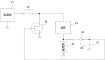
また、従来の過電流保護回路として、例えば図5に示すように、負荷43の内部の短絡故障などで負荷43に過電流が流れた場合、その過電流を抵抗器44で検知し、パルス伸長回路48を経由してスイッチング素子45を長時間オンすることで電源部41から過電流遮断型回路保護素子42へ大電流を流してこれを溶断させ、電源部41から負荷43への電源供給を停止して保護する方式が提案されている(例えば下記の特許文献2参照)。
Further, as a conventional overcurrent protection circuit, for example, as shown in FIG. 5, when an overcurrent flows through the
ところで、近年の電力変換装置は、安全性を向上させるために制御盤もしくは、箱型筐体等に収納されており、設置場所も屋内用や日射にさらされる屋外用がある。また、小動物や虫、埃、水滴等による短絡故障等を防止するために密閉状態もしくは、完全に密閉された状態で電力変換装置を構成する各回路素子を収納することがあり、そのため、電力変換装置の制御盤もしくは、箱型筐体内部の各回路素子の周囲温度が高温状態となることがある。 By the way, power converters in recent years are housed in a control panel or a box-shaped housing in order to improve safety, and are installed indoors or outdoors exposed to solar radiation. In addition, each circuit element constituting the power conversion device may be housed in a sealed state or in a completely sealed state to prevent short-circuit failures due to small animals, insects, dust, water droplets, etc. The ambient temperature of each circuit element in the control panel of the apparatus or the box-shaped housing may become a high temperature state.
上記の特許文献1記載の従来技術では、異常発生が検出された場合、高速遮断器22の補助トリップコイル39に通電されてこの高速遮断器22がオフするが、実際には、補助トリップコイル39が励磁され、その後、高速遮断器22の機械的接点が確実にオフされるまでの動作時間(例えば数ms〜数百ms)が存在する。この動作時間の間は、出力側フィルタコンデンサ28に過電圧が印加され続けるとともに、過電圧抑制サイリスタ34が連続オンしているため、入力側フィルタリアクトル23、チョッパ出力用フィルタリアクトル27、および過電圧抑制サイリスタ34といった回路素子が急激に発熱する。
In the prior art described in
この場合、上記のように周囲温度が高温状態(例えば90℃程度)であると、これら各回路素子の許容上昇温度範囲(動作保証温度)を容易に超過して回路素子が破損する課題があった。また、チョッパ回路29の出力電圧(出力側フィルタコンデンサ28の両端電圧)が非常に高い場合(例えばDC48V以上)は、一般的なトリップコイルの操作電圧(例えばDC12、24、48V)を内蔵した高速遮断器がない、もしくは、高電圧コイルとなるため、大型化するとともに高コストとなるといった課題があった。 In this case, if the ambient temperature is high as described above (for example, about 90 ° C.), there is a problem that the circuit elements are easily damaged by easily exceeding the allowable rising temperature range (operation guarantee temperature) of each circuit element. It was. In addition, when the output voltage of the chopper circuit 29 (the voltage across the output side filter capacitor 28) is very high (for example, DC48V or more), a high-speed operation incorporating a general trip coil operating voltage (for example, DC12, 24, 48V). Since there was no circuit breaker or a high voltage coil, there was a problem that the size was increased and the cost was increased.
一方、従来の特許文献2記載の過電流保護回路は、異常時、スイッチング素子45を長時間オンすることで過電流遮断型回路保護素子42を溶断させる方式であるが、特許文献1と同様に、過電流遮断型回路保護素子42が溶断するまでの時間(例えば数ms〜数百ms)が存在する。この溶断までの間は、スイッチング素子45が長時間オンしているため、当該スイッチング素子45が急激に発熱する。
On the other hand, the conventional overcurrent protection circuit described in
この場合、上記のように周囲温度が高温状態(例えば90℃程度)であると、スイッチング素子45の温度が動作保証温度を超過して破損する課題があった。また、電源部41が、定電流源であった場合は、スイッチング素子45が長時間オンしても、過電流遮断型回路保護素子42が溶断しないので保護できない、もしくは、溶断するまでの溶断時間が長くなるので、異常時、周囲温度が高温状態でなくとも、スイッチング素子45の限られた許容上昇温度範囲(動作保証温度)を容易に超過し、破損する課題があった。
In this case, when the ambient temperature is in a high temperature state (for example, about 90 ° C.) as described above, there is a problem that the temperature of the
このように、上記の特許文献1、2記載のいずれの従来技術においても、各回路素子の周囲温度が高温状態において異常が発生した場合、回路素子が破損を生じることなく安全に停止させることが難しいという課題がある。
As described above, in any of the prior arts described in
なお、特許文献1、特許文献2の構成で、周囲温度が高温状態において、異常が発生した際に回路素子が破損することなく安全に停止できるようにするためには、例えば保護動作時に発熱する各回路素子に対して放熱器を取り付けたり、放熱器を大型化することで解決できる可能性はあるものの、本来の正常動作時に必要のない放熱器が必要となることや、放熱器を過大に大型化する必要があるので、高コストになるという不具合がある。
In addition, in the configuration of
さらに、特許文献1、特許文献2共に過電圧および過電流の誤検出が発生した時は、入力を必ず遮断する構成となっている。このため、例えば雷サージ等のノイズに起因して電流検出器が誤検出したり、スイッチング素子へのノイズ混入による誤動作によって過電流(短絡)が発生するなど、電力変換装置本来の異常でない一時的な誤検出や誤動作が生じた場合でも、装置が必ず停止するため、継続して動作することができない。したがって、このような場合、従来は、再度、人手による起動、もしくは、回路素子を交換した後に再起動させることが必要で、余分な手間がかかるといった課題があった。
Further, both
この発明は、上記の課題を解決するためになされたもので、直流電源に対してDC開閉器を介して電圧変換用のスイッチング素子を有するコンバータが接続され、このコンバータで電圧変換後の直流電力を交流電力に変換するインバータが順次接続されるとともに、上記直流電源からの供給電流を検出する電流検出器と上記コンバータの出力電圧を検出する電圧検出器とを備え、これらの電流検出器と電圧検出器からの検出出力に基づいて上記コンバータとインバータの動作を制御する制御回路を備えた電力変換装置において、次の構成を採用している。 The present invention has been made to solve the above-described problem, and a converter having a voltage conversion switching element is connected to a DC power source via a DC switch, and the DC power after voltage conversion by this converter is connected. Are sequentially connected to each other, and are provided with a current detector for detecting a supply current from the DC power source and a voltage detector for detecting an output voltage of the converter. The following configuration is employed in a power conversion device including a control circuit that controls the operation of the converter and the inverter based on the detection output from the detector.
すなわち、この発明の電力変換装置は、上記制御回路が上記電流検出器による過電流の検出、あるいは上記電圧検出器による過電圧の検出に基づいて異常発生を判断した場合には、上記コンバータのスイッチング素子に流れる電流を調整して当該コンバータを構成する回路素子の発熱を抑制する発熱抑制保護手段を備えるとともに、上記制御回路は上記異常発生の判断に応じて上記DC開閉器を動作させて上記直流電源からの電力供給を遮断することを特徴としている。 That is, when the control circuit determines that an abnormality has occurred based on the detection of an overcurrent by the current detector or the detection of an overvoltage by the voltage detector, the power conversion device of the present invention provides a switching element for the converter. The control circuit includes a heat generation suppression / protection means that adjusts the current flowing through the circuit element to suppress the heat generation of the circuit elements constituting the converter, and the control circuit operates the DC switch in response to the determination of the occurrence of the abnormality. It is characterized by cutting off the power supply from.
この発明の電力変換装置によれば、制御回路が電流検出器による過電流の検出や電圧検出器による過電圧の検出に基づいて異常発生を判断した場合には、発熱抑制保護手段がコンバータのスイッチング素子に流れる電流を調整して当該コンバータを構成する回路素子の発熱を抑制して回路素子が破損に至らない状態を維持しながら、制御回路によってDC開閉器を動作させて直流電源からの電源供給を遮断できるため、筐体内部温度が高温状態であっても低コストで回路素子の破損を防止できるとともに、異常発生時に装置を安全に停止することが可能となる。 According to the power conversion device of the present invention, when the control circuit determines that an abnormality has occurred based on the detection of the overcurrent by the current detector or the detection of the overvoltage by the voltage detector, the heat generation suppression protection means is the switching element of the converter. The DC switch is operated by the control circuit to supply power from the DC power supply while maintaining the state where the circuit element is not damaged by adjusting the current flowing through the circuit and suppressing the heat generation of the circuit element constituting the converter. Since it is possible to shut off, circuit elements can be prevented from being damaged at low cost even when the temperature inside the casing is high, and the apparatus can be safely stopped when an abnormality occurs.
実施の形態1.
図1はこの発明の実施の形態1における電力変換装置の構成図である。
1 is a configuration diagram of a power conversion device according to
この実施の形態1の電力変換装置は、ここでは分散電源を系統に連系するものであって、電力変換装置の入力側には、出力電圧が最大300〜1000Vの定電流源の直流電源である太陽電池1が、DC開閉器2を介して接続されている。
The power conversion device according to the first embodiment is a system in which distributed power sources are linked to a system, and a DC power source of a constant current source having a maximum output voltage of 300 to 1000 V is provided on the input side of the power conversion device. A certain
このDC開閉器2は、その正側と負側の各接点2a、2bが手動操作によりオン(閉)されて電力変換装置に動作用の電力を供給する。また、このDC開閉器2は、電力変換装置に異常が発生した際に、太陽電池1からの電力供給を遮断して保護するためにトリップ操作コイル3を内蔵しており、後述の制御回路13からトリップ操作コイル3への操作信号Scを印加するとDC開閉器2の各接点2a、2bが共にオフ(開)する機能を備えている。
In the
DC開閉器2の後段には、太陽電池1の電圧を昇圧する昇圧コンバータ14と、この昇圧コンバータ14により昇圧された直流電圧(例えばDC300〜1000V)を交流電圧(例えばAC100V、AC200V、AC400V)に変換して交流電源(系統)11に連系するインバータ10が設けられている。
In the subsequent stage of the
ここに、上記の昇圧コンバータ14は、入力コンデンサ4、リアクトル5、スイッチング素子6、ダイオード7、および昇圧後の電圧平滑用として互いに直列に接続された第1、第2の入力コンデンサ8、9を備えている。なお、ここでは、2つのコンデンサ8、9を設けているが、耐圧を確保できるのであれば、単一のコンデンサであってもよい。また、インバータ10は三相出力でも単相出力のどちらでもよい。
Here, the
また、電力変換装置を制御するために、太陽電池1からの供給電流を検出する電流検出器15と、第1、第2の入力コンデンサ8、9の正負間の両端電圧を昇圧コンバータ14の出力電圧として検出する電圧検出器16とを備えるとともに、制御回路用電源12と制御回路13とを有する。この場合、制御回路用電源12は、入力コンデンサ4の両端に接続されて電力を取り込み制御回路13に必要な電源(例えば+5V、±15V等)を生成している。また、制御回路13は、昇圧コンバータ14のスイッチング素子6に流れる電流、電流検出器15の検出電流、電圧検出器16の検出電圧、およびインバータ10の出力電流や出力電圧の各情報に基づいて電力変換装置をマイコン等によって制御する機能を備えている。
In addition, in order to control the power conversion device, the
このような構成の電力変換装置は、安全性を向上させるために、図示しないが制御盤、もしくは、箱型筐体等に収納されており、設置場所も屋内用や日射にさらされる屋外用がある。また、小動物や虫、埃、水滴等による短絡故障等を防止するために密閉状態もしくは、完全に密閉された状態で電力変換装置を構成する各回路素子を収納することが要求されている。そのため、電力変換装置の制御盤もしくは、箱型筐体内部の回路素子の周囲温度が高温状態となることがある。このように、各回路素子の周囲温度が高温になっている状態で、昇圧コンバータ14のスイッチング素子6やインバータ10のスイッチング素子の短絡故障によって過電流が流れたり、交流電源(系統)11からの電力回生や制御回路13の動作不調などで過電圧が生じるなどの異常が発生した場合でも、回路素子が破損を生じることなく安全に停止させることが必要である。
In order to improve safety, the power conversion device having such a configuration is housed in a control panel or a box-shaped housing, etc. (not shown), and is installed indoors or outdoors exposed to sunlight. is there. In addition, in order to prevent short-circuit failures due to small animals, insects, dust, water droplets, etc., it is required to house each circuit element constituting the power converter in a sealed state or a completely sealed state. For this reason, the ambient temperature of the control panel of the power conversion device or the circuit elements inside the box-shaped housing may be in a high temperature state. As described above, in a state where the ambient temperature of each circuit element is high, an overcurrent flows due to a short circuit failure of the
そこで、この発明の実施の形態1では、上記の構成に加えて、制御回路13と昇圧コンバータ14のスイッチング素子6との間に、回路素子保護回路17および切換回路18を設けている。この場合、制御回路13は電流検出器15が過電流(短絡)を検出したり、電圧検出器16が過電圧を検出するなどの異常を検出した際、これに応じて切換回路18を動作させてゲート信号が出力される共通接点Cを通常動作時の個別接点A側から回路素子保護回路17に接続された個別接点B側に切り換える。
Therefore, in the first embodiment of the present invention, in addition to the above configuration, a circuit
また、回路素子保護回路17は、切換回路18の共通接点Cが個別接点B側に切り換えられた場合、制御回路13からスイッチング素子6に対して通常の昇圧動作時に出力されるゲート信号を例えば分周するなどして、この通常の昇圧動作時よりも低周波のゲート信号を出力するように構成されている。
Further, when the common contact C of the switching
そして、上記の切換回路18と回路素子保護回路17とによって、昇圧コンバータ14のスイッチング素子6に流れる電流を調整して当該昇圧コンバータ14を構成するリアクトル5やスイッチング素子6といった回路素子の発熱を抑制する特許請求の範囲における発熱抑制保護手段20が構成されている。
The switching
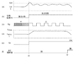
次に、上記構成の電力変換装置による各回路素子の保護動作について、図2に示すタイムチャートを参照して説明する。 Next, the protection operation of each circuit element by the power conversion device having the above configuration will be described with reference to the time chart shown in FIG.
電流検出器15の検出電流Idや電圧検出器16の検出電圧Vdが正常な場合、制御回路13は、切換回路18の共通接点Cを通常動作時の個別接点A側に接続しているので、制御回路13からは通常の昇圧動作時に出力される周波数f1(例えば10〜30kHz)のゲート信号Sgがスイッチング素子6に与えられるので、太陽電池1の電圧が昇圧コンバータ14によって所定の直流電圧(例えばDC300〜1000V)に昇圧される。
When the detection current Id of the
この状態で交流電源(系統)11からの電力回生や制御回路13の動作不調などで過電圧が生じた場合には、電圧検出器16の検出電圧Vdが基準値Vshよりも大きくなって過電圧が生じたことが制御回路13で判定される(図2(a)参照)。なお、図2では図示していないが、昇圧コンバータ14のスイッチング素子6やインバータ10のスイッチング素子の短絡故障などによって過電流が流れた場合にも、電流検出器15の検出電流Idが基準値Ishよりも大きくなって過電流が生じたことが制御回路13で判定される。
In this state, when an overvoltage occurs due to power regeneration from the AC power source (system) 11 or malfunction of the
制御回路13は、このような過電流や過電圧などの異常が発生した場合(図2の時刻t1)、これに応じて切換回路18を動作させて共通接点Cを通常動作時の個別接点A側から回路素子保護回路17に接続された個別接点B側に切り換える(図2(b)参照)。これにより、回路素子保護回路17は、制御回路13からスイッチング素子6に対して通常の昇圧動作時に出力されるゲート信号を分周するなどして、この通常の昇圧動作時の周波数f1(例えば10〜30kHz)よりも低い周波数f2(例えば1〜数kHz程度)のゲート信号Sgを出力する(図2(c)参照)。また、このとき制御回路13は、DC開閉器2のトリップ操作コイル3に接点2a、2b開放用の操作信号Scを出力する(図2(e)参照)。
When such an abnormality such as overcurrent or overvoltage occurs (time t1 in FIG. 2), the
この場合、回路素子保護回路17から出力されるゲート信号Sgの周波数f2およびオン時間(オンデューティ)は、制御回路13からDC開閉器2のトリップ操作コイル3を動作させて接点2a、2bが確実にオフされるまでの動作時間(例えば数ms〜数百ms)と、制御盤もしくは箱型筐体内部におけるリアクトル5やスイッチング素子6といった回路素子が配置された箇所の最高周囲温度を考慮して、これらのリアクトル5やスイッチング素子6の許容上昇温度範囲(動作保証温度)Tmaxを超えないように予め設定される。
In this case, the frequency f2 and on-time (on-duty) of the gate signal Sg output from the circuit
このように、異常が発生した際に電力変換装置の筐体内部温度が高温状態(例えば90℃程度)となっている場合でも、スイッチング素子6を通常の昇圧コンバータ14の周波数f1よりも低い周波数f2で動作させることで、太陽電池1から昇圧コンバータ14を構成するリアクトル5を経由してスイッチング素子6に流れる電流による発熱を調整して、リアクトル5とスイッチング素子6の許容上昇温度範囲(動作保証温度)Tmaxを越えないように抑制することができる(図2(d)参照)。
Thus, even when the internal temperature of the casing of the power conversion device is in a high temperature state (for example, about 90 ° C.) when an abnormality occurs, the switching
このように、電力変換装置の回路素子が過電圧もしくは過電流による破損が至らない状態を維持しながら、制御回路13からDC開閉器2のトリップ操作コイル3を動作させて機械的接点が確実にオフされるまでの動作時間(例えば数ms〜数百ms)が経過すると、トリップ操作コイル3が動作して接点2a、2bが共にオフ(開)になり(図2の時刻t2)、電力変換装置の動作が停止する。
Thus, the mechanical contact is reliably turned off by operating the
以上のように、この実施の形態1の電力変換装置は、その筐体内部温度が高温状態において、過電圧や過電流といった異常を検出した場合でも、各回路素子が破損することなく安全に停止することができるので、本来の正常動作時に必要のない余分な放熱器を設けるのを省略したり、あるいは放熱器を過大に大型化する必要がないため、低コストの電力変換装置を提供することができる。また、直流電源として太陽電池1のような高電圧でかつ定電流源を用いる場合であっても、回路素子を破損することなく安全に停止可能な電力変換装置を提供することができる。
As described above, the power conversion device according to the first embodiment safely stops without damaging each circuit element even when an abnormality such as overvoltage or overcurrent is detected when the temperature inside the housing is high. Therefore, it is not necessary to provide an extra heat radiator that is not necessary during normal normal operation, or it is not necessary to excessively increase the size of the heat radiator, thereby providing a low-cost power conversion device. it can. Moreover, even if it is a case where a high voltage and constant current source like the
なお、上記の説明では、過電圧や過電流といった異常が検出した場合にはスイッチング素子6に対して与えられるパルス状のゲート信号Sgを、通常の昇圧動作時に出力される周波数f1よりも低い周波数f2に切り換えるようにしているが、リアクトル5とスイッチング素子6の許容上昇温度範囲(動作保証温度)Tmaxを越えないことが確実であれば、ゲート信号Sgはパルス状のものでなく、スイッチング素子6が連続してオン動作する信号として予め設定することも可能である。
In the above description, when an abnormality such as overvoltage or overcurrent is detected, the pulse-like gate signal Sg given to the
実施の形態2.
図3はこの発明の実施の形態2における電力変換装置の構成図であり、図1に示した実施の形態1と対応もしくは相当する構成部分には同一の符号を付す。
FIG. 3 is a configuration diagram of the power conversion device according to the second embodiment of the present invention, and components corresponding to or corresponding to those of the first embodiment shown in FIG.
この実施の形態2の電力変換装置において、制御回路13は、過電流や過電圧などの異常が発生した場合、これに応じて切換回路18を動作させて共通接点Cを通常動作時の個別接点A側から回路素子保護回路17に接続された個別接点B側に切り換える点は実施の形態1と同じである。この実施の形態2の特徴は、切換回路18の切り換え時点に同時に制御回路13によって起動されて一定時間を経過した時点でタイムアップ信号を出力する時間計測回路19を備えていることである。
その他の構成は、図1に示した実施の形態1と基本的に同じであるので、ここでは詳しい説明は省略する。
In the power conversion device according to the second embodiment, when an abnormality such as an overcurrent or an overvoltage occurs, the
Since the other configuration is basically the same as that of the first embodiment shown in FIG. 1, detailed description thereof is omitted here.
この実施の形態2では、電圧検出器16の検出電圧Vdが基準値Vshよりも大きくなったり、電流検出器15の検出電流Idが基準値Ishよりも大きくなるなど、過電圧や過電流が生じたことが制御回路13で判定されると、制御回路13は、実施の形態1の場合と同様に、切換回路18を動作させて回路素子保護回路17によってスイッチング素子6に対して与えられるゲート信号Sgの周波数を低い周波数f2に切り換えることで、太陽電池1からリアクトル5を経由してスイッチング素子6に流れる電流による発熱が許容上昇温度範囲(動作保証温度)Tmaxを越えないように抑制する。
In the second embodiment, overvoltage or overcurrent has occurred, for example, the detection voltage Vd of the
この動作と並行して、制御回路13は、切換回路18を切り換え動作するのと同時に、時間計測回路19を起動して時間計測を開始する。そして、制御回路13は、一定時間を経過して時間計測回路19からタイムアップ信号が出力された際、電圧検出器16や電流検出器15によって過電圧や過電流が継続して検出されている場合には、電力変換装置本来の異常が生じているものと判断して、DC開閉器2に操作信号Scを出力する。これによってトリップ操作コイル3が動作して接点2a、2bが共にオフ(開)されて電力変換装置の動作が停止する。
In parallel with this operation, the
これに対して、制御回路13は、一定時間を経過して時間計測回路19からタイムアップ信号が出力されるまでの間に、電圧検出器16や電流検出器15による過電圧や過電流が検出されなくなった場合には、雷サージ等のノイズに起因して電流検出器15が誤検出したり、昇圧コンバータ14のスイッチング素子6へのノイズ混入による誤動作によって過電流が発生するなど、電力変換装置本来の異常でない一時的な誤検出や誤動作が生じたものと判断し、DC開閉器2には操作信号Scを出力せずにトリップ操作コイル3の接点2a、2bのオン(閉)状態を維持するとともに、切換回路18を動作させて共通接点Cを通常動作時の個別接点A側に再度切り換える。
On the other hand, the
したがって、スイッチング素子6に与えられるゲート信号Sgは、低い周波数f2から、通常の昇圧コンバータ14の昇圧動作時の高い周波数f1に復帰されることで、昇圧コンバータ14は通常の昇圧動作となる。これにより、雷サージ等のノイズに起因して電流検出器15の誤検出やインバータ10の誤動作による過電流が発生するなど、電力変換装置の本来の異常でない状態が発生した場合でも回路素子を破損することなく安全に動作を継続することができる。
Therefore, the gate signal Sg given to the
なお、この発明は、上記の実施の形態1、2の構成のみに限定されるものではなく、この発明の趣旨を逸脱しない範囲において、各実施の形態1、2の構成を適宜組み合わせたり、各実施の形態1、2の構成を変形したり、省略することが可能である。 The present invention is not limited to the configuration of the first and second embodiments described above, and the configurations of the first and second embodiments may be combined as appropriate without departing from the spirit of the present invention. The configuration of the first and second embodiments can be modified or omitted.
例えば、ここでは直流電源として、定電流源となる太陽電池1を用いた場合について説明したが、直流電源としては、これに限らず、例えばバッテリなどの直流電源やAC/DCコンバータを直流電源とする場合にも適用可能である。また、ここでは電力変換装置として昇圧コンバータ14を備えた場合について説明したが、降圧コンバータを備えた構成の場合でも適用可能である。さらに、電流検出器15は太陽電池1の負側に設けているが、正側に設けてもよい。
For example, although the case where the
1 太陽電池(直流電源)、2 DC開閉器、3 トリップ操作コイル、
4 入力コンデンサ、5 リアクトル、6 スイッチング素子、7 ダイオード、
8,9 第1、第2の入力コンデンサ、10 インバータ、11 交流電源(系統)、
12 制御回路用電源、13 制御回路、14 昇圧コンバータ、15 電流検出器、
16 電圧検出器、17 回路素子保護回路、18 切換回路、19 時間計測回路、
20 発熱抑制保護手段。
1 solar cell (DC power supply), 2 DC switch, 3 trip operation coil,
4 input capacitors, 5 reactors, 6 switching elements, 7 diodes,
8, 9 First and second input capacitors, 10 inverters, 11 AC power supply (system),
12 power supply for control circuit, 13 control circuit, 14 boost converter, 15 current detector,
16 voltage detector, 17 circuit element protection circuit, 18 switching circuit, 19 time measurement circuit,
20 Heat generation suppression protection means.
Claims (2)
上記制御回路が上記電流検出器による過電流の検出、あるいは上記電圧検出器による過電圧の検出に基づいて異常発生を判断した場合には、上記コンバータのスイッチング素子に流れる電流を調整して当該コンバータを構成する回路素子の発熱を抑制する発熱抑制保護手段を備えるとともに、上記制御回路は上記異常発生の判断に応じて上記DC開閉器を動作させて上記直流電源からの電力供給を遮断することを特徴とする電力変換装置。 A converter having a switching element for voltage conversion is connected to the DC power source via a DC switch, and an inverter for converting DC power after voltage conversion into AC power is sequentially connected by this converter, and the DC power source A current detector that detects the supply current from the power supply and a voltage detector that detects the output voltage of the converter, and controls the operation of the converter and the inverter based on the detection output from the current detector and the voltage detector. In the power conversion device including the control circuit to
When the control circuit determines that an abnormality has occurred based on the detection of an overcurrent by the current detector or the detection of an overvoltage by the voltage detector, the current flowing through the switching element of the converter is adjusted to In addition to heat generation suppression protection means for suppressing heat generation of the circuit elements that constitute the circuit element, the control circuit operates the DC switch according to the determination of the occurrence of the abnormality to cut off the power supply from the DC power supply. A power converter.
Priority Applications (1)
| Application Number | Priority Date | Filing Date | Title |
|---|---|---|---|
| JP2012143590A JP2014007909A (en) | 2012-06-27 | 2012-06-27 | Power conversion apparatus |
Applications Claiming Priority (1)
| Application Number | Priority Date | Filing Date | Title |
|---|---|---|---|
| JP2012143590A JP2014007909A (en) | 2012-06-27 | 2012-06-27 | Power conversion apparatus |
Publications (1)
| Publication Number | Publication Date |
|---|---|
| JP2014007909A true JP2014007909A (en) | 2014-01-16 |
Family
ID=50105190
Family Applications (1)
| Application Number | Title | Priority Date | Filing Date |
|---|---|---|---|
| JP2012143590A Pending JP2014007909A (en) | 2012-06-27 | 2012-06-27 | Power conversion apparatus |
Country Status (1)
| Country | Link |
|---|---|
| JP (1) | JP2014007909A (en) |
Cited By (5)
| Publication number | Priority date | Publication date | Assignee | Title |
|---|---|---|---|---|
| JP2015154508A (en) * | 2014-02-10 | 2015-08-24 | 三菱電機株式会社 | System interlocked inverter |
| WO2018073892A1 (en) * | 2016-10-18 | 2018-04-26 | 富士機械製造株式会社 | Non-contact power supply device |
| JP2019134602A (en) * | 2018-01-31 | 2019-08-08 | ニチコン株式会社 | Power unit |
| JP2019154106A (en) * | 2018-03-01 | 2019-09-12 | 新電元工業株式会社 | Power conditioner system |
| JPWO2022091250A1 (en) * | 2020-10-28 | 2022-05-05 |
Citations (5)
| Publication number | Priority date | Publication date | Assignee | Title |
|---|---|---|---|---|
| JP2004048983A (en) * | 2002-05-23 | 2004-02-12 | Toyota Motor Corp | Motor driving device, control method of motor driving device, and recording medium with program record thereon for causing computer to control motor driving device |
| JP2007252134A (en) * | 2006-03-17 | 2007-09-27 | Toyota Motor Corp | Load driver and automobile mounting it |
| JP2009100507A (en) * | 2007-10-15 | 2009-05-07 | Toyota Motor Corp | Load drive device, electric vehicle, method of controlling load drive device, and computer-readable recording medium recording program for causing computer to execute this control method |
| JP2009273280A (en) * | 2008-05-09 | 2009-11-19 | Hitachi Ltd | Dc-dc converter |
| US20110307136A1 (en) * | 2009-02-25 | 2011-12-15 | Toyota Jidosha Kabushiki Kaisha | Device and method for controlling vehicle |
-
2012
- 2012-06-27 JP JP2012143590A patent/JP2014007909A/en active Pending
Patent Citations (5)
| Publication number | Priority date | Publication date | Assignee | Title |
|---|---|---|---|---|
| JP2004048983A (en) * | 2002-05-23 | 2004-02-12 | Toyota Motor Corp | Motor driving device, control method of motor driving device, and recording medium with program record thereon for causing computer to control motor driving device |
| JP2007252134A (en) * | 2006-03-17 | 2007-09-27 | Toyota Motor Corp | Load driver and automobile mounting it |
| JP2009100507A (en) * | 2007-10-15 | 2009-05-07 | Toyota Motor Corp | Load drive device, electric vehicle, method of controlling load drive device, and computer-readable recording medium recording program for causing computer to execute this control method |
| JP2009273280A (en) * | 2008-05-09 | 2009-11-19 | Hitachi Ltd | Dc-dc converter |
| US20110307136A1 (en) * | 2009-02-25 | 2011-12-15 | Toyota Jidosha Kabushiki Kaisha | Device and method for controlling vehicle |
Cited By (10)
| Publication number | Priority date | Publication date | Assignee | Title |
|---|---|---|---|---|
| JP2015154508A (en) * | 2014-02-10 | 2015-08-24 | 三菱電機株式会社 | System interlocked inverter |
| WO2018073892A1 (en) * | 2016-10-18 | 2018-04-26 | 富士機械製造株式会社 | Non-contact power supply device |
| CN109792162A (en) * | 2016-10-18 | 2019-05-21 | 株式会社富士 | Contactless power supply device |
| JPWO2018073892A1 (en) * | 2016-10-18 | 2019-08-08 | 株式会社Fuji | Non-contact power feeding device |
| JP2019134602A (en) * | 2018-01-31 | 2019-08-08 | ニチコン株式会社 | Power unit |
| JP2019154106A (en) * | 2018-03-01 | 2019-09-12 | 新電元工業株式会社 | Power conditioner system |
| JP7009261B2 (en) | 2018-03-01 | 2022-01-25 | 新電元工業株式会社 | Power conditioner system |
| JPWO2022091250A1 (en) * | 2020-10-28 | 2022-05-05 | ||
| WO2022091250A1 (en) * | 2020-10-28 | 2022-05-05 | 東芝三菱電機産業システム株式会社 | Protection system, solar power generation system, and protection method |
| JP7384224B2 (en) | 2020-10-28 | 2023-11-21 | 東芝三菱電機産業システム株式会社 | Solar power generation system and protection method for solar power generation system |
Similar Documents
| Publication | Publication Date | Title |
|---|---|---|
| JP5115829B2 (en) | Switching device | |
| JP4942143B2 (en) | Inverter device and overvoltage protection method thereof | |
| US20110194216A1 (en) | Protection Circuit for Protecting an Intermediate Circuit of a Solar Inverter Against Overvoltages | |
| JP2003134661A (en) | Load interruption detecting device and photovoltaic power generator | |
| JP5728914B2 (en) | Inverter device | |
| JP2014007909A (en) | Power conversion apparatus | |
| JP2017502490A (en) | Voltage clipping | |
| JP2004289159A (en) | Circuit structure, additional module and solar device system | |
| JP2010268625A (en) | Power supply system | |
| WO2007096994A1 (en) | System-cooperative inverter | |
| WO2013051351A1 (en) | Switching power supply circuit with protective function | |
| JP2008252966A (en) | Motor drive device | |
| JP5743913B2 (en) | Power converter | |
| KR20150063941A (en) | Method for the operation of a pitch system of a wind turbine | |
| JP2008054483A (en) | Instantaneous voltage drop compensator | |
| EP3120434B1 (en) | Power supply stage of an electric appliance, in particular a battery charger for charging batteries of electric vehicles | |
| JP2016157364A (en) | Power control unit and control method thereof | |
| JP2015006074A (en) | Power conversion device | |
| JP5332621B2 (en) | Uninterruptible power system | |
| JP6285167B2 (en) | Thyristor type high voltage automatic voltage regulator | |
| JP2017143607A (en) | Shunt device, electric power system, and space structure | |
| JP2005268258A (en) | Power converter | |
| JP2007252164A (en) | Distributed power supply system | |
| JP6455719B2 (en) | Uninterruptible power supply system | |
| TWI792532B (en) | Protection control method for suppressing inrush current and protection control system thereof |
Legal Events
| Date | Code | Title | Description |
|---|---|---|---|
| A621 | Written request for application examination |
Free format text: JAPANESE INTERMEDIATE CODE: A621 Effective date: 20140930 |
|
| A131 | Notification of reasons for refusal |
Free format text: JAPANESE INTERMEDIATE CODE: A131 Effective date: 20150623 |
|
| A977 | Report on retrieval |
Free format text: JAPANESE INTERMEDIATE CODE: A971007 Effective date: 20150624 |
|
| A02 | Decision of refusal |
Free format text: JAPANESE INTERMEDIATE CODE: A02 Effective date: 20151020 |