JP2013512556A - Optoelectronic component housing and housing manufacturing method - Google Patents
Optoelectronic component housing and housing manufacturing method Download PDFInfo
- Publication number
- JP2013512556A JP2013512556A JP2012540348A JP2012540348A JP2013512556A JP 2013512556 A JP2013512556 A JP 2013512556A JP 2012540348 A JP2012540348 A JP 2012540348A JP 2012540348 A JP2012540348 A JP 2012540348A JP 2013512556 A JP2013512556 A JP 2013512556A
- Authority
- JP
- Japan
- Prior art keywords
- plastic material
- coating
- housing
- housing body
- housing according
- Prior art date
- Legal status (The legal status is an assumption and is not a legal conclusion. Google has not performed a legal analysis and makes no representation as to the accuracy of the status listed.)
- Pending
Links
- 230000005693 optoelectronics Effects 0.000 title claims abstract description 36
- 238000004519 manufacturing process Methods 0.000 title claims description 11
- 239000000463 material Substances 0.000 claims abstract description 151
- 239000004033 plastic Substances 0.000 claims abstract description 116
- 229920003023 plastic Polymers 0.000 claims abstract description 116
- 238000000576 coating method Methods 0.000 claims abstract description 113
- 239000011248 coating agent Substances 0.000 claims abstract description 110
- 230000005670 electromagnetic radiation Effects 0.000 claims abstract description 23
- 230000005855 radiation Effects 0.000 claims description 18
- 238000001746 injection moulding Methods 0.000 claims description 17
- 239000004065 semiconductor Substances 0.000 claims description 13
- 230000003287 optical effect Effects 0.000 claims description 12
- 239000012463 white pigment Substances 0.000 claims description 11
- GWEVSGVZZGPLCZ-UHFFFAOYSA-N Titan oxide Chemical compound O=[Ti]=O GWEVSGVZZGPLCZ-UHFFFAOYSA-N 0.000 claims description 10
- 238000002845 discoloration Methods 0.000 claims description 10
- 230000008878 coupling Effects 0.000 claims description 8
- 238000010168 coupling process Methods 0.000 claims description 8
- 238000005859 coupling reaction Methods 0.000 claims description 8
- 238000002347 injection Methods 0.000 claims description 7
- 239000007924 injection Substances 0.000 claims description 7
- 229920000106 Liquid crystal polymer Polymers 0.000 claims description 6
- 239000004977 Liquid-crystal polymers (LCPs) Substances 0.000 claims description 6
- 239000004952 Polyamide Substances 0.000 claims description 6
- 229920002647 polyamide Polymers 0.000 claims description 6
- 229920001296 polysiloxane Polymers 0.000 claims description 6
- 238000002310 reflectometry Methods 0.000 claims description 6
- 239000004696 Poly ether ether ketone Substances 0.000 claims description 5
- 238000000034 method Methods 0.000 claims description 5
- 229920002530 polyetherether ketone Polymers 0.000 claims description 5
- 239000004697 Polyetherimide Substances 0.000 claims description 4
- 239000004734 Polyphenylene sulfide Substances 0.000 claims description 4
- 229920000491 Polyphenylsulfone Polymers 0.000 claims description 4
- 239000004954 Polyphthalamide Substances 0.000 claims description 4
- XLOMVQKBTHCTTD-UHFFFAOYSA-N Zinc monoxide Chemical compound [Zn]=O XLOMVQKBTHCTTD-UHFFFAOYSA-N 0.000 claims description 4
- MCMNRKCIXSYSNV-UHFFFAOYSA-N Zirconium dioxide Chemical compound O=[Zr]=O MCMNRKCIXSYSNV-UHFFFAOYSA-N 0.000 claims description 4
- TZCXTZWJZNENPQ-UHFFFAOYSA-L barium sulfate Chemical compound [Ba+2].[O-]S([O-])(=O)=O TZCXTZWJZNENPQ-UHFFFAOYSA-L 0.000 claims description 4
- 230000006378 damage Effects 0.000 claims description 4
- -1 lithopone Chemical compound 0.000 claims description 4
- 229920001601 polyetherimide Polymers 0.000 claims description 4
- 229920000069 polyphenylene sulfide Polymers 0.000 claims description 4
- 229920006375 polyphtalamide Polymers 0.000 claims description 4
- 239000004408 titanium dioxide Substances 0.000 claims description 4
- JUPQTSLXMOCDHR-UHFFFAOYSA-N benzene-1,4-diol;bis(4-fluorophenyl)methanone Chemical compound OC1=CC=C(O)C=C1.C1=CC(F)=CC=C1C(=O)C1=CC=C(F)C=C1 JUPQTSLXMOCDHR-UHFFFAOYSA-N 0.000 claims description 3
- 229920002313 fluoropolymer Polymers 0.000 claims description 3
- 239000004811 fluoropolymer Substances 0.000 claims description 3
- 229920001643 poly(ether ketone) Polymers 0.000 claims description 3
- 229920000728 polyester Polymers 0.000 claims description 3
- 229910052582 BN Inorganic materials 0.000 claims description 2
- PZNSFCLAULLKQX-UHFFFAOYSA-N Boron nitride Chemical compound N#B PZNSFCLAULLKQX-UHFFFAOYSA-N 0.000 claims description 2
- 239000005083 Zinc sulfide Substances 0.000 claims description 2
- PNEYBMLMFCGWSK-UHFFFAOYSA-N aluminium oxide Inorganic materials [O-2].[O-2].[O-2].[Al+3].[Al+3] PNEYBMLMFCGWSK-UHFFFAOYSA-N 0.000 claims description 2
- 239000011787 zinc oxide Substances 0.000 claims description 2
- 229910052984 zinc sulfide Inorganic materials 0.000 claims description 2
- DRDVZXDWVBGGMH-UHFFFAOYSA-N zinc;sulfide Chemical compound [S-2].[Zn+2] DRDVZXDWVBGGMH-UHFFFAOYSA-N 0.000 claims description 2
- 239000000945 filler Substances 0.000 description 9
- 238000005266 casting Methods 0.000 description 7
- 239000002245 particle Substances 0.000 description 6
- 238000002844 melting Methods 0.000 description 5
- 230000008018 melting Effects 0.000 description 5
- 239000003365 glass fiber Substances 0.000 description 4
- 239000000853 adhesive Substances 0.000 description 3
- 230000001070 adhesive effect Effects 0.000 description 3
- 239000011256 inorganic filler Substances 0.000 description 3
- 229910003475 inorganic filler Inorganic materials 0.000 description 3
- 229920006153 PA4T Polymers 0.000 description 2
- 230000032683 aging Effects 0.000 description 2
- 239000006229 carbon black Substances 0.000 description 2
- 239000000049 pigment Substances 0.000 description 2
- 229910000679 solder Inorganic materials 0.000 description 2
- 238000005476 soldering Methods 0.000 description 2
- 229910018072 Al 2 O 3 Inorganic materials 0.000 description 1
- 239000004956 Amodel Substances 0.000 description 1
- 208000015943 Coeliac disease Diseases 0.000 description 1
- 229920006060 Grivory® Polymers 0.000 description 1
- 229920003189 Nylon 4,6 Polymers 0.000 description 1
- 229920006106 Zytel® HTN Polymers 0.000 description 1
- 230000002745 absorbent Effects 0.000 description 1
- 239000002250 absorbent Substances 0.000 description 1
- 239000011358 absorbing material Substances 0.000 description 1
- 238000004026 adhesive bonding Methods 0.000 description 1
- 238000006243 chemical reaction Methods 0.000 description 1
- PMHQVHHXPFUNSP-UHFFFAOYSA-M copper(1+);methylsulfanylmethane;bromide Chemical compound Br[Cu].CSC PMHQVHHXPFUNSP-UHFFFAOYSA-M 0.000 description 1
- 239000000835 fiber Substances 0.000 description 1
- 239000001023 inorganic pigment Substances 0.000 description 1
- 239000007788 liquid Substances 0.000 description 1
- 238000004020 luminiscence type Methods 0.000 description 1
- 239000000155 melt Substances 0.000 description 1
- 239000012528 membrane Substances 0.000 description 1
- 229920006119 nylon 10T Polymers 0.000 description 1
- 229920006139 poly(hexamethylene adipamide-co-hexamethylene terephthalamide) Polymers 0.000 description 1
- 229920006111 poly(hexamethylene terephthalamide) Polymers 0.000 description 1
- 239000004810 polytetrafluoroethylene Substances 0.000 description 1
- 229920001343 polytetrafluoroethylene Polymers 0.000 description 1
- 230000035882 stress Effects 0.000 description 1
- 239000012815 thermoplastic material Substances 0.000 description 1
- 238000004383 yellowing Methods 0.000 description 1
Images


Classifications
-
- H—ELECTRICITY
- H01—ELECTRIC ELEMENTS
- H01L—SEMICONDUCTOR DEVICES NOT COVERED BY CLASS H10
- H01L31/00—Semiconductor devices sensitive to infrared radiation, light, electromagnetic radiation of shorter wavelength or corpuscular radiation and specially adapted either for the conversion of the energy of such radiation into electrical energy or for the control of electrical energy by such radiation; Processes or apparatus specially adapted for the manufacture or treatment thereof or of parts thereof; Details thereof
- H01L31/02—Details
- H01L31/0203—Containers; Encapsulations, e.g. encapsulation of photodiodes
-
- H—ELECTRICITY
- H01—ELECTRIC ELEMENTS
- H01L—SEMICONDUCTOR DEVICES NOT COVERED BY CLASS H10
- H01L33/00—Semiconductor devices with at least one potential-jump barrier or surface barrier specially adapted for light emission; Processes or apparatus specially adapted for the manufacture or treatment thereof or of parts thereof; Details thereof
- H01L33/44—Semiconductor devices with at least one potential-jump barrier or surface barrier specially adapted for light emission; Processes or apparatus specially adapted for the manufacture or treatment thereof or of parts thereof; Details thereof characterised by the coatings, e.g. passivation layer or anti-reflective coating
-
- H—ELECTRICITY
- H01—ELECTRIC ELEMENTS
- H01L—SEMICONDUCTOR DEVICES NOT COVERED BY CLASS H10
- H01L33/00—Semiconductor devices with at least one potential-jump barrier or surface barrier specially adapted for light emission; Processes or apparatus specially adapted for the manufacture or treatment thereof or of parts thereof; Details thereof
- H01L33/48—Semiconductor devices with at least one potential-jump barrier or surface barrier specially adapted for light emission; Processes or apparatus specially adapted for the manufacture or treatment thereof or of parts thereof; Details thereof characterised by the semiconductor body packages
- H01L33/483—Containers
- H01L33/486—Containers adapted for surface mounting
-
- H—ELECTRICITY
- H01—ELECTRIC ELEMENTS
- H01L—SEMICONDUCTOR DEVICES NOT COVERED BY CLASS H10
- H01L33/00—Semiconductor devices with at least one potential-jump barrier or surface barrier specially adapted for light emission; Processes or apparatus specially adapted for the manufacture or treatment thereof or of parts thereof; Details thereof
- H01L33/48—Semiconductor devices with at least one potential-jump barrier or surface barrier specially adapted for light emission; Processes or apparatus specially adapted for the manufacture or treatment thereof or of parts thereof; Details thereof characterised by the semiconductor body packages
- H01L33/52—Encapsulations
- H01L33/56—Materials, e.g. epoxy or silicone resin
-
- H—ELECTRICITY
- H01—ELECTRIC ELEMENTS
- H01L—SEMICONDUCTOR DEVICES NOT COVERED BY CLASS H10
- H01L2224/00—Indexing scheme for arrangements for connecting or disconnecting semiconductor or solid-state bodies and methods related thereto as covered by H01L24/00
- H01L2224/01—Means for bonding being attached to, or being formed on, the surface to be connected, e.g. chip-to-package, die-attach, "first-level" interconnects; Manufacturing methods related thereto
- H01L2224/42—Wire connectors; Manufacturing methods related thereto
- H01L2224/47—Structure, shape, material or disposition of the wire connectors after the connecting process
- H01L2224/48—Structure, shape, material or disposition of the wire connectors after the connecting process of an individual wire connector
- H01L2224/481—Disposition
- H01L2224/48151—Connecting between a semiconductor or solid-state body and an item not being a semiconductor or solid-state body, e.g. chip-to-substrate, chip-to-passive
- H01L2224/48221—Connecting between a semiconductor or solid-state body and an item not being a semiconductor or solid-state body, e.g. chip-to-substrate, chip-to-passive the body and the item being stacked
- H01L2224/48245—Connecting between a semiconductor or solid-state body and an item not being a semiconductor or solid-state body, e.g. chip-to-substrate, chip-to-passive the body and the item being stacked the item being metallic
- H01L2224/48247—Connecting between a semiconductor or solid-state body and an item not being a semiconductor or solid-state body, e.g. chip-to-substrate, chip-to-passive the body and the item being stacked the item being metallic connecting the wire to a bond pad of the item
-
- H—ELECTRICITY
- H01—ELECTRIC ELEMENTS
- H01L—SEMICONDUCTOR DEVICES NOT COVERED BY CLASS H10
- H01L2924/00—Indexing scheme for arrangements or methods for connecting or disconnecting semiconductor or solid-state bodies as covered by H01L24/00
- H01L2924/15—Details of package parts other than the semiconductor or other solid state devices to be connected
- H01L2924/181—Encapsulation
-
- H—ELECTRICITY
- H01—ELECTRIC ELEMENTS
- H01L—SEMICONDUCTOR DEVICES NOT COVERED BY CLASS H10
- H01L2924/00—Indexing scheme for arrangements or methods for connecting or disconnecting semiconductor or solid-state bodies as covered by H01L24/00
- H01L2924/30—Technical effects
- H01L2924/301—Electrical effects
- H01L2924/3025—Electromagnetic shielding
-
- H—ELECTRICITY
- H01—ELECTRIC ELEMENTS
- H01L—SEMICONDUCTOR DEVICES NOT COVERED BY CLASS H10
- H01L33/00—Semiconductor devices with at least one potential-jump barrier or surface barrier specially adapted for light emission; Processes or apparatus specially adapted for the manufacture or treatment thereof or of parts thereof; Details thereof
- H01L33/48—Semiconductor devices with at least one potential-jump barrier or surface barrier specially adapted for light emission; Processes or apparatus specially adapted for the manufacture or treatment thereof or of parts thereof; Details thereof characterised by the semiconductor body packages
- H01L33/58—Optical field-shaping elements
- H01L33/60—Reflective elements
-
- H—ELECTRICITY
- H01—ELECTRIC ELEMENTS
- H01L—SEMICONDUCTOR DEVICES NOT COVERED BY CLASS H10
- H01L33/00—Semiconductor devices with at least one potential-jump barrier or surface barrier specially adapted for light emission; Processes or apparatus specially adapted for the manufacture or treatment thereof or of parts thereof; Details thereof
- H01L33/48—Semiconductor devices with at least one potential-jump barrier or surface barrier specially adapted for light emission; Processes or apparatus specially adapted for the manufacture or treatment thereof or of parts thereof; Details thereof characterised by the semiconductor body packages
- H01L33/64—Heat extraction or cooling elements
- H01L33/641—Heat extraction or cooling elements characterized by the materials
Abstract
本発明は、オプトエレクトロニクス部品(7)のハウジング(1)に関し、このハウジングは、凹部(4)を有するハウジング本体(2)と、コーティング(3)と、を備えている。コーティング(3)は、少なくとも凹部(4)の領域において、少なくとも部分的にハウジング本体(2)に結合されており、かつハウジング本体(2)に直接接触している。ハウジング本体(2)は第1のプラスチック材料から形成されており、コーティング(3)は第2のプラスチック材料から形成されており、第1のプラスチック材料は第2のプラスチック材料と異なり、第1のプラスチック材料および第2のプラスチック材料は、材料特性として、温度耐性、および電磁放射に対する耐性、のうちの少なくとも一方に関して、互いに異なる。The present invention relates to a housing (1) for an optoelectronic component (7), which comprises a housing body (2) having a recess (4) and a coating (3). The coating (3) is at least partially coupled to the housing body (2) and is in direct contact with the housing body (2), at least in the region of the recess (4). The housing body (2) is formed from a first plastic material, the coating (3) is formed from a second plastic material, the first plastic material being different from the second plastic material, The plastic material and the second plastic material differ from each other in terms of material properties, at least one of temperature resistance and resistance to electromagnetic radiation.
Description
本発明の目的は、オプトエレクトロニクス部品のハウジングであって、経年劣化に対する耐性が高く、それと同時に光学特性が改善されたハウジング、を提供することである。 It is an object of the present invention to provide an optoelectronic component housing that is highly resistant to aging and at the same time has improved optical properties.
オプトエレクトロニクス部品のハウジングを提供する。オプトエレクトロニクス部品は、例えば、オプトエレクトロニクス半導体チップである。オプトエレクトロニクス半導体チップは、放射受信チップまたは放射放出チップとすることができる。ハウジングは、例えば、少なくとも1個の発光ダイオードチップ、少なくとも1個のレーザダイオードチップ、または少なくとも1個フォトダイオードチップ、もしくはこれらのうちの2種類以上、のハウジングとすることができる。 Provide optoelectronic component housing. The optoelectronic component is, for example, an optoelectronic semiconductor chip. The optoelectronic semiconductor chip can be a radiation receiving chip or a radiation emitting chip. The housing can be, for example, at least one light emitting diode chip, at least one laser diode chip, or at least one photodiode chip, or two or more of these.
本ハウジングの少なくとも一実施形態によると、ハウジングは、凹部を有するハウジング本体を備えている。ハウジング本体の凹部は、少なくとも1つのオプトエレクトロニクス部品を受け入れる目的に適するように形成されている。凹部は、例えば、凹部の横方向の境界を形成する側壁であって、ハウジングの中に配置されたオプトエレクトロニクス部品を横方向に囲んでいる側壁、を有することができる。 According to at least one embodiment of the housing, the housing includes a housing body having a recess. The recess of the housing body is formed to be suitable for the purpose of receiving at least one optoelectronic component. The recess can have, for example, a sidewall that forms a lateral boundary of the recess and that laterally surrounds the optoelectronic component disposed in the housing.
本ハウジングの少なくとも一実施形態によると、ハウジングはコーティングを備えており、このコーティングは、少なくとも凹部の領域において、少なくとも部分的にハウジング本体に結合されており、かつハウジング本体に直接接触している。したがって、コーティングはハウジングの一部であり、例えば、ハウジング本体の外側領域に直接形成されている。この場合、コーティングは、少なくとも凹部の領域に存在する。例えば、凹部の領域においてハウジング本体をコーティングによって完全に覆うことができる。さらには、ハウジング本体の凹部の側面領域のみ、または側面領域の一部分のみをコーティングによって覆い、凹部のそれ以外の領域(例えば底部領域)にはコーティングが存在しない、または実質的に存在しないようにすることが可能である。「コーティングが実質的に存在しない」とは、例えば、凹部の底部領域のうちコーティングによって覆われている表面積の割合が、最大で20%、特に最大で10%であることを意味する。 According to at least one embodiment of the housing, the housing comprises a coating that is at least partially coupled to and in direct contact with the housing body, at least in the region of the recess. Thus, the coating is part of the housing, for example formed directly on the outer region of the housing body. In this case, the coating is present at least in the area of the recess. For example, the housing body can be completely covered with a coating in the region of the recess. Furthermore, only the side surface region or only a part of the side surface region of the recess of the housing body is covered with the coating so that the coating is not present or substantially absent in other regions (for example, the bottom region) of the recess. It is possible. “Substantially no coating” means, for example, that the proportion of the surface area covered by the coating in the bottom region of the recess is at most 20%, in particular at most 10%.
コーティングは、特に均一な厚さを有する。これは、特に、製造ばらつきの範囲内で、コーティング全体にわたりコーティングの厚さが変化しないことを意味する。 The coating has a particularly uniform thickness. This means in particular that the thickness of the coating does not change throughout the coating within the range of manufacturing variability.
コーティングはハウジング本体に結合されており、この場合、ハウジング本体からコーティングを剥離するとコーティングもしくはハウジング本体またはその両方が破壊されるような機械的強さで、結合されていることが好ましい。言い換えれば、ハウジング本体とコーティングは、破壊しない限りは分離することのできないユニットを形成している。 The coating is bonded to the housing body, preferably in such a way that the mechanical strength is such that peeling the coating from the housing body will destroy the coating and / or the housing body. In other words, the housing body and the coating form a unit that cannot be separated unless destroyed.
本ハウジングの少なくとも一実施形態によると、ハウジング本体が第1のプラスチック材料によって形成されており、コーティングが第2のプラスチック材料によって形成されており、第1のプラスチック材料は第2のプラスチック材料と異なる。すなわち、ハウジング本体とコーティングは、異なる材料から形成されている。ハウジング本体とコーティングは、異なるプラスチック材料から形成されていることが好ましく、この場合、ハウジング本体のプラスチック材料とコーティングのプラスチック材料が同じ成分を有し、ただし少なくとも1種類の成分が互いに異なっていることも可能である。 According to at least one embodiment of the housing, the housing body is formed of a first plastic material, the coating is formed of a second plastic material, and the first plastic material is different from the second plastic material. . That is, the housing body and the coating are formed from different materials. The housing body and the coating are preferably made of different plastic materials, in which case the plastic material of the housing body and the plastic material of the coating have the same components, but at least one component is different from each other Is also possible.
本ハウジングの少なくとも一実施形態によると、第1のプラスチック材料と第2のプラスチック材料は、以下の材料特性、すなわち、
変色に関する温度耐性、
変形に関する温度耐性、
破壊に関する温度耐性、
電磁放射に対する耐性、
のうちの少なくとも1つに関して、互いに異なる。
According to at least one embodiment of the housing, the first plastic material and the second plastic material have the following material properties:
Temperature tolerance for discoloration,
Temperature tolerance for deformation,
Temperature resistance for destruction,
Resistance to electromagnetic radiation,
Are different from each other with respect to at least one of them.
温度耐性とは、本明細書においては、特に次のように理解される。すなわち、温度耐性の高いプラスチック材料は、特に、変色、変形、または破壊が生じる限界温度が、温度耐性の低いプラスチック材料よりも高い。これに代えて、またはこれに加えて、温度耐性の高いプラスチック材料は、特定の温度において、変形、変色、または破壊に対して、温度耐性の低いプラスチック材料よりも長い時間にわたり耐えることができる。なお、あるプラスチック材料が、例えば変色に対しては別のプラスチック材料よりも長い時間にわたり耐えるが、変形に関してはその別のプラスチック材料よりも耐性が低いことがある。 In the present specification, the temperature resistance is understood as follows. That is, a plastic material having a high temperature resistance has a higher limit temperature at which discoloration, deformation, or destruction occurs, in particular, than a plastic material having a low temperature resistance. Alternatively or in addition, a temperature resistant plastic material can withstand a longer time than a less temperature resistant plastic material at a particular temperature against deformation, discoloration, or failure. It should be noted that a plastic material may withstand, for example, discoloration for a longer time than another plastic material, but may be less resistant to deformation than the other plastic material.
電磁放射に対する耐性とは、特に次のように理解される。すなわち、2種類のプラスチック材料が同じ条件で電磁放射にさらされた場合、電磁放射に対する耐性の高い材料は、電磁放射に対する耐性の低いプラスチック材料よりも時間的に後から変色または変形する。電磁放射とは、例えば、紫外線または青色光の波長域の電磁放射である。この場合、特に、電磁放射に対する耐性の高いプラスチック材料の変色は、電磁放射に対する耐性の低い材料と比較して、時間的に遅れて発生する。 Resistance to electromagnetic radiation is understood in particular as follows. That is, when two types of plastic material are exposed to electromagnetic radiation under the same conditions, a material that is more resistant to electromagnetic radiation will discolor or deform later in time than a plastic material that is less resistant to electromagnetic radiation. The electromagnetic radiation is, for example, electromagnetic radiation in the wavelength range of ultraviolet light or blue light. In this case, in particular, the discoloration of the plastic material that is highly resistant to electromagnetic radiation occurs later in time than the material that is less resistant to electromagnetic radiation.
オプトエレクトロニクス部品の本ハウジングの少なくとも一実施形態によると、ハウジングは、凹部を有するハウジング本体と、コーティングを備えている。コーティングは、少なくとも凹部の領域において少なくとも部分的にハウジング本体に結合されており、かつハウジング本体に直接接触している。ハウジング本体は第1のプラスチック材料によって形成されており、コーティングは第2のプラスチック材料によって形成されている。第1のプラスチック材料は第2のプラスチック材料と異なり、第1のプラスチック材料と第2のプラスチック材料は、以下の材料特性、すなわち、
変色に関する温度耐性、
変形に関する温度耐性、
破壊に関する温度耐性、
電磁放射に対する耐性、
のうちの少なくとも1つに関して、互いに異なる。
According to at least one embodiment of the present optoelectronic component housing, the housing comprises a housing body having a recess and a coating. The coating is at least partially coupled to the housing body at least in the region of the recess and is in direct contact with the housing body. The housing body is made of a first plastic material and the coating is made of a second plastic material. The first plastic material is different from the second plastic material, and the first plastic material and the second plastic material have the following material properties:
Temperature tolerance for discoloration,
Temperature tolerance for deformation,
Temperature resistance for destruction,
Resistance to electromagnetic radiation,
Are different from each other with respect to at least one of them.
本明細書に記載されているハウジングの場合、特に、温度耐性の高いプラスチック材料が、電磁放射に対して低い耐性を有することが可能である。また、同じプラスチック材料を使用し、ハウジング本体とコーティングの異なる特性を、プラスチック材料中の充填材によって調節することも、理論的には可能である。さらに、再生プラスチックは安定性が低く、実際にハウジングに使用するうえで適さない色を有することがあるが、特に、ハウジング本体に再生プラスチックを使用することが可能である。したがって、本明細書に記載されているハウジングは、特に低コスト、かつ環境に対して特に小さい影響で、製造することができる。 In the case of the housing described herein, in particular, a temperature-resistant plastic material can have a low resistance to electromagnetic radiation. It is also theoretically possible to use the same plastic material and to adjust the different properties of the housing body and the coating by the filler in the plastic material. Furthermore, recycled plastics are less stable and may have a color that is not suitable for practical use in a housing, but it is possible to use recycled plastics in particular for the housing body. Thus, the housing described herein can be manufactured with a particularly low cost and a particularly small impact on the environment.
本ハウジングの少なくとも一実施形態によると、ハウジングの本体およびコーティングは、それぞれの光学特性に関して互いに異なる。しかしながら、ハウジング本体のプラスチック材料とコーティングのプラスチック材料は、それぞれの光学特性が必ずしも互いに異なっていなくてもよい。その場合、ハウジング本体もしくはコーティングまたはその両方の光学特性を、第1のプラスチック材料もしくは第2のプラスチック材料またはその両方に含まれる充填材によって、個別に調整することができる。例えば、特定の波長域の電磁放射を反射するようにコーティングを調整し、同じ波長域または別の波長域の放射を吸収するようにハウジング本体を構成することができる。しかしながら、プラスチック材料(すなわち第1のプラスチック材料および第2のプラスチック材料)が、互いに異なる光学特性を有することも可能である。この場合、ハウジング本体およびコーティングを形成する第1のプラスチック材料および第2のプラスチック材料のいずれにも充填材を含めないことが可能である。この場合、ハウジング本体が第1のプラスチック材料からなり、コーティングが第2のプラスチック材料からなることができる。 According to at least one embodiment of the housing, the housing body and the coating are different from each other with respect to their respective optical properties. However, the plastic material of the housing body and the plastic material of the coating do not necessarily have to have different optical properties. In that case, the optical properties of the housing body and / or coating can be individually adjusted by the filler contained in the first plastic material and / or the second plastic material. For example, the housing body can be configured to adjust the coating to reflect electromagnetic radiation in a particular wavelength range and absorb radiation in the same wavelength range or another wavelength range. However, it is also possible that the plastic materials (ie the first plastic material and the second plastic material) have different optical properties. In this case, it is possible that neither the first plastic material nor the second plastic material forming the housing body and the coating contains a filler. In this case, the housing body can be made of a first plastic material and the coating can be made of a second plastic material.
本ハウジングの少なくとも一実施形態によると、コーティングは、紫外線放射に対する80%以上の反射率を有する。これは、コーティングの反射率が、紫外線領域の少なくとも1つの波長に対して80%以上であることを意味する。コーティングの反射率は、好ましくは90%以上、特に好ましくは95%以上である。 According to at least one embodiment of the housing, the coating has a reflectivity of 80% or greater for ultraviolet radiation. This means that the reflectance of the coating is 80% or more for at least one wavelength in the ultraviolet region. The reflectance of the coating is preferably 90% or more, particularly preferably 95% or more.
本ハウジングの少なくとも一実施形態によると、コーティングは、可視放射に対する80%以上の反射率を有する。これは、コーティングの反射率が、可視領域の少なくとも1つの波長に対して80%以上であることを意味する。この場合、コーティングは、その波長に対して90%以上の反射率、好ましくは95%以上の反射率を有することができる。さらには、コーティングは、紫外線放射および可視放射に対して上記の反射率を有することが可能である。 According to at least one embodiment of the housing, the coating has a reflectivity of 80% or more for visible radiation. This means that the reflectance of the coating is 80% or more for at least one wavelength in the visible region. In this case, the coating can have a reflectivity of 90% or greater, preferably 95% or greater, for that wavelength. Furthermore, the coating can have the above reflectivity for ultraviolet radiation and visible radiation.
本ハウジングの少なくとも一実施形態によると、コーティングは、第2のプラスチック材料および白色顔料を備えている。白色顔料は、例えば、粒子の形で、または繊維の形で、第2のプラスチック材料に導入することができる。この場合、コーティングは、特に、第2のプラスチック材料と白色顔料とからなることができる。白色顔料は、例えば、好ましくは1.45以上、特に好ましくは1.75以上の高い屈折率を有する無彩色の無機顔料である。この場合、白色顔料は、以下の材料、すなわち、二酸化チタン(アナターゼ型構造あるいはルチル型構造)、リトポン、硫酸バリウム、酸化亜鉛、硫化亜鉛、ジルコニア、窒化ホウ素、アルミナ(例:Al2O3)、窒化アルミニウム、のうちの少なくとも1種類を含んでいることができる。白色顔料によって、特に、コーティングが観察者から白色に見えるようにすることが可能である。 According to at least one embodiment of the housing, the coating comprises a second plastic material and a white pigment. The white pigment can be introduced into the second plastic material, for example, in the form of particles or in the form of fibers. In this case, the coating can in particular consist of a second plastic material and a white pigment. The white pigment is, for example, an achromatic inorganic pigment having a high refractive index of preferably 1.45 or more, particularly preferably 1.75 or more. In this case, the white pigment is composed of the following materials: titanium dioxide (anatase type structure or rutile type structure), lithopone, barium sulfate, zinc oxide, zinc sulfide, zirconia, boron nitride, alumina (eg, Al 2 O 3 ). And at least one of aluminum nitride. With white pigments it is possible in particular to make the coating appear white to the viewer.
本ハウジングの少なくとも一実施形態によると、第2のプラスチック材料は、例えば変色(すなわち例えば黄変)に関して、第1のプラスチック材料よりも低い温度耐性を有する。第2のプラスチック材料は、オプションとして、充填材とともにハウジングのコーティングを形成する。この場合、ハウジング内の温度が上昇する位置と、第2のプラスチック材料とを遠ざけることが可能である。例えば、はんだ付けによってハウジングを組み立てるときに、コーティングの温度上昇をハウジング本体よりも小さくすることが可能である。この場合、変色に関して温度耐性の低いプラスチック材料を、第2のプラスチック材料として選択することができる。しかしながら、これと同時に、第2のプラスチック材料が、変形に関しては第1のプラスチック材料よりも高い温度耐性を有することができる。第2のプラスチック材料を導入するとき、第1のプラスチック材料が柔らかくなり(例えばわずかに溶ける)、これによって2つのプラスチック材料間の接着接合性が改善される。この場合、第1のプラスチック材料は、第2のプラスチック材料よりも低い融点を有する。 According to at least one embodiment of the housing, the second plastic material has a lower temperature resistance than the first plastic material, for example with respect to discoloration (ie yellowing, for example). The second plastic material optionally forms a coating for the housing with the filler. In this case, it is possible to move away the position where the temperature in the housing rises and the second plastic material. For example, when the housing is assembled by soldering, the temperature rise of the coating can be made smaller than that of the housing body. In this case, a plastic material having low temperature resistance with respect to discoloration can be selected as the second plastic material. At the same time, however, the second plastic material can have a higher temperature resistance than the first plastic material in terms of deformation. When introducing the second plastic material, the first plastic material softens (eg, slightly melts), thereby improving the adhesive bond between the two plastic materials. In this case, the first plastic material has a lower melting point than the second plastic material.
本ハウジングの少なくとも一実施形態によると、第1のプラスチック材料は、第2のプラスチック材料よりも、電磁放射に対する低い耐性を有する。ハウジング本体は第1のプラスチック材料によって形成されている。例えばハウジングの構成要素において生成される電磁放射、またはハウジングの外側で生成される電磁放射から、ハウジング本体の少なくとも一部分をコーティングによって遮蔽することができる。したがって、第2のプラスチック材料として、電磁放射に対して高い耐性の材料を選択し、第1のプラスチック材料として、電磁放射に対して低い耐性の材料を使用すれば十分である。 According to at least one embodiment of the housing, the first plastic material has a lower resistance to electromagnetic radiation than the second plastic material. The housing body is made of a first plastic material. For example, at least a portion of the housing body can be shielded by a coating from electromagnetic radiation generated in the components of the housing or generated outside the housing. Therefore, it is sufficient to select a material that is highly resistant to electromagnetic radiation as the second plastic material and to use a material that is resistant to electromagnetic radiation as the first plastic material.
本ハウジングの少なくとも一実施形態によると、第1のプラスチック材料は、以下の材料、すなわち、ポリアミド、ポリフェニレンサルファイド、ポリエーテルイミド、ポリフェニルスルホン、ポリフタルアミド、ポリエーテルエーテルケトン、のうちの少なくとも1種類を含む群、から選択される。これらの材料は、単独で、または別の材料と混合されたとき、特に高い温度耐性であることが判明しており、したがって、例えばはんだ付け工程における応力(stresses)に耐えることができる。 According to at least one embodiment of the housing, the first plastic material is at least one of the following materials: polyamide, polyphenylene sulfide, polyetherimide, polyphenylsulfone, polyphthalamide, polyetheretherketone. Selected from the group containing the type. These materials have been found to be particularly high temperature resistant when used alone or when mixed with another material, and thus can withstand stresses, for example, in the soldering process.
本ハウジングの少なくとも一実施形態によると、第2のプラスチック材料は、以下の材料、すなわち、ポリエステル、フルオロポリマー、ポリエーテルケトン、液晶ポリマー、シリコーン、ポリアミド、ポリフタルアミド、のうちの少なくとも1種類を含む群、から選択される。これらの材料は、電磁放射(例えば紫外線領域または可視領域の電磁放射)に対する耐性が特に高いことが判明しており、したがって、これらの材料は、単独で、または別の材料と混合されたとき、コーティングを形成するのに特に適している。 According to at least one embodiment of the housing, the second plastic material comprises at least one of the following materials: polyester, fluoropolymer, polyetherketone, liquid crystal polymer, silicone, polyamide, polyphthalamide. Selected from the group comprising. These materials have been found to be particularly resistant to electromagnetic radiation (e.g., ultraviolet or visible electromagnetic radiation), so these materials, when used alone or when mixed with another material, Particularly suitable for forming coatings.
本ハウジングの少なくとも一実施形態によると、ハウジングはさらなるコーティングを有し、このさらなるコーティングは、少なくとも部分的にハウジング本体に結合されており、かつハウジング本体に直接接触している。さらなるコーティングは、ハウジング本体の外側領域に形成されており、その光学特性に関して、ハウジング本体および前出のコーティングと異なる。この場合、さらなるコーティングは、第1のプラスチック材料、第2のプラスチック材料、またはさらなるプラスチック材料によって形成することができる。例えば、さらなるコーティングは、コーティングと同じプラスチック材料によって形成されており、ただしその光学特性はコーティングと異なる。この場合、さらなるコーティングは、例えば、放射吸収性の材料(例:カーボンブラック粒子)を含んでいることができ、これによって、さらなるコーティングは、放射吸収性として形成される。さらなるコーティングは、例えば、ハウジング本体の外側領域(凹部を囲んでいる)に設けることができる。さらなるコーティングが放射吸収性(例:黒色)として形成されている場合、ハウジングの平面視において、コーティングとさらなるコーティングとのコントラストが特に高い。 According to at least one embodiment of the housing, the housing has a further coating that is at least partially coupled to the housing body and in direct contact with the housing body. A further coating is formed on the outer region of the housing body and differs in its optical properties from the housing body and the previous coating. In this case, the further coating can be formed by a first plastic material, a second plastic material, or a further plastic material. For example, the further coating is made of the same plastic material as the coating, but its optical properties are different from the coating. In this case, the further coating may comprise, for example, a radiation absorbing material (eg carbon black particles), whereby the further coating is formed as radiation absorbing. Further coatings can be provided, for example, on the outer region of the housing body (enclosing the recess). When the further coating is formed as radiation absorbing (eg black), the contrast between the coating and the further coating is particularly high in the plan view of the housing.
さらには、さらなるコーティングがハウジングと同じプラスチック材料からなり、ただし光学特性に関してハウジングと異なるようにすることが可能である。したがって、さらなるコーティングを、例えば放射吸収性として形成することができる。これは、充填材(例えばカーボンブラック)を第1のプラスチック材料に加えることによって達成することができる。 Furthermore, it is possible for the further coating to consist of the same plastic material as the housing but differ from the housing in terms of optical properties. Thus, further coatings can be formed, for example as radiation absorbing. This can be achieved by adding a filler (eg, carbon black) to the first plastic material.
本ハウジングの少なくとも一実施形態によると、ハウジング本体と、コーティングと、さらなるコーティング(存在時)は、それぞれ射出成形されている。射出成形は、他の製造工程と異なる特徴として、この製造工程に固有な痕跡(例えばシームや射出ノズルのスプルー)が、完成したハウジングに残る。したがって、他の製造方法とは区別することのできる射出成形の特徴は、ハウジングに関連する。言い換えれば、ハウジングは、多成分射出成形工程(例えば2成分射出成形工程または3成分射出成形工程)によって製造される。ハウジング本体と、コーティングと、さらなるコーティング(存在時)は、何らの結合手段なしに互いに機械的に結合することができる。言い換えれば、ハウジングの構成要素(例えばハウジング本体およびコーティング)は、破壊しない限り分離することのできない強力な結合を形成しており、この結合は、構成要素の間の結合手段(例えば接着剤)によってもたらされるのではない。ハウジングの構成要素の間に結合手段を使用しないこのような結合は、特に、多成分射出成形工程においてハウジングを製造することによって可能である。 According to at least one embodiment of the housing, the housing body, the coating and the further coating (when present) are each injection molded. Injection molding is a feature that is different from other manufacturing processes, and traces unique to the manufacturing process (for example, seams and sprues of injection nozzles) remain in the completed housing. Thus, an injection molding feature that is distinguishable from other manufacturing methods relates to the housing. In other words, the housing is manufactured by a multi-component injection molding process (for example, a two-component injection molding process or a three-component injection molding process). The housing body, the coating and the further coating (when present) can be mechanically coupled to each other without any coupling means. In other words, the housing components (e.g., housing body and coating) form a strong bond that cannot be separated unless destroyed, and this bond is achieved by a coupling means (e.g., adhesive) between the components. It is not brought about. Such coupling without the use of coupling means between the housing components is possible in particular by manufacturing the housing in a multi-component injection molding process.
さらには、本明細書に提示した実施形態および例示的な実施形態の1つに記載されているハウジングを製造する方法を提供する。すなわち、ハウジングに関して開示した特徴すべては、ハウジングの製造方法にもあてはまる。ハウジングを製造する本方法によると、ハウジング本体と、コーティングと、さらなるコーティング(存在時)を、多成分射出成形工程によって互いに結合する。 Further provided is a method of manufacturing a housing as described in one of the embodiments presented herein and an exemplary embodiment. That is, all features disclosed for the housing also apply to the method of manufacturing the housing. According to this method of manufacturing a housing, the housing body, the coating and the further coating (when present) are bonded together by a multi-component injection molding process.
多成分射出成形工程に代えて、第1のプラスチック材料のみを射出成形することも可能である。この場合、第2のプラスチック材料は、例えば反射性の充填材を有する膜の形をとることができる。この形態は、特に、第2のプラスチック材料が、射出成形を行うことが難しい材料、または射出成形をまったく行うことができない材料(例えばいくつかの種類のPTFE)を含んでいる、またはそのような材料からなるときに使用することができる。この場合、空の金型に膜を配置し、第1のプラスチック材料とともに積層化する、あるいは、接着接合を形成する目的で、すでに完成したハウジング本体の上に、融点に近い温度下で膜を押し付ける。膜の厚さは、0.1〜0.5mmの範囲内(両端値を含む)とすることができ、紫外線放射もしくは可視光またはその両方に対する90%以上の反射率を有することが好ましい。 Instead of the multi-component injection molding process, it is also possible to injection mold only the first plastic material. In this case, the second plastic material can take the form of a film having a reflective filler, for example. In particular, the second plastic material includes a material that is difficult to perform injection molding or a material that cannot be injection molded at all (eg, some types of PTFE), or such Can be used when made of material. In this case, the membrane is placed on an empty mold and laminated with the first plastic material, or on the already completed housing body at a temperature close to the melting point for the purpose of forming an adhesive bond. Press. The thickness of the film can be within a range of 0.1 to 0.5 mm (including both end values), and preferably has a reflectance of 90% or more for ultraviolet radiation and / or visible light.
さらに、オプトエレクトロニクスデバイスを提供する。このオプトエレクトロニクスデバイスは、本明細書に記載されている実施形態の少なくとも1つ、または本明細書に記載されている例示的な実施形態の少なくとも1つに設けられているハウジング、を備えている。すなわち、ハウジングに関して開示した特徴すべては、オプトエレクトロニクスデバイスにもあてはまる。さらに、本オプトエレクトロニクスデバイスは、少なくとも1個の放射放出半導体チップ(例えば、発光ダイオードチップまたはレーザダイオードチップ)を備えている。この少なくとも1個の放射放出半導体チップは、ハウジング本体の凹部に配置されている。少なくとも1個の放射放出半導体チップは、例えば、凹部の底部領域に固定し、電気的に接続することができる。これを目的として、ハウジングは、ハウジング本体およびコーティングとは別に、例えば導電接続部を有することができ、この導電接続部は、ハウジングの少なくとも1つのさらなる構成要素に、例えば多成分射出成形工程によって機械的に強く結合されている。 In addition, an optoelectronic device is provided. The optoelectronic device comprises a housing provided in at least one of the embodiments described herein or in at least one of the exemplary embodiments described herein. . That is, all features disclosed with respect to the housing also apply to optoelectronic devices. Furthermore, the optoelectronic device comprises at least one radiation-emitting semiconductor chip (for example a light emitting diode chip or a laser diode chip). The at least one radiation emitting semiconductor chip is disposed in the recess of the housing body. At least one radiation-emitting semiconductor chip can be fixed and electrically connected to the bottom region of the recess, for example. For this purpose, the housing can have, for example, a conductive connection separate from the housing body and the coating, which is connected to at least one further component of the housing, for example by a multi-component injection molding process. Are strongly coupled.
以下では、本発明のハウジングと、本発明のオプトエレクトロニクスデバイスと、本発明のハウジングの製造方法とについて、添付の図面を参照しながら、例示的な実施形態に基づいてさらに詳しく説明する。 Hereinafter, the housing of the present invention, the optoelectronic device of the present invention, and the method of manufacturing the housing of the present invention will be described in more detail based on exemplary embodiments with reference to the accompanying drawings.
図面において、同じ要素、同じタイプの要素、または同じ機能の要素には、同じ参照数字を付してある。図面と、図面に示した要素のサイズの互いの関係は、正しい縮尺ではないものとみなされたい。むしろ、便宜上、または深く理解できるようにする目的で、個々の要素を誇張した大きさで示してある。 In the drawings, the same reference numeral is assigned to the same element, the same type of element, or the same function element. The relationship between the drawings and the size of the elements shown in the drawings should not be considered to be true scale. Rather, the individual elements are shown in exaggerated sizes for the sake of convenience or to provide a deeper understanding.
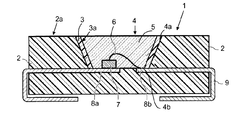
図1は、本明細書に記載されているオプトエレクトロニクスデバイスの第1の例示的な実施形態を概略的な断面図として示している。このオプトエレクトロニクスデバイスは、ハウジング1を備えている。ハウジング1は、ハウジング本体2を有する。ハウジング本体2は、第1のプラスチック材料によって形成されている。この場合、ハウジング本体2は、以下のプラスチック材料、すなわち、高温ポリアミド、ポリフェニレンサルファイド(PPS)、ポリエーテルイミド(PEI)、ポリフェニルスルホン(PPSU)、ポリエーテルケトン、LCP、のうちの少なくとも1種類を含んでいる、または少なくとも1種類からなる。リサイクルグレードの材料を使用することもできる。
FIG. 1 illustrates, as a schematic cross-sectional view, a first exemplary embodiment of the optoelectronic device described herein. The optoelectronic device includes a
ハウジング本体2には、低コスト、耐はんだ性の熱可塑性プラスチック材料を使用することが好ましい。したがって、ハウジング本体2の第1のプラスチック材料は、例えば、特に高い温度耐性を特徴とする。
The
ハウジング本体2はさらに凹部4を有し、凹部4にはハウジング本体の材料が存在しない。凹部4は、例えば、傾斜側壁4aおよび底部領域4bを境界としている。凹部4は、少なくとも1つのオプトエレクトロニクス半導体チップを受け入れる目的に適するような寸法を有する。
The
ハウジング本体2は、その上面、凹部4の底部領域4bとは反対側に、凹部4を囲んでいる外側領域2aを有する。
The
さらに、ハウジング1は、コーティング3を備えている。コーティング3は、ハウジング本体2の第1のプラスチック材料とは異なる第2のプラスチック材料によって形成されている。コーティング3には、例えば、以下の第2のプラスチック材料、すなわち、高温ポリアミド(例えば、Amodel、Grivory、Genestar、Zytel HTN、Stanyl、PA4T)(経時安定性を改善するためガラス繊維などのさらなる無機質充填材またはその他の充填材を含んでいることができる)、ポリエステル(例えば、PBT(Pocan)、PET(Impet)、PEN、PCT)(オプションとしてガラス繊維などの無機質充填材またはその他の充填材を含んでいる)、フルオロポリマー(例えばPFA、Moldflon、FEP)(オプションとしてガラス繊維などの無機質充填材またはその他の充填材を含んでいる)、PEEKもしくはLCP(オプションとしてガラス繊維などの無機質充填材またはその他の充填材を含んでいる)、液体シリコーンもしくは射出成形シリコーン、のうちの1種類、が適している。
Furthermore, the
コーティング3の外側領域3aは、例えば、電磁放射を反射する役割を果たし、この目的のため、白色顔料が含まれている。コーティング3は、例えば、第2のプラスチック材料と白色顔料とからなり、白色顔料は粒子の形をとることができる。白色顔料としては、例えば二酸化チタンを使用する。
The
白色顔料は、例えば、10%〜35%の範囲内(両端値を含む)の濃度で存在する。 The white pigment is present at a concentration within a range of 10% to 35% (including both end values), for example.
図1の例示的な実施形態においては、凹部4の領域におけるコーティング3は、ハウジング本体2の外側領域に形成されている。この場合、ハウジング本体2およびコーティング3は、2成分射出成形工程によって互いに結合されている。
In the exemplary embodiment of FIG. 1, the
さらに、ハウジング1は接続部9を有し、接続部9は、凹部4の領域において、オプトエレクトロニクス部品と電気的に接触する接続領域8a,8bを形成している。ハウジング本体2およびオプションとしてコーティング3を、多成分射出成形工程によって接続部9の一部分に結合することができる。
Further, the
さらに、このオプトエレクトロニクスデバイスは、オプトエレクトロニクス部品、例えばオプトエレクトロニクス半導体チップ7を有し、これは、放射放出オプトエレクトロニクス半導体チップ(例えば発光ダイオードチップまたはレーザダイオードチップ)であることが好ましい。
Furthermore, the optoelectronic device comprises an optoelectronic component, for example an
オプトエレクトロニクス半導体チップ7は、接続部9の第1の接続領域8aと第2の接続領域8bとに導電的に接続されている。例えば、オプトエレクトロニクス半導体チップ7を、コンタクトワイヤ6によって第2の接続領域8bに導電的に接続することができる。この場合、凹部4は注型材5によって満たされており、注型材5は放射透過性であるように形成されている。放射拡散性粒子もしくはルミネセンス変換粒子またはその両方を注型材5に含めることができる。注型材5は、例えばコーティング3の外側領域3aに直接接触している。
The
第1のプラスチック材料および第2のプラスチック材料を選択するとき、以下の組合せが特に適している。第1のプラスチック材料を最初に射出成形する場合、第1のプラスチック材料が第2のプラスチック材料よりもわずかに低い融点を有する。例えば、第1のプラスチック材料の融点は、第2のプラスチック材料の融点よりも、10°〜30°(両端値を含む)低い。第1のプラスチック材料には、例えば以下の材料、すなわち、PA4T、PA8T、PA10T/PA66、PBT、PET、のうちの1種類を使用することができる。第2のプラスチック材料には、例えば以下の材料、すなわち、PA6T/61、PA6T/66、PEEK、LCP、のうちの1種類を使用することができる。 The following combinations are particularly suitable when selecting the first plastic material and the second plastic material. When the first plastic material is first injection molded, the first plastic material has a slightly lower melting point than the second plastic material. For example, the melting point of the first plastic material is 10 ° to 30 ° (including both end values) lower than the melting point of the second plastic material. As the first plastic material, for example, one of the following materials, that is, PA4T, PA8T, PA10T / PA66, PBT, and PET can be used. As the second plastic material, for example, one of the following materials, that is, PA6T / 61, PA6T / 66, PEEK, and LCP can be used.
コーティング3の第2のプラスチック材料は、例えば、白色顔料(例えば二酸化チタンの粒子)を含んだシリコーンとすることができる。この場合、注型材5もシリコーンを含んでいる、またはシリコーンからなるならば、特に有利である。この場合、ハウジング1と注型材5との間の接着接合性が特に強く、したがって、半導体チップ7の動作時に注型材5が剥離する確率が減少する。
The second plastic material of the
本発明のオプトエレクトロニクスデバイスのさらなる例示的な実施形態について、図2の概略的な断面図を参照しながらさらに詳しく説明する。図1の例示的な実施形態との違いとして、コーティング3は、凹部4の領域においてハウジング本体2を覆っているのみならず、本体2の外側領域2aの少なくとも一部分も覆っている。例えば、コーティング3は、ハウジング本体2を、凹部4の底部領域4bとは反対側の上面において、完全に覆っている。この場合、コーティング3は、放射反射性として、もしくは放射吸収性として、またはその両方として、形成することができる。例えば、コーティング3が黒色に形成されており、したがってオプトエレクトロニクス半導体チップ7によって放出される光と周囲のハウジング1とのコントラストが特に高いならば、有利である。この場合、ハウジング本体2を異なる色(例えば白色)に形成することができる。
Further exemplary embodiments of the optoelectronic device of the present invention will be described in more detail with reference to the schematic cross-sectional view of FIG. In contrast to the exemplary embodiment of FIG. 1, the
図2の例示的な実施形態においては、コーティング3およびハウジング本体2は、この場合も2成分射出成形工程によって互いに結合されている(ハウジング本体2およびコーティング3は射出成形によって作製されている)。ハウジング本体2とコーティング3との間には結合手段が配置されておらず、ハウジングのこれら2つの構成要素の間の結合は結合手段なしで行われる。
In the exemplary embodiment of FIG. 2, the
さらなる例示的な実施形態について、図3の概略的な断面図を参照しながらさらに詳しく説明する。図1および図2の例示的な実施形態との違いとして、図3の例示的な実施形態は、さらなるコーティング30を有し、このコーティング30の光学特性は、ハウジング本体2およびコーティング3の光学特性と異なる。例えば、さらなるコーティング30は、放射吸収性として形成されているのに対して、コーティング3は反射性として形成されている。この場合、ハウジング本体2は、さらなるコーティング30よりも吸収性が低く、コーティング3よりも反射性が低いように、形成することができる。この場合、さらなるコーティング30は、さらなる射出成形工程によってハウジング本体2およびコーティング3に固定することができる。図3の例示的な実施形態においては、ハウジング1は例えば3成分射出成形工程によって製造される。
Further exemplary embodiments will be described in more detail with reference to the schematic cross-sectional view of FIG. In contrast to the exemplary embodiment of FIGS. 1 and 2, the exemplary embodiment of FIG. 3 has a
この場合、さらなるコーティング30は、ハウジング本体2の第1のプラスチック材料、コーティング3の第2のプラスチック材料、またはさらなるプラスチック材料から、形成することができる。
In this case, the
要約すると、本明細書に記載されているハウジングと、本明細書に記載されているオプトエレクトロニクスデバイスは、特に有利であり、なぜなら、ハウジング1の異なる構成要素に異なる材料が使用されており、これらの材料の特性が、それぞれの構成要素の動作要件に合うようにされているためである。したがって、凹部の領域におけるコーティング3の材料としては、電磁放射に対する高い耐性によって経年劣化に関して安定しており、かつ反射率の高い混合材料を使用することができ、ハウジング1の本体2は、例えば高い耐はんだ性(すなわち特に高い温度耐性)を特徴とする安価な(例えば再生された)プラスチックから作製される。
In summary, the housing described herein and the optoelectronic device described herein are particularly advantageous because different materials are used for different components of the
ここまで、本発明について例示的な実施形態に基づいて説明してきたが、本発明はこれらの実施形態に限定されない。本発明は、任意の新規の特徴および特徴の任意の組合せを包含しており、特に、請求項における特徴の任意の組合せを含んでいる。これらの特徴または特徴の組合せは、それ自体が請求項あるいは例示的な実施形態に明示的に記載されていない場合であっても、本発明に含まれる。 So far, the present invention has been described based on exemplary embodiments, but the present invention is not limited to these embodiments. The invention encompasses any novel feature and any combination of features, particularly any combination of features in the claims. These features or combinations of features are included in the present invention even if they are not expressly recited in the claims or in the exemplary embodiments.
本特許出願は、独国特許出願第102009055786.5号の優先権を主張し、この文書の開示内容は参照によって本出願に組み込まれている。
This patent application claims the priority of German patent application No. 10200905575786.5, the disclosure content of which is hereby incorporated by reference.
Claims (15)
− 凹部(4)を有するハウジング本体(2)と、
− 特に均一な厚さのコーティング(3)であって、少なくとも前記凹部(4)の領域において、少なくとも部分的に前記ハウジング本体(2)に結合されており、かつ前記ハウジング本体(2)に直接接触している、コーティング(3)と、
を備えており、
− 前記ハウジング本体(2)が第1のプラスチック材料から形成されており、
− 前記コーティング(3)が第2のプラスチック材料から形成されており、
− 前記第1のプラスチック材料が前記第2のプラスチック材料と異なっており、
− 前記第1のプラスチック材料と前記第2のプラスチック材料とが、以下の材料特性、すなわち、
変色に関する温度耐性、
変形に関する温度耐性、
破壊に関する温度耐性、
電磁放射に対する耐性、
のうちの少なくとも1つに関して、互いに異なる、
ハウジング。 A housing (1) for an optoelectronic component (7),
A housing body (2) having a recess (4);
A coating (3) of particularly uniform thickness, which is at least partly connected to the housing body (2) and directly to the housing body (2), at least in the region of the recess (4) The coating (3) in contact;
With
The housing body (2) is formed from a first plastic material;
The coating (3) is formed from a second plastic material;
The first plastic material is different from the second plastic material;
The first plastic material and the second plastic material have the following material properties:
Temperature tolerance for discoloration,
Temperature tolerance for deformation,
Temperature resistance for destruction,
Resistance to electromagnetic radiation,
Different from each other with respect to at least one of
housing.
請求項1に記載のハウジング。 The first plastic material is a recycled plastic material;
The housing according to claim 1.
請求項1または請求項2に記載のハウジング。 The housing body (2) and the coating (3) differ from each other in terms of their optical properties;
The housing according to claim 1 or 2.
請求項1から請求項3のいずれかに記載のハウジング。 The coating (3) has a reflectivity of 80% or more for ultraviolet radiation or visible radiation or both;
The housing according to any one of claims 1 to 3.
請求項1から請求項4のいずれかに記載のハウジング。 The coating (3) comprises the second plastic material and a white pigment;
The housing according to any one of claims 1 to 4.
二酸化チタン、リトポン、硫酸バリウム、酸化亜鉛、硫化亜鉛、アルミナ、窒化ホウ素、ジルコニア、
のうちの少なくとも1種類を含んでいる、
請求項5に記載のハウジング。 The white pigment comprises the following materials:
Titanium dioxide, lithopone, barium sulfate, zinc oxide, zinc sulfide, alumina, boron nitride, zirconia,
Including at least one of
The housing according to claim 5.
請求項1から請求項6のいずれかに記載のハウジング。 The second plastic material has a lower temperature resistance for discoloration and a higher temperature resistance for deformation than the first plastic material;
The housing according to any one of claims 1 to 6.
請求項1から請求項7のいずれかに記載のハウジング。 The first plastic material has a lower resistance to electromagnetic radiation than the second plastic material;
The housing according to any one of claims 1 to 7.
高温ポリアミド、ポリフェニレンサルファイド、ポリエーテルイミド、ポリフェニルスルホン、ポリフタルアミド、ポリエーテルエーテルケトン、LCP、PEEK
のうちの少なくとも1種類を含む群、から選択される、
請求項1から請求項8のいずれかに記載のハウジング。 The first plastic material is the following material:
High temperature polyamide, polyphenylene sulfide, polyetherimide, polyphenylsulfone, polyphthalamide, polyetheretherketone, LCP, PEEK
Selected from the group comprising at least one of
The housing according to any one of claims 1 to 8.
ポリエステル、フルオロポリマー、ポリエーテルケトン、液晶ポリマー、シリコーン、高温ポリアミド、ポリフタルアミド、
のうちの少なくとも1種類を含む群、から選択される、
請求項1から請求項9のいずれかに記載のハウジング。 The second plastic material is the following material:
Polyester, fluoropolymer, polyetherketone, liquid crystal polymer, silicone, high temperature polyamide, polyphthalamide,
Selected from the group comprising at least one of
The housing according to any one of claims 1 to 9.
を備えており、
− 前記さらなるコーティング(30)が、前記ハウジング本体の外側領域(2a)に形成されており、前記さらなるコーティング(30)が、その光学特性に関して、前記ハウジング本体および前記コーティング(3)と異なる、
請求項1から請求項10のいずれかに記載のハウジング。 A further coating (30), which is at least partially coupled to the housing body (2) and is in direct contact with the housing body (2);
With
The further coating (30) is formed in the outer region (2a) of the housing body, the further coating (30) being different from the housing body and the coating (3) in terms of its optical properties;
The housing according to any one of claims 1 to 10.
請求項1から請求項11のいずれかに記載のハウジング。 The housing body (2), the coating (3) and optionally the further coating (30) are each injection molded,
The housing according to any one of claims 1 to 11.
請求項1から請求項12のいずれかに記載のハウジング。 The housing body (2), the coating (3) and optionally the further coating (30) are mechanically coupled to each other without any coupling means;
The housing according to any one of claims 1 to 12.
− 請求項1から請求項13のいずれかに記載のハウジング(1)と、
− 少なくとも1つのオプトエレクトロニクス部品(7)、特に、放射放出半導体チップと、
を備えており、
− 前記少なくとも1つのオプトエレクトロニクス部品(7)が、前記ハウジング本体の前記凹部に配置されている、
オプトエレクトロニクスデバイス。 An optoelectronic device,
A housing (1) according to any of claims 1 to 13,
At least one optoelectronic component (7), in particular a radiation-emitting semiconductor chip;
With
The at least one optoelectronic component (7) is arranged in the recess of the housing body;
Optoelectronic devices.
14. A method of manufacturing a housing according to any of claims 1 to 13, wherein the housing body (2), the coating (3) and optionally the further coating (30) are multi-component. A method that is coupled together by an injection molding process.
Applications Claiming Priority (3)
| Application Number | Priority Date | Filing Date | Title |
|---|---|---|---|
| DE102009055786.5 | 2009-11-25 | ||
| DE102009055786A DE102009055786A1 (en) | 2009-11-25 | 2009-11-25 | Housing, optoelectronic component and method for producing a housing |
| PCT/EP2010/066650 WO2011064072A1 (en) | 2009-11-25 | 2010-11-02 | Housing for an opto-electronic component and method for producing a housing |
Publications (2)
| Publication Number | Publication Date |
|---|---|
| JP2013512556A true JP2013512556A (en) | 2013-04-11 |
| JP2013512556A5 JP2013512556A5 (en) | 2013-12-05 |
Family
ID=43383620
Family Applications (1)
| Application Number | Title | Priority Date | Filing Date |
|---|---|---|---|
| JP2012540348A Pending JP2013512556A (en) | 2009-11-25 | 2010-11-02 | Optoelectronic component housing and housing manufacturing method |
Country Status (8)
| Country | Link |
|---|---|
| US (1) | US9006773B2 (en) |
| EP (1) | EP2504861A1 (en) |
| JP (1) | JP2013512556A (en) |
| KR (1) | KR20120117792A (en) |
| CN (1) | CN102630346A (en) |
| DE (1) | DE102009055786A1 (en) |
| TW (1) | TWI440227B (en) |
| WO (1) | WO2011064072A1 (en) |
Cited By (3)
| Publication number | Priority date | Publication date | Assignee | Title |
|---|---|---|---|---|
| KR20160116270A (en) * | 2015-03-27 | 2016-10-07 | 삼성디스플레이 주식회사 | Light emitting diode package |
| JP2017152629A (en) * | 2016-02-26 | 2017-08-31 | 日亜化学工業株式会社 | Light-emitting device and illuminating apparatus using the same |
| US10879425B2 (en) | 2018-06-21 | 2020-12-29 | Nichia Corporation | Light-emitting device |
Families Citing this family (13)
| Publication number | Priority date | Publication date | Assignee | Title |
|---|---|---|---|---|
| DE102010013317B4 (en) * | 2010-03-30 | 2021-07-22 | OSRAM Opto Semiconductors Gesellschaft mit beschränkter Haftung | Optoelectronic component, housing therefor and method for producing the optoelectronic component |
| CN203260631U (en) * | 2010-07-01 | 2013-10-30 | 西铁城控股株式会社 | Led light source device |
| JP2014011029A (en) * | 2012-06-29 | 2014-01-20 | Toshiba Lighting & Technology Corp | Lighting apparatus |
| WO2013025832A1 (en) * | 2011-08-16 | 2013-02-21 | E. I. Du Pont De Nemours And Company | Reflector for light-emitting diode and housing |
| JP2013222499A (en) * | 2012-04-12 | 2013-10-28 | Sharp Corp | Light source substrate unit |
| CN102779926B (en) * | 2012-08-02 | 2015-01-28 | 慧明光电(深圳)有限公司 | Waterproof watch patch LED (light emitting diode) lamp with high-contract ratio |
| DE102014102258B4 (en) * | 2014-02-21 | 2021-08-05 | OSRAM Opto Semiconductors Gesellschaft mit beschränkter Haftung | Optoelectronic component |
| DE102014106882A1 (en) * | 2014-05-15 | 2015-11-19 | Osram Opto Semiconductors Gmbh | Optoelectronic component |
| US10256383B2 (en) * | 2015-06-01 | 2019-04-09 | Mitsubishi Electric Corporation | Light emitting device with dark area and greater reflectance light area, display unit, and image display device |
| JP7117170B2 (en) * | 2018-06-20 | 2022-08-12 | スタンレー電気株式会社 | light emitting device |
| JP7190889B2 (en) * | 2018-12-07 | 2022-12-16 | スタンレー電気株式会社 | Light-emitting device and light-emitting device module |
| TWI740149B (en) * | 2019-05-24 | 2021-09-21 | 華碩電腦股份有限公司 | Manufacturing method of housing |
| CN113410374B (en) * | 2021-06-17 | 2022-10-04 | 中国科学院半导体研究所 | Mixed-color LED device |
Citations (10)
| Publication number | Priority date | Publication date | Assignee | Title |
|---|---|---|---|---|
| JPH07195580A (en) * | 1993-12-14 | 1995-08-01 | Ems Inventa Ag | Molded article having support core part and protective layer surrounding it |
| JP2000037726A (en) * | 1998-07-21 | 2000-02-08 | Toray Ind Inc | Method for recycling thermoplastic resin products |
| JP2004071950A (en) * | 2002-08-08 | 2004-03-04 | Matsushita Electric Ind Co Ltd | Semiconductor package and manufacturing method thereof |
| JP2006108640A (en) * | 2004-09-09 | 2006-04-20 | Toyoda Gosei Co Ltd | Light emitting device |
| JP2007042668A (en) * | 2005-07-29 | 2007-02-15 | Toyoda Gosei Co Ltd | Led light emitting device |
| JP2007262259A (en) * | 2006-03-29 | 2007-10-11 | Toray Ind Inc | Recycling polyamide resin composition |
| JP2007281260A (en) * | 2006-04-07 | 2007-10-25 | Sumitomo Metal Electronics Devices Inc | Reflector, package for housing light-emitting element using the same, and lens used for reflector |
| JP2008060344A (en) * | 2006-08-31 | 2008-03-13 | Toshiba Corp | Semiconductor light-emitting device |
| WO2008040324A1 (en) * | 2006-09-29 | 2008-04-10 | Osram Opto Semiconductors Gmbh | Housing for an optoelectronic component, optoelectronic component and method for producing a housing for an optoelectronic component |
| WO2008125096A2 (en) * | 2007-04-16 | 2008-10-23 | Osram Opto Semiconductors Gmbh | Method for producing an opto-electronic component and opto-electronic component |
Family Cites Families (14)
| Publication number | Priority date | Publication date | Assignee | Title |
|---|---|---|---|---|
| DE10020465A1 (en) * | 2000-04-26 | 2001-11-08 | Osram Opto Semiconductors Gmbh | Radiation-emitting semiconductor component with luminescence conversion element |
| JP2002374007A (en) | 2001-06-15 | 2002-12-26 | Toyoda Gosei Co Ltd | Light-emitting apparatus |
| DE10153259A1 (en) * | 2001-10-31 | 2003-05-22 | Osram Opto Semiconductors Gmbh | Optoelectronic component |
| US20030133300A1 (en) * | 2002-01-11 | 2003-07-17 | Bily Wang | Light absorbing wall for LED package |
| DE10229067B4 (en) | 2002-06-28 | 2007-08-16 | Osram Opto Semiconductors Gmbh | Optoelectronic component and method for its production |
| US7718451B2 (en) | 2003-02-28 | 2010-05-18 | Osram Opto Semiconductor Gmbh | Method for producing an optoelectronic device with patterned-metallized package body and method for the patterned metalization of a plastic-containing body |
| DE102004031391B4 (en) | 2004-06-29 | 2009-06-04 | Osram Opto Semiconductors Gmbh | Electronic component with housing for ESD protection |
| DE102005036520A1 (en) | 2005-04-26 | 2006-11-09 | Osram Opto Semiconductors Gmbh | Optical component, optoelectronic component with the component and its manufacture |
| US8044412B2 (en) * | 2006-01-20 | 2011-10-25 | Taiwan Semiconductor Manufacturing Company, Ltd | Package for a light emitting element |
| JP4846498B2 (en) | 2006-09-22 | 2011-12-28 | 株式会社東芝 | Optical semiconductor device and method for manufacturing optical semiconductor device |
| CN101578711A (en) | 2006-11-09 | 2009-11-11 | 跃进封装公司 | Leg reflective package |
| US7956469B2 (en) * | 2007-07-27 | 2011-06-07 | Nichia Corporation | Light emitting device and method of manufacturing the same |
| WO2009075530A2 (en) * | 2007-12-13 | 2009-06-18 | Amoleds Co., Ltd. | Semiconductor and manufacturing method thereof |
| DE102008038748B4 (en) | 2008-08-12 | 2022-08-04 | OSRAM Opto Semiconductors Gesellschaft mit beschränkter Haftung | Surface-mount optoelectronic semiconductor component |
-
2009
- 2009-11-25 DE DE102009055786A patent/DE102009055786A1/en not_active Withdrawn
-
2010
- 2010-11-02 WO PCT/EP2010/066650 patent/WO2011064072A1/en active Application Filing
- 2010-11-02 CN CN201080053529XA patent/CN102630346A/en active Pending
- 2010-11-02 JP JP2012540348A patent/JP2013512556A/en active Pending
- 2010-11-02 US US13/511,414 patent/US9006773B2/en not_active Expired - Fee Related
- 2010-11-02 EP EP10773316A patent/EP2504861A1/en not_active Withdrawn
- 2010-11-02 KR KR1020127016558A patent/KR20120117792A/en not_active Application Discontinuation
- 2010-11-22 TW TW099140164A patent/TWI440227B/en not_active IP Right Cessation
Patent Citations (10)
| Publication number | Priority date | Publication date | Assignee | Title |
|---|---|---|---|---|
| JPH07195580A (en) * | 1993-12-14 | 1995-08-01 | Ems Inventa Ag | Molded article having support core part and protective layer surrounding it |
| JP2000037726A (en) * | 1998-07-21 | 2000-02-08 | Toray Ind Inc | Method for recycling thermoplastic resin products |
| JP2004071950A (en) * | 2002-08-08 | 2004-03-04 | Matsushita Electric Ind Co Ltd | Semiconductor package and manufacturing method thereof |
| JP2006108640A (en) * | 2004-09-09 | 2006-04-20 | Toyoda Gosei Co Ltd | Light emitting device |
| JP2007042668A (en) * | 2005-07-29 | 2007-02-15 | Toyoda Gosei Co Ltd | Led light emitting device |
| JP2007262259A (en) * | 2006-03-29 | 2007-10-11 | Toray Ind Inc | Recycling polyamide resin composition |
| JP2007281260A (en) * | 2006-04-07 | 2007-10-25 | Sumitomo Metal Electronics Devices Inc | Reflector, package for housing light-emitting element using the same, and lens used for reflector |
| JP2008060344A (en) * | 2006-08-31 | 2008-03-13 | Toshiba Corp | Semiconductor light-emitting device |
| WO2008040324A1 (en) * | 2006-09-29 | 2008-04-10 | Osram Opto Semiconductors Gmbh | Housing for an optoelectronic component, optoelectronic component and method for producing a housing for an optoelectronic component |
| WO2008125096A2 (en) * | 2007-04-16 | 2008-10-23 | Osram Opto Semiconductors Gmbh | Method for producing an opto-electronic component and opto-electronic component |
Cited By (4)
| Publication number | Priority date | Publication date | Assignee | Title |
|---|---|---|---|---|
| KR20160116270A (en) * | 2015-03-27 | 2016-10-07 | 삼성디스플레이 주식회사 | Light emitting diode package |
| KR102360957B1 (en) * | 2015-03-27 | 2022-02-11 | 삼성디스플레이 주식회사 | Light emitting diode package |
| JP2017152629A (en) * | 2016-02-26 | 2017-08-31 | 日亜化学工業株式会社 | Light-emitting device and illuminating apparatus using the same |
| US10879425B2 (en) | 2018-06-21 | 2020-12-29 | Nichia Corporation | Light-emitting device |
Also Published As
| Publication number | Publication date |
|---|---|
| TWI440227B (en) | 2014-06-01 |
| US20120273811A1 (en) | 2012-11-01 |
| CN102630346A (en) | 2012-08-08 |
| US9006773B2 (en) | 2015-04-14 |
| KR20120117792A (en) | 2012-10-24 |
| DE102009055786A1 (en) | 2011-05-26 |
| EP2504861A1 (en) | 2012-10-03 |
| WO2011064072A1 (en) | 2011-06-03 |
| TW201131826A (en) | 2011-09-16 |
Similar Documents
| Publication | Publication Date | Title |
|---|---|---|
| JP2013512556A (en) | Optoelectronic component housing and housing manufacturing method | |
| JP5340157B2 (en) | Housing for optoelectronic devices, optoelectronic device, and method of manufacturing housing for optoelectronic devices | |
| US9331255B2 (en) | Housing that includes reflector part and housing material formed with plastic material | |
| KR100927077B1 (en) | Optical semiconductor device and manufacturing method thereof | |
| JP4709487B2 (en) | Optoelectronic devices | |
| KR101007131B1 (en) | Light emitting device package | |
| US8569782B2 (en) | Optoelectronic semiconductor component | |
| KR20060132298A (en) | Light emitting device package | |
| US20080197368A1 (en) | Optoelectronic Component and Package For an Optoelectronic Component | |
| KR101772722B1 (en) | Optoelectronic component | |
| WO2011033404A1 (en) | Reduced angular emission cone illumination leds | |
| TWI435469B (en) | Cover for optoelectronic components | |
| JP6361645B2 (en) | Light emitting device | |
| KR20190023046A (en) | Semiconductor package structure | |
| JP2012533182A (en) | Light emitting diode and method for manufacturing light emitting diode | |
| JP2012533182A5 (en) | ||
| JP7196577B2 (en) | Vehicle lighting device and vehicle lamp | |
| CN102244179B (en) | Encapsulation structure for light-emitting diode and manufacturing method thereof | |
| JP2007311674A (en) | Semiconductor light-emitting device | |
| US10937933B2 (en) | Light-emitting component and method of producing a light-emitting component | |
| KR101797968B1 (en) | Light Emitting Device Package | |
| KR20100002665A (en) | Light emitting diode package | |
| KR20090132087A (en) | Led package |
Legal Events
| Date | Code | Title | Description |
|---|---|---|---|
| A521 | Request for written amendment filed |
Free format text: JAPANESE INTERMEDIATE CODE: A523 Effective date: 20131018 |
|
| A621 | Written request for application examination |
Free format text: JAPANESE INTERMEDIATE CODE: A621 Effective date: 20131018 |
|
| A977 | Report on retrieval |
Free format text: JAPANESE INTERMEDIATE CODE: A971007 Effective date: 20140327 |
|
| A131 | Notification of reasons for refusal |
Free format text: JAPANESE INTERMEDIATE CODE: A131 Effective date: 20140401 |
|
| A601 | Written request for extension of time |
Free format text: JAPANESE INTERMEDIATE CODE: A601 Effective date: 20140613 |
|
| A602 | Written permission of extension of time |
Free format text: JAPANESE INTERMEDIATE CODE: A602 Effective date: 20140620 |
|
| A521 | Request for written amendment filed |
Free format text: JAPANESE INTERMEDIATE CODE: A523 Effective date: 20140930 |
|
| A131 | Notification of reasons for refusal |
Free format text: JAPANESE INTERMEDIATE CODE: A131 Effective date: 20141216 |
|
| A601 | Written request for extension of time |
Free format text: JAPANESE INTERMEDIATE CODE: A601 Effective date: 20150220 |
|
| A521 | Request for written amendment filed |
Free format text: JAPANESE INTERMEDIATE CODE: A523 Effective date: 20150611 |
|
| A131 | Notification of reasons for refusal |
Free format text: JAPANESE INTERMEDIATE CODE: A131 Effective date: 20150804 |
|
| A02 | Decision of refusal |
Free format text: JAPANESE INTERMEDIATE CODE: A02 Effective date: 20160105 |