JP2013257593A - Mask blank, method of manufacturing the same, and transfer mask - Google Patents
Mask blank, method of manufacturing the same, and transfer mask Download PDFInfo
- Publication number
- JP2013257593A JP2013257593A JP2013177415A JP2013177415A JP2013257593A JP 2013257593 A JP2013257593 A JP 2013257593A JP 2013177415 A JP2013177415 A JP 2013177415A JP 2013177415 A JP2013177415 A JP 2013177415A JP 2013257593 A JP2013257593 A JP 2013257593A
- Authority
- JP
- Japan
- Prior art keywords
- film
- mask blank
- mask
- thin film
- pattern
- Prior art date
- Legal status (The legal status is an assumption and is not a legal conclusion. Google has not performed a legal analysis and makes no representation as to the accuracy of the status listed.)
- Granted
Links
Images


Classifications
-
- G—PHYSICS
- G03—PHOTOGRAPHY; CINEMATOGRAPHY; ANALOGOUS TECHNIQUES USING WAVES OTHER THAN OPTICAL WAVES; ELECTROGRAPHY; HOLOGRAPHY
- G03F—PHOTOMECHANICAL PRODUCTION OF TEXTURED OR PATTERNED SURFACES, e.g. FOR PRINTING, FOR PROCESSING OF SEMICONDUCTOR DEVICES; MATERIALS THEREFOR; ORIGINALS THEREFOR; APPARATUS SPECIALLY ADAPTED THEREFOR
- G03F1/00—Originals for photomechanical production of textured or patterned surfaces, e.g., masks, photo-masks, reticles; Mask blanks or pellicles therefor; Containers specially adapted therefor; Preparation thereof
- G03F1/50—Mask blanks not covered by G03F1/20 - G03F1/34; Preparation thereof
-
- G—PHYSICS
- G03—PHOTOGRAPHY; CINEMATOGRAPHY; ANALOGOUS TECHNIQUES USING WAVES OTHER THAN OPTICAL WAVES; ELECTROGRAPHY; HOLOGRAPHY
- G03F—PHOTOMECHANICAL PRODUCTION OF TEXTURED OR PATTERNED SURFACES, e.g. FOR PRINTING, FOR PROCESSING OF SEMICONDUCTOR DEVICES; MATERIALS THEREFOR; ORIGINALS THEREFOR; APPARATUS SPECIALLY ADAPTED THEREFOR
- G03F1/00—Originals for photomechanical production of textured or patterned surfaces, e.g., masks, photo-masks, reticles; Mask blanks or pellicles therefor; Containers specially adapted therefor; Preparation thereof
- G03F1/54—Absorbers, e.g. of opaque materials
-
- G—PHYSICS
- G03—PHOTOGRAPHY; CINEMATOGRAPHY; ANALOGOUS TECHNIQUES USING WAVES OTHER THAN OPTICAL WAVES; ELECTROGRAPHY; HOLOGRAPHY
- G03F—PHOTOMECHANICAL PRODUCTION OF TEXTURED OR PATTERNED SURFACES, e.g. FOR PRINTING, FOR PROCESSING OF SEMICONDUCTOR DEVICES; MATERIALS THEREFOR; ORIGINALS THEREFOR; APPARATUS SPECIALLY ADAPTED THEREFOR
- G03F1/00—Originals for photomechanical production of textured or patterned surfaces, e.g., masks, photo-masks, reticles; Mask blanks or pellicles therefor; Containers specially adapted therefor; Preparation thereof
- G03F1/38—Masks having auxiliary features, e.g. special coatings or marks for alignment or testing; Preparation thereof
-
- G—PHYSICS
- G03—PHOTOGRAPHY; CINEMATOGRAPHY; ANALOGOUS TECHNIQUES USING WAVES OTHER THAN OPTICAL WAVES; ELECTROGRAPHY; HOLOGRAPHY
- G03F—PHOTOMECHANICAL PRODUCTION OF TEXTURED OR PATTERNED SURFACES, e.g. FOR PRINTING, FOR PROCESSING OF SEMICONDUCTOR DEVICES; MATERIALS THEREFOR; ORIGINALS THEREFOR; APPARATUS SPECIALLY ADAPTED THEREFOR
- G03F1/00—Originals for photomechanical production of textured or patterned surfaces, e.g., masks, photo-masks, reticles; Mask blanks or pellicles therefor; Containers specially adapted therefor; Preparation thereof
- G03F1/60—Substrates
-
- G—PHYSICS
- G03—PHOTOGRAPHY; CINEMATOGRAPHY; ANALOGOUS TECHNIQUES USING WAVES OTHER THAN OPTICAL WAVES; ELECTROGRAPHY; HOLOGRAPHY
- G03F—PHOTOMECHANICAL PRODUCTION OF TEXTURED OR PATTERNED SURFACES, e.g. FOR PRINTING, FOR PROCESSING OF SEMICONDUCTOR DEVICES; MATERIALS THEREFOR; ORIGINALS THEREFOR; APPARATUS SPECIALLY ADAPTED THEREFOR
- G03F7/00—Photomechanical, e.g. photolithographic, production of textured or patterned surfaces, e.g. printing surfaces; Materials therefor, e.g. comprising photoresists; Apparatus specially adapted therefor
- G03F7/70—Microphotolithographic exposure; Apparatus therefor
- G03F7/70216—Mask projection systems
-
- G—PHYSICS
- G03—PHOTOGRAPHY; CINEMATOGRAPHY; ANALOGOUS TECHNIQUES USING WAVES OTHER THAN OPTICAL WAVES; ELECTROGRAPHY; HOLOGRAPHY
- G03F—PHOTOMECHANICAL PRODUCTION OF TEXTURED OR PATTERNED SURFACES, e.g. FOR PRINTING, FOR PROCESSING OF SEMICONDUCTOR DEVICES; MATERIALS THEREFOR; ORIGINALS THEREFOR; APPARATUS SPECIALLY ADAPTED THEREFOR
- G03F7/00—Photomechanical, e.g. photolithographic, production of textured or patterned surfaces, e.g. printing surfaces; Materials therefor, e.g. comprising photoresists; Apparatus specially adapted therefor
- G03F7/70—Microphotolithographic exposure; Apparatus therefor
- G03F7/70691—Handling of masks or workpieces
-
- H—ELECTRICITY
- H01—ELECTRIC ELEMENTS
- H01L—SEMICONDUCTOR DEVICES NOT COVERED BY CLASS H10
- H01L21/00—Processes or apparatus adapted for the manufacture or treatment of semiconductor or solid state devices or of parts thereof
- H01L21/02—Manufacture or treatment of semiconductor devices or of parts thereof
- H01L21/027—Making masks on semiconductor bodies for further photolithographic processing not provided for in group H01L21/18 or H01L21/34
- H01L21/0271—Making masks on semiconductor bodies for further photolithographic processing not provided for in group H01L21/18 or H01L21/34 comprising organic layers
- H01L21/0273—Making masks on semiconductor bodies for further photolithographic processing not provided for in group H01L21/18 or H01L21/34 comprising organic layers characterised by the treatment of photoresist layers
- H01L21/0274—Photolithographic processes
Abstract
Description
本発明は、半導体装置等の電子デバイスの製造において使用されるフォトマスク(転写用マスク)を作製するために用いるマスクブランク及びその製造方法並びに転写用マスクに関する。 The present invention relates to a mask blank used for manufacturing a photomask (transfer mask) used in manufacturing an electronic device such as a semiconductor device, a manufacturing method thereof, and a transfer mask.
一般に、半導体装置の製造工程では、フォトリソグラフィー法を用いて微細パターンの形成が行われている。また、この微細パターンの形成には通常何枚ものフォトマスク(以下、転写用マスクと呼ぶ。)と呼ばれている基板が使用される。この転写用マスクは、一般に透光性のガラス基板上に、金属薄膜等からなる微細パターンを設けたものであり、この転写用マスクの製造においてもフォトリソグラフィー法が用いられている。 In general, in a manufacturing process of a semiconductor device, a fine pattern is formed using a photolithography method. In order to form this fine pattern, a number of substrates called photomasks (hereinafter referred to as transfer masks) are usually used. This transfer mask is generally provided with a fine pattern made of a metal thin film on a translucent glass substrate, and the photolithographic method is also used in the production of this transfer mask.
フォトリソグラフィー法による転写用マスクの製造には、ガラス基板等の透光性基板上に転写パターン(マスクパターン)を形成するための薄膜(例えば遮光膜など)を有するマスクブランクが用いられる。このマスクブランクを用いた転写用マスクの製造は、マスクブランク上に形成されたレジスト膜に対し、所望のパターン描画を施す露光工程と、所望のパターン描画に従って前記レジスト膜を現像してレジストパターンを形成する現像工程と、レジストパターンに従って前記薄膜をエッチングするエッチング工程と、残存したレジストパターンを剥離除去する工程とを有して行われている。上記現像工程では、マスクブランク上に形成されたレジスト膜に対し所望のパターン描画を施した後に現像液を供給して、現像液に可溶なレジスト膜の部位を溶解し、レジストパターンを形成する。また、上記エッチング工程では、このレジストパターンをマスクとして、ドライエッチング又はウェットエッチングによって、レジストパターンの形成されていない薄膜が露出した部位を溶解し、これにより所望のマスクパターンを透光性基板上に形成する。こうして、転写用マスクが出来上がる。 In manufacturing a transfer mask by photolithography, a mask blank having a thin film (for example, a light shielding film) for forming a transfer pattern (mask pattern) on a light-transmitting substrate such as a glass substrate is used. In the manufacture of a transfer mask using this mask blank, an exposure process for drawing a desired pattern on the resist film formed on the mask blank, and developing the resist film in accordance with the desired pattern drawing, the resist pattern is developed. The development step is formed, the etching step is to etch the thin film in accordance with the resist pattern, and the step is to remove and remove the remaining resist pattern. In the developing step, a desired pattern is drawn on the resist film formed on the mask blank, and then a developing solution is supplied to dissolve a portion of the resist film that is soluble in the developing solution, thereby forming a resist pattern. . In the etching step, the resist pattern is used as a mask to dissolve the exposed portion of the thin film on which the resist pattern is not formed by dry etching or wet etching, thereby forming a desired mask pattern on the light-transmitting substrate. Form. Thus, a transfer mask is completed.
半導体装置のパターンを微細化するに当たっては、転写用マスクに形成されるマスクパターンの微細化に加え、フォトリソグラフィーで使用される露光光源波長の短波長化が必要となる。半導体装置製造の際の露光光源としては、近年ではKrFエキシマレーザー(波長248nm)から、ArFエキシマレーザー(波長193nm)、さらにEUV(波長13.4nm)へと短波長化が進んでいる。 When miniaturizing a pattern of a semiconductor device, it is necessary to shorten the wavelength of an exposure light source used in photolithography in addition to miniaturization of a mask pattern formed on a transfer mask. As an exposure light source for manufacturing a semiconductor device, in recent years, the wavelength has been shortened from a KrF excimer laser (wavelength 248 nm) to an ArF excimer laser (wavelength 193 nm) and further to EUV (wavelength 13.4 nm).
また、転写用マスクの種類としては、従来の透光性基板上にクロム系材料などからなる遮光膜パターンを有するバイナリマスクのほかに、ハーフトーン型位相シフトマスクが知られている。このハーフトーン型位相シフトマスクは、透光性基板上に位相シフト膜を有する構造のもので、この位相シフト膜は、実質的に露光に寄与しない強度の光(例えば、露光波長に対して1%〜30%)を透過させ、所定の位相差を有するものであり、例えばモリブデンシリサイド化合物を含む材料等が用いられる。このハーフトーン型位相シフトマスクは、位相シフト膜をパターニングした光半透過部と、位相シフト膜が形成されていない実質的に露光に寄与する強度の光を透過させる光透過部とによって、光半透過部を透過して光の位相が光透過部を透過した光の位相に対して実質的に反転した関係になるようにすることによって、光半透過部と光透過部との境界部近傍を通過し回折現象によって互いに相手の領域に回りこんだ光が互いに打ち消しあうようにし、境界部における光強度をほぼゼロとし境界部のコントラスト即ち解像度を向上させるものである。
また、近年では、モリブデンシリサイド化合物を含む材料を遮光膜として用いたArFエキシマレーザー用のバイナリマスクブランクなども出現している。
As a type of transfer mask, a halftone phase shift mask is known in addition to a binary mask having a light-shielding film pattern made of a chromium-based material or the like on a conventional translucent substrate. This halftone type phase shift mask has a structure having a phase shift film on a translucent substrate, and this phase shift film has a light intensity that does not substantially contribute to exposure (for example, 1 for the exposure wavelength). % To 30%) and has a predetermined phase difference. For example, a material containing a molybdenum silicide compound is used. This halftone phase shift mask has a light semi-transmission part patterned with a phase shift film and a light semi-transmission part that does not have a phase shift film and transmits light having a strength that substantially contributes to exposure. By making the phase of the light transmitted through the transmission part substantially inverted with respect to the phase of the light transmitted through the light transmission part, the vicinity of the boundary between the light semi-transmission part and the light transmission part is The light that has passed through and diffracted to each other by the diffraction phenomenon cancels each other, and the light intensity at the boundary is made almost zero to improve the contrast of the boundary, that is, the resolution.
In recent years, binary mask blanks for ArF excimer lasers using a material containing a molybdenum silicide compound as a light shielding film have also appeared.
転写用マスクに形成されるマスクパターンを微細化するに当たっては、マスクブランクにおけるレジスト膜の薄膜化と、転写用マスク製造の際のパターニング手法として、ドライエッチング加工が必要である。 In order to miniaturize the mask pattern formed on the transfer mask, a dry etching process is required as a thinning of the resist film in the mask blank and as a patterning technique for manufacturing the transfer mask.
しかし、レジスト膜の薄膜化とドライエッチング加工は、以下に示す技術的な問題が生じている。
一つは、マスクブランクのレジスト膜の薄膜化を進める際、例えば遮光膜の加工時間が1つの大きな制限事項となっていることである。遮光膜の材料として例えばクロムを用いる場合、クロムのドライエッチング加工では、エッチングガスに塩素ガスと酸素ガスの混合ガスが用いられている。レジストパターンをマスクにして遮光膜をドライエッチングでパターニングする際、レジストは有機膜でありその主成分は炭素であるので、ドライエッチング環境である酸素プラズマに対しては非常に弱い。遮光膜をドライエッチングでパターニングする間、その遮光膜上に形成されているレジストパターンは十分な膜厚で残っていなければならない。一つの指標として、マスクパターンの断面形状を良好にするために、ジャストエッチングタイムの2倍(100%オーバーエッチング)程度を行っても残存するようなレジスト膜厚にしなければならない。例えば、一般には、遮光膜の材料であるクロムと、レジスト膜とのエッチング選択比は1以下となっているので、レジスト膜の膜厚は、遮光膜の膜厚の2倍以上の膜厚が必要となることになる。従って、レジスト膜を薄膜化するためには、遮光膜の加工時間を短くする必要があるが、そのためには遮光膜の薄膜化が重要な課題である。しかし、遮光膜を薄膜化するといっても、遮光性を確保するためには所定の光学濃度(通常、マスクを使用する露光光の波長において3.0以上)が必要であり、遮光膜の薄膜化には自ずと限界がある。
However, the thinning of the resist film and the dry etching process have the following technical problems.
One is that when the resist film of the mask blank is made thinner, for example, the processing time of the light shielding film is one big limitation. When chromium is used as the material of the light shielding film, for example, in the dry etching of chromium, a mixed gas of chlorine gas and oxygen gas is used as an etching gas. When the light-shielding film is patterned by dry etching using the resist pattern as a mask, the resist is an organic film and its main component is carbon, so it is very weak against oxygen plasma which is a dry etching environment. While the light shielding film is patterned by dry etching, the resist pattern formed on the light shielding film must remain with a sufficient thickness. As one index, in order to improve the cross-sectional shape of the mask pattern, the resist film thickness must remain so as to remain even if it is performed about twice the just etching time (100% overetching). For example, in general, the etching selection ratio between chromium, which is a material of the light shielding film, and the resist film is 1 or less, so the film thickness of the resist film is more than twice the film thickness of the light shielding film. It will be necessary. Therefore, in order to reduce the thickness of the resist film, it is necessary to shorten the processing time of the light shielding film. To that end, it is an important issue to reduce the thickness of the light shielding film. However, even if the light-shielding film is thinned, a predetermined optical density (usually 3.0 or more at the wavelength of exposure light using a mask) is necessary to ensure light-shielding properties. Naturalization has its own limits.
そこで、レジスト膜の膜厚を薄膜化する方法として、従来は、遮光膜の上に、遮光膜とはエッチング選択性のある材料で形成されるエッチングマスク膜を設け、まず、レジストパターンをマスクとして、上記エッチングマスク膜をエッチングして、エッチングマスク膜パターンを形成し、次いで、このエッチングマスク膜パターンをマスクとして、上記遮光膜をエッチングして、遮光膜パターンを形成する方法が提案されている(例えば特許文献1等)。 Therefore, as a method of reducing the thickness of the resist film, conventionally, an etching mask film formed of a material having an etching selectivity with respect to the light shielding film is provided on the light shielding film, and the resist pattern is used as a mask first. The etching mask film is etched to form an etching mask film pattern, and then the light shielding film is etched using the etching mask film pattern as a mask to form a light shielding film pattern ( For example, Patent Document 1).
ところで、レジスト膜にレジストパターンを形成する場合、レジストパターンの線幅がレジスト膜厚の1/3よりも小さくなると、レジストパターンの倒れや欠けなどが発生するため、レジストも膜厚はそれ以下にする必要がある。DRAMハーフピッチ32nmの世代では、これらの点を考慮すると、レジスト膜厚は180nm以下とする必要があり、さらにDRAMハーフピッチ22nmの世代では、レジスト膜厚は100nm以下とする必要がある。しかし、上述したように、マスクブランクのレジスト膜を薄膜化するには、上述のエッチングマスク膜を設けるにしても、例えば遮光膜(またはエッチングマスク膜)の加工時間が1つの大きな制限事項となっているため、単にレジスト膜の薄膜化だけを達成するのは困難である。 By the way, when forming a resist pattern on the resist film, if the line width of the resist pattern is smaller than 1/3 of the resist film thickness, the resist pattern may fall down or chip, and the resist film thickness is less than that. There is a need to. In consideration of these points, the generation of the DRAM half pitch of 32 nm requires the resist film thickness to be 180 nm or less, and the generation of the DRAM half pitch of 22 nm requires the resist film thickness to be 100 nm or less. However, as described above, in order to reduce the thickness of the resist film of the mask blank, even if the above-described etching mask film is provided, for example, the processing time of the light shielding film (or etching mask film) is one major limitation. Therefore, it is difficult to simply reduce the thickness of the resist film.
また、マスクブランクのパターン形成用薄膜(例えば遮光膜)のレジストとの密着性が悪いと、上述のレジストパターンの倒れや欠けなどの問題はいっそう顕著になる。例えば、ケイ素の酸窒化物やそれに遷移金属を含有させた材料の場合、レジストに対する密着性がクロム系の材料に比べて低く、形成されるレジストパターンの線幅に対するレジスト膜厚が1/3未満であっても、レジストパターンの倒れや欠けが発生し易い。また、近年、レジストとして、解像性の高い化学増幅型レジストが用いられることが多くなってきているが、この化学増幅型レジストの場合、クロム系の材料においても、レジストに対する密着性が不十分である。
転写用マスクに形成されるマスクパターンの微細化の要求は益々厳しくなるばかりであるが、マスクパターンのよりいっそうの微細化を実現する上で、マスクブランクにおけるレジストとの密着性の向上は重要な課題となっている。
Further, when the adhesion of the mask blank pattern forming thin film (for example, a light-shielding film) to the resist is poor, problems such as the above-described collapse or chipping of the resist pattern become more remarkable. For example, in the case of a material containing silicon oxynitride or a transition metal, the adhesion to the resist is lower than that of a chromium-based material, and the resist film thickness with respect to the line width of the formed resist pattern is less than 1/3. Even so, the resist pattern is liable to fall or chip. In recent years, a chemically amplified resist having high resolution has been increasingly used as a resist. However, in the case of this chemically amplified resist, even a chromium-based material has insufficient adhesion to the resist. It is.
The demand for miniaturization of the mask pattern formed on the transfer mask is becoming increasingly severe, but in order to realize further miniaturization of the mask pattern, it is important to improve the adhesion of the mask blank to the resist. It has become a challenge.
そこで本発明は、従来の課題を解決するべくなされたものであり、その目的とするところは、転写パターンを形成するための薄膜の表面改質を行うことでレジストに対する密着性を向上させ、形成されたレジストパターンの倒れや欠けなどの発生を抑制できるマスクブランク及びその製造方法並びに転写用マスクを提供することである。 Therefore, the present invention has been made to solve the conventional problems, and the object of the present invention is to improve the adhesion to a resist by modifying the surface of a thin film for forming a transfer pattern. It is to provide a mask blank, a manufacturing method thereof, and a transfer mask that can suppress the occurrence of falling or chipping of the resist pattern.
本発明者は、上記課題を解決するため鋭意研究した結果、転写パターンを形成するための金属を含む材料からなる薄膜を有するマスクブランクにおいて、薄膜の表面に炭化水素を含む酸化膜からなる表面改質層を形成することにより、薄膜の光学特性や表面粗さなどを劣化させることなく、レジストに対する密着性を向上できることを見い出した。またさらに、このような薄膜の光学特性や表面粗さなどを劣化させることなく、薄膜の表面に炭化水素を含む酸化膜を形成するためには、薄膜の表面に対して高濃度オゾンガスと不飽和炭化水素ガスの混合ガスを作用させる処理が最適であることも見い出した。
本発明者は以上の解明事実に基づき、さらに鋭意検討を続けた結果、本発明を完成したものである。
すなわち、上記課題を解決するため、本発明は以下の構成を有する。
As a result of diligent research to solve the above problems, the present inventor has found that in a mask blank having a thin film made of a material containing a metal for forming a transfer pattern, a surface modification made of an oxide film containing hydrocarbon on the surface of the thin film. It has been found that the adhesion to the resist can be improved without degrading the optical properties and surface roughness of the thin film by forming the quality layer. Furthermore, in order to form an oxide film containing hydrocarbons on the surface of the thin film without degrading the optical properties and surface roughness of the thin film, high-concentration ozone gas and unsaturation are formed on the surface of the thin film. It has also been found that a treatment using a mixed gas of hydrocarbon gas is optimal.
The present inventor has completed the present invention as a result of further intensive studies based on the above elucidated facts.
That is, in order to solve the above problems, the present invention has the following configuration.
(構成1)
基板上に、転写パターンを形成するための金属を含む材料からなる薄膜を有するマスクブランクであって、前記薄膜は、炭化水素を含む酸化膜からなる表面改質層を有することを特徴とするマスクブランクである。
(構成2)
前記薄膜は積層膜であり、該積層膜の最上層は前記金属として遷移金属を含む材料からなることを特徴とする構成1に記載のマスクブランクである。
(構成3)
前記遷移金属は、クロムであり、前記表面改質層は、X線光電子分光法(XPS)によって測定されるO(酸素)1sスペクトルにおいて、結合エネルギーがそれぞれ532eV付近にある第1のピークと530eV付近にある第2のピークとに分離したときに、第2のピーク面積に対する第1のピーク面積の割合が2.0以上であることを特徴とする構成2に記載のマスクブランクである。
(Configuration 1)
A mask blank having a thin film made of a material containing a metal for forming a transfer pattern on a substrate, wherein the thin film has a surface modification layer made of an oxide film containing a hydrocarbon. It is blank.
(Configuration 2)
2. The mask blank according to
(Configuration 3)
The transition metal is chromium, and the surface modification layer has a first peak of 530 eV and a binding energy of about 532 eV in the O (oxygen) 1s spectrum measured by X-ray photoelectron spectroscopy (XPS). The mask blank according to
(構成4)
前記遷移金属は、タンタルであることを特徴とする構成2に記載のマスクブランクである。
(構成5)
前記表面改質層の表面粗さ(Ra)は、0.70nm以下であることを特徴とする構成1乃至4のいずれかに記載のマスクブランクである。
(構成6)
前記表面改質層の膜厚は、3nm以下の範囲であることを特徴とする構成1乃至5のいずれかに記載のマスクブランクである。
(Configuration 4)
The mask blank according to
(Configuration 5)
5. The mask blank according to any one of
(Configuration 6)
6. The mask blank according to any one of
(構成7)
前記薄膜は、積層膜であり、該積層膜の最上層は遷移金属およびケイ素を含む材料からなることを特徴とする構成1に記載のマスクブランクである。
(構成8)
前記薄膜上に形成された化学増幅型レジスト膜を有することを特徴とする構成1乃至6のいずれかに記載のマスクブランクである。
(構成9)
前記化学増幅型レジスト膜はネガ型であることを特徴とする構成8に記載のマスクブランクである。
(Configuration 7)
2. The mask blank according to
(Configuration 8)
The mask blank according to any one of
(Configuration 9)
The mask blank according to Configuration 8, wherein the chemically amplified resist film is a negative type.
(構成10)
構成1乃至9のいずれかに記載のマスクブランクにおける前記薄膜をパターニングして転写パターンを形成してなることを特徴とする転写用マスクである。
(構成11)
基板上に、転写パターンを形成するための金属を含む材料からなる薄膜を成膜する工程と、前記薄膜に対して、前記薄膜の表面に炭化水素を含む酸化膜からなる表面改質層を形成する処理を施す工程と、を有することを特徴とするマスクブランクの製造方法である。
(Configuration 10)
A transfer mask, wherein a transfer pattern is formed by patterning the thin film in the mask blank according to any one of
(Configuration 11)
A step of forming a thin film made of a material containing a metal for forming a transfer pattern on the substrate, and a surface modification layer made of an oxide film containing hydrocarbon on the surface of the thin film is formed on the thin film. And a step of performing a process for performing a mask blank.
(構成12)
前記処理は、オゾンガスと不飽和炭化水素ガスとを前記薄膜に作用させることを特徴とする構成11に記載のマスクブランクの製造方法である。
(構成13)
前記オゾンガスの濃度は、50〜100体積%であることを特徴とする構成12に記載のマスクブランクの製造方法である。
(構成14)
前記不飽和炭化水素は、炭素数1〜4の低級不飽和炭化水素であることを特徴とする構成12又は13に記載のマスクブランクの製造方法である。
(Configuration 12)
The said process is a manufacturing method of the mask blank of the structure 11 characterized by making ozone gas and unsaturated hydrocarbon gas act on the said thin film.
(Configuration 13)
13. The mask blank manufacturing method according to Configuration 12, wherein the ozone gas concentration is 50 to 100% by volume.
(Configuration 14)
The said unsaturated hydrocarbon is a C1-C4 lower unsaturated hydrocarbon, The manufacturing method of the mask blank of the structure 12 or 13 characterized by the above-mentioned.
本発明のマスクブランクによれば、透光性基板上の転写パターンを形成するための金属を含む材料からなる薄膜の表面に、炭化水素を含む酸化膜からなる表面改質層を有することにより、薄膜の光学特性、表面粗さなどを劣化させることなく、レジストに対する密着性を向上できるので、その結果、形成されたレジストパターンの倒れや欠けなどの発生を抑制することができる。
また、本発明のマスクブランクの製造方法によれば、このような転写パターンを形成するための薄膜の光学特性や表面粗さなどを劣化させることなく、薄膜の表面に炭化水素を含む酸化膜からなる表面改質層を形成することができ、レジストに対する密着性を向上できる。
また、本発明の転写用マスクによれば、本発明のマスクブランクを用いて転写パターンを形成したことにより、例えば32nmハーフピッチの微細パターンが良好なパターン精度で形成された転写用マスクが得られる。
According to the mask blank of the present invention, by having a surface modification layer made of an oxide film containing hydrocarbons on the surface of a thin film made of a material containing a metal for forming a transfer pattern on a translucent substrate, Since the adhesiveness to the resist can be improved without degrading the optical characteristics and surface roughness of the thin film, as a result, it is possible to prevent the formed resist pattern from falling down or chipping.
Further, according to the mask blank manufacturing method of the present invention, from the oxide film containing hydrocarbons on the surface of the thin film without deteriorating the optical characteristics or surface roughness of the thin film for forming such a transfer pattern. The surface modified layer can be formed, and the adhesion to the resist can be improved.
Further, according to the transfer mask of the present invention, a transfer mask in which a fine pattern of, for example, 32 nm half pitch is formed with good pattern accuracy can be obtained by forming a transfer pattern using the mask blank of the present invention. .
以下、本発明の実施の形態を詳述する。
本発明は、上記構成1の発明にあるように、透光性基板上に、転写パターンを形成するための金属を含む材料からなる薄膜を有するマスクブランクであって、前記薄膜は、炭化水素を含む酸化膜からなる表面改質層を有することを特徴とするマスクブランクである。
Hereinafter, embodiments of the present invention will be described in detail.
The present invention is a mask blank having a thin film made of a material containing a metal for forming a transfer pattern on a light-transmitting substrate as in the invention of the above-described
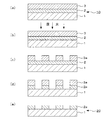
図1は、本発明のマスクブランクの一実施の形態を示す断面図である。これによると、本実施の形態に係るマスクブランク10は、透光性基板1上に、転写パターンを形成するための金属を含む材料からなる薄膜2を有する構造となっている。
FIG. 1 is a cross-sectional view showing an embodiment of a mask blank of the present invention. According to this, the mask blank 10 according to the present embodiment has a structure having a
上記透光性基板1は、使用する露光波長に対して透明性を有するものであれば特に制限されない。本発明では、石英基板、その他各種のガラス基板(例えば、ソーダライムガラス、アルミノシリケートガラス等)を用いることができるが、この中でも石英基板は、ArFエキシマレーザー又はそれよりも短波長の領域で透明性が高いので、本発明には特に好適である。
The said translucent board |
転写パターンを形成するための薄膜2は、遷移金属などの金属を含む材料からなる薄膜であり、単一層の場合も積層の場合も含まれる。積層の場合は、少なくとも最上層(最表面層)は上記金属を含む材料からなる層である。詳しくは後述するが、例えばクロム、タンタル、タングステンなどの遷移金属単体又はその化合物を含む材料からなる遮光膜や、遮光膜等の上に設けられるエッチングマスク膜などが挙げられる。また、遷移金属シリサイド(特にモリブデンシリサイド)の化合物を含む材料からなる光半透過膜や遮光膜なども挙げられる。
The
透光性基板1上に上記薄膜2を成膜する方法としては、例えばスパッタ成膜法が好ましく挙げられるが、本発明はスパッタ成膜法に限定する必要はない。
As a method for forming the
本発明のマスクブランク10は、上記薄膜2の表面(もしくは表層部分)に、炭化水素を含む酸化膜からなる表面改質層を有している。この表面改質層は、炭化水素を含む酸化膜であるが、この酸化膜中にはとくに炭化水素を含む酸化物(以下、有機系酸化物と呼ぶ。)が多く含まれるため、有機成分からなるレジストとの親和性が高く、レジストとの密着性を著しく向上させることができる。
The
上記薄膜2の表面(表層部分)に、上記有機系酸化物を含む表面改質層を形成する方法としては、例えば、薄膜の表面に高濃度オゾンガスと不飽和炭化水素ガスとを作用させる処理が挙げられる。因みに、従来、大気中あるいは大気中よりも酸素含有量の多い雰囲気下でマスクブランクを加熱処理することにより、薄膜の表面に酸化膜を形成させて、耐薬性等を向上させる方法が知られているが、この場合、雰囲気中の有機コンタミなどを含む酸化物が形成される可能性も考えられる。本発明者の検討によると、雰囲気中の有機コンタミによる有機成分が酸化膜中に含まれるとしてもほんの僅かであり、レジストとの密着性を向上させることは到底できないレベルである。また、耐薬性等を向上させるため高温度、長時間の加熱処理を行うと、薄膜の劣化や、表面粗さの劣化、光学特性の変化、マスクブランクの平坦度の変化を生じることは避けられず、マスクブランク性能の劣化を引き起こす恐れがある。これに対して、上述の高濃度オゾンガスと不飽和炭化水素ガスとを作用させる処理によれば、低温度かつ短時間で表面改質層を形成することができるので、薄膜の表面粗さや光学特性等を何ら劣化させることない。したがって、マスクブランクの特性を維持した状態で、薄膜の表面に有機系酸化物を多く含む酸化膜からなる表面改質層を形成することができるので、本発明に好適である。
As a method of forming the surface modification layer containing the organic oxide on the surface (surface layer portion) of the
本発明者の考察によれば、このように薄膜表面に対して、高濃度オゾンガスと不飽和炭化水素ガスとを作用させる(供給する)処理を行うことにより、オゾニド等の不安定な中間体が形成され、この不安定な中間体が分解される過程で、薄膜表面が改質され、有機系酸化物を含む酸化膜が形成されるものと考えられる。 According to the inventor's consideration, an unstable intermediate such as ozonide is obtained by performing (supplying) the high concentration ozone gas and the unsaturated hydrocarbon gas on the thin film surface in this way. In the process of being formed and decomposing this unstable intermediate, it is considered that the surface of the thin film is modified and an oxide film containing an organic oxide is formed.
薄膜表面に対して高濃度オゾンガスと不飽和炭化水素ガスとを作用させる方法としては、たとえば適当なチャンバー内にマスクブランクを設置し、このチャンバー内に高濃度オゾンガスと不飽和炭化水素ガスを導入して、マスクブランクの薄膜表面近傍にて混合させる方法が挙げられる。また、薄膜表面に対して直接高濃度オゾンガスと不飽和炭化水素ガスを噴き付けるなどの手段で供給する方法でもよい。なお、本発明による効果を良好に得るためには、高濃度オゾンガスと不飽和炭化水素ガスを薄膜表面近傍で混合させて作用させることが好適である。 As a method for allowing high concentration ozone gas and unsaturated hydrocarbon gas to act on the thin film surface, for example, a mask blank is installed in a suitable chamber, and high concentration ozone gas and unsaturated hydrocarbon gas are introduced into this chamber. And a method of mixing in the vicinity of the thin film surface of the mask blank. Alternatively, a method of supplying high-concentration ozone gas and unsaturated hydrocarbon gas directly to the surface of the thin film may be used. In order to obtain the effect of the present invention satisfactorily, it is preferable that high concentration ozone gas and unsaturated hydrocarbon gas are mixed and act in the vicinity of the thin film surface.
上記不飽和炭化水素としては、例えば、エチレン、ブチレン等の炭素の二重結合を有する炭化水素(アルケン)や、アセチレン等の炭素の三重結合を有する炭化水素(アルキン)などが挙げられ、特にこのような炭素数1〜4程度の低級不飽和炭化水素が好ましい。
また、オゾンガス濃度は、50〜100体積%の範囲であることが好ましい。オゾンガス濃度が50体積%未満であると、処理時間が非常に長く必要になったり、あるいは、処理時間を長くしても、レジストとの密着性の向上に必要な膜厚を確保できない恐れがある。また、処理時間を短時間にし、基板の加熱温度を低温度にして、表面変質層を形成することができるため、オゾンガス濃度は100体積%が好ましい。
オゾンガスと不飽和炭化水素ガスとの供給比率(流量比率)は、1:1〜4:1が好ましい。この範囲であれば、オゾンガスと不飽和炭化水素ガスとの反応が良好に行われる。
Examples of the unsaturated hydrocarbon include hydrocarbons having a carbon double bond (alkene) such as ethylene and butylene, hydrocarbons having a carbon triple bond such as acetylene (alkyne), and the like. Such a lower unsaturated hydrocarbon having about 1 to 4 carbon atoms is preferred.
Moreover, it is preferable that ozone gas concentration is the range of 50-100 volume%. If the ozone gas concentration is less than 50% by volume, the treatment time may be very long, or even if the treatment time is long, the film thickness necessary for improving the adhesion with the resist may not be secured. . Further, since the surface altered layer can be formed by shortening the treatment time and lowering the heating temperature of the substrate, the ozone gas concentration is preferably 100% by volume.
The supply ratio (flow rate ratio) between ozone gas and unsaturated hydrocarbon gas is preferably 1: 1 to 4: 1. If it is this range, reaction of ozone gas and unsaturated hydrocarbon gas will be performed favorably.
また、処理時間(高濃度オゾンガスと不飽和炭化水素ガスとを作用させる時間)については、オゾンガス濃度、基板の加熱温度、表面改質層の膜厚、被覆率等を考慮して適宜決定すればよい。
また、このような高濃度オゾンガスと不飽和炭化水素ガスとを作用させる表面改質処理は、室温で行うことができるが、薄膜表面に有機系酸化物を含む酸化膜が形成される反応をより促進させるため、例えば基板を、50℃〜80℃程度まで加熱してもよい。この場合の加熱温度があまり高いと、薄膜の材料にもよるが、例えばクロム系材料膜の場合、100℃を超えると膜が劣化する恐れがある。
Further, the processing time (time for allowing the high-concentration ozone gas and the unsaturated hydrocarbon gas to act) can be appropriately determined in consideration of the ozone gas concentration, the heating temperature of the substrate, the film thickness of the surface modification layer, the coverage, and the like. Good.
In addition, the surface modification treatment that causes the high-concentration ozone gas and the unsaturated hydrocarbon gas to act can be performed at room temperature, but the reaction of forming an oxide film containing an organic oxide on the thin film surface is more effective. In order to promote, for example, the substrate may be heated to about 50 ° C. to 80 ° C. If the heating temperature in this case is too high, depending on the material of the thin film, for example, in the case of a chromium-based material film, if the temperature exceeds 100 ° C., the film may deteriorate.
さらに、レジスト塗布前のマスクブランクは、収納ケース等に収められて一定期間保管されることがあり、保管状態によっては塩基性物質や有機物等の化学汚染物質が付着することがある。このような化学汚染物質は、特に化学増幅型レジストの機能の劣化(感度変動によるパターン形状の劣化、解像性の低下等)を生じさせてしまう。したがって、レジスト塗布前には、マスクブランクを洗浄し、このような化学汚染物質を除去する必要がある。上記高濃度オゾンガスと不飽和炭化水素ガスとを作用させると、表面改質と同時に、化学汚染物質をも除去することができるため、レジスト塗布前の洗浄処理をなくすことが可能となる。つまり、表面改質処理が洗浄処理を兼ねることが可能となる。 Furthermore, the mask blank before applying the resist may be stored in a storage case or the like and stored for a certain period of time, and chemical contaminants such as basic substances and organic substances may adhere depending on the storage state. Such chemical contaminants particularly cause deterioration of the function of the chemically amplified resist (deterioration of pattern shape due to sensitivity fluctuation, reduction of resolution, etc.). Therefore, before applying the resist, it is necessary to clean the mask blank and remove such chemical contaminants. When the high-concentration ozone gas and the unsaturated hydrocarbon gas are allowed to act, chemical contaminants can be removed at the same time as the surface modification, so that it is possible to eliminate the cleaning process before applying the resist. That is, the surface modification process can also serve as a cleaning process.
本発明のマスクブランク10において、薄膜の表面改質層の表面粗さ(Ra)は0.70nm以下である。本発明では、薄膜の表面に表面改質層が形成されることによる表面粗さの劣化を防止できるため、薄膜の表面、つまり表面改質層の表面の表面粗さをRa=0.70nm以下、さらにはRa=0.50nm以下に抑えることが可能である。
In the
表面粗さをRa=0.70nm以下、さらにはRa=0.50nm以下にすることにより、薄膜パターンのLER(Line EdgeRoughness)を小さくすることができると共に、薄膜パターンの断面形状も良好にすることができるので好ましい。本発明の高濃度オゾンガス処理によって薄膜に表面改質層を形成した場合、表面改質層形成前後において、表面粗さが変化しないか、又は小さくすることができる。
なお、本発明において、表面粗さを示す単位Raは、原子間力顕微鏡(AFM)で測定することができる。具体的な測定は、例えば1μm角の範囲内で行うが、マスクの有効エリア内で均一にこの表面粗さを有していることが好ましい。ここでマスクの有効エリアとは、6インチ基板の場合、例えば142mm角程度の範囲を有効エリアとして考えればよい。
By making the surface roughness Ra = 0.70 nm or less, and further Ra = 0.50 nm or less, the LER (Line EdgeRoughness) of the thin film pattern can be reduced, and the cross-sectional shape of the thin film pattern can be improved. Is preferable. When the surface modification layer is formed on the thin film by the high-concentration ozone gas treatment of the present invention, the surface roughness does not change or can be reduced before and after the surface modification layer formation.
In the present invention, the unit Ra indicating the surface roughness can be measured with an atomic force microscope (AFM). The specific measurement is performed within a range of 1 μm square, for example, and it is preferable that the surface roughness be uniform within the effective area of the mask. Here, the effective area of the mask may be a range of about 142 mm square, for example, in the case of a 6-inch substrate.
また、本発明の高濃度オゾンガス処理によって薄膜に表面改質層を形成した場合、表面改質層形成前後において、光学濃度(OD)及び露光光や検査光の波長に対する表面反射率がほとんど変化(劣化)しないようにすることができる。さらに、表面改質層形成前後において、平坦度の変化量(絶対値)は、30nm以下、さらには10nm以下とすることができる。
なお、本発明に記載する平坦度とはTIR(Total Indicated Reading)で表される表面の反り(変形量)を表す値である。本発明においては142×142mmのエリア内の測定値をもって平坦度とする。例えば、6インチ基板の中心における142×142mmのエリア内の測定値である。
In addition, when the surface modification layer is formed on the thin film by the high-concentration ozone gas treatment of the present invention, the optical density (OD) and the surface reflectance with respect to the wavelength of the exposure light or the inspection light almost change before and after the surface modification layer formation ( Deterioration). Further, the amount of change in flatness (absolute value) before and after the formation of the surface modified layer can be 30 nm or less, and further 10 nm or less.
The flatness described in the present invention is a value representing the warpage (deformation amount) of the surface expressed by TIR (Total Indicated Reading). In the present invention, the measured value in an area of 142 × 142 mm is defined as flatness. For example, a measurement value within an area of 142 × 142 mm at the center of a 6-inch substrate.
このように、光学濃度、表面反射率及び平坦度変化量を劣化させることがないので、マスクブランクや転写用マスクの性能に影響を及ぼさない。また、表面改質層が形成された薄膜をパターニングして転写用マスクを作製する際に、薄膜のエッチング特性を低下させることはないため、転写要マスクの加工精度を低下させることもない。
また、ダブルパターニング/ダブル露光技術を用いる転写用マスクにも好適である。これらの露光技術は2枚セットの転写用マスクを用いるものであるため、2枚の転写用マスクの精度の要求が厳しいが、本発明はこのような要求を満たすことが可能となる。また、特に転写用マスクとしたときにエッチングマスク膜を剥離するタイプのマスクブランクにおけるエッチングマスク膜に表面改質層を形成した場合には、エッチングマスク膜パターンをマスクにして下層膜を良好にエッチングすることが可能となり、またマスクブランクの欠陥検査等の検査を良好に行うことが可能となる。
As described above, since the optical density, the surface reflectance, and the flatness change amount are not deteriorated, the performance of the mask blank or the transfer mask is not affected. Further, when the transfer mask is manufactured by patterning the thin film on which the surface modification layer is formed, the etching characteristics of the thin film are not deteriorated, so that the processing accuracy of the transfer required mask is not lowered.
It is also suitable for a transfer mask using a double patterning / double exposure technique. Since these exposure techniques use a set of two transfer masks, the accuracy of the two transfer masks is severely demanded, but the present invention can satisfy such a requirement. In particular, when a surface modification layer is formed on the etching mask film of a mask blank that peels off the etching mask film when used as a transfer mask, the lower layer film is etched well using the etching mask film pattern as a mask. In addition, it is possible to satisfactorily perform inspections such as mask blank defect inspection.
図3は、後述の実施例1における表面改質層のX線光電子分光法(XPS)による分析結果を示したものであり、(a)は表面改質層のO(酸素)1sスペクトル、(b)は上述の高濃度オゾンガスと不飽和炭化水素ガスによる表面改質処理による表面改質層が形成されていない状態の遮光膜の表層部分のO1sスペクトルである。また、図4は、同じく実施例1における表面改質層のX線光電子分光法(XPS)による分析結果を示したものであり、(a)は表面改質層のC(炭素)1sスペクトル、(b)は上述の表面改質処理による表面改質層が形成されていない状態の遮光膜の表層部分のC1sスペクトルである。 FIG. 3 shows the analysis result of the surface modified layer in X-ray photoelectron spectroscopy (XPS) in Example 1 to be described later, (a) is the O (oxygen) 1s spectrum of the surface modified layer, ( b) is an O1s spectrum of the surface layer portion of the light-shielding film in a state where the surface modification layer is not formed by the surface modification treatment with the high-concentration ozone gas and the unsaturated hydrocarbon gas. FIG. 4 also shows the analysis result of the surface modified layer in Example 1 by X-ray photoelectron spectroscopy (XPS), (a) shows the C (carbon) 1s spectrum of the surface modified layer, (B) is a C1s spectrum of the surface layer portion of the light-shielding film in a state where the surface-modified layer formed by the surface modification treatment is not formed.
詳しくは実施例1で後述するが、実施例1は、透光性基板上にMoSi系材料からなる光半透過膜とCr系材料からなる遮光膜をこの順に積層し、高濃度オゾンガスとエチレンガスとを遮光膜に作用させる処理により上記遮光膜の表面に表面改質層を形成した位相シフトマスクブランクに関するものである。
上記表面改質層は、XPSによって測定されるO1sスペクトルにおいて、結合エネルギーがそれぞれ532eV付近にある第1のピークと530eV付近にある第2のピークとに分離したときに、第2のピーク面積に対する第1のピーク面積の割合が2.0以上である。上記第1のピークは、主に有機系酸化物成分や酸化度の高いクロム酸化物(Cr2O3など)成分(これらをA成分とする)によるピークであり、上記第2のピークは、主に酸化度の低いクロム酸化物(CrOなど)成分やクロム酸窒化物成分(これらをB成分とする)によるピークである。また、XPSによって測定されるC1sスペクトルにおいて、有機系酸化物成分による炭酸塩(H2CO3の塩)のピークが確認できる。
Although details will be described later in Example 1, in Example 1, a light semi-transmissive film made of MoSi-based material and a light-shielding film made of Cr-based material are laminated in this order on a light-transmitting substrate, and high-concentration ozone gas and ethylene gas are stacked. The present invention relates to a phase shift mask blank in which a surface modification layer is formed on the surface of the light-shielding film by a treatment that causes the light-shielding film to act.
When the surface modification layer is separated into a first peak near 532 eV and a second peak near 530 eV in the O1s spectrum measured by XPS, The ratio of the first peak area is 2.0 or more. The first peak is a peak mainly due to an organic oxide component or a highly oxidized chromium oxide (Cr 2 O 3 etc.) component (these are referred to as A component), and the second peak is It is a peak mainly due to a chromium oxide (CrO or the like) component having a low degree of oxidation or a chromic oxynitride component (which is referred to as B component). Moreover, in the C1s spectrum measured by XPS, the peak of carbonate (H 2 CO 3 salt) due to the organic oxide component can be confirmed.
この分析結果から、A成分は74%、B成分は26%であり、パターン形成用の薄膜の表面に上述の表面改質層が形成されることにより、表面改質層が形成されていない状態(上記図3(b)及び図4(b)のスペクトル)と比べると、上記A成分の割合が増加(B成分の割合は減少)していると共に、炭酸塩の割合が増加しており、薄膜表面を、有機系酸化物を含む酸化膜(表面改質層)とすることにより、レジストとの密着性が向上するものと考えられる。 From this analysis result, the A component is 74%, the B component is 26%, and the surface modified layer is not formed by forming the surface modified layer on the surface of the pattern forming thin film. Compared to the above (spectra of FIG. 3 (b) and FIG. 4 (b)), the proportion of the A component is increased (the proportion of the B component is decreased), and the proportion of the carbonate is increased, By making the surface of the thin film an oxide film (surface modified layer) containing an organic oxide, it is considered that the adhesion to the resist is improved.
なお、上記表面改質層の膜厚は、本発明においては特に制約はされないが、レジストとの密着性向上効果を十分に得るためには、少なくとも1nm以上であることが好ましい。また、表面改質層の膜厚を厚くするためには、例えば上述の高濃度オゾンガスと不飽和炭化水素ガスによる処理時間を長くする必要がある上に、膜厚があまり厚いと光学特性変化が大きくなる恐れがある。そのため、レジストとの密着性の向上が十分に達成できる膜厚とすればよく、その観点から3nm以下とすることが好ましい。
なお、表面改質層の存在は、例えば薄膜の断面TEM観察により確認することが可能であり、表面改質層の膜厚についても特定することが可能である。
The film thickness of the surface modified layer is not particularly limited in the present invention, but is preferably at least 1 nm or more in order to sufficiently obtain the effect of improving the adhesion to the resist. In addition, in order to increase the film thickness of the surface modification layer, for example, it is necessary to lengthen the treatment time with the above-described high-concentration ozone gas and unsaturated hydrocarbon gas. There is a risk of growing. Therefore, the film thickness may be a thickness that can sufficiently improve the adhesion to the resist, and from the viewpoint, it is preferably 3 nm or less.
The presence of the surface modified layer can be confirmed, for example, by TEM observation of the thin film, and the film thickness of the surface modified layer can also be specified.
なお、図1に示すマスクブランク10は、上記薄膜2上にレジスト膜を備えていないが、本発明は、薄膜2上に任意のレジスト膜を備えた構造のマスクブランクも含まれる。
また、本発明は、特に化学増幅型レジスト膜を備えたマスクブランクが好適である。レジスト膜付きマスクブランクは、収納ケース等に収められて一定期間保管されることが多い。長期間(例えば40日以上)保管されたレジスト膜付きマスクブランクを用いて転写用マスクを作製した場合、形成したレジストパターン形状が劣化するという問題があることがわかった。これは、レジスト膜下の薄膜表面に存在する汚染物質(汚染イオン等)が、長期間の保管中にレジスト膜中に入り込み、化学増幅型レジストの機能を劣化(感度変動によるパターン形状の劣化、解像性の低下等)させることが要因であると考えられる。これにより、レジストパターンの裾部分において、ポジ型の化学増幅型レジスト膜においては「裾引き」、ネガ型では「食われ」といった形状不良が生じてしまう。特に、ネガ型の場合には、「食われ」によって、レジストパターン倒れが生じる。
本発明の表面改質層を有する薄膜上に形成されたレジスト膜付きマスクブランクは、長期間保管した後に転写用マスクを作製しても、上記レジストパターン形状の劣化を防止することができる。これは、上記表面改質層を形成する過程において、薄膜表面上の汚染物質が除去されたり、表面改質層によって汚染物質がレジスト膜中に入り込むことが防止されたりするからであると考えられる。
Although the mask blank 10 shown in FIG. 1 does not include a resist film on the
In the present invention, a mask blank provided with a chemically amplified resist film is particularly suitable. The mask blank with a resist film is often stored in a storage case or the like and stored for a certain period. It has been found that when a mask for transfer is prepared using a mask blank with a resist film that has been stored for a long period (for example, 40 days or longer), the formed resist pattern shape is deteriorated. This is because contaminants (contaminated ions, etc.) present on the surface of the thin film under the resist film enter the resist film during long-term storage and degrade the function of the chemically amplified resist (deterioration of pattern shape due to sensitivity fluctuations, This is considered to be caused by a decrease in resolution. As a result, in the skirt portion of the resist pattern, a shape defect such as “bottoming” occurs in the positive chemically amplified resist film and “erosion” occurs in the negative type. In particular, in the case of the negative type, the resist pattern collapses due to “eating”.
Even if the mask blank with a resist film formed on the thin film having the surface modified layer of the present invention is stored for a long period of time, the resist pattern shape can be prevented from deteriorating even if a transfer mask is prepared. This is considered to be because contaminants on the surface of the thin film are removed in the process of forming the surface modified layer, or the contaminants are prevented from entering the resist film by the surface modified layer. .
図2は、本発明のマスクブランクを用いて転写用マスクを製造する工程を示す断面図である。
透光性基板1上に、上記薄膜2を成膜し、その表面に表面改質層を形成したマスクブランク10を用いて、フォトリソグラフィー法により、該マスクブランクの薄膜をパターニングすることにより、薄膜パターンを形成する。すなわち、上記マスクブランク10の表面に、例えば電子線描画用ポジ型レジスト膜3を形成し(同図(a)参照)、所望のデバイスパターンの描画を行う(同図(b)参照)。描画後、レジスト膜3を現像処理することにより、レジストパターン3aを形成する(同図(c)参照)。本発明のマスクブランクは、レジストとの密着性が良好であるため、たとえレジストパターンの線幅がレジスト膜厚の1/3未満であっても、レジストパターンの倒れや欠けなどの発生を抑制することができる。
FIG. 2 is a cross-sectional view showing a process of manufacturing a transfer mask using the mask blank of the present invention.
The
次に、このレジストパターン3aをマスクとして、上記薄膜2をエッチングすることにより、薄膜パターン2aを形成することができる(同図(d)参照)。この際のエッチング方法としては、微細パターンの形成に有効なドライエッチングを好ましく用いることができる。
残存するレジストパターンを除去して、透光性基板1上に薄膜パターン2aを形成した転写用マスク20が出来上がる(同図(e)参照)。
本発明のマスクブランクを用いることにより、パターン倒れや欠けなどを生じることなく、微細なレジストパターンを安定して形成することができるため、最終的に微細転写パターンが高い精度で形成された転写用マスクを作製することが可能である。
Next, the
The remaining resist pattern is removed, and a
By using the mask blank of the present invention, a fine resist pattern can be stably formed without causing pattern collapse or chipping, so that the fine transfer pattern is finally formed with high accuracy. It is possible to make a mask.
なお、従来、遷移金属シリサイド化合物(例えばモリブデンシリサイド化合物)などを含む材料の場合には、レジストとの密着性を確保するため、レジスト塗布前に、HMDS(ヘキサメチルジシラザン:Hexamethyldisilazane)などのシラン系カップリング剤による表面処理を施すことが行われているが、本発明によれば、マスクブランクの薄膜の材料の種類にかかわらず、レジストとの密着性、とりわけ化学増幅型レジストとの密着性を向上できるというメリットがある。
また、転写用マスクを作製する工程において、複数回レジストを塗布する必要がある場合には、レジストを塗布する処理前毎に本発明の表面改質層を形成する処理を施してもよい。例えば、ハーフトーン型位相シフトマスク、トライトーン型位相シフトマスク、エンハンサ型位相シフトマスク等を作製する工程において、最初に塗布されて残存したレジストパターンを除去して、再度全面にレジスト膜を形成し、マスクの外周部等に遮光部(遮光帯)を形成する場合に、該レジスト膜を形成する前に、本発明の表面改質層を形成する処理を施すことができる。
Conventionally, in the case of a material containing a transition metal silicide compound (for example, a molybdenum silicide compound), a silane such as HMDS (Hexamethyldisilazane) is applied before resist application to ensure adhesion with the resist. Although surface treatment with a coupling agent is performed, according to the present invention, regardless of the material of the mask blank thin film, adhesion to the resist, particularly adhesion to the chemically amplified resist There is an advantage that can be improved.
Further, in the step of producing a transfer mask, when it is necessary to apply a resist a plurality of times, a process for forming the surface modified layer of the present invention may be performed before the process of applying the resist. For example, in the process of manufacturing a halftone phase shift mask, a tritone phase shift mask, an enhancer phase shift mask, etc., the resist pattern that has been applied first is removed, and a resist film is formed again on the entire surface. In the case where a light shielding part (light shielding band) is formed on the outer peripheral part or the like of the mask, the surface modifying layer of the present invention can be formed before the resist film is formed.
以上の実施の形態により説明したように、本発明は、とくに微細転写パターンが要求される波長200nm以下の短波長の露光光を露光光源とする露光装置に用いられる転写用マスクの製造に用いるマスクブランクに好適である。例えば、以下のようなマスクブランクおよびその製造並びに転写用マスクに好適である。 As described in the above embodiment, the present invention is a mask used for manufacturing a transfer mask used in an exposure apparatus using an exposure light source with a short wavelength exposure light having a wavelength of 200 nm or less, in particular, where a fine transfer pattern is required. Suitable for blanks. For example, the present invention is suitable for the following mask blanks and their production and transfer masks.
(1)前記薄膜が遷移金属を含む材料からなる遮光膜であるバイナリマスクブランクおよびバイナリマスク
かかるバイナリマスクブランクは、透光性基板上に遮光膜を有する形態のものであり、この遮光膜は、クロム、タンタル、ルテニウム等の遷移金属単体あるいはその化合物を含む材料からなる。例えば、クロムや、クロムに酸素、窒素、炭素などの元素から選ばれる1種以上の元素を添加したクロム化合物で構成した遮光膜が挙げられる。また、例えば、タンタルに、酸素、窒素、ホウ素などの元素から選ばれる1種以上の元素を添加したタンタル化合物で構成した遮光膜が挙げられる。また、上記遷移金属と、アルミニウム、マグネシウム、ガリウム、ゲルマニウム、スズ等の金属とを含む合金又はそれに酸素、窒素、炭素などの元素から選ばれる1種以上の元素を添加した化合物としてもよい。
かかるバイナリマスクブランクは、遮光膜を、遮光層と表面反射防止層の2層構造や、さらに遮光層と基板との間に裏面反射防止層を加えた3層構造としたものなどがある。また、遮光膜の膜厚方向における組成が連続的又は段階的に異なる組成傾斜膜としてもよい。
(1) A binary mask blank and a binary mask, which are light shielding films made of a material containing a transition metal as the thin film. The binary mask blank has a light shielding film on a light-transmitting substrate. It consists of a material containing a transition metal alone or a compound thereof such as chromium, tantalum, ruthenium. For example, a light-shielding film composed of chromium or a chromium compound in which one or more elements selected from elements such as oxygen, nitrogen, and carbon are added to chromium. Further, for example, a light shielding film composed of a tantalum compound in which one or more elements selected from elements such as oxygen, nitrogen, and boron are added to tantalum. Alternatively, an alloy including the above transition metal and a metal such as aluminum, magnesium, gallium, germanium, or tin, or a compound in which one or more elements selected from elements such as oxygen, nitrogen, and carbon are added thereto may be used.
Such binary mask blanks include a light shielding film having a two-layer structure of a light shielding layer and a front surface antireflection layer, or a three-layer structure in which a back surface antireflection layer is added between the light shielding layer and the substrate. Moreover, it is good also as a composition gradient film | membrane from which the composition in the film thickness direction of a light shielding film differs continuously or in steps.
(2)前記薄膜が、遷移金属及びケイ素(遷移金属シリサイド、特にモリブデンシリサイドを含む)の化合物を含む材料からなる光半透過膜である位相シフトマスクブランクおよび位相シフトマスク
かかる位相シフトマスクブランクとしては、透光性基板上に光半透過膜を有する形態のものであって、該光半透過膜をパターニングしてシフタ部を設けるタイプであるハーフトーン型位相シフトマスクが作製される。かかる位相シフトマスクにおいては、光半透過膜を透過した光に基づき転写領域に形成される光半透過膜パターンによる被転写基板のパターン不良を防止するために、透光性基板上に光半透過膜とその上の遮光膜(遮光帯)とを有する形態とするものが挙げられる。また、ハーフトーン型位相シフトマスクブランクのほかに、透光性基板をエッチング等により掘り込んでシフタ部を設ける基板掘り込みタイプであるレベンソン型位相シフトマスク用やエンハンサー型位相シフトマスク用のマスクブランクが挙げられる。
(2) Phase shift mask blank and phase shift mask in which the thin film is a light semi-transmissive film made of a material containing a compound of transition metal and silicon (including transition metal silicide, particularly molybdenum silicide). Thus, a halftone phase shift mask having a light semi-transmissive film on a light-transmitting substrate and having a shifter portion by patterning the light semi-transmissive film is manufactured. In such a phase shift mask, in order to prevent a pattern defect of the transferred substrate due to the light semi-transmissive film pattern formed in the transfer region based on the light transmitted through the light semi-transmissive film, the light semi-transmissive is formed on the light-transmissive substrate. The thing which has a form which has a film | membrane and the light shielding film (light shielding zone) on it is mentioned. In addition to halftone phase shift mask blanks, mask blanks for Levenson type phase shift masks and enhancer type phase shift masks, which are substrate digging types in which a translucent substrate is dug by etching or the like to provide a shifter portion. Is mentioned.
上記光半透過膜は、実質的に露光に寄与しない強度の光(例えば、露光波長に対して1%〜30%)を透過させるものであって、所定の位相差(例えば180度)を有するものであり、この光半透過膜をパターニングした光半透過部と、光半透過膜が形成されていない実質的に露光に寄与する強度の光を透過させる光透過部とによって、光半透過部を透過して光の位相が光透過部を透過した光の位相に対して実質的に反転した関係になるようにすることによって、光半透過部と光透過部との境界部近傍を通過し回折現象によって互いに相手の領域に回り込んだ光が互いに打ち消しあうようにし、境界部における光強度をほぼゼロとし境界部のコントラスト即ち解像度を向上させるものである。 The light semi-transmissive film transmits light having an intensity that does not substantially contribute to exposure (for example, 1% to 30% with respect to the exposure wavelength) and has a predetermined phase difference (for example, 180 degrees). The light semi-transmissive portion is formed by patterning the light semi-transmissive film, and the light transmissive portion that does not have the light semi-transmissive film and transmits light having an intensity substantially contributing to exposure. So that the phase of the light is substantially inverted with respect to the phase of the light transmitted through the light transmitting portion, so that the light passes through the vicinity of the boundary between the light semi-transmitting portion and the light transmitting portion. Lights that have sneak into each other due to the diffraction phenomenon cancel each other, and the light intensity at the boundary is made almost zero to improve the contrast or resolution of the boundary.
この光半透過膜は、例えば遷移金属及びケイ素(遷移金属シリサイドを含む)の化合物を含む材料からなり、これらの遷移金属及びケイ素と、酸素及び/又は窒素を主たる構成要素とする材料が挙げられる。遷移金属には、モリブデン、タンタル、タングステン、チタン、ハフニウム、ニッケル、バナジウム、ジルコニウム、ニオブ、パラジウム、ルテニウム、ロジウム等が適用可能である。
また、光半透過膜上に遮光膜を有する形態の場合、上記光半透過膜の材料が遷移金属及びケイ素を含むので、遮光膜の材料としては、光半透過膜に対してエッチング選択性を有する(エッチング耐性を有する)特にクロムや、クロムに酸素、窒素、炭素などの元素を添加したクロム化合物で構成することが好ましい。
This light semi-transmissive film is made of a material containing a compound of, for example, a transition metal and silicon (including a transition metal silicide), and includes a material mainly composed of these transition metal and silicon, and oxygen and / or nitrogen. . As the transition metal, molybdenum, tantalum, tungsten, titanium, hafnium, nickel, vanadium, zirconium, niobium, palladium, ruthenium, rhodium, or the like is applicable.
In the case of having a light-shielding film on the light semi-transmissive film, the material of the light semi-transmissive film contains a transition metal and silicon. It is preferable to have chromium (having etching resistance), particularly chromium, or a chromium compound in which elements such as oxygen, nitrogen, and carbon are added to chromium.
(3)前記薄膜が、遷移金属及びケイ素(遷移金属シリサイド、特にモリブデンシリサイドを含む)、又は遷移金属及びケイ素の化合物を含む材料からなる遮光膜であるバイナリマスクブランクおよびバイナリマスク
この遮光膜は、遷移金属及びケイ素の化合物を含む材料からなり、これらの遷移金属及びケイ素と、酸素及び/又は窒素を主たる構成要素とする材料が挙げられる。また、遮光膜は、遷移金属と、酸素、窒素及び/又はホウ素を主たる構成要素とする材料が挙げられる。遷移金属には、モリブデン、タンタル、タングステン、チタン、ハフニウム、ニッケル、バナジウム、ジルコニウム、ニオブ、パラジウム、ルテニウム、ロジウム等が適用可能である。
特に、遮光膜をモリブデンシリサイドの化合物で形成する場合であって、遮光層(MoSi等)と表面反射防止層(MoSiON等)の2層構造や、さらに遮光層と基板との間に裏面反射防止層(MoSiON等)を加えた3層構造がある。
また、遮光膜の膜厚方向における組成が連続的又は段階的に異なる組成傾斜膜としてもよい。
(3) Binary mask blank and binary mask in which the thin film is a light-shielding film made of a material containing transition metal and silicon (including transition metal silicide, particularly molybdenum silicide), or a compound of transition metal and silicon. Examples thereof include a material containing a compound of a transition metal and silicon, and a material mainly composed of these transition metal and silicon and oxygen and / or nitrogen. Examples of the light shielding film include a material mainly composed of a transition metal and oxygen, nitrogen, and / or boron. As the transition metal, molybdenum, tantalum, tungsten, titanium, hafnium, nickel, vanadium, zirconium, niobium, palladium, ruthenium, rhodium, or the like is applicable.
In particular, when the light shielding film is formed of a molybdenum silicide compound, it has a two-layer structure of a light shielding layer (MoSi, etc.) and a surface antireflection layer (MoSiON, etc.), and the back surface antireflection between the light shielding layer and the substrate There is a three-layer structure to which layers (MoSiON, etc.) are added.
Moreover, it is good also as a composition gradient film | membrane from which the composition in the film thickness direction of a light shielding film differs continuously or in steps.
また、レジスト膜の膜厚を薄膜化して微細パターンを形成するために、遮光膜上にエッチングマスク膜を有する構成としてもよい。このエッチングマスク膜は、遷移金属シリサイドを含む遮光膜のエッチングに対してエッチング選択性を有する(エッチング耐性を有する)特にクロムや、クロムに酸素、窒素、炭素などの元素を添加したクロム化合物からなる材料(クロム系材料)で構成することが好ましい。また、遮光膜がクロム系材料からなる場合には、エッチングマスク膜はケイ素に酸素、窒素などの元素を添加したケイ素化合物、又はそれらにモリブデンなどの遷移金属を添加した材料で構成することが好ましい。さらに、遮光膜がタンタルやタンタルに酸素、窒素などの元素を添加したタンタル化合物からなる材料で構成される場合には、エッチングマスク膜はクロム系材料で構成することが好ましい。このとき、エッチングマスク膜に反射防止機能を持たせることにより、遮光膜上にエッチングマスク膜を残した状態で転写用マスクを作製してもよい。 In order to form a fine pattern by reducing the thickness of the resist film, an etching mask film may be provided over the light shielding film. This etching mask film has etching selectivity (etching resistance) with respect to etching of the light-shielding film containing transition metal silicide, and in particular, chromium, or a chromium compound in which elements such as oxygen, nitrogen, and carbon are added to chromium. It is preferable to comprise a material (chromium-based material). When the light-shielding film is made of a chromium-based material, the etching mask film is preferably composed of a silicon compound obtained by adding an element such as oxygen or nitrogen to silicon, or a material obtained by adding a transition metal such as molybdenum thereto. . Furthermore, when the light shielding film is made of tantalum or a material made of a tantalum compound obtained by adding an element such as oxygen or nitrogen to tantalum, the etching mask film is preferably made of a chromium-based material. At this time, by providing the etching mask film with an antireflection function, the transfer mask may be manufactured with the etching mask film remaining on the light shielding film.
また、(1)〜(3)において、透光性基板と遮光膜との間、又は光半透過膜と遮光膜との間に、遮光膜や光半透過膜に対してエッチング耐性を有するエッチングストッパー膜を設けてもよい。エッチングストッパー膜は、エッチングストッパー膜をエッチングするときにエッチングマスク膜を同時に剥離することができる材料としてもよい。 Further, in (1) to (3), etching having etching resistance with respect to the light shielding film and the light semitransmissive film between the light transmissive substrate and the light shielding film or between the light semitransmissive film and the light shielding film. A stopper film may be provided. The etching stopper film may be a material that can peel off the etching mask film at the same time when the etching stopper film is etched.
(4)前記薄膜が、タンタルを含む材料からなる吸収体膜である反射型マスクブランク及び反射型マスク
かかる反射型マスクは、基板上に露光光を反射する多層反射膜が形成され、該多層反射膜上にバッファ膜、さらにその上に露光光を吸収する吸収体膜がパターン状に形成されたものである。バッファ膜は、吸収体膜のパターン形成工程及び修正工程における多層反射膜の保護を目的として多層反射膜と吸収体膜との間に設けられており、バッファ膜がない構成とすることもできる。
吸収体膜は、露光光である例えばEUV光を吸収する機能を有するものであれば良い。タンタルを含む材料としては、特にTaの単体またはTaを主成分とする材料を好ましく用いることができる。Taを主成分とする材料は、たとえばTaの合金である。このような吸収体膜の結晶状態は、平滑性、平坦性の点から、アモルファス状又は微結晶の構造を有しているものが好ましい。Taを主成分とする材料としては、例えばTaとBを含む材料、TaとNを含む材料、TaとBを含み、更にOとNの少なくとも何れかを含む材料、等を好適に用いることができる。
(4) A reflective mask blank and a reflective mask in which the thin film is an absorber film made of a material containing tantalum. The reflective mask includes a multilayer reflective film that reflects exposure light on a substrate, and the multilayer reflective film. A buffer film is formed on the film, and an absorber film that absorbs exposure light is formed in a pattern on the buffer film. The buffer film is provided between the multilayer reflective film and the absorber film for the purpose of protecting the multilayer reflective film in the pattern forming process and the correction process of the absorber film, and may be configured without the buffer film.
The absorber film only needs to have a function of absorbing exposure light such as EUV light. As the material containing tantalum, a simple substance of Ta or a material mainly containing Ta can be preferably used. The material mainly composed of Ta is an alloy of Ta, for example. Such an absorber film preferably has an amorphous or microcrystalline structure in terms of smoothness and flatness. As the material mainly composed of Ta, for example, a material containing Ta and B, a material containing Ta and N, a material containing Ta and B, and further containing at least one of O and N are preferably used. it can.
また、基板としては、SiO2−TiO2系ガラス、石英ガラス、結晶化ガラスであれば、β石英固溶体を析出した結晶化ガラス等を用いることができる。金属基板の例としては、インバー合金(Fe−Ni系合金)などが挙げられる。また、単結晶シリコン基板を使用することもできる。
転写用マスクには、位相シフト効果を使用しないバイナリマスク、位相シフト効果を使用する位相シフトマスクの中では、ハーフトーン型位相シフトマスク、レベンソン型位相シフトマスク、エンハンサーマスク、反射型マスクなどが含まれる。転写用マスクにはレチクルが含まれる。
Further, as the substrate, for example, crystallized glass in which a β-quartz solid solution is precipitated can be used as long as it is SiO 2 —TiO 2 glass, quartz glass, or crystallized glass. Examples of metal substrates include Invar alloys (Fe—Ni alloys). A single crystal silicon substrate can also be used.
Transfer masks include binary masks that do not use the phase shift effect, and phase shift masks that use the phase shift effect include halftone phase shift masks, Levenson type phase shift masks, enhancer masks, and reflective masks. It is. The transfer mask includes a reticle.
また、以上説明したような転写用マスクとは使用目的が異なるが、ガラス材料からなる基板の主表面上に基板掘り込みパターン形成用の薄膜を備えるマスクブランクにおいて、上記基板上に薄膜を成膜した後、前記薄膜上にレジスト膜を形成するインプリント用モールドの作製方法においても、本発明を適用することができる。 Although the purpose of use is different from the transfer mask as described above, a thin film is formed on the substrate in a mask blank including a thin film for forming a substrate digging pattern on the main surface of a substrate made of a glass material. Then, the present invention can also be applied to a method for producing an imprint mold in which a resist film is formed on the thin film.
半導体デバイスの微細回路パターン、微細パターンにより光学的機能を付加した光学部品作製、ハードディスクドライブ等に用いられる磁気記録媒体における磁性層の微細パターン形成に使用するインプリント用モールド(スタンパ)の作製においては、合成石英ガラスなどのガラス基板上に基板掘り込みパターン形成用の薄膜を備えたマスクブランクが用いられる。このマスクブランク上に所望のレジストパターンを形成し、このレジストパターンをマスクとして上記薄膜をエッチング加工することにより薄膜パターンを形成し、さらにこの薄膜パターンをマスクとして、上記基板をエッチング加工して、透光性基板に段差パターン(マスクパターン)を形成することにより、インプリント用モールドを作製している。
本発明は、このようなインプリント用モールドの作製方法において、レジスト膜を形成する前に、例えばクロム系材料からなる上記薄膜に対して、上述の高濃度オゾンガスと不飽和炭化水素ガスによる処理を適用することが好ましい。
In the production of imprint molds (stampers) used for fine pattern formation of magnetic layers in magnetic recording media used in hard disk drives, etc. A mask blank provided with a thin film for forming a substrate digging pattern on a glass substrate such as synthetic quartz glass is used. A desired resist pattern is formed on the mask blank, the thin film is etched by using the resist pattern as a mask, and the substrate is etched by using the thin film pattern as a mask. An imprint mold is produced by forming a step pattern (mask pattern) on the optical substrate.
According to the present invention, in such a method for producing an imprint mold, before the resist film is formed, the thin film made of, for example, a chromium-based material is treated with the high-concentration ozone gas and the unsaturated hydrocarbon gas. It is preferable to apply.
以下、実施例により、本発明の実施の形態を更に具体的に説明する。
(実施例1)
透光性基板としてサイズ6インチ角、厚さ0.25インチの合成石英ガラス基板を用い、透光性基板上に、まず窒化されたモリブデン及びシリコンからなる光半透過膜を成膜した。
具体的には、モリブデン(Mo)とシリコン(Si)との混合ターゲット(Mo:Si=10mol%:90mol%)を用い、アルゴン(Ar)と窒素(N2)とヘリウム(He)との混合ガス雰囲気(ガス流量比 Ar:N2:He=5:49:46)で、ガス圧0.3Pa、DC電源の電力を3.0kWとして、反応性スパッタリング(DCスパッタリング)により、モリブデン、シリコン及び窒素からなるMoSiN膜を69nmの膜厚で形成した。次いで、上記MoSiN膜が形成された基板に対して、加熱炉を用いて、大気中で加熱温度を450℃、加熱時間を1時間として、加熱処理を行った。なお、このMoSiN膜は、ArFエキシマレーザーにおいて、透過率は6.16%、位相差が184.4度となっていた。
Hereinafter, the embodiment of the present invention will be described more specifically with reference to examples.
Example 1
A synthetic quartz glass substrate having a size of 6 inches square and a thickness of 0.25 inches was used as the light transmitting substrate, and a light semi-transmitting film made of nitrided molybdenum and silicon was first formed on the light transmitting substrate.
Specifically, using a mixed target of molybdenum (Mo) and silicon (Si) (Mo: Si = 10 mol%: 90 mol%), mixing argon (Ar), nitrogen (N 2 ), and helium (He). In a gas atmosphere (gas flow ratio Ar: N 2 : He = 5: 49: 46), a gas pressure of 0.3 Pa, a DC power source power of 3.0 kW, and reactive sputtering (DC sputtering), molybdenum, silicon, and A MoSiN film made of nitrogen was formed to a thickness of 69 nm. Next, the substrate on which the MoSiN film was formed was subjected to heat treatment using a heating furnace in the atmosphere at a heating temperature of 450 ° C. and a heating time of 1 hour. This MoSiN film had an transmittance of 6.16% and a phase difference of 184.4 degrees in an ArF excimer laser.
次に、上記光半透過膜の上に、以下の遮光膜を成膜した。
具体的には、スパッタターゲットにクロム(Cr)ターゲットを用い、アルゴン(Ar)と二酸化炭素(CO2)と窒素(N2)とヘリウム(He)との混合ガス雰囲気(ガス圧0.2Pa,ガス流量比 Ar:CO2:N2:He=20:35:10:30)とし、DC電源の電力を1.7kWとし、反応性スパッタリング(DCスパッタリング)により、膜厚30nmのCrOCN層を成膜した。続いて、アルゴン(Ar)と窒素(N2)との混合ガス雰囲気(ガス圧0.1Pa,ガス流量比 Ar:N2=25:5)とし、DC電源の電力を1.7kWとし、反応性スパッタリング(DCスパッタリング)により、膜厚4nmのCrN層を成膜した。最後に、アルゴン(Ar)と二酸化炭素(CO2)と窒素(N2)とヘリウム(He)との混合ガス雰囲気(ガス圧0.2Pa,ガス流量比 Ar:CO2:N2:He=20:35:5:30)とし、DC電源の電力を1.7kWとし、反応性スパッタリング(DCスパッタリング)により、膜厚14nmのCrOCN層を成膜し、合計膜厚48nmの3層積層構造のクロム系遮光膜を形成した。
Next, the following light shielding film was formed on the light semi-transmissive film.
Specifically, a chromium (Cr) target is used as a sputtering target, and a mixed gas atmosphere of argon (Ar), carbon dioxide (CO 2 ), nitrogen (N 2 ), and helium (He) (gas pressure 0.2 Pa, Gas flow ratio Ar: CO 2 : N 2 : He = 20: 35: 10: 30), the power of the DC power source is 1.7 kW, and a 30 nm thick CrOCN layer is formed by reactive sputtering (DC sputtering). Filmed. Subsequently, a mixed gas atmosphere of argon (Ar) and nitrogen (N 2 ) (gas pressure 0.1 Pa, gas flow ratio Ar: N 2 = 25: 5) was set, and the power of the DC power source was set to 1.7 kW. A 4 nm thick CrN layer was formed by reactive sputtering (DC sputtering). Finally, a mixed gas atmosphere of argon (Ar), carbon dioxide (CO 2 ), nitrogen (N 2 ), and helium (He) (gas pressure 0.2 Pa, gas flow ratio Ar: CO 2 : N 2 : He = 20: 35: 5: 30), the power of the DC power source is 1.7 kW, and a CrOCN layer having a film thickness of 14 nm is formed by reactive sputtering (DC sputtering). A chromium-based light shielding film was formed.
この遮光膜は、上記光半透過膜との積層構造で光学濃度(OD)がArFエキシマレーザー露光光の波長193nmにおいて3.0となるように調整されている。また、前記露光光の波長に対する遮光膜の表面反射率は20%であった。
原子間力顕微鏡(AFM)を用いて、上記遮光膜の表面の表面粗さを測定したところ(測定エリア1μm×1μm)、Ra=0.56nmであった。さらに、平坦度測定装置(トロッペル社製:UltraFlat200M)を用いて、142mm×142mmにおける平坦度を測定したところ、310nmであった。
This light-shielding film has a laminated structure with the light semi-transmissive film and is adjusted so that the optical density (OD) is 3.0 at a wavelength of 193 nm of ArF excimer laser exposure light. The surface reflectance of the light shielding film with respect to the wavelength of the exposure light was 20%.
When the surface roughness of the surface of the light shielding film was measured using an atomic force microscope (AFM) (
以上のようにして、ガラス基板上に光半透過膜と遮光膜を積層したマスクブランクに対し、高濃度オゾンガスとエチレンガスとを供給して、遮光膜の表面近傍で混合し、遮光膜の表面に高濃度オゾンガスとエチレンガスとを作用させる処理を行った。この場合の高濃度オゾンガス(100体積%)とエチレンガスの流量比率は2:1とした。処理時間(高濃度オゾンガスとエチレンガスとを作用させる時間)は10分とし、基板は60℃に加熱した。
以上のようにして、ガラス基板上に光半透過膜と遮光膜の積層構造のパターン形成用薄膜を有する位相シフトマスクブランクを作製した。
As described above, high concentration ozone gas and ethylene gas are supplied to the mask blank in which the light semi-transmissive film and the light shielding film are laminated on the glass substrate and mixed in the vicinity of the surface of the light shielding film. A high concentration ozone gas and ethylene gas were allowed to act. In this case, the flow rate ratio between the high-concentration ozone gas (100% by volume) and the ethylene gas was set to 2: 1. The treatment time (time for allowing high-concentration ozone gas and ethylene gas to act) was 10 minutes, and the substrate was heated to 60 ° C.
As described above, a phase shift mask blank having a thin film for pattern formation having a laminated structure of a light semitransmissive film and a light shielding film on a glass substrate was produced.
作製された位相シフトマスクブランクの上記積層構造の薄膜の断面をTEM(透過型電子顕微鏡)を用いて詳しく観察したところ、遮光膜の表層部分に厚さ略1nmの被膜(表面改質層)が形成されていた。さらにこの被膜の組成をX線光電子分光法で表面に対する検出器の傾きを30°として詳しく分析したところ、元素組成(原子%比)は、Cr:16.6、O:40.6、N:5.5、C:37.3であった。また、クロム原子数を基準としたときの原子数比は、O/Cr=2.44、N/Cr=0.33、C/Cr=2.24である。 When the cross section of the thin film having the above laminated structure of the prepared phase shift mask blank was observed in detail using a TEM (transmission electron microscope), a coating (surface modified layer) having a thickness of about 1 nm was formed on the surface layer portion of the light shielding film. Was formed. Further, the composition of this film was analyzed in detail by X-ray photoelectron spectroscopy with the detector tilted to the surface at 30 °. The elemental composition (atomic% ratio) was Cr: 16.6, O: 40.6, N: 5.5, C: It was 37.3. The atomic ratio based on the number of chromium atoms is O / Cr = 2.44, N / Cr = 0.33, and C / Cr = 2.24.
また、原子間力顕微鏡(AFM)を用いて、上記薄膜の表面、つまり表面改質層の表面の表面粗さを測定したところ(測定エリア1μm×1μm)、Ra=0.46nmであった。つまり上述の高濃度オゾンガスとエチレンガスによる処理を施す前の遮光膜の表面の表面粗さRa=0.56nmと比べて、表面粗さは処理前後で0.10nm減少しており(減少率は0.10÷0.56×100=18%)、表面粗さの劣化はなく、表面粗さが小さくなった。また、断面TEM観察を行ったところ、処理前後で、表面粗さの低減及びグレインサイズの低減が確認された。
Further, when the surface roughness of the surface of the thin film, that is, the surface of the surface modified layer was measured using an atomic force microscope (AFM) (
さらに、処理後の光半透過膜と遮光膜の積層膜の光学濃度は3.0であり、処理前と変化はなかった。また、ArFエキシマレーザー露光光の波長193nmに対する遮光膜の表面反射率についても確認したが、処理前と殆ど変化は認められなかった。
また、平坦度測定装置(トロッペル社製:UltraFlat200M)を用いて、142mm×142mmにおける平坦度を測定したところ、306nmであり、平坦度変化量は4nmであり、ほとんど変化しなかった。
このように、高濃度オゾンガス処理前後において、表面粗さ、光学特性、平坦度が変化(劣化)することなく、表面改質層を形成することが確認できた。
Furthermore, the optical density of the laminated film of the light semitransmissive film and the light shielding film after the treatment was 3.0, which was not changed from that before the treatment. Moreover, although the surface reflectance of the light shielding film with respect to the wavelength of 193 nm of ArF excimer laser exposure light was also confirmed, almost no change was observed before the treatment.
Moreover, when the flatness in 142 mm x 142 mm was measured using the flatness measuring apparatus (Troppel company make: UltraFlat200M), it was 306 nm, the flatness change amount was 4 nm, and it hardly changed.
Thus, it was confirmed that the surface modification layer was formed before and after the high-concentration ozone gas treatment without changing (deteriorating) the surface roughness, optical characteristics, and flatness.
また、図3は、本実施例における表面改質層のX線光電子分光法(XPS)による分析結果を示したものであり、(a)は表面改質層のO(酸素)1sスペクトル、(b)は上述の高濃度オゾンガスとエチレンガスによる処理を施す前の遮光膜の表層部分のO1sスペクトルである。さらに、図4は、同じく本実施例における表面改質層のX線光電子分光法による分析結果を示したものであり、(a)は表面改質層のC(炭素)1sスペクトル、(b)は上述の高濃度オゾンガスとエチレンガスによる処理を施す前の遮光膜の表層部分のC1sスペクトルである。 FIG. 3 shows the analysis result of the surface modified layer in this example by X-ray photoelectron spectroscopy (XPS), (a) is the O (oxygen) 1s spectrum of the surface modified layer, ( b) is an O1s spectrum of the surface layer portion of the light shielding film before the treatment with the high-concentration ozone gas and the ethylene gas. Furthermore, FIG. 4 also shows the analysis result by X-ray photoelectron spectroscopy of the surface modified layer in this example, (a) is the C (carbon) 1s spectrum of the surface modified layer, (b) Is a C1s spectrum of the surface layer portion of the light shielding film before the treatment with the high-concentration ozone gas and the ethylene gas.
上記表面改質層は、XPSによって測定されるO1sスペクトルにおいて、結合エネルギーがそれぞれ532eV付近にある第1のピークと530eV付近にある第2のピークとに分離したときに、第2のピーク面積に対する第1のピーク面積の割合が2.8である。上記第1のピークは、主に有機系酸化物成分や酸化度の高いクロム酸化物(Cr2O3など)成分(A成分とする)によるピークであり、上記第2のピークは、主に酸化度の低いクロム酸化物成分やクロム酸窒化物成分(B成分とする)によるピークである。この分析結果から、A成分は74%、B成分は26%であり、パターン形成用の薄膜の表面に上述の高濃度オゾンとエチレンガスによる処理による表面改質層が形成されることにより、この処理を施す前の表面改質層が形成されていない状態(上記図3(b)のスペクトル)と比べると、上記A成分の割合が増加し、B成分の割合が減少していることが分かる。また、XPSによって測定されるC1sスペクトルにおいて、炭酸塩の割合が増加していることが分かる。また、O1sスペクトルにおいて、高濃度オゾンガス処理を施す前の第1のピーク強度が約7400c/sであるのに対して、高濃度オゾンガス処理を施した後の第1のピーク強度は約9500c/sであり、高濃度オゾンガス処理によって、第1のピークが増加していることが分かる。 When the surface modification layer is separated into a first peak near 532 eV and a second peak near 530 eV in the O1s spectrum measured by XPS, The ratio of the first peak area is 2.8. The first peak is mainly a peak due to an organic oxide component or a highly oxidized chromium oxide (Cr 2 O 3 etc.) component (referred to as component A), and the second peak is mainly It is a peak due to a chromium oxide component or a chromium oxynitride component (referred to as component B) having a low degree of oxidation. From this analysis result, the A component is 74% and the B component is 26%, and the surface modification layer is formed on the surface of the thin film for pattern formation by the treatment with the above-mentioned high-concentration ozone and ethylene gas. It can be seen that the proportion of the A component is increased and the proportion of the B component is decreased as compared with the state in which the surface modification layer before the treatment is not formed (the spectrum in FIG. 3B). . It can also be seen that the proportion of carbonate is increased in the C1s spectrum measured by XPS. In the O1s spectrum, the first peak intensity before the high-concentration ozone gas treatment is about 7400 c / s, whereas the first peak intensity after the high-concentration ozone gas treatment is about 9500 c / s. It can be seen that the first peak is increased by the high-concentration ozone gas treatment.
次に、上記の位相シフトマスクブランクを用いて、ハーフトーン型位相シフトマスクを作製した。
まず、上記マスクブランク上に、レジスト膜として、電子線描画用化学増幅型ネガレジスト膜(富士フィルムエレクトロニクスマテリアルズ社製 SLV08)を形成した。レジスト膜の形成は、スピンナー(回転塗布装置)を用いて、回転塗布した。上記レジスト膜を塗布後、所定の加熱乾燥処理を行った。レジスト膜の膜厚は165nmとした。
Next, a halftone phase shift mask was produced using the above phase shift mask blank.
First, a chemically amplified negative resist film for electron beam drawing (SLV08 manufactured by Fuji Film Electronics Materials Co., Ltd.) was formed as a resist film on the mask blank. The resist film was formed by spin coating using a spinner (rotary coating apparatus). After applying the resist film, a predetermined heat drying treatment was performed. The film thickness of the resist film was 165 nm.
次に上記マスクブランク上に形成されたレジスト膜に対し、電子線描画装置を用いて所望のパターン描画を行った後、所定の現像液で現像してレジストパターンを形成した。このとき、レジストパターンの倒れや欠けは発生しなかった。LS(ラインアンドスペース)パターン、SRAF(SubResolution Assist Feature)パターンを確認したが、ハーフピッチ32nmの微細パターンが解像されていた。
次に、上記レジストパターンをマスクとして、遮光膜のエッチングを行った。ドライエッチングガスとして、Cl2とO2の混合ガスを用いた。続いて、光半透過膜(MoSiN膜)のエッチングを行って光半透過膜パターンを形成した。ドライエッチングガスとして、SF6とHeの混合ガスを用いた。
Next, a desired pattern was drawn on the resist film formed on the mask blank using an electron beam drawing apparatus, and then developed with a predetermined developer to form a resist pattern. At this time, the resist pattern did not fall or chipped. Although LS (line and space) pattern and SRAF (SubResolution Assist Feature) pattern were confirmed, a fine pattern with a half pitch of 32 nm was resolved.
Next, the light shielding film was etched using the resist pattern as a mask. A mixed gas of Cl 2 and O 2 was used as a dry etching gas. Subsequently, the light semi-transmissive film (MoSiN film) was etched to form a light semi-transmissive film pattern. A mixed gas of SF 6 and He was used as the dry etching gas.
次に、残存するレジストパターンを剥離して、再び全面に上記と同じレジスト膜を形成し、マスクの外周部に遮光帯を形成するための描画を行い、描画後、レジスト膜を現像してレジストパターンを形成した。このレジストパターンをマスクとして、遮光帯領域以外の遮光膜をエッチングにより除去した。
残存するレジストパターンを剥離して、位相シフトマスクを得た。なお、光半透過膜の透過率、位相差はマスクブランク製造時と殆ど変化はなかった。こうして得られた位相シフトマスクは、32nmハーフピッチの微細パターンが良好なパターン精度で形成されていた。
Next, the remaining resist pattern is peeled off, the same resist film as above is formed again on the entire surface, and drawing is performed to form a light-shielding band on the outer periphery of the mask. A pattern was formed. Using this resist pattern as a mask, the light shielding film other than the light shielding zone region was removed by etching.
The remaining resist pattern was peeled off to obtain a phase shift mask. The transmittance and phase difference of the light semi-transmissive film were almost the same as those at the time of manufacturing the mask blank. In the phase shift mask thus obtained, a fine pattern of 32 nm half pitch was formed with good pattern accuracy.
(実施例2)
実施例1において、ガラス基板上に光半透過膜と遮光膜を積層したマスクブランクに対し、遮光膜の表面に高濃度オゾンガス(100体積%)とエチレンガスを作用させる処理時間を30分としたこと以外は、実施例1と同様にして位相シフトマスクブランクを作製した。
作製した本実施例の位相シフトマスクブランクの上記積層構造の薄膜の断面をTEM(透過型電子顕微鏡)を用いて詳しく観察したところ、遮光膜の表層部分に厚さ略2nmの被膜(表面改質層)が形成されていた。さらにこの被膜の組成をX線光電子分光法で表面に対する検出器の傾きを30°として詳しく分析したところ、元素組成(原子%比)は、Cr:17.9、O:43.1、N:4.6、C:34.4であった。また、クロム原子数を基準としたときの原子数比は、O/Cr=2.41、N/Cr=0.26、C/Cr=1.92である。
(Example 2)
In Example 1, with respect to a mask blank in which a light semi-transmissive film and a light-shielding film are laminated on a glass substrate, the treatment time for applying a high-concentration ozone gas (100% by volume) and ethylene gas to the surface of the light-shielding film was 30 minutes. A phase shift mask blank was produced in the same manner as in Example 1 except that.
When the cross section of the thin film having the above laminated structure of the prepared phase shift mask blank of this example was observed in detail using a TEM (transmission electron microscope), a coating (surface modification) having a thickness of about 2 nm was formed on the surface layer portion of the light shielding film. Layer) was formed. Further, when the composition of this film was analyzed in detail by X-ray photoelectron spectroscopy with the inclination of the detector with respect to the surface being 30 °, the elemental composition (atomic% ratio) was Cr: 17.9, O: 43.1, N: 4.6, C: 34.4. The atomic ratio based on the number of chromium atoms is O / Cr = 2.41, N / Cr = 0.26, and C / Cr = 1.92.
また、原子間力顕微鏡(AFM)を用いて、上記表面改質層の表面の表面粗さを測定したところ(測定エリア1μm×1μm)、Ra=0.46nmであり、上述の高濃度オゾンガスによる処理を施す前の遮光膜の表面の表面粗さRa=0.56nmと比べて、表面粗さは処理前後0.10nm減少しており(減少率は0.10÷0.56×100=18%)、表面粗さの劣化はなく、表面粗さが小さくなった。また、断面TEM観察を行ったところ、処理前後で、表面粗さの低減及びグレインサイズの低減が確認された。
さらに、処理後の光半透過膜と遮光膜の積層膜の光学濃度は3.0であり、処理前と変化はなかった。また、ArFエキシマレーザー露光光の波長193nmに対する遮光膜の表面反射率についても確認したが、処理前と殆ど変化は認められなかった。
Moreover, when the surface roughness of the surface of the surface modification layer was measured using an atomic force microscope (AFM) (
Furthermore, the optical density of the laminated film of the light semitransmissive film and the light shielding film after the treatment was 3.0, which was not changed from that before the treatment. Moreover, although the surface reflectance of the light shielding film with respect to the wavelength of 193 nm of ArF excimer laser exposure light was also confirmed, almost no change was observed before the treatment.
また、実施例1と同様に、本実施例における表面改質層をXPSにより分析した結果、O1sスペクトルにおいて、結合エネルギーがそれぞれ532eV付近にある第1のピークと530eV付近にある第2のピークとに分離したときに、第2のピーク面積に対する第1のピーク面積の割合が2.2であった。また、C1sスペクトルにおいて、炭酸塩のピークの割合が増加していた。この分析結果から、表面改質層中の主に有機系酸化物成分や酸化度の高いクロム酸化物(Cr2O3など)成分などのA成分の割合は69%、主に酸化度の低いクロム酸化物成分やクロム酸窒化物成分などのB成分の割合は31%であった。また、O1sスペクトルにおいて、高濃度オゾンガス処理を施した後の第1のピーク強度は約10500c/sであり、処理前よりも増加していた。 Similarly to Example 1, the surface modified layer in this example was analyzed by XPS. As a result, in the O1s spectrum, the first peak with a binding energy near 532 eV and the second peak near 530 eV respectively When separated into two, the ratio of the first peak area to the second peak area was 2.2. In the C1s spectrum, the proportion of the carbonate peak increased. From this analysis result, the proportion of A component such as organic oxide component and highly oxidized chromium oxide (Cr 2 O 3 etc.) component in the surface modification layer is 69%, mainly low oxidation degree The ratio of B component such as chromium oxide component and chromic oxynitride component was 31%. In the O1s spectrum, the first peak intensity after the high-concentration ozone gas treatment was about 10500 c / s, which was higher than that before the treatment.
次に、実施例1と同様に、上記の位相シフトマスクブランクを用いて、ハーフトーン型位相シフトマスクを作製した。
なお、実施例1と同様にして、上記マスクブランク上にレジストパターンを形成したが、このとき、レジストパターンの倒れや欠けは発生しなかった。LSパターン、SRAFパターンを確認したが、ハーフピッチ32nmの微細パターンが解像されていた。
得られた位相シフトマスクは、32nmハーフピッチの微細パターンが良好なパターン精度で形成されていた。
Next, in the same manner as in Example 1, a halftone phase shift mask was produced using the above-described phase shift mask blank.
In addition, although the resist pattern was formed on the said mask blank like Example 1, at this time, the fall of the resist pattern and the chip | tip did not generate | occur | produce. The LS pattern and SRAF pattern were confirmed, but a fine pattern with a half pitch of 32 nm was resolved.
In the obtained phase shift mask, a fine pattern of 32 nm half pitch was formed with good pattern accuracy.
(実施例3)
透光性基板としてサイズ6インチ角、厚さ0.25インチの合成石英ガラス基板を用い、この透光性基板上に、実施例1と同様の光半透過膜を成膜し加熱後、以下の遮光膜を成膜した。
具体的には、スパッタターゲットにクロム(Cr)ターゲットを用い、アルゴン(Ar)と窒素(N2)とヘリウム(He)との混合ガス雰囲気(ガス圧0.2Pa,ガス流量比 Ar:N2:He=30:30:40)とし、DC電源の電力を0.8kWとし、反応性スパッタリング(DCスパッタリング)により、膜厚24nmのCrN層を成膜した。続いて、アルゴン(Ar)とメタン(CH4)と一酸化窒素(NO)とヘリウム(He)の混合ガス雰囲気(ガス圧0.3Pa,ガス流量比 Ar+CH4:NO:He=65:3:40)とし、DC電源の電力を0.3kWとし、反応性スパッタリング(DCスパッタリング)により、膜厚24nmのCrON(C)層を成膜し、合計膜厚48nmの2層積層構造のクロム系遮光膜を形成した。なお、この遮光膜はインライン型スパッタ装置を用いたため、CrN膜及びCrON(C)膜は膜厚方向に組成が傾斜した傾斜膜であった。
この遮光膜は、光学濃度3.0となるように調整されている。原子間力顕微鏡(AFM)を用いて、上記遮光膜の表面の表面粗さを測定したところ(測定エリア1μm×1μm)、Ra=0.73nmであった。
(Example 3)
A synthetic quartz glass substrate having a size of 6 inches square and a thickness of 0.25 inches was used as the light transmissive substrate. A light semi-transmissive film similar to that of Example 1 was formed on the light transmissive substrate, heated, and thereafter A light shielding film was formed.
Specifically, a chromium (Cr) target is used as a sputtering target, and a mixed gas atmosphere of argon (Ar), nitrogen (N 2 ), and helium (He) (gas pressure 0.2 Pa, gas flow ratio Ar: N 2 : He = 30: 30: 40), the power of the DC power source was 0.8 kW, and a CrN layer having a thickness of 24 nm was formed by reactive sputtering (DC sputtering). Subsequently, a mixed gas atmosphere of argon (Ar), methane (CH 4 ), nitric oxide (NO) and helium (He) (gas pressure 0.3 Pa, gas flow ratio Ar + CH 4 : NO: He = 65: 3: 40), the power of the DC power source is 0.3 kW, a CrON (C) layer having a film thickness of 24 nm is formed by reactive sputtering (DC sputtering), and a chromium-based light-shielding of a two-layer structure having a total film thickness of 48 nm. A film was formed. In addition, since this light shielding film used the in-line type | mold sputtering device, the CrN film | membrane and the CrON (C) film | membrane were inclination films | membranes in which the composition inclined in the film thickness direction.
This light shielding film is adjusted to have an optical density of 3.0. When the surface roughness of the surface of the light-shielding film was measured using an atomic force microscope (AFM) (
以上のようにして、ガラス基板上に光半透過膜と遮光膜を積層したマスクブランクに対し、高濃度オゾンガスとエチレンガスとを供給して、遮光膜の表面近傍で混合し、遮光膜の表面に高濃度オゾンガスとエチレンガスとを作用させる処理を行った。この場合の高濃度オゾンガス(100体積%)とエチレンガスの流量比率は2:1とした。処理時間(高濃度オゾンガスとエチレンガスとを作用させる時間)は10分とし、基板は60℃に加熱した。
以上のようにして、ガラス基板上に光半透過膜と遮光膜の積層構造のパターン形成用薄膜を有する位相シフトマスクブランクを作製した。
As described above, high concentration ozone gas and ethylene gas are supplied to the mask blank in which the light semi-transmissive film and the light shielding film are laminated on the glass substrate and mixed in the vicinity of the surface of the light shielding film. A high concentration ozone gas and ethylene gas were allowed to act. In this case, the flow rate ratio between the high-concentration ozone gas (100% by volume) and the ethylene gas was set to 2: 1. The treatment time (time for allowing high-concentration ozone gas and ethylene gas to act) was 10 minutes, and the substrate was heated to 60 ° C.
As described above, a phase shift mask blank having a thin film for pattern formation having a laminated structure of a light semitransmissive film and a light shielding film on a glass substrate was produced.
作製された位相シフトマスクブランクの上記積層構造の薄膜の断面をTEM(透過型電子顕微鏡)を用いて詳しく観察したところ、遮光膜の表層部分に厚さ略1nmの被膜(表面改質層)が形成されていた。
また、原子間力顕微鏡(AFM)を用いて、上記表面改質層の表面の表面粗さを測定したところ(測定エリア1μm×1μm)、Ra=0.64nmであった。上述の高濃度オゾンガスとエチレンガスによる処理を施す前の遮光膜の表面の表面粗さRa=0.73nmと比べて、表面粗さは処理前後で0.09nm減少しており(減少率は0.09÷0.73×100=12%)、表面粗さの劣化はなく、表面粗さが小さくなった。また、断面TEM観察を行ったところ、処理前後で、表面粗さの低減及びグレインサイズの低減が確認された。
When the cross section of the thin film having the above laminated structure of the prepared phase shift mask blank was observed in detail using a TEM (transmission electron microscope), a coating (surface modified layer) having a thickness of about 1 nm was formed on the surface layer portion of the light shielding film. Was formed.
Further, when the surface roughness of the surface of the surface modified layer was measured using an atomic force microscope (AFM) (
次に、上記の位相シフトマスクブランクを用いて、位相シフトマスクを作製した。
まず、上記マスクブランク上に、レジスト膜として、電子線描画用化学増幅型ネガレジスト膜(富士フィルムエレクトロニクスマテリアルズ社製 SLV08)を形成した。レジスト膜の形成は、スピンナー(回転塗布装置)を用いて、回転塗布した。上記レジスト膜を塗布後、所定の加熱乾燥処理を行った。レジスト膜の膜厚は165nmとした。
Next, a phase shift mask was produced using the above phase shift mask blank.
First, a chemically amplified negative resist film for electron beam drawing (SLV08 manufactured by Fuji Film Electronics Materials Co., Ltd.) was formed as a resist film on the mask blank. The resist film was formed by spin coating using a spinner (rotary coating apparatus). After applying the resist film, a predetermined heat drying treatment was performed. The film thickness of the resist film was 165 nm.
次に上記マスクブランク上に形成されたレジスト膜に対し、電子線描画装置を用いて所望のパターン描画を行った後、所定の現像液で現像してレジストパターンを形成した。このとき、レジストパターンの倒れや欠けは発生しなかった。LSパターン、SRAFパターンを確認したが、ハーフピッチ32nmの微細パターンが解像されていた。
次に、実施例1と同様にして、位相シフトマスクを得た。こうして得られた位相シフトマスクは、32nmハーフピッチの微細パターンが良好なパターン精度で形成されていた。
Next, a desired pattern was drawn on the resist film formed on the mask blank using an electron beam drawing apparatus, and then developed with a predetermined developer to form a resist pattern. At this time, the resist pattern did not fall or chipped. The LS pattern and SRAF pattern were confirmed, but a fine pattern with a half pitch of 32 nm was resolved.
Next, a phase shift mask was obtained in the same manner as in Example 1. In the phase shift mask thus obtained, a fine pattern of 32 nm half pitch was formed with good pattern accuracy.
(実施例4)
透光性基板としてサイズ6インチ角、厚さ0.25インチの合成石英ガラス基板を用い、透光性基板上に、遮光膜として、MoSiN膜(遮光層)、MoSiON膜(表面反射防止層)をそれぞれ形成した。
具体的には、MoとSiとの混合ターゲット(Mo:Si=21mol%:79mol%)を用い、ArとN2との混合ガス雰囲気(ガス流量比 Ar:N2=25:28)で、ガス圧0.07Pa、DC電源の電力を2.1kWとして、モリブデン、シリコン、窒素からなるMoSiN膜を50nmの膜厚で形成した。
Example 4
A synthetic quartz glass substrate having a size of 6 inches square and a thickness of 0.25 inches is used as the light-transmitting substrate, and a MoSiN film (light-blocking layer) and a MoSiON film (surface antireflection layer) are formed on the light-transmitting substrate as light-blocking films. Formed respectively.
Specifically, using a mixed target of Mo and Si (Mo: Si = 21 mol%: 79 mol%), in a mixed gas atmosphere of Ar and N 2 (gas flow ratio Ar: N 2 = 25: 28), A MoSiN film made of molybdenum, silicon, and nitrogen was formed to a thickness of 50 nm with a gas pressure of 0.07 Pa and a DC power supply of 2.1 kW.
次いで、Mo:Si=4mol%:96mol%のターゲットを用い、ArとO2とN2とHe(ガス流量比 Ar:O2:N2:He=6:3:11:17)で、ガス圧0.1Pa、DC電源の電力を3.0kWで、モリブデン、シリコン、酸素、窒素からなるMoSiON膜を10nmの膜厚で形成した。遮光膜の合計膜厚は60nmとした。遮光膜の光学濃度(OD)はArFエキシマレーザー露光光の波長193nmにおいて3.0であった。 Next, using a target of Mo: Si = 4 mol%: 96 mol%, Ar, O 2 , N 2, and He (gas flow ratio Ar: O 2 : N 2 : He = 6: 3: 11: 17) and gas A MoSiON film made of molybdenum, silicon, oxygen, and nitrogen was formed to a thickness of 10 nm under a pressure of 0.1 Pa and a DC power supply of 3.0 kW. The total thickness of the light shielding film was 60 nm. The optical density (OD) of the light-shielding film was 3.0 at a wavelength of 193 nm of ArF excimer laser exposure light.
次に、上記MoSi系遮光膜の上に、以下のCr系エッチングマスク膜を成膜した。
具体的には、スパッタターゲットにクロム(Cr)ターゲットを用い、アルゴン(Ar)と二酸化炭素(CO2)と窒素(N2)とヘリウム(He)との混合ガス雰囲気(ガス圧0.2Pa,ガス流量比 Ar:CO2:N2:He=20:35:5:30)とし、DC電源の電力を1.7kWとし、反応性スパッタリング(DCスパッタリング)により、膜厚10nmのCrOCN層を成膜した。
原子間力顕微鏡(AFM)を用いて、上記エッチングマスク膜の表面の表面粗さを測定したところ(測定エリア1μm×1μm)、Ra=0.52nmであった。
Next, the following Cr etching mask film was formed on the MoSi light shielding film.
Specifically, a chromium (Cr) target is used as a sputtering target, and a mixed gas atmosphere of argon (Ar), carbon dioxide (CO 2 ), nitrogen (N 2 ), and helium (He) (gas pressure 0.2 Pa, Gas flow ratio Ar: CO 2 : N 2 : He = 20: 35: 5: 30), the power of the DC power source is 1.7 kW, and a 10 nm thick CrOCN layer is formed by reactive sputtering (DC sputtering). Filmed.
When the surface roughness of the surface of the etching mask film was measured using an atomic force microscope (AFM) (
以上のようにして、ガラス基板上にMoSi系遮光膜とCr系エッチングマスク膜を積層したマスクブランクに対し、高濃度オゾンガス(100体積%)とエチレンガスとを供給して、Cr系エッチングマスク膜の表面近傍で混合し、Cr系エッチングマスク膜の表面に高濃度オゾンガスとエチレンガスとを作用させる処理を行った。この場合の高濃度オゾンガスとエチレンガスの流量比率は2:1とした。処理時間(高濃度オゾンガスとエチレンガスとを作用させる時間)は10分とし、基板は60℃に加熱した。
以上のようにして、ガラス基板上にパターン形成用MoSi系遮光膜およびCr系エッチングマスク膜を有するバイナリマスクブランクを作製した。
As described above, a high-concentration ozone gas (100% by volume) and ethylene gas are supplied to the mask blank obtained by laminating the MoSi-based light-shielding film and the Cr-based etching mask film on the glass substrate. In the vicinity of the surface, a high concentration ozone gas and ethylene gas were applied to the surface of the Cr-based etching mask film. In this case, the flow rate ratio between the high-concentration ozone gas and the ethylene gas was set to 2: 1. The treatment time (time for allowing high-concentration ozone gas and ethylene gas to act) was 10 minutes, and the substrate was heated to 60 ° C.
As described above, a binary mask blank having a pattern forming MoSi-based light-shielding film and a Cr-based etching mask film on a glass substrate was produced.
作製されたバイナリマスクブランクの上記Cr系エッチングマスク膜の断面をTEM(透過型電子顕微鏡)を用いて詳しく観察したところ、エッチングマスク膜の表層部分に厚さ略1nmの被膜(表面改質層)が形成されていた。
また、原子間力顕微鏡(AFM)を用いて、上記表面改質層の表面の表面粗さを測定したところ(測定エリア1μm×1μm)、Ra=0.43nmであった。上述の高濃度オゾンガスとエチレンガスによる処理を施す前のエッチングマスク膜の表面の表面粗さRa=0.52nmと比べて、表面粗さは処理前後0.09nm減少しており(減少率は0.09÷0.52×100=17%)、表面粗さの劣化はなく、表面粗さが小さくなった。
また、断面TEM観察を行ったところ、処理前後で、表面粗さの低減及びグレインサイズの低減が確認された。
When the cross section of the Cr-based etching mask film of the prepared binary mask blank was observed in detail using a TEM (transmission electron microscope), a coating (surface modified layer) having a thickness of about 1 nm was formed on the surface layer portion of the etching mask film. Was formed.
Further, when the surface roughness of the surface of the surface modification layer was measured using an atomic force microscope (AFM) (
Further, when a cross-sectional TEM observation was performed, it was confirmed that the surface roughness was reduced and the grain size was reduced before and after the treatment.
次に、上記のバイナリ用マスクブランクを用いて、バイナリマスクを作製した。
まず、上記マスクブランク上に、レジスト膜として、電子線描画用化学増幅型ネガレジスト膜(富士フィルムエレクトロニクスマテリアルズ社製 SLV08)を形成した。レジスト膜の形成は、スピンナー(回転塗布装置)を用いて、回転塗布した。上記レジスト膜を塗布後、所定の加熱乾燥処理を行った。レジスト膜の膜厚は165nmとした。
Next, a binary mask was produced using the binary mask blank.
First, a chemically amplified negative resist film for electron beam drawing (SLV08 manufactured by Fuji Film Electronics Materials Co., Ltd.) was formed as a resist film on the mask blank. The resist film was formed by spin coating using a spinner (rotary coating apparatus). After applying the resist film, a predetermined heat drying treatment was performed. The film thickness of the resist film was 165 nm.
次に上記マスクブランク上に形成されたレジスト膜に対し、電子線描画装置を用いて所望のパターン描画を行った後、所定の現像液で現像してレジストパターンを形成した。このとき、レジストパターンの倒れや欠けは発生しなかった。LSパターン、SRAFパターンを確認したが、ハーフピッチ32nmの微細パターンが解像されていた。
次に、上記レジストパターンをマスクとして、エッチングマスク膜のエッチングを行った。ドライエッチングガスとして、Cl2とO2の混合ガスを用いた。続いて、エッチングマスク膜に形成されたパターンをマスクとして、上記MoSi系遮光膜(MoSiN/MoSiON)のエッチングを行って遮光膜パターンを形成した。ドライエッチングガスとして、SF6とHeの混合ガスを用いた。
Next, a desired pattern was drawn on the resist film formed on the mask blank using an electron beam drawing apparatus, and then developed with a predetermined developer to form a resist pattern. At this time, the resist pattern did not fall or chipped. The LS pattern and SRAF pattern were confirmed, but a fine pattern with a half pitch of 32 nm was resolved.
Next, the etching mask film was etched using the resist pattern as a mask. A mixed gas of Cl 2 and O 2 was used as a dry etching gas. Subsequently, the MoSi-based light-shielding film (MoSiN / MoSiON) was etched using the pattern formed on the etching mask film as a mask to form a light-shielding film pattern. A mixed gas of SF 6 and He was used as the dry etching gas.
次に、残存するレジストパターンを剥離し、さらに上記エッチングマスク膜パターンをエッチングにより除去した。
こうして得られたMoSi系バイナリマスクは、32nmハーフピッチの微細パターンが良好なパターン精度で形成されていた。
Next, the remaining resist pattern was peeled off, and the etching mask film pattern was removed by etching.
In the MoSi binary mask thus obtained, a fine pattern of 32 nm half pitch was formed with good pattern accuracy.
(比較例)
実施例1において、ガラス基板上に光半透過膜と遮光膜を積層したマスクブランクに対し、遮光膜の表面に高濃度オゾンガスとエチレンガスのとを作用させる処理を省いたこと以外は、実施例1と同様にして位相シフトマスクブランクを作製した。
作製した本比較例の位相シフトマスクブランクの上記遮光膜の表層部分の組成をX線光電子分光法で表面に対する検出器の傾きを30°として詳しく分析したところ、元素組成(原子%比)は、Cr:18.5、O:36.1、N:8.5、C:36.9であった。また、クロム原子数を基準としたときの原子数比は、O/Cr=1.94、N/Cr=0.46、C/Cr=1.99である。
光半透過膜及び遮光膜の光学濃度は、3.0であった。また、ArFエキシマレーザー露光光の波長193nmに対する遮光膜の表面反射率は20%であった。
また、原子間力顕微鏡(AFM)を用いて、上記遮光膜の表面の表面粗さを測定したところ(測定エリア1μm×1μm)、Ra=0.56nmであった。
(Comparative example)
Example 1 except that in Example 1, a mask blank obtained by laminating a light semi-transmissive film and a light-shielding film on a glass substrate was not subjected to the treatment of applying high-concentration ozone gas and ethylene gas to the surface of the light-shielding film. In the same manner as in Example 1, a phase shift mask blank was produced.
When the composition of the surface layer portion of the light-shielding film of the prepared phase shift mask blank of this comparative example was analyzed in detail with an inclination of the detector with respect to the surface being 30 ° by X-ray photoelectron spectroscopy, the elemental composition (atomic% ratio) was Cr: 18.5, O: 36.1, N: 8.5, C: 36.9. The atomic ratio based on the number of chromium atoms is O / Cr = 1.94, N / Cr = 0.46, and C / Cr = 1.99.
The optical densities of the light semitransmissive film and the light shielding film were 3.0. Moreover, the surface reflectance of the light shielding film with respect to the wavelength of 193 nm of ArF excimer laser exposure light was 20%.
Further, when the surface roughness of the surface of the light shielding film was measured using an atomic force microscope (AFM) (
また、本比較例における上記遮光膜をXPSにより分析した結果を前述の図3の(b)および図4の(b)に示しているが、O1sスペクトルにおいて、結合エネルギーがそれぞれ532eV付近にある第1のピークと530eV付近にある第2のピークとに分離したときに、第2のピーク面積に対する第1のピーク面積の割合が1.4であった。また、C1sスペクトルにおいては、炭酸塩のピークがほとんどなかった。この分析結果から、主に酸化度の高いクロム酸化物(Cr2O3など)成分や若干の有機系酸素成分などを含むA成分の割合は58%、主に酸化度の低いクロム酸化物成分やクロム酸窒化物成分などを含むB成分の割合は42%であり、前述の実施例の結果と対比すると、相対的にA成分の割合が低く、B成分の割合が高い。 Further, the results of analyzing the light shielding film in this comparative example by XPS are shown in FIG. 3 (b) and FIG. 4 (b). In the O1s spectrum, the binding energy is in the vicinity of 532 eV. When the first peak and the second peak near 530 eV were separated, the ratio of the first peak area to the second peak area was 1.4. In the C1s spectrum, there was almost no carbonate peak. From this analysis result, the ratio of the A component containing mainly a highly oxidized chromium oxide (such as Cr 2 O 3 ) component and some organic oxygen component is 58%, and the mainly oxidized chromium oxide component The ratio of the B component including the chromic oxynitride component and the like is 42%. Compared with the results of the above-described examples, the ratio of the A component is relatively low and the ratio of the B component is high.
次に、実施例1と同様に、上記の位相シフトマスクブランクを用いて、ハーフトーン型位相シフトマスクを作製した。
実施例1と同様にして、上記マスクブランク上にレジストパターンを形成したが、このとき、レジストとの密着性が不十分であることが原因であると考えられるレジストパターンの倒れや欠けが一部に発生していた。また、LSパターン、SRAFパターンを確認したが、ハーフピッチ45nmの微細パターンが十分に解像されていなかった。
得られた位相シフトマスクにおいても、位相シフト膜パターンのCD変化量は、上記レジストパターンの欠陥が原因で、10nm以上と大きく、半導体デザインルールhp45世代以降の転写用マスクとして使用することは困難である。
Next, in the same manner as in Example 1, a halftone phase shift mask was produced using the above-described phase shift mask blank.
In the same manner as in Example 1, a resist pattern was formed on the mask blank. At this time, a part of the resist pattern collapsed or chipped due to insufficient adhesion to the resist was observed. Had occurred. Moreover, although the LS pattern and the SRAF pattern were confirmed, the fine pattern with a half pitch of 45 nm was not sufficiently resolved.
Also in the obtained phase shift mask, the CD change amount of the phase shift film pattern is as large as 10 nm or more due to the defect of the resist pattern, and it is difficult to use it as a transfer mask after the semiconductor design rule hp45 generation. is there.
(実施例5)
合成石英ガラスからなる透光性基板上に、枚葉式スパッタ装置を用いて、スパッタターゲットにタンタル(Ta)ターゲットを用い、アルゴン(Ar)と窒素(N2)の混合ガス雰囲気で、反応性スパッタリング(DCスパッタリング)により、TaN膜(膜組成 Ta=85原子%,N=15原子%)を膜厚42nmで成膜し、引き続いて、Taターゲットを用い、アルゴン(Ar)と酸素(O2)の混合ガス雰囲気で、TaO膜(膜組成 Ta=42原子%,O=58原子%)を膜厚9nmで成膜することにより、TaN膜とTaO膜の積層からなるArFエキシマレーザー(波長193nm)用遮光膜を形成した。なお、各層の膜組成は、AES(オージェ電子分光法)による分析結果である。
(Example 5)
Reactive in a mixed gas atmosphere of argon (Ar) and nitrogen (N 2 ) using a single-wafer sputtering apparatus on a translucent substrate made of synthetic quartz glass, using a tantalum (Ta) target as a sputtering target. A TaN film (film composition Ta = 85 atomic%, N = 15 atomic%) is formed by sputtering (DC sputtering) to a film thickness of 42 nm, and subsequently, using a Ta target, argon (Ar) and oxygen (O 2 ). ) In a mixed gas atmosphere to form a TaO film (film composition Ta = 42 atomic%, O = 58 atomic%) with a film thickness of 9 nm, whereby an ArF excimer laser (wavelength: 193 nm) composed of a TaN film and a TaO film is formed. ) Light shielding film was formed. The film composition of each layer is an analysis result by AES (Auger electron spectroscopy).
ArFエキシマレーザーに対する遮光膜の光学濃度は3.0であった。また、原子間力顕微鏡(AFM)を用いて、上記遮光膜の表面の表面粗さを測定したところ(測定エリア1μm×1μm)、Ra=0.27nmであった。
The optical density of the light shielding film with respect to the ArF excimer laser was 3.0. Moreover, when the surface roughness of the surface of the said light shielding film was measured using the atomic force microscope (AFM) (
次に、ガラス基板上にTa系遮光膜を成膜したマスクブランクに対し、実施例1と同じ条件で、高濃度オゾンガス(100体積%)とエチレンガスによる処理を施した。
以上のようにして、ガラス基板上にTa系遮光膜を有するバイナリマスクブランクを作製した。
Next, a mask blank in which a Ta-based light-shielding film was formed on a glass substrate was treated with high-concentration ozone gas (100% by volume) and ethylene gas under the same conditions as in Example 1.
As described above, a binary mask blank having a Ta-based light-shielding film on a glass substrate was produced.
作製されたバイナリマスクブランクの上記Ta系遮光膜の断面をTEM(透過型電子顕微鏡)を用いて詳しく観察したところ、Ta系遮光膜の表層部分に厚さ略1.5nmの被膜(表面改質層)が形成されていた。
また、原子間力顕微鏡(AFM)を用いて、上記表面改質層の表面の表面粗さを測定したところ、表面粗さの劣化はなかった。
また、断面TEM観察を行ったところ、処理前後で、表面粗さ及びグレインサイズはほとんど変わらないことが確認された。
When the cross section of the Ta-based light-shielding film of the fabricated binary mask blank was observed in detail using a TEM (transmission electron microscope), a coating (surface modified) having a thickness of about 1.5 nm was formed on the surface layer portion of the Ta-based light-shielding film. Layer) was formed.
Moreover, when the surface roughness of the surface of the said surface modification layer was measured using atomic force microscope (AFM), there was no deterioration of surface roughness.
Moreover, when the cross-sectional TEM observation was performed, it was confirmed that the surface roughness and the grain size hardly change before and after the treatment.
次に、上記のバイナリ用マスクブランクを用いて、バイナリマスクを作製した。
まず、上記マスクブランク上に、膜厚が100nmの電子線描画用化学増幅型ネガレジスト膜を形成した。その後、電子線描画装置を用いて所望のパターン描画を行った後、所定の現像液で現像してレジストパターンを形成した。このとき、レジストパターンの倒れや欠けは発生しなかった。LSパターン、SRAFパターンを確認したが、ハーフピッチ32nmの微細パターンが解像されていた。
Next, a binary mask was produced using the binary mask blank.
First, a chemically amplified negative resist film for electron beam drawing having a film thickness of 100 nm was formed on the mask blank. Thereafter, a desired pattern was drawn using an electron beam drawing apparatus, and then developed with a predetermined developer to form a resist pattern. At this time, the resist pattern did not fall or chipped. The LS pattern and SRAF pattern were confirmed, but a fine pattern with a half pitch of 32 nm was resolved.
次に、上記レジストパターンをマスクとして、フッ素系(CF4)ガスを用いたドライエッチングを行い、TaO膜パターンを形成した。続いて、塩素系(Cl2)ガスを用いたドライエッチングを行い、TaN膜パターンを形成した。さらに,30%の追加エッチングを行い、基板1上にTaO膜パターン及びTaN膜パターンの積層膜からなる遮光膜パターンを形成した。続いて、遮光膜パターン上のレジストパターンを剥離した。
こうして得られたTa系バイナリマスクは、32nmハーフピッチの微細パターンが良好なパターン精度で形成されていた。
Next, using the resist pattern as a mask, dry etching using a fluorine-based (CF 4 ) gas was performed to form a TaO film pattern. Subsequently, dry etching using a chlorine-based (Cl 2 ) gas was performed to form a TaN film pattern. Further, 30% additional etching was performed to form a light shielding film pattern composed of a laminated film of a TaO film pattern and a TaN film pattern on the
In the Ta binary mask thus obtained, a fine pattern of 32 nm half pitch was formed with good pattern accuracy.
1 透光性基板
2 パターン形成用薄膜
3 レジスト膜
10 マスクブランク
20 転写用マスク
DESCRIPTION OF
Claims (14)
前記薄膜は、炭化水素を含む酸化膜からなる表面改質層を有することを特徴とするマスクブランク。 A mask blank having a thin film made of a material containing a metal for forming a transfer pattern on a substrate,
The thin film has a surface modification layer made of an oxide film containing hydrocarbons.
前記表面改質層は、X線光電子分光法(XPS)によって測定されるO(酸素)1sスペクトルにおいて、結合エネルギーがそれぞれ532eV付近にある第1のピークと530eV付近にある第2のピークとに分離したときに、第2のピーク面積に対する第1のピーク面積の割合が2.0以上であることを特徴とする請求項2に記載のマスクブランク。 The transition metal is chromium;
In the O (oxygen) 1s spectrum measured by X-ray photoelectron spectroscopy (XPS), the surface modified layer has a first peak whose binding energy is near 532 eV and a second peak near 530 eV, respectively. The mask blank according to claim 2, wherein, when separated, a ratio of the first peak area to the second peak area is 2.0 or more.
前記薄膜に対して、前記薄膜の表面に炭化水素を含む酸化膜からなる表面改質層を形成する処理を施す工程と、
を有することを特徴とするマスクブランクの製造方法。 Forming a thin film made of a material containing a metal for forming a transfer pattern on a substrate;
A process of forming a surface modification layer made of an oxide film containing hydrocarbon on the surface of the thin film on the thin film;
A method for manufacturing a mask blank, comprising:
The method for producing a mask blank according to claim 12 or 13, wherein the unsaturated hydrocarbon is a lower unsaturated hydrocarbon having 1 to 4 carbon atoms.
Priority Applications (1)
| Application Number | Priority Date | Filing Date | Title |
|---|---|---|---|
| JP2013177415A JP5799063B2 (en) | 2010-09-30 | 2013-08-28 | Method for manufacturing transfer mask and method for manufacturing semiconductor device |
Applications Claiming Priority (3)
| Application Number | Priority Date | Filing Date | Title |
|---|---|---|---|
| JP2010220521 | 2010-09-30 | ||
| JP2010220521 | 2010-09-30 | ||
| JP2013177415A JP5799063B2 (en) | 2010-09-30 | 2013-08-28 | Method for manufacturing transfer mask and method for manufacturing semiconductor device |
Related Parent Applications (1)
| Application Number | Title | Priority Date | Filing Date |
|---|---|---|---|
| JP2012536533A Division JP5357341B2 (en) | 2010-09-30 | 2011-09-29 | Mask blank, method for manufacturing the same, and transfer mask |
Publications (3)
| Publication Number | Publication Date |
|---|---|
| JP2013257593A true JP2013257593A (en) | 2013-12-26 |
| JP2013257593A5 JP2013257593A5 (en) | 2014-11-13 |
| JP5799063B2 JP5799063B2 (en) | 2015-10-21 |
Family
ID=45893134
Family Applications (2)
| Application Number | Title | Priority Date | Filing Date |
|---|---|---|---|
| JP2012536533A Active JP5357341B2 (en) | 2010-09-30 | 2011-09-29 | Mask blank, method for manufacturing the same, and transfer mask |
| JP2013177415A Expired - Fee Related JP5799063B2 (en) | 2010-09-30 | 2013-08-28 | Method for manufacturing transfer mask and method for manufacturing semiconductor device |
Family Applications Before (1)
| Application Number | Title | Priority Date | Filing Date |
|---|---|---|---|
| JP2012536533A Active JP5357341B2 (en) | 2010-09-30 | 2011-09-29 | Mask blank, method for manufacturing the same, and transfer mask |
Country Status (5)
| Country | Link |
|---|---|
| US (1) | US9104112B2 (en) |
| JP (2) | JP5357341B2 (en) |
| KR (1) | KR20130132787A (en) |
| TW (1) | TWI522728B (en) |
| WO (1) | WO2012043695A1 (en) |
Cited By (5)
| Publication number | Priority date | Publication date | Assignee | Title |
|---|---|---|---|---|
| JP2016057578A (en) * | 2014-09-12 | 2016-04-21 | 信越化学工業株式会社 | Photomask blank |
| WO2016143897A1 (en) * | 2015-03-12 | 2016-09-15 | 株式会社明電舎 | Method and device for modifying resin |
| JP2016206668A (en) * | 2015-04-14 | 2016-12-08 | 大日本印刷株式会社 | Photomask and production method of photomask |
| US10288998B2 (en) | 2014-08-13 | 2019-05-14 | Hoya Corporation | Mask blank with resist film and method for manufacturing the same and method for manufacturing transfer mask |
| JP7337245B2 (en) | 2021-12-15 | 2023-09-01 | エスケー エンパルス カンパニー リミテッド | BLANK MASK, BLANK MASK FORMING APPARATUS, AND BLANK MASK MANUFACTURING METHOD |
Families Citing this family (23)
| Publication number | Priority date | Publication date | Assignee | Title |
|---|---|---|---|---|
| KR20130132787A (en) * | 2010-09-30 | 2013-12-05 | 호야 가부시키가이샤 | Mask blank, method for producing same, and transfer mask |
| JP5739375B2 (en) | 2012-05-16 | 2015-06-24 | 信越化学工業株式会社 | Halftone phase shift mask blank and method of manufacturing halftone phase shift mask |
| JP5820766B2 (en) | 2012-05-16 | 2015-11-24 | 信越化学工業株式会社 | Photomask blank manufacturing method, photomask blank, photomask, and pattern transfer method |
| JP5795991B2 (en) * | 2012-05-16 | 2015-10-14 | 信越化学工業株式会社 | Photomask blank, photomask manufacturing method, and phase shift mask manufacturing method |
| SG11201408156PA (en) * | 2012-06-06 | 2015-03-30 | Sharp Kk | Mold base material, production method for mold base material, mold production method, and mold |
| JP5753324B2 (en) * | 2012-11-20 | 2015-07-22 | Hoya株式会社 | Mask blank, transfer mask, mask blank manufacturing method, transfer mask manufacturing method, and semiconductor device manufacturing method |
| JP5882504B2 (en) * | 2013-01-18 | 2016-03-09 | Hoya株式会社 | Mask blank substrate manufacturing method, mask blank manufacturing method, and transfer mask manufacturing method |
| US10101650B2 (en) | 2013-09-24 | 2018-10-16 | Hoya Corporation | Mask blank, transfer mask, method for manufacturing transfer mask, and method for manufacturing semiconductor device |
| CN104571667B (en) * | 2013-10-26 | 2018-05-29 | 宝宸(厦门)光学科技有限公司 | Touch panel and its manufacturing method |
| JP6266322B2 (en) * | 2013-11-22 | 2018-01-24 | Hoya株式会社 | Phase shift mask blank for manufacturing display device, phase shift mask for manufacturing display device, method for manufacturing the same, and method for manufacturing display device |
| WO2016140044A1 (en) * | 2015-03-04 | 2016-09-09 | 信越化学工業株式会社 | Photomask blank, method for manufacturing photomask, and mask pattern formation method |
| JP6601245B2 (en) * | 2015-03-04 | 2019-11-06 | 信越化学工業株式会社 | Photomask blank, photomask manufacturing method, and mask pattern forming method |
| JP6540278B2 (en) * | 2015-06-29 | 2019-07-10 | 大日本印刷株式会社 | Optical element manufacturing method |
| JP6726553B2 (en) * | 2015-09-26 | 2020-07-22 | Hoya株式会社 | Photomask manufacturing method and display device manufacturing method |
| KR102389121B1 (en) * | 2016-07-19 | 2022-04-20 | 호야 가부시키가이샤 | Mask blank, phase shift mask, phase shift mask manufacturing method, and semiconductor device manufacturing method |
| JP6900873B2 (en) * | 2016-12-26 | 2021-07-07 | 信越化学工業株式会社 | Photomask blank and its manufacturing method |
| JP6900872B2 (en) * | 2016-12-26 | 2021-07-07 | 信越化学工業株式会社 | Photomask blank and its manufacturing method |
| JP6532919B2 (en) * | 2017-09-07 | 2019-06-19 | Hoya株式会社 | Phase shift mask blank for manufacturing display device, phase shift mask for manufacturing display device, and method of manufacturing display device |
| CN109917616B (en) * | 2017-12-12 | 2022-07-05 | 中芯国际集成电路制造(北京)有限公司 | Manufacturing method of mask for double patterning and double patterning method |
| JP6830985B2 (en) * | 2019-07-22 | 2021-02-17 | Hoya株式会社 | Mask blank and transfer mask |
| JP7298556B2 (en) * | 2020-06-30 | 2023-06-27 | 信越化学工業株式会社 | Photomask blank manufacturing method |
| KR102581806B1 (en) | 2020-12-30 | 2023-09-25 | 세메스 주식회사 | Apparatus for treating substrate and method for treating substrate |
| KR102554083B1 (en) | 2022-06-23 | 2023-07-10 | 에스케이엔펄스 주식회사 | Blank mask and photomask using the same |
Citations (6)
| Publication number | Priority date | Publication date | Assignee | Title |
|---|---|---|---|---|
| JP2004199035A (en) * | 2002-12-03 | 2004-07-15 | Shin Etsu Chem Co Ltd | Method for manufacturing photomask blank and photomask |
| JP2005010467A (en) * | 2003-06-19 | 2005-01-13 | Toppan Printing Co Ltd | Halftone phase shift mask, its manufacturing method and method for transferring mask pattern by using same |
| JP2006259293A (en) * | 2005-03-17 | 2006-09-28 | Hoya Corp | Method for manufacturing photomask blank, photomask blank, method for manufacturing photomask, and photomask |
| JP2010079110A (en) * | 2008-09-27 | 2010-04-08 | Hoya Corp | Mask blank and method of manufacturing transfer mask |
| WO2010092899A1 (en) * | 2009-02-13 | 2010-08-19 | Hoya株式会社 | Photomask blank and fabrication method therefor, and photomask and fabrication method therefor |
| JP5357341B2 (en) * | 2010-09-30 | 2013-12-04 | Hoya株式会社 | Mask blank, method for manufacturing the same, and transfer mask |
Family Cites Families (4)
| Publication number | Priority date | Publication date | Assignee | Title |
|---|---|---|---|---|
| US5824455A (en) * | 1990-09-26 | 1998-10-20 | Canon Kabushiki Kaisha | Processing method and apparatus |
| JP4413828B2 (en) | 2004-10-22 | 2010-02-10 | 信越化学工業株式会社 | Photomask blank, photomask, and manufacturing method thereof |
| TWI375114B (en) | 2004-10-22 | 2012-10-21 | Shinetsu Chemical Co | Photomask-blank, photomask and fabrication method thereof |
| US8415212B2 (en) * | 2010-03-11 | 2013-04-09 | Freescale Semiconductor, Inc. | Method of enhancing photoresist adhesion to rare earth oxides |
-
2011
- 2011-09-29 KR KR1020137011257A patent/KR20130132787A/en not_active Application Discontinuation
- 2011-09-29 WO PCT/JP2011/072327 patent/WO2012043695A1/en active Application Filing
- 2011-09-29 US US13/823,206 patent/US9104112B2/en not_active Expired - Fee Related
- 2011-09-29 JP JP2012536533A patent/JP5357341B2/en active Active
- 2011-09-30 TW TW100135667A patent/TWI522728B/en not_active IP Right Cessation
-
2013
- 2013-08-28 JP JP2013177415A patent/JP5799063B2/en not_active Expired - Fee Related
Patent Citations (6)
| Publication number | Priority date | Publication date | Assignee | Title |
|---|---|---|---|---|
| JP2004199035A (en) * | 2002-12-03 | 2004-07-15 | Shin Etsu Chem Co Ltd | Method for manufacturing photomask blank and photomask |
| JP2005010467A (en) * | 2003-06-19 | 2005-01-13 | Toppan Printing Co Ltd | Halftone phase shift mask, its manufacturing method and method for transferring mask pattern by using same |
| JP2006259293A (en) * | 2005-03-17 | 2006-09-28 | Hoya Corp | Method for manufacturing photomask blank, photomask blank, method for manufacturing photomask, and photomask |
| JP2010079110A (en) * | 2008-09-27 | 2010-04-08 | Hoya Corp | Mask blank and method of manufacturing transfer mask |
| WO2010092899A1 (en) * | 2009-02-13 | 2010-08-19 | Hoya株式会社 | Photomask blank and fabrication method therefor, and photomask and fabrication method therefor |
| JP5357341B2 (en) * | 2010-09-30 | 2013-12-04 | Hoya株式会社 | Mask blank, method for manufacturing the same, and transfer mask |
Cited By (8)
| Publication number | Priority date | Publication date | Assignee | Title |
|---|---|---|---|---|
| US10288998B2 (en) | 2014-08-13 | 2019-05-14 | Hoya Corporation | Mask blank with resist film and method for manufacturing the same and method for manufacturing transfer mask |
| JP2016057578A (en) * | 2014-09-12 | 2016-04-21 | 信越化学工業株式会社 | Photomask blank |
| WO2016143897A1 (en) * | 2015-03-12 | 2016-09-15 | 株式会社明電舎 | Method and device for modifying resin |
| JP6052470B1 (en) * | 2015-03-12 | 2016-12-27 | 株式会社明電舎 | Resin modification method |
| KR101847538B1 (en) | 2015-03-12 | 2018-04-10 | 메이덴샤 코포레이션 | Method and apparatus for resin modification |
| US10253148B2 (en) | 2015-03-12 | 2019-04-09 | Meidensha Corporation | Method and device for modifying resin |
| JP2016206668A (en) * | 2015-04-14 | 2016-12-08 | 大日本印刷株式会社 | Photomask and production method of photomask |
| JP7337245B2 (en) | 2021-12-15 | 2023-09-01 | エスケー エンパルス カンパニー リミテッド | BLANK MASK, BLANK MASK FORMING APPARATUS, AND BLANK MASK MANUFACTURING METHOD |
Also Published As
| Publication number | Publication date |
|---|---|
| TWI522728B (en) | 2016-02-21 |
| JPWO2012043695A1 (en) | 2014-02-24 |
| KR20130132787A (en) | 2013-12-05 |
| JP5357341B2 (en) | 2013-12-04 |
| TW201232163A (en) | 2012-08-01 |
| US9104112B2 (en) | 2015-08-11 |
| WO2012043695A1 (en) | 2012-04-05 |
| US20130177841A1 (en) | 2013-07-11 |
| JP5799063B2 (en) | 2015-10-21 |
Similar Documents
| Publication | Publication Date | Title |
|---|---|---|
| JP5799063B2 (en) | Method for manufacturing transfer mask and method for manufacturing semiconductor device | |
| JP5865263B2 (en) | Mask blank and manufacturing method thereof, and transfer mask and manufacturing method thereof | |
| JP6073028B2 (en) | Mask blank, phase shift mask, method of manufacturing phase shift mask, and method of manufacturing semiconductor device | |
| JP6087401B2 (en) | Mask blank, phase shift mask, and semiconductor device manufacturing method | |
| JP5666218B2 (en) | Mask blank, transfer mask, and transfer mask set | |
| JP6271780B2 (en) | Mask blank, phase shift mask, and semiconductor device manufacturing method | |
| JP2015121801A (en) | Mask blank and method for manufacturing phase shift mask | |
| JP5642643B2 (en) | Photomask blank and manufacturing method thereof, and photomask and manufacturing method thereof | |
| JP6545795B2 (en) | Mask blank, transfer mask, method of manufacturing mask blank, method of manufacturing transfer mask, and method of manufacturing semiconductor device | |
| JP6526938B1 (en) | Mask blank, phase shift mask and method for manufacturing semiconductor device | |
| JP7176843B2 (en) | Phase shift mask blank for manufacturing display device, method for manufacturing phase shift mask for manufacturing display device, and method for manufacturing display device | |
| JP6302520B2 (en) | Mask blank, phase shift mask manufacturing method, and semiconductor device manufacturing method | |
| JP2018045257A (en) | Mask blank, phase shift mask and production method of semiconductor device | |
| WO2020066590A1 (en) | Mask blank, transfer mask, and semiconductor-device manufacturing method | |
| JP7163505B2 (en) | MASK BLANK, PHASE SHIFT MASK AND SEMICONDUCTOR DEVICE MANUFACTURING METHOD | |
| JP5906143B2 (en) | Mask blank, transfer mask, transfer mask manufacturing method, and semiconductor device manufacturing method | |
| WO2020066591A1 (en) | Mask blank, transfer mask, and semiconductor-device manufacturing method | |
| JP6720360B2 (en) | Mask blank, phase shift mask and manufacturing method thereof | |
| WO2021059890A1 (en) | Mask blank, phase shift mask, and method for producing semiconductor device | |
| JP2018106022A (en) | Method for manufacturing photomask for manufacturing display device, and method for manufacturing display device |
Legal Events
| Date | Code | Title | Description |
|---|---|---|---|
| A521 | Written amendment |
Free format text: JAPANESE INTERMEDIATE CODE: A523 Effective date: 20140929 |
|
| A621 | Written request for application examination |
Free format text: JAPANESE INTERMEDIATE CODE: A621 Effective date: 20140929 |
|
| TRDD | Decision of grant or rejection written | ||
| A01 | Written decision to grant a patent or to grant a registration (utility model) |
Free format text: JAPANESE INTERMEDIATE CODE: A01 Effective date: 20150728 |
|
| A61 | First payment of annual fees (during grant procedure) |
Free format text: JAPANESE INTERMEDIATE CODE: A61 Effective date: 20150824 |
|
| R150 | Certificate of patent or registration of utility model |
Ref document number: 5799063 Country of ref document: JP Free format text: JAPANESE INTERMEDIATE CODE: R150 |
|
| LAPS | Cancellation because of no payment of annual fees |