JP2013193253A - Electromagnetic shielding coverlay film, flexible wiring board and method for manufacturing the same - Google Patents
Electromagnetic shielding coverlay film, flexible wiring board and method for manufacturing the same Download PDFInfo
- Publication number
- JP2013193253A JP2013193253A JP2012060238A JP2012060238A JP2013193253A JP 2013193253 A JP2013193253 A JP 2013193253A JP 2012060238 A JP2012060238 A JP 2012060238A JP 2012060238 A JP2012060238 A JP 2012060238A JP 2013193253 A JP2013193253 A JP 2013193253A
- Authority
- JP
- Japan
- Prior art keywords
- adhesive layer
- film
- conductive layer
- insulating adhesive
- electromagnetic shielding
- Prior art date
- Legal status (The legal status is an assumption and is not a legal conclusion. Google has not performed a legal analysis and makes no representation as to the accuracy of the status listed.)
- Pending
Links
Images


Abstract
Description
本発明は、優れた屈曲特性を有する電磁シールド性カバーレイフィルム、電磁シールド性カバーレイフィルムを用いたフレキシブル配線板およびその製造方法に関する。 The present invention relates to an electromagnetic shielding coverlay film having excellent bending characteristics, a flexible wiring board using the electromagnetic shielding coverlay film, and a method for producing the same.
フレキシブルプリント配線板(以下、FPC;Flexible Printed Circuitあるいは単にフレキシブル配線板ともいう)は、携帯機器、ネットワーク機器、サーバー、テスター等の電子機器に多用されている。そして、このFPCは電子機器への回路、ケーブル、コネクタ機能等が付与された複合部品としてもその用途を拡大している。また、FPCは、その屈曲性を活かして、例えばOA機器類、各種コンピュータ類、自動車のような民生用/産業用の機器の可動部配線において、あるいは同軸ケーブル、ワイヤーハーネスのような伝送用配線の替りとして使用される。 BACKGROUND OF THE INVENTION Flexible printed wiring boards (hereinafter referred to as FPC: Flexible Printed Circuit or simply flexible wiring boards) are widely used in electronic devices such as portable devices, network devices, servers, and testers. And this FPC is expanding its application also as a composite part provided with a circuit, a cable, a connector function, etc. to an electronic device. In addition, FPC makes use of its flexibility, for example, in movable parts wiring of consumer / industrial equipment such as OA equipment, various computers, automobiles, or transmission wiring such as coaxial cables and wire harnesses. Used as an alternative to
近年の電子機器の小型化、データ処理機能の高速化および多機能化は著しく、それと共にFPC、電子部品等から発生する電磁波ノイズが他の近くにある電子回路等に影響を及ぼし、電子機器の誤動作等の原因になり易くなってきている。そこで、FPCでは、電磁波ノイズを遮蔽する電磁波シールド機能の付与が必須になっている。この電磁波シールド機能をもつFPCについては、これまでに種々のものが提案されている(例えば、特許文献1,2,3参照)。これ等のFPCは、その表面部に電磁波を遮る導電層が形成される構造になる。 In recent years, electronic devices have become smaller and data processing functions have become faster and more multifunctional, and electromagnetic noise generated from FPCs, electronic parts, etc. has an effect on other nearby electronic circuits. This is likely to cause malfunctions. Therefore, in the FPC, it is essential to provide an electromagnetic wave shielding function for shielding electromagnetic wave noise. Various FPCs having this electromagnetic wave shielding function have been proposed so far (see, for example, Patent Documents 1, 2, and 3). These FPCs have a structure in which a conductive layer that shields electromagnetic waves is formed on the surface thereof.
また、小型化し高密度実装される電子機器では、FPCに許容される空間は狭くなり、その折り曲げ角度が鋭くなる。このためにその耐折性の向上が必要になる。更に、電子機器の可動部として取り付けられるFPCは、その折り曲げの繰り返しに対して高い耐性をもつ優れた耐屈曲性が必要になる。 Further, in an electronic device that is miniaturized and mounted with high density, the space allowed for the FPC is narrowed, and the bending angle is sharp. Therefore, it is necessary to improve the folding resistance. Furthermore, the FPC attached as a movable part of an electronic device needs to have excellent bending resistance with high resistance against repeated bending.
FPCの上記耐屈曲性および耐折性からなる屈曲特性を向上させる手法としてその薄層化が一般に知られる。そこで、上記導電層は、電磁波シールド効果の充分に確保できる範囲内でその厚さが薄くなるように形成される。例えば、特許文献1ではアルミニウムのような金属材料から成る導電層において、その厚さは1μm以下にすることが提示されている。そして、特許文献3では、導電層となる蒸着膜として、その厚さが0.2μm以下となることが好ましいとされている。また、特許文献2では、導電層として0.1μmの銀薄膜を用いた実施例がその耐屈曲性と共に示される。 As a technique for improving the bending characteristics of the FPC consisting of the above-mentioned bending resistance and folding resistance, the thinning of the FPC is generally known. Therefore, the conductive layer is formed so that its thickness is reduced within a range in which the electromagnetic wave shielding effect can be sufficiently secured. For example, Patent Document 1 proposes that a conductive layer made of a metal material such as aluminum has a thickness of 1 μm or less. And in patent document 3, it is supposed that the thickness becomes 0.2 micrometers or less as a vapor deposition film used as a conductive layer. In Patent Document 2, an example using a 0.1 μm silver thin film as a conductive layer is shown together with its bending resistance.
ところで、データ処理が高速化する半導体デバイスのような電子部品が搭載される電子機器では、その小型化と共に動作周波数の高周波化が進む。そのため、FPCは、高周波信号における、安定したインピーダンスおよび低い伝送損失による優れた電気信号の伝送特性が求められる。例えば電気信号の周波数が数GHz〜数十GHz帯の高速デジタル信号の使用において、その周波特性を損なうことなく高速伝送することが要求される。そのため、例えば画質が高精細化した画像を伝送するような電子機器に用いられるFPCの場合、その特定インピーダンスあるいは差動インピーダンスの安定化が強く求められる。 By the way, in an electronic device in which an electronic component such as a semiconductor device that speeds up data processing is mounted, the operating frequency increases with the miniaturization. Therefore, the FPC is required to have excellent electrical signal transmission characteristics due to stable impedance and low transmission loss in high-frequency signals. For example, when a high-speed digital signal having an electric signal frequency of several GHz to several tens of GHz is used, high-speed transmission is required without impairing the frequency characteristics. Therefore, for example, in the case of an FPC used in an electronic device that transmits an image with high definition, stabilization of the specific impedance or differential impedance is strongly required.
そこで、例えば上述した電磁波シールド機能を有するような構造のFPCにおいて、その導電層の接地電位の安定化が重要になってくる。FPCにおいて安定した接地電位を確保するためには、上記導電層は、FPCの用途にも依存するが、例えば銅のような低抵抗の金属材料で1μm厚以上の厚膜化が必要になる。この導電層における接地電位の安定化は、FPCの回路配線間の電磁界結合を低減し、いわゆる配線間のクロストークを抑制して電子機器の誤動作を防止するようにも働く。また、導電層とFPCの回路配線の間に形成される絶縁性樹脂層には、高周波帯域で安定して優れた誘電特性(例えば低比誘電率(ε)、低誘電正接(tanδ))を有する材料が重要になる。 Therefore, for example, in the FPC having a structure having the electromagnetic wave shielding function described above, stabilization of the ground potential of the conductive layer becomes important. In order to ensure a stable ground potential in FPC, the conductive layer depends on the use of FPC, but it is necessary to increase the thickness to 1 μm or more with a low-resistance metal material such as copper. The stabilization of the ground potential in the conductive layer also serves to reduce electromagnetic field coupling between circuit wirings of the FPC and to suppress so-called crosstalk between wirings to prevent malfunction of electronic equipment. The insulating resin layer formed between the conductive layer and the circuit wiring of the FPC has stable and excellent dielectric characteristics (for example, low relative dielectric constant (ε), low dielectric loss tangent (tan δ)) in the high frequency band. The material it has becomes important.
しかしながら、従来の電磁波シールド機能を有するFPCでは、その導電層は電磁波の遮蔽に重点が置かれ、その屈曲特性を向上させる薄層化がなされていた。そのため、FPCにおける接地電位の安定化が容易でなく、その高周波信号等の優れた伝送特性の実現、あるいは回路配線間のクロストークの防止が難しいものになっていた。 However, in the conventional FPC having an electromagnetic wave shielding function, the conductive layer is focused on shielding electromagnetic waves and thinned to improve the bending characteristics. For this reason, it is not easy to stabilize the ground potential in the FPC, and it is difficult to realize excellent transmission characteristics such as high-frequency signals or to prevent crosstalk between circuit wirings.
本発明は、上述の事情に鑑みてなされたもので、電磁シールド機能を有するフレキシブル配線板において、電磁シールド用の導電層の厚膜化にあっても屈曲特性に優れたFPCを提供できるようにすることを主目的とする。そして、FPCにおける接地電位の簡便な安定化を可能にし、その高周波等の電気信号の伝送特性が優れ、信号の回路配線間のクロストークの防止が容易にできるようにする。あるいは、そのようなFPCが低コストに製造できるようにする。 The present invention has been made in view of the above circumstances, and in a flexible wiring board having an electromagnetic shielding function, an FPC having excellent bending characteristics can be provided even when the conductive layer for electromagnetic shielding is made thicker. The main purpose is to do. Then, the ground potential in the FPC can be simply stabilized, the transmission characteristics of electric signals such as high frequencies are excellent, and crosstalk between signal circuit wirings can be easily prevented. Alternatively, such an FPC can be manufactured at low cost.
上記目的を達成するために、本発明にかかる電磁シールド性カバーレイフィルムは、絶縁性樹脂からなるフィルム状の基材と、導電層と、エラストマーを含有する絶縁性接着層とがこの順に積層されてなることを特徴とする。ここで、導電層としてアルミニウム金属が好適である。また、絶縁性接着層としてオリゴフェニレンエーテルとスチレンブタジエン系のエラストマーを含有する合成樹脂が好適である。 In order to achieve the above object, an electromagnetic shielding coverlay film according to the present invention comprises a film-like base material made of an insulating resin, a conductive layer, and an insulating adhesive layer containing an elastomer laminated in this order. It is characterized by. Here, aluminum metal is suitable for the conductive layer. Further, a synthetic resin containing oligophenylene ether and a styrene butadiene elastomer is suitable as the insulating adhesive layer.
そして、本発明にかかるフレキシブル配線板は、絶縁性樹脂からなるベースフィルムの主面に回路配線が形成され、前記ベースフィルムおよび前記回路配線に対して、上述した電磁シールド性カバーレイフィルムが前記絶縁性接着層を介して一体接合し、前記回路配線のうちの所定の回路配線と前記導電層とが導通部材により電気接続していることを特徴とする。 In the flexible wiring board according to the present invention, circuit wiring is formed on the main surface of a base film made of an insulating resin, and the above-described electromagnetic shielding coverlay film is insulated against the base film and the circuit wiring. And a predetermined circuit wiring of the circuit wiring and the conductive layer are electrically connected by a conductive member.
また、本発明にかかるフレキシブル配線板の製造方法は、絶縁性樹脂からなるベースフィルムの主面に形成された回路配線のうち所定の回路配線にハンダボールを載置し、前記回路配線および前記ハンダボールに対して、上述した電磁シールド性カバーレイフィルムの前記絶縁性接着層を重ねて加熱加圧処理し、該加熱加圧処理により、前記絶縁性接着層に対して前記ハンダボールを貫挿させ前記電磁シールド性カバーレイフィルムの前記導電層に電気的に接触させると共に、前記絶縁性接着層を介して前記回路配線およびベースフィルムに電磁シールド性カバーレイフィルムを接合一体化することを特徴とする。 In the method for manufacturing a flexible wiring board according to the present invention, a solder ball is placed on a predetermined circuit wiring among circuit wirings formed on a main surface of a base film made of an insulating resin, and the circuit wiring and the solder are arranged. The insulating adhesive layer of the electromagnetic shielding coverlay film described above is overlaid on the ball and subjected to heat and pressure treatment, and the solder ball is inserted into the insulating adhesive layer by the heat and pressure treatment. The electromagnetic shielding coverlay film is brought into electrical contact with the conductive layer of the electromagnetic shielding coverlay film, and the electromagnetic shielding coverlay film is integrally joined to the circuit wiring and the base film via the insulating adhesive layer. .
本発明により、電磁シールド機能を有するフレキシブル配線板において、電磁シールド用の導電層を厚膜化しFPCにおける接地電位の安定化が可能になる。そして、高周波等の電気信号の伝送特性に優れ、しかも高い耐屈曲性および耐折性を有するFPCが提供できるようになる。また、そのようなFPCが低コストに製造できるようになる。 According to the present invention, in a flexible wiring board having an electromagnetic shielding function, the conductive layer for electromagnetic shielding can be thickened and the ground potential in the FPC can be stabilized. In addition, it is possible to provide an FPC that is excellent in transmission characteristics of electric signals such as high frequencies and that has high bending resistance and folding resistance. Further, such an FPC can be manufactured at a low cost.
以下に本発明の好適な実施形態について図1ないし図5を参照して説明する。ここで、図面は模式的なものであり、各寸法の比率等は現実のものとは異なる。これ等の図では、互いに同一または類似の部分には共通の符号が付され、重複説明は一部省略される。 A preferred embodiment of the present invention will be described below with reference to FIGS. Here, the drawings are schematic, and ratios of dimensions and the like are different from actual ones. In these drawings, the same or similar parts are denoted by the same reference numerals, and a duplicate description is partially omitted.
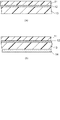
図1(a)あるいは(b)に示されるように、本実施形態の電磁シールド性カバーレイフィルムは、絶縁性樹脂からなるカバーフィルム状基材11と、導電層12と、エラストマーを含有する絶縁性接着層13とがこの順に積層されてなる。
As shown in FIG. 1 (a) or (b), the electromagnetic shielding coverlay film of the present embodiment includes a cover film-
ここで、カバーフィルム状基材11と導電層12とは、導電層12が金属箔である場合、例えばホットメルト接着剤を介してラミネートされる。あるいは、カバーフィルム状基材11と導電層12の間の熱圧着により直接接合する。また、導電層12は、カバーフィルム状基材11の主面に真空蒸着、スパッタリング等のPVD法、CVD法、メッキ法等により成膜され積層した構造になっていてもよい。
Here, when the
そして、絶縁性接着層13は、導電層12において、カバーフィルム状基材11に対向する他方の面に、キャスティング法、熱圧着、貼着等により積層している。ここで、絶縁性接着層13が熱硬化性樹脂からなる場合には、絶縁性接着層13は未硬化状態あるいは半硬化状態になっている。
And the insulating
そして、図1(b)では、絶縁性接着層13の裏面に更に離型材層14が貼り付けられている。
In FIG. 1B, a
カバーフィルム状基材11は、熱硬化性樹脂あるいは熱可塑性樹脂のどちらであってもよい。例えば、液晶ポリマー、ポリイミド(PI)系樹脂、ポリエチレンナフタレート(PEN)系樹脂あるいはこれ等のコンポジット系樹脂が好適な樹脂材料として挙げられる。また、エポキシ系樹脂を使用することもできる。
The cover film-
液晶ポリマーは優れた高周波における伝送特性及びフレキシブル性を奏すること等から好ましい。ここで、液晶ポリマーとしては、例えばキシダール(商品名.Dartco社製)、ベクトラ(商品名.Clanese社製)で代表される多軸配向の熱可塑性ポリマーである。また、他の絶縁性樹脂を添加・配合し変性したものであってもよい。そして、ベクスターFAタイプ(融点285℃)、ベクスターCT−Xタイプ(融点280℃〜335℃)、BIACフィルム(融点335℃)などが例示される。なお、これ等の液晶ポリマーのガラス転移点Tgは205℃〜300℃と高い温度を呈する。 A liquid crystal polymer is preferable because it exhibits excellent high-frequency transmission characteristics and flexibility. Here, the liquid crystal polymer is, for example, a multiaxially oriented thermoplastic polymer represented by xidar (trade name, manufactured by Dartco) or Vectra (trade name, manufactured by Clanese). Further, it may be modified by adding and blending another insulating resin. Examples thereof include Bexter FA type (melting point 285 ° C.), Bexter CT-X type (melting point 280 ° C. to 335 ° C.), BIAC film (melting point 335 ° C.), and the like. In addition, the glass transition point Tg of these liquid crystal polymers exhibits a high temperature of 205 ° C to 300 ° C.
また、PI系樹脂としては、例えばポリイミドフィルム「カプトン」(商品名.東レ・デュポン社製)、オーラム(商品名.三井化学社製)などが例示される。そして、ポリエチレンナフタレート系樹脂としては、例えばテオネックス(商品名.帝人デュポン社製)の熱可塑性樹脂が好適なものとして例示される。 Examples of the PI resin include polyimide film “Kapton” (trade name, manufactured by Toray DuPont) and Aurum (trade name, manufactured by Mitsui Chemicals). And as a polyethylene naphthalate type-resin, the thermoplastic resin of Teonex (brand name. Product made by Teijin DuPont) is illustrated as a suitable thing, for example.
ここで、カバーフィルム状基材11の膜厚は、それが適用されるFPCおよび材質にあわせて適宜に決められ、例えば5μm〜50μm程度に設定される。
Here, the film thickness of the cover film-
導電層12は、金属材料としてアルミニウム、銅、銀、金を挙げることができる。ここで、電磁シールド性カバーレイフィルムが適用されるFPCにおいて、導電層12の接地電位を安定化するために、例えば1μm厚を超える厚膜化が求められる場合には特にアルミニウム金属がよい。その中でも、電磁シールド性カバーレイフィルムおよびFPCを安価にできるアルミニウム箔が好適である。例えば厚膜のアルミニウム箔は、金属板の圧延、電解メッキなどにより低コストに形成できるからである。なお、導電層12の膜厚は、場合によっては1μm以下であっても構わない。
The
絶縁性接着層13は、エラストマー成分を含有する熱硬化性樹脂あるいは熱可塑性樹脂からなる。熱硬化性樹脂としては例えばPI系樹脂、エポキシ系樹脂がある。そして、熱可塑性樹脂としては液晶ポリマー、ポリエチレンナフタレート系樹脂等がある。ここで、その低吸水性あるいは低吸湿性に優れる樹脂が好ましい。このような絶縁性樹脂であると、その誘電特性における経時変化が小さく安定したものになる。また、FPCにおけるベースフィルムおよび回路配線との接着性が安定し優れたものになる。そして、絶縁性接着層13では、熱硬化などで固化した後の弾性率はそのエラストマー成分量により適宜に調整することができる。
The insulating
また、絶縁性接着層13は熱硬化等で固化した後に低誘電性特性を示すものが好ましい。この低誘電性特性においては、周波数1MHzにおける比誘電率が3.5以下になるのが好適である。このような比誘電率であると、FPCにおける例えば数GHz〜数十GHz帯の高速デジタル信号の高速伝送が容易になる。また、低誘電性特性において、上記高周波数帯における誘電正接は0.005以下になるのが好ましい。このような誘電正接であると、数GHz〜数十GHzの高周波数帯の高速デジタル信号におけるFPCの伝送が小さい誘電損失になる。そして、電気信号の高周波特性を損なうことなく高い品質の信号伝送が容易になる。
The insulating
エラストマーには、熱硬化性のものとしてウレタンゴム、シリコーンゴム、不飽和ポリエステル系エラストマーがある。そして、熱可塑性のものとしては、ポリエステル系、ポリアミド系、ポリオレフィン系、ポリスチレン系等のエラストマーが挙げられる。その中で、ポリエステル樹脂、ニトリルゴム(NBR)、スチレンブタジエンゴム(SBR)等の誘電正接が小さい樹脂がエラストマー成分として好適である。そして、固化後の絶縁性接着層13の例えば引張弾性率は100MPa〜1GPa程度の範囲になるように設定される。
Examples of the elastomer include urethane rubber, silicone rubber, and unsaturated polyester elastomer as thermosetting materials. Examples of the thermoplastic material include polyester-based, polyamide-based, polyolefin-based, and polystyrene-based elastomers. Among them, a resin having a small dielectric loss tangent such as polyester resin, nitrile rubber (NBR), styrene butadiene rubber (SBR) is suitable as the elastomer component. For example, the tensile elastic modulus of the insulating
絶縁性接着層13の膜厚は、カバーフィルム状基材11の材質、FPCにおけるベースフィルムの材質、ベースフィルムに形成される回路配線の厚さ等に即して適宜に決められ、例えば10μm〜100μm程度に設定される。
The film thickness of the insulating
このような中で、特に好適な絶縁性接着層13として、オリゴフェニレンエーテルとスチレンブタジエン系のエラストマーを含有する熱硬化性の合成樹脂が挙げられ、例えば、その未硬化状態のフィルムとしてADFLEMA OPE系(商品名.ナミックス社製)が例示される。あるいは、オリゴフェニレンエーテル、スチレンブタジエン系のエラストマーを含む成分を例えばトルエン等の有機溶剤に適度に溶解または分散させ接着剤に調製したものを使用することもできる。
Among these, a particularly preferable insulating
上述したオリゴフェニレンエーテルは、例えばOPE(2官能ポリフェニレンエーテルオリゴマー)ともいわれ、2官能コアの両末端にポリフェニレンエーテルを付与した高分子の構造になっている。ここで、OPEの平均分子量は500〜5000程度であり、好ましくは1000〜3000である。その市販品として、例えば三菱ガス化学(株)社製のOPE2St−1200、OPE2St−2200等がある。なお、上記OPEは、例えば特開2009−161725号公報、特開2011−68713号公報に記載されているビニル化合物をその組成物として作製される。ここで、OPEの誘導体であってもよく、例えばエポキシ誘導体、スチレン誘導体等がある。 The above-described oligophenylene ether is also called, for example, OPE (bifunctional polyphenylene ether oligomer), and has a polymer structure in which polyphenylene ether is added to both ends of the bifunctional core. Here, the average molecular weight of OPE is about 500 to 5000, preferably 1000 to 3000. Examples of such commercially available products include OPE2St-1200 and OPE2St-2200 manufactured by Mitsubishi Gas Chemical Company, Inc. The OPE is produced by using, for example, a vinyl compound described in JP-A Nos. 2009-161725 and 2011-68713 as a composition. Here, it may be a derivative of OPE, such as an epoxy derivative or a styrene derivative.
このオリゴフェニレンエーテルからなる絶縁性接着層13には、その他の成分が含まれていてもよい。例えば、絶縁性接着層13の硬化温度を調整するために、マレイミド系硬化剤、フェノール系硬化剤、アミン系硬化剤等が適度に混合される。あるいは、接着性を調整するために、例えばエポキシ樹脂およびその硬化触媒が添加される。ここで、硬化触媒としては、熱硬化を短時間にするための例えばアミン系硬化触媒、イミダゾール系硬化触媒が用いられる。
The insulating
いずれにしても、絶縁性接着層13は、その硬化温度あるいはガラス転移点Tgが熱可塑性樹脂からなるカバーフィルム状基材11のガラス転移点Tgあるいは融点Tmよりも低い温度となる樹脂からなる。ここで、硬化温度は、その未硬化樹脂フィルムあるいは接着剤層を重合あるいは架橋させて硬化させる温度である。カバーフィルム状基材11の樹脂はガラス転移点を有する場合と明確なTgを示さない場合があるが、明確なTgを示さない場合に絶縁性接着層13の熱硬化温度あるいはTgは熱可塑性樹脂の融点Tmより低くなるようにする。
In any case, the insulating
なお、ガラス転移点は、通常、ガラス転移温度測定方法(JIS C 6493に準ずる)により、TMA法とDMA法の2方法で求められる。ここで、TMA法は、試験片を室温から10℃/分の割合で昇温させ、熱分析装置にて厚さ方向の熱膨張量を測定し、ガラス転移点の前後の曲線に接線を引き、この接線の交点からTgを求める。DMA法(引張り法)は、試験片を室温から2℃/分の割合で昇温させ、粘弾性測定装置にて試験片の動的粘弾性および損失正接を測定し、損失正接のピーク温度からTgを求める。また、弾性率には樹脂フィルムの引張弾性率あるいは曲げ弾性率が用いられる。そして、上記弾性率はJIS K 7127あるいはASTM D 882に準じて測定される。 In addition, a glass transition point is normally calculated | required by two methods, TMA method and DMA method, by the glass transition temperature measuring method (it applies to JISC6493). Here, in the TMA method, the test piece is heated from room temperature at a rate of 10 ° C./min, the amount of thermal expansion in the thickness direction is measured with a thermal analyzer, and a tangent line is drawn on the curves before and after the glass transition point. Tg is obtained from the intersection of the tangent lines. In the DMA method (tensile method), the test piece is heated from room temperature at a rate of 2 ° C./min, the dynamic viscoelasticity and loss tangent of the test piece are measured with a viscoelasticity measuring device, and the peak temperature of the loss tangent is measured. Obtain Tg. As the elastic modulus, the tensile elastic modulus or bending elastic modulus of the resin film is used. The elastic modulus is measured according to JIS K 7127 or ASTM D882.
離型材層14は、絶縁性接着層13の形状を損なうことなく剥離できるものであれば特に限定されない。それを構成する具体的な離型材としては、例えばポリプロピレン(PP)フィルム、ポリエチレン(PE)フィルム、シリコーン離型材付きPPフィルムおよびPEフィルム等が挙げられる。また、例えば上質紙、クラフト紙等の原紙の両面にその吸放湿によるカールを防止するためのプラスチック層を有する離型紙が挙げられる。そのようなものとして、例えばPP樹脂コート紙、PE樹脂コート紙等がある。離型材層13の厚さは、任意の厚さでよいが、樹脂フィルムでは例えば10μm〜50μm、離型紙では例えば50μm〜100μmになる。
The
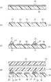
次に、本実施形態の電磁シールド性カバーレイフィルムを用いたフレキシブル配線板およびその製造方法について図2乃至図4を参照して説明する。ここでは高周波信号が伝送される伝送配線が形成されたFPCについて説明される。図2に示すように、その一例のFPCでは、樹脂からなるベースフィルム15の一主面に複数のストリップ線路である内層の信号配線16およびグランド配線17が配線パターンにされ配設されている。ここで、信号配線16はLVDS(Low Voltage Differential Signaling)に対応できる2本ペアの伝送配線として示されている。
Next, a flexible wiring board using the electromagnetic shielding coverlay film of the present embodiment and a manufacturing method thereof will be described with reference to FIGS. Here, an FPC in which transmission wiring for transmitting a high-frequency signal is formed will be described. As shown in FIG. 2, in the FPC as an example, an inner
そして、FPCの表層には、上述したような電磁シールド性カバーレイフィルムが絶縁性接着層13を介して、信号配線16、グランド配線17およびベースフィルム15に熱圧着され接合一体化し形成されている。ここで、グランド配線17の所定の領域に設けられた導通部材18が絶縁性接着層13を貫挿して電磁シールド性カバーレイフィルムの導電層12に電気接続している。
On the surface layer of the FPC, the electromagnetic shielding coverlay film as described above is thermocompression bonded to the
ここで、導電層12が例えばアルミニウム箔、銅箔のように1μmを超える厚さに形成されていると、FPCにおける導電層12およびグランド配線17の接地電位が安定したものになる。そして、信号配線16間のクロストークが安定的に防止される。また、信号配線16の特定インピーダンス、差動インピーダンス等が安定したものになる。また、この導電層12は電磁波シールドとしても機能する。
Here, when the
そして、絶縁性接着層13は、弾性率が小さく、導電層12との界面における強い接着性と共に伸縮性に優れる。また、この絶縁性接着層13は、FPCの信号配線16あるいはグランド配線17のような回路配線と強く接着し、その界面領域でも優れた伸縮性を有する。このため、FPCの折り曲げで生じる導電層12からの応力を吸収し、導電層12からの応力に対する高い緩衝機能を有する。この導電層12からの応力は、その厚さが増えると共に大きくなり、FPCの回路配線の断線を引き起こし易くする。この断線は回路配線の微細化と共に顕著になる。絶縁性接着層13の上述した応力の高い吸収能力がFPCにおける回路配線の断線を防止するように働く。そして、FPCは優れた屈曲特性を有するようになる。
The insulating
上記FPCにおいて、カバーフィルム状基材11とベースフィルム15に上述した液晶ポリマーを用い、絶縁性接着層13にオリゴフェニレンエーテルとスチレンブタジエン系のエラストマーを含有する合成樹脂を用いると好適である。この組み合わせでは、電磁シールド性カバーレイフィルムを構成するカバーフィルム状基材11と絶縁性接着層13およびベースフィルム15の比誘電率は全て3以下になる。また、それ等の誘電正接は0.003以下になる。そして、このFPCにおける信号配線16は、数GHz〜数十GHz帯の高速デジタル信号の極めて優れた伝送特性を示す。
In the FPC, it is preferable to use the above-described liquid crystal polymer for the cover film-
上記FPCでは、ベースフィルム15としては、液晶ポリマーの他に、PI系樹脂、PEN系樹脂あるいはこれ等のコンポジット系樹脂が好適に使用される。あるいは、その他の低誘電性特性を有する熱可塑性樹脂あるいは熱硬化性樹脂を用いることができる。例えば、ポリエチレンテレフタレート(PET)、ポリアミドイミド等がある。
In the FPC, as the
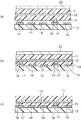
次に、フレキシブル配線板の製造方法の一例について説明する。図3(a)に示すように、例えば厚さが15μm〜50μm程度の液晶ポリマーからなるベースフィルム15の表面に銅箔19が張着された片面銅張積層板を用意する。ここで、銅箔19の厚さは3μm〜35μm程度である。なお、片面銅張積層板は樹脂フィルムの表面に銅箔を熱圧着したものであってもよいし、電解メッキしたものであってもよい。そして、図3(b)に示すように、公知のエッチングにより銅箔19をストリップ線路として配線パターン化する。そして、例えば線幅が20μm〜100μm程度の信号配線16および線幅が200μm〜500μm程度のグランド配線17を形成する。
Next, an example of the manufacturing method of a flexible wiring board is demonstrated. As shown in FIG. 3A, for example, a single-sided copper-clad laminate in which a
次に、図3(c)に示すように、例えば無洗浄タイプのフラックス20が接触塗布されているハンダボール21をグランド配線17の所定領域に載置する。このハンダボール21の載置では、例えば吸引治具の吸引ノズルを減圧吸引し、ハンダボール21の下面にフラックス20を接触塗布する。そして、ハンダボール21を吸引している吸引ノズルをグランド配線17の所定領域にアライメントし吸引を解除して搭載する。
Next, as shown in FIG. 3C, for example, a
ハンダボール21の大きさはグランド配線17の線幅あるいは絶縁性接着層13の厚さにより適宜に決められる。ハンダボール21としては、鉛フリーの共晶ハンダであって例えばSn−Zn系ハンダ、Sn−Bi系ハンダ、Sn−Cu系ハンダ、Sn−Ag系ハンダが好適なものとして挙げられる。ここで、ハンダボール21は、その融点が後述する絶縁性接着層13の軟化又は流動温度よりも高くなり、絶縁性接着層13の硬化温度あるいは融点Tmより低くなるように選択される。絶縁性接着層13がオリゴフェニレンエーテルとスチレンブタジエン系のエラストマーを含有する熱硬化性の合成樹脂である場合には、ハンダボール21はSn−92Znハンダが好適である。
The size of the
次に、例えば厚さが5μm〜50μm程度のPI樹脂からなるカバーフィルム状基材11の表面にアルミニウム箔の導電層12が張着された片面アルミ金属張積層板を用意する。そして、図3(d)に示すように、例えば厚さが15μm〜100μm程度で未硬化フィルム状の絶縁性接着層13と、上述した片面アルミ金属張積層板をベースフィルム15の上方から順に重ね合せてセットアップする。ここで、絶縁性接着層13はオリゴフェニレンエーテルとスチレンブタジエン系のエラストマーを含有する熱硬化性の合成樹脂とする。なお、片面アルミ金属張積層板は、カバーフィルム状基材11に対向する導電層12の他方の面に絶縁性接着層13が接するように重ねられる。
Next, for example, a single-sided aluminum metal-clad laminate in which an aluminum foil
なお、上述した片面アルミ金属張積層板と未硬化フィルム状の絶縁性接着層13の替りに、図1で示したカバーフィルム状基材11、導電層12および絶縁性接着層13から成る電磁シールド性カバーレイフィルムを重ねるようにしてもよい。
In addition, instead of the above-mentioned single-sided aluminum metal-clad laminate and the uncured film-like insulating
そして、図4(a)、図4(b)に示すように、カバーフィルム状基材11上に積層クッションシート22を重ね、公知の加熱加圧処理(熱プレス)により、絶縁性接着層13を介してカバーフィルム状基材11と導電層12をベースフィルム15に接合させる。この熱プレスでは、雰囲気ガスは減圧状態であり、その加熱温度は例えば160℃〜200℃程度になる。そして、その加圧は例えば10〜40kgf/cm2程度である。
Then, as shown in FIGS. 4A and 4B, the
ここで、ハンダボール21は、その融点が198℃程度になるSn−92Znの共晶ハンダからなると、上記熱プレスにおいて、初めは図4(a)に示されるように軟化する絶縁性接着層13を貫挿し、それから導電層12に接するようになる。そして、加熱温度が上昇し絶縁性接着層13が硬化し始めると、ハンダボール21は溶融し、図4(b)に示されるように導通部材18となり導電層12に電気接続するようになる。このようにして、導電層12を有するカバーフィルム状基材11は絶縁性接着層13を介してベースフィルム15、信号配線16およびグランド配線17と接合一体化する。
Here, when the
そして、図4(c)に示すように、積層クッションシート22を剥離する。その後の工程では、加圧することなく所定温度で所定時間の加熱処理を施してもよい。更に、図示しないが、カバーフィルム状基材11、導電層12および絶縁性接着層13からなる電磁シールド性カバーレイフィルムの所定箇所あるいはベースフィルム15の所定箇所を選択的にエッチング除去する。この除去により露出した信号配線16およびグランド配線17にNi、Au等にメッキを施し端子部とする。このようにして図2に示した断面構造のフレキシブル配線板が作製される。
Then, as shown in FIG. 4C, the
絶縁性接着層13はその熱硬化後の弾性率がカバーフィルム状基材11あるいはベースフィルム15の弾性率よりも小さくなり、導電層12、ベースフィルム15、信号配線16、グランド配線17との優れた接合が可能になる。これは、加熱状態から室温へと降温する際に生じる熱応力が絶縁性接着層13により吸収され緩和されるようになるからである。
The insulating
また、熱硬化後の絶縁性接着層13は、その吸湿性が小さく、比誘電率2.4〜3.0および誘電正接0.0015〜0.003の安定した値を示す。また、そのガラス転移点は例えば180℃〜230℃と高い値を呈する。
Moreover, the insulating
また、ベースフィルム15、信号配線16およびグランド配線17との接合において、絶縁性接着層13のしみだし量が従来の接着剤層の場合に較べて大幅に低減するようになる。このため、熱プレス法を用いた接合一体化における作業性が優れたものになる。
Further, in the bonding with the
FPCの製造方法において、絶縁性接着層13としてその他の熱硬化性樹脂であるPI系樹脂あるいはエポキシ系樹脂を母材として使用することができる。但し、上述したようにハンダボール21は、その融点がこれ等の絶縁性接着層13の軟化又は流動温度よりも高くなり、絶縁性接着層13の硬化温度より低くなるように選択される。例えば熱硬化温度が160℃〜170℃程度となる絶縁性接着層13の場合には、ハンダボール21としては低融点ハンダである例えばSn−58Biハンダが好適である。
In the FPC manufacturing method, as the insulating
また、絶縁性接着層13として熱可塑性樹脂を用いる場合には、その融点Tmは、カバーフィルム状基材11あるいはベースフィルム15のガラス転移点Tgより低くなると共に、ハンダボール21の融点より高くなるように選択される。
When a thermoplastic resin is used as the insulating
FPCの製造方法において、導通部材18はハンダボール21の替りに公知の導電性バンプにより形成するようにしてもよい。この場合には、図3(c)の工程において、ハンダボール21の替りに、グランド配線17の所定領域に例えばステンレス鋼製のスクリーン版などを使用し円錐導電性ペーストのバンプ付けをする。ここで、導電性ペーストは、例えば銀、金、銅、錫、鉛、カーボン等の金属粒子とエポキシ樹脂、フェノール樹脂、アクリル樹脂等とを混合したものである。そして、上述したように熱プレスをすると、円錐導電性ペーストは、その頭部が圧潰する塑性変形と共にその組成変化が生じて導電性バンプになる。そして、導電性バンプは絶縁性接着層13を貫挿し導通部材18として導電層12に接続する。
In the FPC manufacturing method, the
上述したグランド配線17を導電層12に電気接続するような場合には、多数の導通部材18は不要であって適当数にあればよい。このため、上記FPCの場合には、導通部材18の形成にハンダボール21を用いるFPCの製造方法はその低コスト化を容易にする。これは、多数の導通部材18を形成する場合に効果的な上記スクリーン印刷を用いた導電性バンプの形成の場合に較べて、ハンダボール21の載置の作業が極めて簡便になるからである。
When the above-described
次に、フレキシブル配線板の他例について図5を参照して説明する。これは2層構造の回路配線が配設されるFPCの場合である。ここでは、高速デジタル信号が伝達される回路配線が形成されたFPCについて説明される。図2で説明したのと同様にベースフィルム15の一主面に信号配線16およびグランド配線17が配設されている。そして、グランド配線17は導通部材18により導電層12に電気接続し、ベースフィルム15の一主面は、カバーフィルム状基材11、導電層12および絶縁性接着層13からなる第1電磁シールド性カバーレイフィルム23により被覆されている。
Next, another example of the flexible wiring board will be described with reference to FIG. This is the case of an FPC in which circuit wiring having a two-layer structure is provided. Here, an FPC in which circuit wiring for transmitting a high-speed digital signal is formed will be described. As described with reference to FIG. 2, the
同様に、ベースフィルム15の他主面に複数の信号配線16aとグランド配線17aが例えば銅箔の別の配線パターンに配設されている。グランド配線17aは導通部材18aにより導電層12aに電気接続している。そして、ベースフィルム15の他主面は第2電磁シールド性カバーレイフィルム23aにより被覆されている。第2電磁シールド性カバーレイフィルム23aは、カバーフィルム状基材11a、導電層12aおよび絶縁性接着層13aからなる。ここで、第2電磁シールド性カバーレイフィルム23aは、第1電磁シールド性カバーレイフィルム23と同一あるいは異なる材料により構成される。
Similarly, a plurality of
上記2層構造のFPCにおいて、絶縁性接着層13,13aにオリゴフェニレンエーテルとスチレンブタジエン系のエラストマーを含有する合成樹脂を用いると好適になる。そして、ベースフィルム15には液晶ポリマーを用いるとよい。この組み合わせでは、図2に示した1層構造のFPCの場合と同様に、このFPCにおける信号配線16,16aは、数GHz〜数十GHz帯の高速デジタル信号の極めて優れた伝送特性を示す。そして、例えばコンピュータのCPUクロックのようにGHz帯に達する高速デジタル信号に対応した配線回路を有するFPCが容易に提供される。
In the FPC having the two-layer structure, it is preferable to use a synthetic resin containing oligophenylene ether and a styrene-butadiene elastomer for the insulating
なお、2層構造FPCにおけるベースフィルム15でも、液晶ポリマーの他に、PI系樹脂、PEN系樹脂あるいはこれ等のコンポジット系樹脂が好適に使用される。あるいは、その他の低誘電性特性を有する熱可塑性樹脂あるいは熱硬化性樹脂を用いることができる。
Note that, in the
上記実施形態では、1層構造あるいは2層構造の配線が形成されるFPCの場合について説明しているが、3層以上の配線を有する多層配線板の場合であっても、同様にFPCの表面に電磁シールド性カバーレイフィルムを形成できる。 In the above embodiment, the case of an FPC in which a wiring having a single layer structure or a two layer structure is formed has been described. Even in the case of a multilayer wiring board having three or more layers of wiring, the surface of the FPC is similarly applied. An electromagnetic shielding coverlay film can be formed.
本実施形態では、電磁シールド性カバーレイフィルムの絶縁性接着層13は、弾性率が小さく調整されて特に引張方向の伸縮性に富む。そして、FPCの折り曲げで生じる導電層12からの応力を吸収し高い緩衝機能を有する。このために、FPCの折り曲げにおいて、FPCの回路配線は導電層12からの応力を受けにくく断線し難くなる。FPCの回路配線に生じる導電層12からの応力は、その厚さが増えると共に増大し、その断線は回路配線の微細化と共に顕著になる。この場合、絶縁性接着層13の上述した応力の高い吸収能力はFPCの折り曲げに対して顕著に働く。そして、FPCは優れた屈曲特性を有するようになる。
In the present embodiment, the insulating
このために、FPCの優れた屈曲特性を維持したままで、導電層12を銅箔にして例えば1μmを超える厚さに形成できる。そして、FPCにおいて接地電位は安定化し、回路配線の特定インピーダンス、差動インピーダンス等は極めて安定したものになる。また、回路配線間のクロストークが安定的に防止できる。同時に、FPCは電磁波シールドされる。
For this reason, the
また、導電層12をアルミニウム箔のようなアルミニウム金属にすることにより、電磁シールド性カバーレイフィルムおよびそれを用いたFPCは安価にできる。更に、FPCにおいて、その回路配線と導電層12とを電気接続する導通部材18としてハンダボールを用いて形成することにより、FPC製造の低コスト化が容易になる。
Moreover, the electromagnetic shielding coverlay film and the FPC using the same can be made inexpensive by making the
本実施形態の電磁シールド性カバーレイフィルムであると、ベースフィルム15および回路配線と電磁シールド性カバーレイフィルムの接合一体化において、従来のように比誘電率および誘電正接を大きくさせる接着剤は使用しなくてもよい。更に、上述したようにベースフィルム15および電磁シールド性カバーレイフィルムの組み合わせにより安定した接着ができる。そして、これ等を接合一体化して作製されるFPCにおける基板材料の比誘電率、およびそれ等の誘電正接を小さくすることが容易になる。そのため、このようなFPCは、高周波信号の高速化、低い誘電損失化が容易であり、その優れた伝送特性を有した高性能なものにできる。
In the case of the electromagnetic shielding coverlay film of the present embodiment, an adhesive that increases the relative dielectric constant and dielectric loss tangent as in the prior art is used in joining and integrating the
更に、絶縁性接着層のガラス転移点は180℃以上にでき、高い耐熱性および高い屈曲耐性を有するFPCが可能になる。そして、例えば自動車のような車載機器への需要に応えることが可能になる。なお、この場合には、カバーフィルム状基材11およびベースフィルム15は、液晶ポリマー、PI系樹脂あるいはPEN系樹脂からなると好適である。
Furthermore, the glass transition point of the insulating adhesive layer can be 180 ° C. or higher, and an FPC having high heat resistance and high bending resistance becomes possible. And it becomes possible to meet the demand for in-vehicle devices such as automobiles. In this case, the cover film-
また、本実施形態で使用される絶縁性接着層は、その組成を調整することによりガラス転移点を230℃以上にすることも可能になる。このために、FPCへの半導体素子等の部品実装において、例えば230℃程度の鉛フリーのハンダリフローを行う厳しい環境下でも耐え得る高耐熱性のFPCが実現できる。 In addition, the insulating adhesive layer used in the present embodiment can have a glass transition point of 230 ° C. or higher by adjusting its composition. For this reason, in mounting components such as semiconductor elements on the FPC, it is possible to realize a high heat resistance FPC that can withstand even a severe environment in which lead-free solder reflow at about 230 ° C. is performed.
次に、実施例により本発明の効果について図6を参照して具体的に説明するが、本発明は下記の実施例に限定されるものではない。 Next, the effects of the present invention will be described in detail with reference to examples, but the present invention is not limited to the following examples.
(実施例1、比較例1)
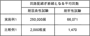
実施形態で説明したフレキシブル配線板の製造方法により、MIT屈曲試験用のFPCサンプル(テストクーポン)を作製した。実施例1のテストクーポンは、幅15mm、長さ220mmのフラットケーブルである。ここで、カバーフィルム状基材11は厚み25μmのポリイミド樹脂からなり、導電層12は厚み9μmのアルミニウム箔からなり、絶縁性接着層13は、厚み50μmのADFLEMA OPE系(商品名.ナミックス社製)樹脂である。また、ベースフィルム15は厚み25μmの液晶ポリマーからなり、その主面に厚み20μm、線幅40μmの断線テスト用の信号配線が配設されている。そして、比較例1では、導電層12が厚み9μmの銅箔である以外は実施例1と同じに構造になっている。
(Example 1, Comparative Example 1)
An FPC sample (test coupon) for the MIT bending test was produced by the method for manufacturing a flexible wiring board described in the embodiment. The test coupon of Example 1 is a flat cable having a width of 15 mm and a length of 220 mm. Here, the cover film-
そして、実施例1および比較例1のFPCの屈曲特性を評価した。ここで、屈曲特性の評価方法はJIS−C5016に準じた耐屈曲性試験および耐折性試験である。それ等の結果が、それぞれ6枚のテストクーポンを試験した場合の平均値として図6にまとめられている。 And the bending characteristic of FPC of Example 1 and Comparative Example 1 was evaluated. Here, the evaluation method of a bending characteristic is a bending resistance test and a bending resistance test according to JIS-C5016. These results are summarized in FIG. 6 as an average value when six test coupons are tested.
耐屈曲性試験はスライド試験であり、折り曲げ外径を6mm(折り曲げ半径3mm×2)とした。スライド条件は、温度を85℃とし、そのストロークを30mm、往復回数を30回/分とした。そして、断線テスト用の信号配線の抵抗値が初期の2倍となるスライド回数を回路配線が断線となる回数にした。 The bending resistance test was a slide test, and the bending outer diameter was 6 mm (folding radius 3 mm × 2). The slide conditions were such that the temperature was 85 ° C., the stroke was 30 mm, and the number of reciprocations was 30 times / minute. Then, the number of times the resistance of the signal wiring for the disconnection test becomes twice the initial value is set to the number of times that the circuit wiring is disconnected.
耐折試験は東洋精機社製MIT屈曲試験機を用いた。ここで、荷重500g、屈折角135°、屈折サイクル175cpm、屈曲部曲率半径3mm、室温(25℃)の条件下で、通電試験により断線テスト用の信号配線の通電状態切れまでの回数を測定した。 For the folding test, an MIT bending tester manufactured by Toyo Seiki Co., Ltd. was used. Here, under the conditions of a load of 500 g, a refraction angle of 135 °, a refraction cycle of 175 cpm, a bending portion curvature radius of 3 mm, and a room temperature (25 ° C.), the number of times until the disconnection test signal wiring was turned off was measured. .
(評価結果)
図6に示すように、実施例1では、耐屈曲性試験が25万回でも全てのサンプルにおいて、その断線テスト用の信号配線の抵抗値に変化はみられなかった。そこで、それ以上のスライド試験は取り止めて25万回超とした。これに対して、比較例1では、1,700回から2,200回でその平均は2,000回程度である。耐屈曲性試験の場合、実施例1は比較例1の少なくとも100倍以上に屈曲特性が向上する。
(Evaluation results)
As shown in FIG. 6, in Example 1, the resistance value of the signal wiring for the disconnection test was not changed in all the samples even when the bending resistance test was 250,000 times. Therefore, the further slide test was canceled and exceeded 250,000 times. On the other hand, in the comparative example 1, the average is about 2,000 times from 1,700 times to 2,200 times. In the case of the bending resistance test, the bending property of Example 1 is improved at least 100 times that of Comparative Example 1.
また、実施例1では、耐折性試験が51,728回から91,348回で平均値は66,071回となった。これに対して、比較例1では、963回から2,299回でその平均は1,470回である。耐折性試験の場合、実施例1は比較例1の約50倍程度に屈曲特性が向上する。 In Example 1, the folding resistance test was 51,728 times to 91,348 times, and the average value was 66,071 times. On the other hand, in the comparative example 1, the average is 1,470 times from 963 times to 2,299 times. In the case of the bending resistance test, the bending property of Example 1 is improved to about 50 times that of Comparative Example 1.
これ等の結果から、電磁シールド性カバーレイフィルムにおいて、導電層12が厚膜化する場合、アルミニウム箔は銅箔よりもFPCの屈曲特性を大幅に向上させ、特に厚膜の導電層12の場合に好適になることが確認された。
From these results, in the electromagnetic shielding coverlay film, when the
以上、本発明の好適な実施形態について説明したが、上述した実施形態は本発明を限定するものでない。当業者にあっては、具体的な実施態様において本発明の技術思想および技術範囲から逸脱せずに種々の変形・変更を加えることが可能である。 Although the preferred embodiments of the present invention have been described above, the above-described embodiments do not limit the present invention. Those skilled in the art can make various modifications and changes in specific embodiments without departing from the technical idea and technical scope of the present invention.
例えば、本実施形態で説明した電磁シールド性カバーレイフィルムは、フレキシブル配線板の他にも、例えばリジッド配線板に対してその表面を被覆し一体接合するように適用される。但し、この場合には、電磁シールド性カバーレイフィルムの優れた屈曲特性は余り活かされない。 For example, the electromagnetic shielding coverlay film described in the present embodiment is applied so as to cover and integrally bond the surface of a rigid wiring board in addition to a flexible wiring board, for example. However, in this case, the excellent bending characteristics of the electromagnetic shielding coverlay film are not utilized much.
本発明は、本実施形態で説明したような高周波信号が伝送されるフレキシブル配線板の場合に限定されるものでない。例えば1MHz未満になる低周波の電気信号が伝送されるFPCの場合であっても同様に有効になることに言及しておく。 The present invention is not limited to a flexible wiring board that transmits a high-frequency signal as described in the present embodiment. For example, it should be noted that the present invention is similarly effective even in the case of an FPC that transmits a low-frequency electrical signal of less than 1 MHz.
11,11a…カバーフィルム状基材、12,12a…導電層、13,13a…絶縁性接着層、14…離型材層、15…ベースフィルム、16,16a…信号配線、17,17a…グランド配線、18,18a…導通部材、19…銅箔、20…フラックス、21…ハンダボール、22…積層クッションシート、23…第1電磁シールド性カバーレイフィルム、23a…第2電磁シールド性カバーレイフィルム
DESCRIPTION OF
ところで、データ処理が高速化する半導体デバイスのような電子部品が搭載される電子機器では、その小型化と共に動作周波数の高周波化が進む。そのため、FPCは、高周波信号における、安定したインピーダンスおよび低い伝送損失による優れた電気信号の伝送特性が求められる。例えば電気信号の周波数が数GHz〜数十GHz帯の高速デジタル信号の使用において、その周波数特性を損なうことなく高速伝送することが要求される。そのため、例えば画質が高精細化した画像を伝送するような電子機器に用いられるFPCの場合、その特定インピーダンスあるいは差動インピーダンスの安定化が強く求められる。 By the way, in an electronic device in which an electronic component such as a semiconductor device that speeds up data processing is mounted, the operating frequency increases with the miniaturization. Therefore, the FPC is required to have excellent electrical signal transmission characteristics due to stable impedance and low transmission loss in high-frequency signals. For example, when a high-speed digital signal having a frequency of an electrical signal of several GHz to several tens of GHz is used, high-speed transmission is required without impairing the frequency characteristics . Therefore, for example, in the case of an FPC used in an electronic device that transmits an image with high definition, stabilization of the specific impedance or differential impedance is strongly required.
ここで、導電層12が例えばアルミニウム箔、銅箔のように1μmを超える厚さに形成されていると、FPCにおける導電層12およびグランド配線17の接地電位が安定したものになる。そして、信号配線16間のクロストークが安定的に防止される。また、信号配線16の特性インピーダンス、差動インピーダンス等が安定したものになる。また、この導電層12は電磁波シールドとしても機能する。
Here, when the
このために、FPCの優れた屈曲特性を維持したままで、導電層12を銅箔にして例えば1μmを超える厚さに形成できる。そして、FPCにおいて接地電位は安定化し、回路配線の特性インピーダンス、差動インピーダンス等は極めて安定したものになる。また、回路配線間のクロストークが安定的に防止できる。同時に、FPCは電磁波シールドされる。
For this reason, the
Claims (7)
Priority Applications (1)
| Application Number | Priority Date | Filing Date | Title |
|---|---|---|---|
| JP2012060238A JP2013193253A (en) | 2012-03-16 | 2012-03-16 | Electromagnetic shielding coverlay film, flexible wiring board and method for manufacturing the same |
Applications Claiming Priority (1)
| Application Number | Priority Date | Filing Date | Title |
|---|---|---|---|
| JP2012060238A JP2013193253A (en) | 2012-03-16 | 2012-03-16 | Electromagnetic shielding coverlay film, flexible wiring board and method for manufacturing the same |
Publications (1)
| Publication Number | Publication Date |
|---|---|
| JP2013193253A true JP2013193253A (en) | 2013-09-30 |
Family
ID=49392808
Family Applications (1)
| Application Number | Title | Priority Date | Filing Date |
|---|---|---|---|
| JP2012060238A Pending JP2013193253A (en) | 2012-03-16 | 2012-03-16 | Electromagnetic shielding coverlay film, flexible wiring board and method for manufacturing the same |
Country Status (1)
| Country | Link |
|---|---|
| JP (1) | JP2013193253A (en) |
Cited By (14)
| Publication number | Priority date | Publication date | Assignee | Title |
|---|---|---|---|---|
| JP2015133474A (en) * | 2014-01-14 | 2015-07-23 | 広州方邦電子有限公司 | Electromagnetic shield film and method of manufacturing circuit board including shield film |
| JP5861790B1 (en) * | 2015-02-25 | 2016-02-16 | 東洋インキScホールディングス株式会社 | Electromagnetic shielding sheet, electromagnetic shielding wiring circuit board, and electronic equipment |
| JP2017092416A (en) * | 2015-11-17 | 2017-05-25 | 信越ポリマー株式会社 | Electromagnetic wave shield film and electromagnetic wave shield film-attached printed wiring board |
| JP2017188307A (en) * | 2016-04-05 | 2017-10-12 | 住友電気工業株式会社 | Shielded flexible flat cable, and manufacturing method of shielded flexible flat cable |
| CN108156750A (en) * | 2018-01-11 | 2018-06-12 | 深圳市景旺电子股份有限公司 | A kind of flexible PCB and preparation method thereof |
| CN109892020A (en) * | 2017-02-13 | 2019-06-14 | 拓自达电线株式会社 | Earthing component, shielding printed wiring board and the manufacturing method for shielding printed wiring board |
| CN110278701A (en) * | 2018-03-15 | 2019-09-24 | 拓自达电线株式会社 | Electromagnetic shielding film and shielding printed wiring board |
| WO2020090726A1 (en) * | 2018-10-29 | 2020-05-07 | タツタ電線株式会社 | Electromagnetic shielding film, method for producing shielded printed wiring board, and shielded printed wiring board |
| JP2020205433A (en) * | 2020-08-25 | 2020-12-24 | 東洋インキScホールディングス株式会社 | Flexible printed wiring board, manufacturing method of the flexible printed wiring board, and electron member |
| JP2021052063A (en) * | 2019-09-24 | 2021-04-01 | 信越ポリマー株式会社 | Coverlay film with electromagnetic wave shield and method for manufacturing the same, and flexible printed wiring board with electromagnetic wave shield and method for manufacturing the same |
| JPWO2020090727A1 (en) * | 2018-10-29 | 2021-10-21 | タツタ電線株式会社 | Electromagnetic wave shield film, shield print wiring board manufacturing method, and shield print wiring board |
| CN113692110A (en) * | 2021-08-10 | 2021-11-23 | Oppo广东移动通信有限公司 | Flexible circuit board and mobile terminal |
| CN114293164A (en) * | 2021-12-29 | 2022-04-08 | 立芯科技(昆山)有限公司 | Preparation method of electromagnetic shielding layer of semiconductor product and semiconductor product |
| WO2023282318A1 (en) * | 2021-07-09 | 2023-01-12 | 東洋紡株式会社 | Adhesive composition, adhesive sheet, electromagnetic-wave shielding material, laminate, and printed wiring board |
Citations (4)
| Publication number | Priority date | Publication date | Assignee | Title |
|---|---|---|---|---|
| JP2002361770A (en) * | 2001-06-11 | 2002-12-18 | Toray Ind Inc | Cover lay film |
| JP2009278048A (en) * | 2008-05-19 | 2009-11-26 | Kyocera Chemical Corp | Method for producing shield-coating flexible printed wiring board |
| JP2010238870A (en) * | 2009-03-31 | 2010-10-21 | Toyo Ink Mfg Co Ltd | Electromagnetic wave shielding coverlay film, method of manufacturing flexible printed wiring board, and flexible printed wiring board |
| JP2011040493A (en) * | 2009-08-07 | 2011-02-24 | Namics Corp | Multilayered wiring board, and method for manufacturing multilayered wiring board |
-
2012
- 2012-03-16 JP JP2012060238A patent/JP2013193253A/en active Pending
Patent Citations (4)
| Publication number | Priority date | Publication date | Assignee | Title |
|---|---|---|---|---|
| JP2002361770A (en) * | 2001-06-11 | 2002-12-18 | Toray Ind Inc | Cover lay film |
| JP2009278048A (en) * | 2008-05-19 | 2009-11-26 | Kyocera Chemical Corp | Method for producing shield-coating flexible printed wiring board |
| JP2010238870A (en) * | 2009-03-31 | 2010-10-21 | Toyo Ink Mfg Co Ltd | Electromagnetic wave shielding coverlay film, method of manufacturing flexible printed wiring board, and flexible printed wiring board |
| JP2011040493A (en) * | 2009-08-07 | 2011-02-24 | Namics Corp | Multilayered wiring board, and method for manufacturing multilayered wiring board |
Cited By (25)
| Publication number | Priority date | Publication date | Assignee | Title |
|---|---|---|---|---|
| JP2015133474A (en) * | 2014-01-14 | 2015-07-23 | 広州方邦電子有限公司 | Electromagnetic shield film and method of manufacturing circuit board including shield film |
| JP5861790B1 (en) * | 2015-02-25 | 2016-02-16 | 東洋インキScホールディングス株式会社 | Electromagnetic shielding sheet, electromagnetic shielding wiring circuit board, and electronic equipment |
| JP2016157838A (en) * | 2015-02-25 | 2016-09-01 | 東洋インキScホールディングス株式会社 | Electromagnetic wave shielding sheet, electromagnetic wave shielding wiring circuit board, and electronic device |
| JP2017092416A (en) * | 2015-11-17 | 2017-05-25 | 信越ポリマー株式会社 | Electromagnetic wave shield film and electromagnetic wave shield film-attached printed wiring board |
| JP2017188307A (en) * | 2016-04-05 | 2017-10-12 | 住友電気工業株式会社 | Shielded flexible flat cable, and manufacturing method of shielded flexible flat cable |
| CN109892020A (en) * | 2017-02-13 | 2019-06-14 | 拓自达电线株式会社 | Earthing component, shielding printed wiring board and the manufacturing method for shielding printed wiring board |
| CN109892020B (en) * | 2017-02-13 | 2022-03-04 | 拓自达电线株式会社 | Grounding member, shielded printed wiring board, and method for manufacturing shielded printed wiring board |
| CN108156750A (en) * | 2018-01-11 | 2018-06-12 | 深圳市景旺电子股份有限公司 | A kind of flexible PCB and preparation method thereof |
| CN110278701A (en) * | 2018-03-15 | 2019-09-24 | 拓自达电线株式会社 | Electromagnetic shielding film and shielding printed wiring board |
| KR20190109302A (en) * | 2018-03-15 | 2019-09-25 | 타츠타 전선 주식회사 | Electromagnetic wave shield film and shield printed circuit board |
| TWI720356B (en) * | 2018-03-15 | 2021-03-01 | 日商拓自達電線股份有限公司 | Electromagnetic wave shield film and shield printed circuit board |
| KR102423541B1 (en) * | 2018-03-15 | 2022-07-20 | 타츠타 전선 주식회사 | Electromagnetic wave shield film and shield printed circuit board |
| WO2020090726A1 (en) * | 2018-10-29 | 2020-05-07 | タツタ電線株式会社 | Electromagnetic shielding film, method for producing shielded printed wiring board, and shielded printed wiring board |
| JP7244535B2 (en) | 2018-10-29 | 2023-03-22 | タツタ電線株式会社 | EMI SHIELDING FILM, METHOD FOR MANUFACTURING SHIELD PRINTED WIRING BOARD, AND SHIELD PRINTED WIRING BOARD |
| JP7244534B2 (en) | 2018-10-29 | 2023-03-22 | タツタ電線株式会社 | EMI SHIELDING FILM, METHOD FOR MANUFACTURING SHIELD PRINTED WIRING BOARD, AND SHIELD PRINTED WIRING BOARD |
| JPWO2020090727A1 (en) * | 2018-10-29 | 2021-10-21 | タツタ電線株式会社 | Electromagnetic wave shield film, shield print wiring board manufacturing method, and shield print wiring board |
| JPWO2020090726A1 (en) * | 2018-10-29 | 2021-11-11 | タツタ電線株式会社 | Electromagnetic wave shield film, shield print wiring board manufacturing method, and shield print wiring board |
| JP2021052063A (en) * | 2019-09-24 | 2021-04-01 | 信越ポリマー株式会社 | Coverlay film with electromagnetic wave shield and method for manufacturing the same, and flexible printed wiring board with electromagnetic wave shield and method for manufacturing the same |
| CN112638142A (en) * | 2019-09-24 | 2021-04-09 | 信越聚合物株式会社 | Cover film with electromagnetic wave shield and method for manufacturing the same, and flexible printed wiring board with electromagnetic wave shield and method for manufacturing the same |
| JP2020205433A (en) * | 2020-08-25 | 2020-12-24 | 東洋インキScホールディングス株式会社 | Flexible printed wiring board, manufacturing method of the flexible printed wiring board, and electron member |
| WO2023282318A1 (en) * | 2021-07-09 | 2023-01-12 | 東洋紡株式会社 | Adhesive composition, adhesive sheet, electromagnetic-wave shielding material, laminate, and printed wiring board |
| JP7409568B2 (en) | 2021-07-09 | 2024-01-09 | 東洋紡エムシー株式会社 | Adhesive compositions, adhesive sheets, electromagnetic shielding materials, laminates and printed wiring boards |
| CN113692110A (en) * | 2021-08-10 | 2021-11-23 | Oppo广东移动通信有限公司 | Flexible circuit board and mobile terminal |
| CN114293164A (en) * | 2021-12-29 | 2022-04-08 | 立芯科技(昆山)有限公司 | Preparation method of electromagnetic shielding layer of semiconductor product and semiconductor product |
| CN114293164B (en) * | 2021-12-29 | 2024-04-12 | 立芯科技(昆山)有限公司 | Preparation method of electromagnetic shielding layer of semiconductor product and semiconductor product |
Similar Documents
| Publication | Publication Date | Title |
|---|---|---|
| JP2013193253A (en) | Electromagnetic shielding coverlay film, flexible wiring board and method for manufacturing the same | |
| JP5541122B2 (en) | Flexible wiring board | |
| JP3491595B2 (en) | Anisotropic conductive adhesive film | |
| JP4319167B2 (en) | Shield film, shield printed wiring board, shield flexible printed wiring board, shield film manufacturing method, and shield printed wiring board manufacturing method | |
| WO2013099172A1 (en) | Cover lay film, flexible wiring board, and manufacturing method thereof | |
| KR101607552B1 (en) | Electromagnetic-wave shielding material, and printed-wiring board | |
| JP6435540B2 (en) | Electromagnetic wave shielding film, flexible printed wiring board with electromagnetic wave shielding film, and manufacturing method thereof | |
| TWI732995B (en) | Shielded printed wiring board and manufacturing method of shielded printed wiring board | |
| TWI761781B (en) | Grounding member, shielded printed wiring board, and manufacturing method of shielded printed wiring board | |
| JP4397941B2 (en) | Shield film, shield printed wiring board, shield flexible printed wiring board, shield film manufacturing method, and shield printed wiring board manufacturing method | |
| JP6372122B2 (en) | Manufacturing method of electronic equipment | |
| JP6187568B2 (en) | Laminated body for electromagnetic wave shield, electromagnetic wave shield laminated body, electronic device and manufacturing method thereof | |
| JP2014112576A (en) | Shield film | |
| CN107791641B (en) | High-shielding electromagnetic interference shielding film with double metal layers and preparation method thereof | |
| JP6194939B2 (en) | Laminated body for electromagnetic wave shield, electromagnetic wave shield laminated body, electronic device and manufacturing method thereof | |
| JP2018041953A (en) | Electromagnetic wave shield laminate, and electronic apparatus and method for manufacturing the same using the electromagnetic wave shield laminate | |
| TWI602478B (en) | Shape retaining film and shape retaining flexible wiring board containing the shape retaining film | |
| JP2014207297A (en) | Flexible printed circuit, and method for manufacturing the same | |
| JP2013149808A (en) | Metal core flexible wiring board and manufacturing method of the same | |
| WO2021167047A1 (en) | Electroconductive adhesive, electromagnetic shielding film and electroconductive bonding film | |
| JP6180499B2 (en) | Shield film, shield printed wiring board, and method for manufacturing shield printed wiring board | |
| CN106852014A (en) | A kind of novel bonding structure and adhering method | |
| JP2013098296A (en) | Method for manufacturing long flexible wiring board | |
| WO2022131183A1 (en) | Electromagnetic wave shielding film and shielded printed wiring board | |
| JP6180500B2 (en) | Shield film, shield printed wiring board, and method for manufacturing shield printed wiring board |
Legal Events
| Date | Code | Title | Description |
|---|---|---|---|
| A621 | Written request for application examination |
Free format text: JAPANESE INTERMEDIATE CODE: A621 Effective date: 20150204 |
|
| A977 | Report on retrieval |
Free format text: JAPANESE INTERMEDIATE CODE: A971007 Effective date: 20151119 |
|
| A131 | Notification of reasons for refusal |
Free format text: JAPANESE INTERMEDIATE CODE: A131 Effective date: 20151201 |
|
| A02 | Decision of refusal |
Free format text: JAPANESE INTERMEDIATE CODE: A02 Effective date: 20160329 |