JP2013120155A - Gas component detector - Google Patents
Gas component detector Download PDFInfo
- Publication number
- JP2013120155A JP2013120155A JP2011269152A JP2011269152A JP2013120155A JP 2013120155 A JP2013120155 A JP 2013120155A JP 2011269152 A JP2011269152 A JP 2011269152A JP 2011269152 A JP2011269152 A JP 2011269152A JP 2013120155 A JP2013120155 A JP 2013120155A
- Authority
- JP
- Japan
- Prior art keywords
- gas component
- infrared
- component detection
- optical block
- light receiving
- Prior art date
- Legal status (The legal status is an assumption and is not a legal conclusion. Google has not performed a legal analysis and makes no representation as to the accuracy of the status listed.)
- Pending
Links
Images


Abstract
Description
本発明は、赤外線の吸収特性を利用して気体成分の濃度を検出する気体成分検出装置に関する。 The present invention relates to a gas component detection device that detects the concentration of a gas component using infrared absorption characteristics.
従来の気体成分検出装置として、例えば、特許文献1に記載されている赤外線検知式ガスセンサがある。この従来例は、被測定ガスが流入する筒状のケースと、赤外線を放射する光源と、赤外線を集光するコリメータレンズと、赤外線の特定の波長のみを透過するバンドバスフィルタと、前記特定波長の赤外線を電気信号に変換する検出素子とを備える。そして、光源から放射される赤外線のうちで被測定ガス(例えば、二酸化炭素)に吸収されずに検出素子で受光される赤外線の量(レベル)に応じて、ケース内に存在する被測定ガス(検出対象の気体成分)の濃度を検出することができる。
As a conventional gas component detection device, for example, there is an infrared detection type gas sensor described in
ところで、気体成分検出装置を小型化するに当たり、光源(発光素子)や受光素子を信号処理回路とともにパッケージに収納し、検出対象の気体が導入され且つ赤外線の光路となる空間を形成する光学ブロックがパッケージに積載される構造が考えられる。このような構造においては、前記空間の壁面にめっき加工による反射面が形成された光学ブロックが用いられることがある。 By the way, when downsizing the gas component detection device, an optical block that houses a light source (light emitting element) and a light receiving element together with a signal processing circuit in a package and forms a space where a gas to be detected is introduced and becomes an infrared optical path is provided. A structure loaded on a package is conceivable. In such a structure, an optical block having a reflective surface formed by plating on the wall surface of the space may be used.
しかしながら、現在のめっき加工技術ではめっき加工が可能な合成樹脂材料の種類が限られており、特に、リフロー実装時の高温度(はんだの溶融温度である約180℃〜220℃)などに耐え得る合成樹脂材料は種類が少なく且つ高価なものが多い。故に、合成樹脂製の光学ブロックを使用した気体成分検出装置は、コストの上昇を抑えつつ耐熱性の向上を図ることが困難であった。 However, with the current plating technology, the types of synthetic resin materials that can be plated are limited, and in particular, they can withstand high temperatures during reflow mounting (solder melting temperature of about 180 ° C to 220 ° C). There are few kinds of synthetic resin materials and many expensive ones. Therefore, it is difficult for the gas component detection device using the synthetic resin optical block to improve heat resistance while suppressing an increase in cost.
本発明は、上記課題に鑑みて為されたものであり、コストの上昇を抑えつつ耐熱性の向上を図ることを目的とする。 The present invention has been made in view of the above problems, and an object thereof is to improve heat resistance while suppressing an increase in cost.
本発明の気体成分検出装置は、検出対象の気体が導入され且つ赤外線の光路となる空間を形成する光学ブロックと、前記空間内に赤外線を放射する赤外線放射素子、前記光路を進行した後に前記空間外に放射される赤外線を受光し且つ電気信号に変換する受光素子、前記赤外線放射素子を駆動し、且つ前記受光素子から出力される前記電気信号を信号処理する信号処理回路がパッケージ内に収納されてなる回路ブロックとを備え、前記パッケージは、前記信号処理回路と電気的に接続された複数の端子を有し、前記光学ブロックは、金属材料で形成されることを特徴とする。 The gas component detection apparatus according to the present invention includes an optical block that forms a space where a gas to be detected is introduced and serves as an infrared light path, an infrared radiation element that emits infrared light into the space, and the space after traveling through the light path. A light receiving element that receives infrared rays emitted to the outside and converts them into electrical signals, and a signal processing circuit that drives the infrared radiation elements and that processes the electrical signals output from the light receiving elements are housed in a package. The package has a plurality of terminals electrically connected to the signal processing circuit, and the optical block is made of a metal material.
この気体成分検出装置において、前記赤外線放射素子から放射される赤外線を集光する第1集光レンズ、または前記空間を進行して来た赤外線を集光する第2集光レンズの少なくとも何れか一方を備えることが好ましい。 In this gas component detection device, at least one of a first condenser lens that collects infrared rays emitted from the infrared radiation element and a second condenser lens that collects infrared rays that have traveled through the space. It is preferable to provide.
この気体成分検出装置において、前記第2集光レンズは、前記検出対象の気体成分に吸収される波長帯域を通過域に含む波長フィルタが一体に形成されていることが好ましい。 In this gas component detection device, it is preferable that the second condenser lens is integrally formed with a wavelength filter including a wavelength band absorbed by the gas component to be detected in a pass band.
この気体成分検出装置において、前記パッケージは、前記赤外線放射素子から放射される赤外線を前記空間に向けて反射させる第1反射部、または前記空間を進行して来た赤外線を前記受光素子に向けて反射させる第2反射部の少なくとも何れか一方が一体に形成された立体成形回路基板からなることが好ましい。 In this gas component detection device, the package has a first reflecting portion that reflects the infrared rays radiated from the infrared radiation element toward the space, or the infrared rays that have traveled through the space are directed toward the light receiving element. It is preferable that the second reflecting portion to be reflected is formed of a three-dimensional molded circuit board integrally formed.
この気体成分検出装置において、前記赤外線放射素子又は前記受光素子の少なくとも何れか一方は、前記光学ブロックの赤外線の入射面の法線方向又は前記光学ブロックの赤外線の出射面の法線方向と、赤外線の放射面の法線方向又は赤外線の受光面の法線方向とのなす角が鋭角となる向きに配置されることが好ましい。 In this gas component detection device, at least one of the infrared radiation element and the light receiving element includes a normal direction of an infrared incident surface of the optical block or a normal direction of an infrared emission surface of the optical block and an infrared ray. It is preferable that the angle formed by the normal direction of the emission surface or the normal direction of the infrared light receiving surface is arranged in an acute angle.
この気体成分検出装置において、互いに異なる気体成分に吸収される波長帯域を通過域に含む複数の波長フィルタと、前記各波長フィルタを通過する赤外線を受光する複数の前記受光素子とを備えることが好ましい。 The gas component detection device preferably includes a plurality of wavelength filters that include in their passbands wavelength bands that are absorbed by different gas components, and a plurality of the light receiving elements that receive infrared rays that pass through the wavelength filters. .
この気体成分検出装置において、前記光学ブロックは、前記回路ブロックに対向する面が開放された凹所を有する本体と、前記本体に取り付けられて前記凹所の一部を閉塞するカバーとを有することが好ましい。 In this gas component detection device, the optical block has a main body having a recess whose surface facing the circuit block is open, and a cover that is attached to the main body and closes a part of the recess. Is preferred.
この気体成分検出装置において、前記検出対象の気体成分に吸収される波長帯域を通過域に含む波長フィルタを備え、前記光学ブロックは、前記波長フィルタが外部から挿入される挿入口が設けられていることが好ましい。 The gas component detection device includes a wavelength filter including a wavelength band absorbed by the gas component to be detected in a pass band, and the optical block is provided with an insertion port into which the wavelength filter is inserted from the outside. It is preferable.
この気体成分検出装置において、前記光学ブロックは、複数の前記端子のうちで前記信号処理回路のグランド用の端子に接触導通する導通部を有することが好ましい。 In this gas component detection device, it is preferable that the optical block has a conduction portion that is in contact with and connected to a ground terminal of the signal processing circuit among the plurality of terminals.
本発明の気体成分検出装置は、コストの上昇を抑えつつ耐熱性の向上を図ることができるという効果がある。 The gas component detection device of the present invention has an effect that heat resistance can be improved while suppressing an increase in cost.
(実施形態1)
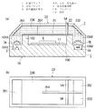
本実施形態の気体成分検出装置(以下、ガスセンサと呼ぶ。)は、図2に示すように回路ブロック1と光学ブロック2で構成されている。なお、以下の説明では、図2において上下左右前後を規定する。
(Embodiment 1)
A gas component detection device (hereinafter referred to as a gas sensor) of this embodiment is composed of a
回路ブロック1は、合成樹脂成形体からなるパッケージ10の内部に赤外線放射素子3、2つの受光素子4A,4B、3つの集光レンズ7A,7B、信号処理回路6を実装した配線板11などが収納されて構成される。赤外線放射素子3は、赤外線を放射する半導体ベアチップ(例えば、発光ダイオードチップや半導体基板上にMEMS技術を用いた抵抗素子が形成されてなる光源)からなる。ただし、赤外線放射素子3から放射される赤外線の波長は、検出対象の気体成分(例えば、一酸化炭素や二酸化炭素、メタン、窒素酸化物など)に吸収され易い波長である。また受光素子4A,4Bは、赤外線を受光して電気信号に変換する半導体ベアチップ(例えば、フォトダイオードチップや焦電素子)からなる。信号処理回路6は、赤外線放射素子3を駆動して赤外線を放射させたり、受光素子4A,4Bから出力される信号に対して増幅や波形整形、サンプリング、A/D変換、演算処理、補正処理、異常濃度判定処理などの信号処理を行う集積回路(IC)からなる。
The
配線板11は矩形平板状に形成されており、ほぼ中央に信号処理回路6が実装され、図示しないプリント配線が上面に形成され、信号処理回路6の端子(図示せず)がプリント配線に電気的に接続されている。
The
パッケージ10は、扁平な直方体形状に形成されるとともに上面側に開口する凹所100が設けられ、この凹所100内に配線板11を収納する。また、パッケージ10の上面側における左端部には、深さ寸法及び前後左右の寸法が異なる2つの凹部101A,101Bが上下方向に重なるように形成されている。そして、深い方の凹部101Aの底面(下面)に赤外線放射素子3が実装され、浅い方の凹部101Bの底面(下面)に第1集光レンズ7Aが載置される(図1(a)参照)。赤外線放射素子3は、ワイヤボンディングなどの適宜の方法により、配線板11のプリント配線と電気的に接続される。また第1集光レンズ7Aは、例えば、シリコン基板を半導体の微細加工技術により加工して形成され、赤外線放射素子3から放射される赤外線を略平行光に集光する。なお、凹部101A,101Bの右端にはパッケージ10の上面とほぼ同じ高さの壁102が設けられている。つまり、赤外線放射素子3から放射される赤外線が壁102で遮蔽されることにより、赤外線が照射されることに起因した信号処理回路6の誤動作を抑制することができる。しかも、このような壁102がパッケージ10と一体に形成されているため、壁がパッケージ10と別体に形成される場合と比較して低コスト化及び小型化が図れるという利点がある。
The
一方、パッケージ10の上面側における右端部には、深さ寸法及び前後左右の寸法が異なる2組の凹部104A,104Bが上下方向に重なるように形成されている。そして、深い方の2つの凹部104Aの底面(下面)にそれぞれ受光素子4A,4Bが実装され、浅い方の2つの凹部104Bの底面(下面)にそれぞれ第2集光レンズ7Bが載置される(図1(a)参照)。なお、受光素子4A,4Bは、ワイヤボンディングなどの適宜の方法により、配線板11のプリント配線と電気的に接続される。また第2集光レンズ7Bは、例えば、シリコン基板を半導体の微細加工技術により加工して形成され、受光素子4A,4Bの受光面に赤外線を集光する。
On the other hand, at the right end portion on the upper surface side of the
パッケージ10の前後両側面には、図2に示すように複数(図示例では4つ)の端子12が左右方向に並んで突出している。これらの端子12は金属板からなり、パッケージ10にインサート成形され、パッケージ10内で配線板11のプリント配線と電気的に接続される。
As shown in FIG. 2, a plurality (four in the illustrated example) of
光学ブロック2は、回路ブロック1に対向する面(下面)が開放された凹所200を有する本体20と、本体20に取り付けられて凹所200の一部を閉塞するカバー21とを有する。本体20は、金属材料(例えば、アルミニウム、真鍮、銅などの板金)により、前後左右の長さ寸法がパッケージ10と等しい略角錐台形状に形成されている。また、本体20上部の中央には、上下方向に貫通する矩形の通気孔(図示せず)が設けられ、通気孔を通して外気(検出対象の気体成分を含む複数種類の混合気体。以下、同じ。)が凹所(空間)200内に導入される。なお、通気孔の形状は矩形に限定されず、円形等の他の形状であってもよく、且つ複数個であってもよい。ただし、塵埃などの外気以外の異物が通気孔に進入することを防ぐため、本体20上面の通気孔の開口は防塵フィルタ24で覆われている(図2参照)。
The
凹所200は、底面(上面)における前後方向の中央に分岐部204が下向きに突設されている。この分岐部204は、薄板状の壁からなり、上下方向から見たときに、後端(右端)が2つの受光素子4A,4Bの間に位置している。また、凹所200の側面並びに底面(上面)、分岐部204の表面は、金などの反射率が相対的に高い金属によってめっきされている。なお、以下では、赤外線放射素子3と対向する左側面を第1反射面201、受光素子4Aと対向する右側面を第2反射面202、受光素子4Bと対向する右側面を第3反射面203と呼ぶ。
In the
カバー21は、本体20と同じ金属材料によって矩形平板状に形成され、本体20の下面側に接合されて凹所200の開口面(下面)の一部(凹部101B,104Bと対向しない部分)を閉塞する。
The
また、分岐部204で分岐された各光路(第1反射面201から第2反射面202と第3反射面203に向かう2つの光路)の途中に主波長フィルタ5A及び副波長フィルタ5Bがそれぞれ配設される(図1(b)参照)。すなわち、一方の光路(主光路)を進行した赤外線が主波長フィルタ5Aを通過し且つ第2反射面202に反射されて受光素子4Aに受光され、他方の光路(副光路)を進行した赤外線が副波長フィルタ5Bを通過し且つ第3反射面203に反射されて受光素子4Bに受光される。ここで、主波長フィルタ5Aは、検出対象の気体成分が吸収する赤外線の波長域を通過域に含むバンドパスフィルタからなる。また、副波長フィルタ5Bは、検出対象の気体成分が吸収する赤外線の波長域を通過域に含まず、当該波長域の近傍の波長域を通過域に含むバンドパスフィルタからなる。この種のバンドパスフィルタは干渉フィルタとも呼ばれ、主に誘電体膜の多層構造を有している。
In addition, the
つまり、赤外線放射素子3から放射される赤外線のうち、主波長フィルタ5Aを通過して受光素子4Aで受光される赤外線量が検出対象の気体成分の濃度(以下、気体濃度という。)に応じて減少するのに対し、副波長フィルタ5Bを通過して受光素子4Bで受光される赤外線量は気体濃度に応じて減少しない。そして、信号処理回路6では、2つの受光素子4A,4Bの出力信号レベルの差分をとり、この差分に基づいて気体濃度を演算する。
That is, of the infrared rays radiated from the
すなわち、1つの受光素子の出力信号レベルに基づいて信号処理回路6が気体濃度を演算した場合、受光素子の出力信号レベルが何らかの外乱要因によって変動したときに気体濃度の検出精度が低下してしまう虞がある。一方、上述のように信号処理回路6が2つの受光素子4A,4Bの出力信号レベルの差分に基づいて気体濃度を演算すれば、それぞれの受光素子4A,4Bの出力信号レベルの変動分を相殺して気体濃度の検出精度の低下を抑制することができる。
That is, when the
而して、本実施形態では、光学ブロック2が金属材料で形成されているので、光学ブロックがめっき加工可能且つ耐熱性に優れた合成樹脂材料製である場合と比較して、コストの上昇を抑えつつ耐熱性の向上を図ることができる。そして、光学ブロック2の耐熱性が向上することにより、本実施形態のガスセンサを容易にリフロー実装することができる。
Thus, in this embodiment, since the
ここで、光学ブロック2の本体20には、主波長フィルタ5A及び副波長フィルタ5Bが外部から挿入される一対の挿入口22が前後方向に並べて設けられている(図2参照)。すなわち、本実施形態においては、光学ブロック2と回路ブロック1が接合されてガスセンサが組み立てられた後、各挿入口22に主波長フィルタ5A及び副波長フィルタ5Bを挿入して光学ブロック2の空間(凹所200)内に配置させることができる。そのため、それぞれに異なる気体成分を検出するガスセンサの組立において、主波長フィルタ5A及び副波長フィルタ5Bを取り付ける前段階までの工程が共通化されるので、製造コストの削減を図ることができる。
Here, the
また、本実施形態では、本体20とカバー21が接合された光学ブロック2を回路ブロック1に接合するので、カバー21が先に回路ブロック1に接合された後に本体20とカバー21が接合される場合と比較して、組立作業の効率化が図れるという利点がある。
In this embodiment, since the
ところで、主波長フィルタ5A及び副波長フィルタ5Bにそれぞれ第2集光レンズを一体に設けても構わない。例えば、図3に示すように第2集光レンズ211がエッチングや機械加工によって同心円状に複数のブレーズが形成された、いわゆるフレネルレンズからなり、その入射面に誘電体膜の多層構造からなる波長フィルタ5A,5Bが形成されればよい。
By the way, a second condenser lens may be integrally provided in each of the
またパッケージ10は、図4に示すように赤外線放射素子3から放射される赤外線を空間(凹所200)に向けて反射させる第1反射部13と、空間を進行して来た赤外線を受光素子4A,4Bに向けて反射させる第2反射部14とが一体に形成された立体成形回路基板でもよい。第1反射部13並びに第2反射部14は、何れもパッケージ10の上面に形成されたすり鉢状の凹部の内周面に金などの反射率が相対的に高い金属からなる薄膜が蒸着されて形成される(図4(b)参照)。このような反射部13,14を設ければ、気体成分の検出感度の向上が図れる。また、パッケージ10を立体成形回路基板(いわゆるMID基板)とすることにより、信号処理回路6が配線板11を介さずにパッケージ10に直接実装可能となるので、パッケージ10を小型化することができる。
In addition, as shown in FIG. 4, the
ところで、上述した実施形態では1種類の気体成分しか検出できないが、図5に示す構成であれば、複数種類(図示例では2種類)の気体成分を検出することができる。つまり、図5に示すように互いに異なる気体成分に吸収される波長帯域を通過域に含む2つの主波長フィルタ5A,5Cと、各主波長フィルタ5A,5Cを通過する赤外線を受光する2つの受光素子4A,4Cとを備えればよい。
Incidentally, although only one type of gas component can be detected in the above-described embodiment, a plurality of types (two types in the illustrated example) of gas components can be detected with the configuration shown in FIG. In other words, as shown in FIG. 5, two
追加された主波長フィルタ5Cは、検出対象の気体成分に吸収される赤外線の波長帯域を通過域に含むバンドパスフィルタからなる。また、副波長フィルタ5Bは、2種類の検出対象の気体成分に吸収される赤外線の波長帯域を通過域に含まず、これらの波長帯域の近傍の波長第域を通過域に含むバンドパスフィルタからなる。ただし、本体20の凹所200には、2つの分岐部204が下向きに突設され、これらの分岐部204で分岐された3つの光路の途中に2つの主波長フィルタ5A,5C及び副波長フィルタ5Bがそれぞれ配設される。
The added
上記構成によれば、1つの光学ブロック2で複数種類の気体成分を検出することが可能であり、2つの光学ブロック2を設ける場合と比較して小型化及び低コスト化が図れるという利点がある。ただし、上記構成において主波長フィルタと主波長フィルタを通過する赤外線を受光する受光素子が3組以上設けられれば、3種類以上の気体成分を検出することが可能である。
According to the above configuration, it is possible to detect a plurality of types of gas components with one
(実施形態2)
本実施形態は、図6に示すように赤外線放射素子3と受光素子4A,4Bがそれぞれ光学ブロック2の下面に対して傾けて配置されている点に特徴がある。ただし、その他の構成については実施形態1と共通であるから、実施形態1と共通の符号を付して適宜図示並びに説明を省略する。
(Embodiment 2)
The present embodiment is characterized in that the
赤外線放射素子3は、光学ブロック2の赤外線の入射面(下面)の法線方向(図6における上下方向)と、赤外線の放射面の法線方向とのなす角θ1が鋭角となる向きに配置されている。同じく受光素子4A,4Bも、光学ブロック2の赤外線の出射面(下面)の法線方向(図6における上下方向)と、赤外線の受光面の法線方向とのなす角θ2が鋭角となる向きに配置されている。なお、赤外線放射素子3及び受光素子4A,4Bを上述のように傾けて配置するために、パッケージ10の凹部101,104の底面が傾けて形成される。
The
本実施形態では、赤外線放射素子3及び受光素子4A,4Bが上述のように傾けて配置されているため、凹所200の底面(上面)やカバー21の上面などに反射することで赤外線の光路長が長くなる。その結果、検出対象の気体成分に吸収される赤外線量が増えることになるので、気体成分の検出感度(S/N比)の向上が図れる。なお、赤外線放射素子3及び受光素子4A,4Bの傾き角θ1,θ2は、特に0度よりも大きく且つ45度(π/4ラジアン)以下の鋭角であることが好ましい。
In the present embodiment, since the
ここで、図7に示すように光学ブロック2の反射面(凹所200の内壁面)が曲面形状に形成されれば、気体成分の検出感度(S/N比)をさらに向上することができる。 Here, if the reflecting surface of the optical block 2 (the inner wall surface of the recess 200) is formed in a curved surface shape as shown in FIG. 7, the detection sensitivity (S / N ratio) of the gas component can be further improved. .
ところで、図8に示すように光学ブロック2の本体20の長手方向における開口端の中央に矩形の突起からなる導通部25が設けられ、これらの導通部25が信号処理回路6のグランド用の端子12(中央の端子)の上面に当接(接触)されることが好ましい。つまり、ガスセンサが実装されてグランド用の端子12がグランドに電気的に接続されれば、この端子12と導通部25を介して接触導通する金属製の本体20がグランドに接続されることになる。
By the way, as shown in FIG. 8, a conducting
故に、金属材料製の本体20がグランドに電気的に接続されることにより、外来のノイズに対して回路ブロック1をシールドすることができ、気体濃度の誤検出などの誤動作を抑制することができる。
Therefore, by electrically connecting the
1 回路ブロック
2 光学ブロック
3 赤外線放射素子
4A,4B 受光素子
6 信号処理回路
10 パッケージ
12 端子
1
4A,
10 packages
12 terminals
Claims (9)
Priority Applications (1)
| Application Number | Priority Date | Filing Date | Title |
|---|---|---|---|
| JP2011269152A JP2013120155A (en) | 2011-12-08 | 2011-12-08 | Gas component detector |
Applications Claiming Priority (1)
| Application Number | Priority Date | Filing Date | Title |
|---|---|---|---|
| JP2011269152A JP2013120155A (en) | 2011-12-08 | 2011-12-08 | Gas component detector |
Publications (1)
| Publication Number | Publication Date |
|---|---|
| JP2013120155A true JP2013120155A (en) | 2013-06-17 |
Family
ID=48772843
Family Applications (1)
| Application Number | Title | Priority Date | Filing Date |
|---|---|---|---|
| JP2011269152A Pending JP2013120155A (en) | 2011-12-08 | 2011-12-08 | Gas component detector |
Country Status (1)
| Country | Link |
|---|---|
| JP (1) | JP2013120155A (en) |
Cited By (4)
| Publication number | Priority date | Publication date | Assignee | Title |
|---|---|---|---|---|
| JP2018136154A (en) * | 2017-02-20 | 2018-08-30 | 旭化成エレクトロニクス株式会社 | Gas sensor |
| JP2018141641A (en) * | 2017-02-27 | 2018-09-13 | パナソニックIpマネジメント株式会社 | Optical component sensor |
| WO2018166095A1 (en) * | 2017-03-16 | 2018-09-20 | 华为技术有限公司 | Infrared temperature sensor and terminal |
| KR20230040042A (en) * | 2021-09-15 | 2023-03-22 | 한국생산기술연구원 | Non-dispersive infra red(NDIR) gas sensor |
-
2011
- 2011-12-08 JP JP2011269152A patent/JP2013120155A/en active Pending
Cited By (6)
| Publication number | Priority date | Publication date | Assignee | Title |
|---|---|---|---|---|
| JP2018136154A (en) * | 2017-02-20 | 2018-08-30 | 旭化成エレクトロニクス株式会社 | Gas sensor |
| JP7115818B2 (en) | 2017-02-20 | 2022-08-09 | 旭化成エレクトロニクス株式会社 | gas sensor |
| JP2018141641A (en) * | 2017-02-27 | 2018-09-13 | パナソニックIpマネジメント株式会社 | Optical component sensor |
| WO2018166095A1 (en) * | 2017-03-16 | 2018-09-20 | 华为技术有限公司 | Infrared temperature sensor and terminal |
| KR20230040042A (en) * | 2021-09-15 | 2023-03-22 | 한국생산기술연구원 | Non-dispersive infra red(NDIR) gas sensor |
| KR102569855B1 (en) | 2021-09-15 | 2023-08-24 | 한국생산기술연구원 | Non-dispersive infra red(NDIR) gas sensor |
Similar Documents
| Publication | Publication Date | Title |
|---|---|---|
| US9134224B2 (en) | Gas component detection device | |
| JP6347051B2 (en) | device | |
| TWI470194B (en) | Splitter | |
| JP4335851B2 (en) | Gas sensor module for spectroscopically measuring gas concentration | |
| JP4724559B2 (en) | Optical sensor and sensor unit thereof | |
| JP6530652B2 (en) | Light emitting and receiving device | |
| JP2009210416A (en) | Spectroscope | |
| JP2008051764A (en) | Range finding sensor, and electronic device having sensor mounted | |
| JP2013120155A (en) | Gas component detector | |
| JP6046243B2 (en) | Optoelectronic device and apparatus having such a device | |
| JP2012220352A (en) | Gas component detector | |
| WO2012140482A1 (en) | Gas component detection device | |
| JP2013120156A (en) | Gas component detector | |
| JP2013120154A (en) | Gas component detector | |
| TWI504026B (en) | Optical orientation module and light source unit thereof | |
| JP5266859B2 (en) | Photoelectric sensor | |
| JP2020041935A (en) | Toner deposition amount sensor | |
| JP2013120157A (en) | Gas component detector | |
| KR20150033042A (en) | Proximity sensor and manufacturing method thereof | |
| WO2017204030A1 (en) | Device | |
| JP2013120153A (en) | Gas component detector | |
| WO2015053707A1 (en) | Optical encoder modules that include a telecentric imaging system | |
| CN218159092U (en) | Optical fingerprint identification device and electronic equipment | |
| JP3133907U (en) | Infrared detector | |
| CN113015485A (en) | Biological information measuring device |