JP2013109073A - Developing device, and image forming apparatus - Google Patents
Developing device, and image forming apparatus Download PDFInfo
- Publication number
- JP2013109073A JP2013109073A JP2011252611A JP2011252611A JP2013109073A JP 2013109073 A JP2013109073 A JP 2013109073A JP 2011252611 A JP2011252611 A JP 2011252611A JP 2011252611 A JP2011252611 A JP 2011252611A JP 2013109073 A JP2013109073 A JP 2013109073A
- Authority
- JP
- Japan
- Prior art keywords
- developer
- developing device
- developer carrier
- toner
- carrier
- Prior art date
- Legal status (The legal status is an assumption and is not a legal conclusion. Google has not performed a legal analysis and makes no representation as to the accuracy of the status listed.)
- Pending
Links
Images


Abstract
Description
本発明は、電子写真方式の画像形成装置で用いる現像装置及びこれを備えた画像形成装置に関する。 The present invention relates to a developing device used in an electrophotographic image forming apparatus and an image forming apparatus including the developing device.
電子写真方式の画像形成装置では、像担持体上に形成される潜像に現像剤となるトナーを静電的に吸着させることで可視像化している。現像装置は、像担持体にトナーを供給する現像剤担持体と、現像剤担持体にトナーを供給する現像剤供給部材と、現像剤担持体に供給されたトナーの層厚を規制する規制部材を備えている。例えば、特許文献1では、現像剤担持体に、現像剤供給部材と規制部材となるトナー供給ローラと層厚規制ローラをそれぞれ圧接させることで、現像剤担持体に対するトナーの供給と層厚を規制している。
In an electrophotographic image forming apparatus, a visible image is formed by electrostatically adsorbing toner as a developer to a latent image formed on an image carrier. The developing device includes a developer carrier that supplies toner to the image carrier, a developer supply member that supplies toner to the developer carrier, and a regulating member that regulates the layer thickness of the toner supplied to the developer carrier It has. For example, in
特許文献1の構成では、現像剤担持体の表面にトナー供給ローラと層厚規制ローラとがそれぞれ圧接しているため、現像剤担持体に対する圧接箇所が複数箇所となり、現像剤担持体上のトナーに対するストレスが多くトナー劣化が促進され、トナーの荷電は低下して粒径が微小化する。このため、画像形成装置での印刷枚数が増えると、トナーの荷電低下で印刷画像の白紙部に地汚れの発生や、微粉蓄積で現像剤担持体に異物が付着し、画像ノイズとなることが懸念される。
本発明は、現像剤担持体上のトナーに対するストレスを低減し、微小化や荷電の低下による印刷画像の白紙部に地汚れの発生や画像ノイズの発生を抑制して良好な画像を得られる現像装置及び画像形成装置を提供することを、その目的とする。
In the configuration of
The present invention reduces the stress on the toner on the developer carrying member, and suppresses the occurrence of background smudges and image noise on the white paper portion of the printed image due to miniaturization or lowering of charge, so that a good image can be obtained. An object of the present invention is to provide an apparatus and an image forming apparatus.
本発明に係る現像装置は、回転することで像担持体に現像剤を供給する現像剤担持体と、現像剤担持体の表面に接触し、少なくとも同表面上の現像剤の層厚を規制する規制部材を有し、規制部材と現像剤担持体との接触箇所が、現像剤担持体を軸線方向から見て同現像剤担持体の回転中心で垂直と水平な直線が交わることで区分される象限のうち、現像剤担持体の反時計回り方向から見て、第2象限に配置されていることを特徴としている。 The developing device according to the present invention is in contact with the surface of the developer carrying body that rotates and supplies the developer to the image carrying body, and regulates at least the layer thickness of the developer on the surface. Having a restricting member, the contact point between the restricting member and the developer carrying member is divided by a vertical and horizontal straight line crossing at the rotation center of the developer carrying member when the developer carrying member is viewed from the axial direction. Of the quadrants, the developer carrier is arranged in the second quadrant when viewed from the counterclockwise direction.
本発明によれば、現像剤担持体に接触する部材が1つになるともに、接触部位が現像剤担持体の反時計回り方向から見て第2象限に配置したので、現像剤担持体上のトナーに対するストレスが低減するとともに、十分な現像剤を現像剤担持体に供給することができるので、微小化や荷電の低下による印刷画像の白紙部に地汚れの発生や画像ノイズの発生を抑制して良好な画像を得られる現像装置及び画像形成装置を提供するができる。 According to the present invention, since there is only one member in contact with the developer carrying member and the contact portion is arranged in the second quadrant as viewed from the counterclockwise direction of the developer carrying member, As the stress on the toner is reduced and sufficient developer can be supplied to the developer carrier, the occurrence of background smudges and image noise on the blank area of the printed image due to miniaturization and reduced charge is suppressed. It is possible to provide a developing device and an image forming apparatus that can obtain a good image.
本発明の特徴は、現像剤担持体に接触する部材を従来構成に比べて少なくすることで、現像剤担持体上の現像剤となるトナーに対するストレスを軽減するものである。 The feature of the present invention is to reduce the stress on the toner serving as the developer on the developer carrying member by reducing the number of members in contact with the developer carrying member as compared with the conventional configuration.
以下、図を参照して本発明の実施の形態を説明する。最初に画像形成装置の全体構成と動作を説明し、そのあとに現像装置の各形態について説明する。各実施の形態において、同一の機能もしくは形状を有する部材や構成部品等の構成要素については、判別が可能な限り同一符号を付すに留め、先の説明との重複説明は極力省略する。 Embodiments of the present invention will be described below with reference to the drawings. First, the overall configuration and operation of the image forming apparatus will be described, and then each form of the developing device will be described. In each embodiment, constituent elements such as members and components having the same function or shape are given the same reference numerals as much as possible, and overlapping descriptions with the previous description are omitted as much as possible.
図1を用いて、均一に帯電された像担持体に光書き込み手段から光を照射して静電潜像を形成し、この静電潜像を本発明にかかる現像装置で可視像化しさらに記録媒体に転写して記録画像を得る画像形成装置の一例としてカラー画像形成装置の例を説明する。 Referring to FIG. 1, an electrostatic latent image is formed by irradiating a uniformly charged image carrier with light from a light writing means, and the electrostatic latent image is visualized by a developing device according to the present invention. An example of a color image forming apparatus will be described as an example of an image forming apparatus that obtains a recorded image by transferring it to a recording medium.
カラー画像形成装置は、複数のローラに巻き掛けられた無端状の中間転写体となる中間転写ベルト7に沿って、この中間転写ベルト7の移動方向(搬送方向)の上流側から順に、複数の画像形成プロセス部17K、17M、17Y、17Cが配列された、所謂タンデムタイプといわれるものである。
The color image forming apparatus includes a plurality of sheets in order from the upstream side in the moving direction (conveying direction) of the
画像形成プロセス部17Cは、本例では、帯電装置3、現像装置4、クリ−ニング装置14と像担持体としてのドラム状の感光体2を一体に支持し、画像形成装置本体100に着脱自在であるプロセスカ−トリッジ1として構成されている。なお、プロセスカ−トリッジ1は本例のように必ずしも帯電装置3、現像装置4、クリ−ニング装置14と感光体2を一体に支持したプロセスカートリッジとして構成される必要はなく、少なくとも現像装置4と感光体2を含む構成であればよい。
In this example, the image forming process unit 17C integrally supports the charging device 3, the developing device 4, the
画像形成プロセス部17Kは黒、画像形成プロセス部17Mはマゼンタ、画像形成プロセス部17Yはイエロー、画像形成プロセス部17Cはシアン、の各画像を形成するもので、これら各画像形成プロセス部は形成する画像の色が異なるだけで、内部構成は各画像形成部とも共通である。
The image
画像形成プロセス部17Cでは、感光体2の周囲に、感光体2の表面に帯電処理を行う帯電装置3、感光体2の表面に露光装置6からのレーザ光の照射を受けて露光されて形成された静電潜像を可視化する現像装置4、各画像形成プロセス部における感光体2上でそれぞれ現像されたトナー像を中間転写ベルト7上に重ね合わせ転写する1次転写装置8、転写後の残トナーをクリーニングする感光体のクリーニング装置14等が配置されている。クリーニング装置14はクリーニングブレード13、回収トナー搬送スクリュー5等を有している。
In the image forming process unit 17C, a charging device 3 that performs charging processing on the surface of the
図1中、中間転写ベルト7の右端部には、中間転写ベルト7上の色重ねトナー像を、記録媒体となる用紙10上に一括転写する2次転写装置11が配置されている。用紙10は給紙部50にストックされており、ここから1枚分離されて給紙経路を上方に向けて送り出され、2次転写装置11と中間転写ベルト7の間の形成される2次転写部でトナー像を転写されてから、定着装置12を通過する際に定着されて、画像形成装置本体100の上部に形成された排紙台15へ送り出される。なお、定着装置12の直後の用紙経路は反転搬送経路に分岐していて、両面画像形成モード時には、この反転搬送経路をたどり、再度2次転写装置11を経由して裏面を転写されてから排紙される。中間転写ベルト7の回転下流方向には、2次転写後の中間転写ベルト7の表面に残留するトナーを除去回収するベルトクリーニング装置9が配置されている。
(第1の実施形態)
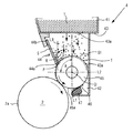
図2は本発明の実施形態に係る現像装置4を含むプロセスカートリッジ1を現像剤担持体(以下、現像ローラという。)45の軸線方向から見た断面図である。図2に示す現像装置4は、現像剤収容室41と現像剤供給室42とが仕切り壁43で区切られて2分割されている。仕切り壁43は、その中央部に現像剤収容室41と現像剤供給室42に連通する開口部43aを設けられている。この開口部43aより現像剤収容室41内の現像剤となるトナーTが現像剤供給室42内に補給(供給)される。
In FIG. 1, a
(First embodiment)
FIG. 2 is a cross-sectional view of the
現像剤供給室42内には、現像ローラ45と、現像ローラ45の表面45aに接触する規制部材44が配置されている。現像ローラ45には感光体2との間に電界を形成させるための現像バイアスが印加されている。本形態において、現像ローラ45は反時計回りの方向に回転し、表面45aに保持したトナーTを規制部材44および感光体2との対向位置へと搬送する。本形態において、規制部材44はブレード部材で構成されていて、そその自由端44aを現像ローラの表面45aに所定の押圧力で当接させたもので、その押圧下を通過したトナーTを薄層化するとともに摩擦帯電によってトナーTに電荷を付与する機能を備えている。この規制部材44には摩擦帯電を補助するために、現像バイアスに対してトナー帯電極性と同方向にオフセットさせた値の規制バイアスが印加される。感光体2は時計回り方向に回転している。従って現像ローラ45の表面45aは感光体2との対向位置において感光体2の進行方向と同方向に移動する。規制部材44で薄層化と帯電されたトナーTは、現像ローラ45の回転によって感光体2との対向位置へ搬送され、現像ローラ45に印加された現像バイアスと感光体2上の静電潜像によって形成される潜像電界に応じて、感光体2の表面2aに移動し現像される。感光体2上に現像されずに現像ローラ45上に残されたトナーが再び現像剤供給室42へ戻る部分には、接触シート46が弾性部材47の弾性力によって現像ローラの表面45aに当接して設けられており、トナーが現像装置4の外部に漏れ出ないように封止している。
In the
本形態では、従来用いていたトナー供給ローラを用いることなく、規制部材44だけを現像ローラの表面45aに当接させているが、単に規制部材44を現像ローラの表面45aに当接させるだけでは、現像ローラ45に対するトナー供給が不十分になり、現像ローラの表面45aに充分なトナー層が形成され難く、画像欠損が発生することが懸念される。このため、規制部材44と現像ローラの表面45aとの接触箇所Pを、現像ローラ45を軸線方向から見て反時計回る方向に移動する際の、符号Aで示す第2象限に配置した。つまり現像ローラ45の回転中心Оで交差する垂直と水平な直線L1、L2を引き、4つの区分される領域のうち、左上の領域である第2象限(A)内において、規制部材44の自由端44aを現像ローラ45の表面45aに接触させて配置した。
In this embodiment, without using the conventionally used toner supply roller, only the regulating
このような配置構成とすることで、図2に破線で示す現像ローラ45の上部が開放状態になり、トナーTの自重により、現像ローラ45にトナーTを十分に供給できるようになる。また、現像ローラ45の反時計り方向への移動に伴いトナーTも同方向に移動しようとするが、規制部材44により規制されるため、規制されたトナーTは、規制部材44と現像ローラの表面45aで形成された空間Sに堆積することになる。しかし現像ローラ45の反時計り方向への移動は継続しているため、空間S内のトナーTが規制部材44によって押し返されて現像ローラ45の回転方向とは反対方向へ戻る流れRが生じるため、規制後のトナーTを充分に規制前のトナーTと混合することができる。
With such an arrangement, the upper part of the developing
このように現像ローラ45に接触する部材が規制部材44の1つになるので、現像ローラ45上のトナーTに対するストレスが低減し、微小化や荷電の低下による印刷画像の白紙部に地汚れの発生や画像ノイズの発生を抑制して良好な画像を得ることができる。また、規制部材44と現像ローラの表面45aとの接触箇所Pを第2象限に配置することで、現像ローラ45に対するトナー供給を十分に行えるので、トナー不足によるトナー層のばらつきが低減し、画像欠損の発生がなくなり、良好な画像を得ることができる。
(第2の実施形態)
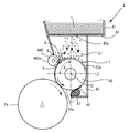
本形態は、図3に示すように、現像剤供給室42内において、仕切り壁43の開口部43aから落下して供給されるトナーTを貯蔵する空間S1を、現像ローラ45の上部のみに形成した。すなわち、第1の実施形態に対して、現像ローラ45の位置を、トナーTの供給方向と交差する側に位置する現像剤供給室42の壁面42aよりで、仕切り壁43の開口部43aの下方に配置し、壁面42aと規制部材44と現像ローラ45の表面45aの上部によって、現像剤供給室42内にトナーTを貯蔵する空間S1を形成するように各部の位置を配置した。
As described above, since the member that contacts the developing
(Second Embodiment)
In this embodiment, as shown in FIG. 3, a space S <b> 1 for storing the toner T that is dropped and supplied from the opening 43 a of the
このような構成とすることで、現像ローラ45の上部近傍のトナーTは、直接に現像ローラ45の上側に供給され、第1の実施形態に比べて、現像ローラ45の側面部、すなわち、壁部42aと現像ローラの表面45aとの間の空間S2へ回りこみや滞留を抑制することができる。このため、現像ローラ45に対するトナー供給量を充分に確保することができ、現像ローラの表面45aに充分なトナー層を形成して画像欠損の発生を防止して良好な画像を得ることができる。
(第3の実施形態)
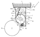
本形態は、図4に示すように、現像剤供給室42内において、現像ローラ45の上部に形成される空間S1にトナーTを攪拌するように回転するパドルなどの攪拌部材48を配置した。このように攪拌部材48を配置すると、空間Sに溜まって空間S1へ戻される規制後のトナーTをより効率的に混合することができる。また、空間Sに溜まって戻される規制後のトナーTを効率的に混合することによって、規制近傍に停滞し、更には、再度規制部となる規制部材44と現像ローラの表面45aとの接触箇所PにトナーTが搬送されることで、よりトナーTの劣化促進されることなく、充填された全体のトナーTが均一に緩和されて劣化が進むことになり、トナーTの耐久性が向上する。
(第4の実施形態)
本形態は、図5に示すように、現像剤供給室42内において、規制部材44の位置を、接触箇所Pを通る鉛直線L3よりも現像ローラ45の回転方向の下流側に配置した。具体的には、規制部材44の自由端44aと反対側の基端44bの位置を、上記実施形態に対して鉛直線L3を基準にして線対称に配置した。なお、必ずしも線対称にする必要は無く、基端44bが鉛直線Lよりも図5中左側に位置する現像ローラ45の回転方向の下流側に配置されていれば良い。
With such a configuration, the toner T in the vicinity of the upper portion of the developing
(Third embodiment)
In this embodiment, as shown in FIG. 4, a stirring
(Fourth embodiment)
In the present embodiment, as shown in FIG. 5, the position of the regulating
このような構成とすると、基端44bが鉛直線L3よりも図5中右方側に位置する場合に比べて、現像ローラの表面45aと規制部材44とで形成される角度θ1が広くなるので、現像ローラ45の上部の空間S1を広くできるとともに、空間S内における現像ローラ45の回転方向に移動するトナーTと逆方向(戻り方向の流れR)に移動するトナーTとの干渉が低減し、空間S内でのトナーTの流れがよりスムーズになり、規制後のトナーTをより効率的に混合することができる。このため、規制近傍に停滞し、更には、再度規制部となる接触箇所PにトナーTが搬送されることで、よりトナーTが劣化促進されることなく、充填された全体のトナーが均一に緩和されて劣化が進むことになり、トナーTの耐久性が向上する。
(第5の実施形態)
本形態は、図6に示すように、規制部材44と現像ローラ45の表面45aの接触箇所Pを、現像ローラ45と感光体2の表面2aとの接触箇所P2に対して、現像ローラ45の回転中心Oを間に挟んで反対側に配置するとともに、現像ローラ45の回転方向に対する第2象限Aに配置した。
With such a configuration, the angle θ1 formed by the
(Fifth embodiment)
In this embodiment, as shown in FIG. 6, the contact point P between the regulating
本発明では、従来から使用していたトナー供給ローラを用いないので、現像ローラ45と感光体2との接触により現像ローラ45が軸線方向において撓むことがある。このため、規制部材44と現像ローラ45の表面45aの接触箇所Pを現像ローラ45と感光体2との接触箇所P1に対して現像ローラ45の回転中心Oを間に挟んで対向する側に配置することで、トナーTに対するストレスを軽減しながら、規制部材44と現像ローラ45との接触圧により現像ローラ45の軸方向への撓みを抑制することができ、トナー層厚ムラをより低減することができる。このため、現像ローラ45上のトナーTに対するストレスが低減し、微小化や荷電の低下による印刷画像の白紙部に地汚れの発生や画像ノイズの発生を抑制しつつも、静電潜像を良好に現像することができるので、より良好な画像を得ることができる。
(第6の実施形態)
本形態は、図7に示すように、規制部材を、円筒形状のローラ部材で構成された規制部材440とした。規制部材440は回転自在であって、現像ローラ45の表面45aにその表面440aが接触するとともに、当該接触箇所Pが第2象限に位置するように配置されている。本形態では、現像ローラ45の表面45aと規制部材440の表面440aで形成される空間Sにおいて戻り方向へのトナーの流れRを発生させるために、規制部材440は、現像ローラ45との対向領域において現像ローラ45の回転方向と逆方向に回転駆動するように構成されている。規制部材440は、トナー供給ローラのように弾性を有するものでは無く、表面440aが平滑に形成された金属製のローラ部材で構成されている。
In the present invention, since the conventionally used toner supply roller is not used, the developing
(Sixth embodiment)
In the present embodiment, as shown in FIG. 7, the regulating member is a regulating
このように規制部材440をローラ部材で構成とすると、規制部材をブレード部材で構成する場合に比べて、空間Sでのトナー流れがスムーズになるとともに、規制部材440が回転することでさらにトナーの流れか良くなり、規制後のトナーTをより効率的に混合することができる。このため、規制近傍に停滞し、更には、再度規制部となる接触箇所PにトナーTが搬送されることで、よりトナーTが劣化促進されることなく、充填された全体のトナーが均一に緩和されて劣化が進むことになり、トナーTの耐久性が向上する。
(第7の実施形態)
本形態は、図8に示すように、現像剤供給室42内において、規制部材44を現像ローラ45の回転方向に複数配置した。本形態では、回転方向の上流側に位置する規制部材441を第1の規制部材とし、下流側に位置する規制部材442を第2の規制部材とした。
In this way, when the regulating
(Seventh embodiment)
In this embodiment, as shown in FIG. 8, a plurality of regulating
第1の規制部材441は、現像ローラ45の表面45a上のトナーの層厚を規制するためのもので、第2の規制部材442は、第1の規制部材441で層厚を規制されたトナーTを摩擦帯電するものである。第1の規制部材441と第2の規制部材442は、共にブレード部材で構成されていて、その自由端441a、442aは、現像ローラ45の表面45aに第2象限で接触するように配置されている。また、第2の規制部材442の自由端442aと現像ローラ45の表面45aとの接触箇所P3での接触圧は、第1の規制部材441の自由端441aと現像ローラ45の表面45aとの接触箇所P2での接触圧よりも低く設定されている。これは、第2の規制部材442の自由端442aと現像ローラ45の表面45aとの接触箇所P3に搬送されるトナーTは、既に第1の規制部材441の自由端441aによって層厚が規制されているので、その総量少なく、第2の規制部材442が接触していれば摩擦帯電するためである。第1の規制部材441の自由端441aと現像ローラ45の表面45aとの接触圧は、トナーTを一定の層厚に規制するため、第2の規制部材442の自由端442aと現像ローラ45の表面45aとの接触圧よりも強めに設定するのが望ましい。
The first restricting
このような構成によると、先の実施形態のように、1つの規制部材44、440を用いる場合に比べて帯電と層厚規制という2つの機能を1つの部材で図ろうとすると、現像ローラ45に対する接触圧を強くしなければならないが、層厚規制用と帯電用の2つの部材を設け、これら規制部材441,442と現像ローラ45の接触箇所P2、P3を第2象限に配置することで、1つの接触箇所に対する接触圧を軽減しつつも、充分にトナーTを摩擦帯電することができるので、感光体2上の静電潜像を良好に現像することができ、良好な画像を形成することにつながる。
According to such a configuration, as in the previous embodiment, compared with the case where one regulating
2 像担持体
42 現像剤供給室
42a 壁面
44 規制部材(ブレード部材)
44a 自由端側
44b 基端側
45 現像剤担持体
45a 現像剤担持体の表面
48 攪拌部材
440 規制部材(ローラ部材)
440a 規制部材の表面
441 第1の規制部材
442 第2の規制部材
A 第2象限
О 回転中心
P 規制部材と現像剤担持体との接触箇所
P1 現像剤担持体と像担持体との接触箇所
L1 垂直な直線(垂直方向に通る直線)
L2 水平な直線
L3 鉛直方向に通る直線
S1 現像剤を貯蔵する空間
T 現像剤
2
44a
440a Surface of
L2 Horizontal straight line L3 Vertical straight line S1 Space for storing developer T Developer
Claims (10)
前記現像剤担持体の表面に接触し、少なくとも同表面上の現像剤の層厚を規制する規制部材を有し、
前記規制部材と前記現像剤担持体との接触箇所が、前記現像剤担持体を軸線方向から見て同現像剤担持体の回転中心で垂直と水平な直線が交わることで区分される象限のうち、前記現像剤担持体の反時計回り方向から見て、第2象限に配置されていることを特徴とする現像装置。 A developer carrier that rotates to supply developer to the image carrier;
A regulating member that contacts the surface of the developer carrying member and regulates the layer thickness of the developer on at least the same surface;
Of the quadrants in which the contact point between the regulating member and the developer carrier is divided by a vertical and horizontal straight line at the rotation center of the developer carrier when the developer carrier is viewed from the axial direction. The developing device is arranged in the second quadrant when viewed from the counterclockwise direction of the developer carrier.
前記現像剤担持体の表面に接触し、少なくとも同表面上の現像剤の層厚を規制する規制部材を有し、
前記規制部材と前記現像剤担持体との接触箇所が、前記現像剤担持体を軸線方向から見て同現像剤担持体の回転中心を垂直方向に通る直線よりも、前記現像剤担持体の回転方向下流側に配置されていることを特徴とする現像装置。 A developer carrier that rotates to supply developer to the image carrier;
A regulating member that contacts the surface of the developer carrying member and regulates the layer thickness of the developer on at least the same surface;
The contact portion between the regulating member and the developer carrying member is more rotated than the straight line passing through the rotation center of the developer carrying member in the vertical direction when the developer carrying member is viewed from the axial direction. A developing device arranged on the downstream side in the direction.
前記現像剤供給内には、前記現像剤担持体の表面と前記規制部材と前記壁面によって、前記現像剤を貯蔵する空間が形成されていることを特徴とする請求項1または2記載の現像装置。 The developer carrier is disposed from a wall surface located on the side intersecting the developer supply direction in the developer supply chamber to which the developer is supplied,
3. The developing device according to claim 1, wherein a space for storing the developer is formed in the developer supply by the surface of the developer carrier, the regulating member, and the wall surface. .
Priority Applications (1)
| Application Number | Priority Date | Filing Date | Title |
|---|---|---|---|
| JP2011252611A JP2013109073A (en) | 2011-11-18 | 2011-11-18 | Developing device, and image forming apparatus |
Applications Claiming Priority (1)
| Application Number | Priority Date | Filing Date | Title |
|---|---|---|---|
| JP2011252611A JP2013109073A (en) | 2011-11-18 | 2011-11-18 | Developing device, and image forming apparatus |
Publications (2)
| Publication Number | Publication Date |
|---|---|
| JP2013109073A true JP2013109073A (en) | 2013-06-06 |
| JP2013109073A5 JP2013109073A5 (en) | 2014-10-16 |
Family
ID=48705911
Family Applications (1)
| Application Number | Title | Priority Date | Filing Date |
|---|---|---|---|
| JP2011252611A Pending JP2013109073A (en) | 2011-11-18 | 2011-11-18 | Developing device, and image forming apparatus |
Country Status (1)
| Country | Link |
|---|---|
| JP (1) | JP2013109073A (en) |
Cited By (2)
| Publication number | Priority date | Publication date | Assignee | Title |
|---|---|---|---|---|
| US9885975B2 (en) | 2014-06-03 | 2018-02-06 | S-Printing Solution Co., Ltd. | Electrophotographic image forming apparatus |
| WO2024042882A1 (en) * | 2022-08-22 | 2024-02-29 | キヤノン株式会社 | Developing device and image forming device |
Citations (8)
| Publication number | Priority date | Publication date | Assignee | Title |
|---|---|---|---|---|
| JPS59100470A (en) * | 1982-12-01 | 1984-06-09 | Fuji Xerox Co Ltd | Developer regulating device of developing device |
| JPS60103373A (en) * | 1983-11-11 | 1985-06-07 | Fuji Xerox Co Ltd | Developing device of electrophotographic copying machine |
| JPH04314069A (en) * | 1991-04-12 | 1992-11-05 | Oki Electric Ind Co Ltd | Developing unit for electrophotographic printer |
| JPH05307319A (en) * | 1992-04-30 | 1993-11-19 | Toshiba Corp | Developing device |
| JPH08179608A (en) * | 1994-12-20 | 1996-07-12 | Sharp Corp | Developing device for image forming device |
| JP2002162824A (en) * | 2000-11-24 | 2002-06-07 | Ricoh Co Ltd | Developing device and image forming device using the same |
| JP2005115082A (en) * | 2003-10-08 | 2005-04-28 | Sharp Corp | Developing device |
| JP2006098854A (en) * | 2004-09-30 | 2006-04-13 | Seiko Epson Corp | Image forming apparatus |
-
2011
- 2011-11-18 JP JP2011252611A patent/JP2013109073A/en active Pending
Patent Citations (8)
| Publication number | Priority date | Publication date | Assignee | Title |
|---|---|---|---|---|
| JPS59100470A (en) * | 1982-12-01 | 1984-06-09 | Fuji Xerox Co Ltd | Developer regulating device of developing device |
| JPS60103373A (en) * | 1983-11-11 | 1985-06-07 | Fuji Xerox Co Ltd | Developing device of electrophotographic copying machine |
| JPH04314069A (en) * | 1991-04-12 | 1992-11-05 | Oki Electric Ind Co Ltd | Developing unit for electrophotographic printer |
| JPH05307319A (en) * | 1992-04-30 | 1993-11-19 | Toshiba Corp | Developing device |
| JPH08179608A (en) * | 1994-12-20 | 1996-07-12 | Sharp Corp | Developing device for image forming device |
| JP2002162824A (en) * | 2000-11-24 | 2002-06-07 | Ricoh Co Ltd | Developing device and image forming device using the same |
| JP2005115082A (en) * | 2003-10-08 | 2005-04-28 | Sharp Corp | Developing device |
| JP2006098854A (en) * | 2004-09-30 | 2006-04-13 | Seiko Epson Corp | Image forming apparatus |
Cited By (2)
| Publication number | Priority date | Publication date | Assignee | Title |
|---|---|---|---|---|
| US9885975B2 (en) | 2014-06-03 | 2018-02-06 | S-Printing Solution Co., Ltd. | Electrophotographic image forming apparatus |
| WO2024042882A1 (en) * | 2022-08-22 | 2024-02-29 | キヤノン株式会社 | Developing device and image forming device |
Similar Documents
| Publication | Publication Date | Title |
|---|---|---|
| US9690233B2 (en) | Developing device, process cartridge, and image forming apparatus incorporating same | |
| JP2013114081A (en) | Image forming apparatus | |
| JP4748242B2 (en) | Developing device and image forming apparatus | |
| JP2013109073A (en) | Developing device, and image forming apparatus | |
| JP2010230754A (en) | Image forming apparatus | |
| JP5210595B2 (en) | Developing device and image forming apparatus including the same | |
| JP2007322570A (en) | Developing roller, developing device, process cartridge and image forming apparatus | |
| JP5510825B2 (en) | Developing device and image forming apparatus having the same | |
| JP5617224B2 (en) | Developing device and image forming apparatus | |
| US10534288B2 (en) | Developing device, process cartridge, and image forming apparatus | |
| JP2006330264A (en) | Developing device | |
| JP2019101349A (en) | Developing device and image forming device equipped with the same | |
| JP5452421B2 (en) | Developing device and image forming apparatus including the same | |
| JP6019923B2 (en) | Powder conveying device, developing device, process cartridge, and image forming apparatus | |
| JP2009198616A (en) | Developing device, process cartridge, and image forming apparatus | |
| JP5464484B2 (en) | Developing device, process cartridge and image forming apparatus having the same | |
| JP2016139111A (en) | Developing device, image forming apparatus, and process cartridge | |
| JP2007241149A (en) | Developing device and image forming apparatus | |
| JP2017203882A (en) | Developing device, process cartridge, and image forming apparatus | |
| JP2017054016A (en) | Conveying device, developing device, and image forming apparatus | |
| JP5948299B2 (en) | Developing device and image forming apparatus | |
| JP5945947B2 (en) | Developing device and image forming apparatus | |
| JP2023064252A (en) | Developing device, process cartridge, and image forming apparatus | |
| JP2023038530A (en) | Developer and image formation device | |
| JP2014021344A (en) | Developer conveying device and developing device including the same, and image forming apparatus |
Legal Events
| Date | Code | Title | Description |
|---|---|---|---|
| A521 | Written amendment |
Free format text: JAPANESE INTERMEDIATE CODE: A523 Effective date: 20140903 |
|
| A621 | Written request for application examination |
Free format text: JAPANESE INTERMEDIATE CODE: A621 Effective date: 20140903 |
|
| A977 | Report on retrieval |
Free format text: JAPANESE INTERMEDIATE CODE: A971007 Effective date: 20150708 |
|
| A131 | Notification of reasons for refusal |
Free format text: JAPANESE INTERMEDIATE CODE: A131 Effective date: 20150714 |
|
| A02 | Decision of refusal |
Free format text: JAPANESE INTERMEDIATE CODE: A02 Effective date: 20151208 |