JP2013102005A - Method of manufacturing semiconductor device, semiconductor device, and manufacturing jig for semiconductor device - Google Patents
Method of manufacturing semiconductor device, semiconductor device, and manufacturing jig for semiconductor device Download PDFInfo
- Publication number
- JP2013102005A JP2013102005A JP2011243981A JP2011243981A JP2013102005A JP 2013102005 A JP2013102005 A JP 2013102005A JP 2011243981 A JP2011243981 A JP 2011243981A JP 2011243981 A JP2011243981 A JP 2011243981A JP 2013102005 A JP2013102005 A JP 2013102005A
- Authority
- JP
- Japan
- Prior art keywords
- semiconductor device
- connector
- long connector
- manufacturing
- lead frame
- Prior art date
- Legal status (The legal status is an assumption and is not a legal conclusion. Google has not performed a legal analysis and makes no representation as to the accuracy of the status listed.)
- Granted
Links
Images


Classifications
-
- H—ELECTRICITY
- H01—ELECTRIC ELEMENTS
- H01L—SEMICONDUCTOR DEVICES NOT COVERED BY CLASS H10
- H01L24/00—Arrangements for connecting or disconnecting semiconductor or solid-state bodies; Methods or apparatus related thereto
- H01L24/01—Means for bonding being attached to, or being formed on, the surface to be connected, e.g. chip-to-package, die-attach, "first-level" interconnects; Manufacturing methods related thereto
- H01L24/34—Strap connectors, e.g. copper straps for grounding power devices; Manufacturing methods related thereto
- H01L24/39—Structure, shape, material or disposition of the strap connectors after the connecting process
- H01L24/40—Structure, shape, material or disposition of the strap connectors after the connecting process of an individual strap connector
-
- H—ELECTRICITY
- H01—ELECTRIC ELEMENTS
- H01L—SEMICONDUCTOR DEVICES NOT COVERED BY CLASS H10
- H01L24/00—Arrangements for connecting or disconnecting semiconductor or solid-state bodies; Methods or apparatus related thereto
- H01L24/01—Means for bonding being attached to, or being formed on, the surface to be connected, e.g. chip-to-package, die-attach, "first-level" interconnects; Manufacturing methods related thereto
- H01L24/34—Strap connectors, e.g. copper straps for grounding power devices; Manufacturing methods related thereto
- H01L24/36—Structure, shape, material or disposition of the strap connectors prior to the connecting process
- H01L24/37—Structure, shape, material or disposition of the strap connectors prior to the connecting process of an individual strap connector
-
- H—ELECTRICITY
- H01—ELECTRIC ELEMENTS
- H01L—SEMICONDUCTOR DEVICES NOT COVERED BY CLASS H10
- H01L24/00—Arrangements for connecting or disconnecting semiconductor or solid-state bodies; Methods or apparatus related thereto
- H01L24/80—Methods for connecting semiconductor or other solid state bodies using means for bonding being attached to, or being formed on, the surface to be connected
- H01L24/84—Methods for connecting semiconductor or other solid state bodies using means for bonding being attached to, or being formed on, the surface to be connected using a strap connector
-
- H—ELECTRICITY
- H01—ELECTRIC ELEMENTS
- H01L—SEMICONDUCTOR DEVICES NOT COVERED BY CLASS H10
- H01L2224/00—Indexing scheme for arrangements for connecting or disconnecting semiconductor or solid-state bodies and methods related thereto as covered by H01L24/00
- H01L2224/01—Means for bonding being attached to, or being formed on, the surface to be connected, e.g. chip-to-package, die-attach, "first-level" interconnects; Manufacturing methods related thereto
- H01L2224/34—Strap connectors, e.g. copper straps for grounding power devices; Manufacturing methods related thereto
- H01L2224/39—Structure, shape, material or disposition of the strap connectors after the connecting process
- H01L2224/40—Structure, shape, material or disposition of the strap connectors after the connecting process of an individual strap connector
- H01L2224/4005—Shape
- H01L2224/4009—Loop shape
- H01L2224/40095—Kinked
-
- H—ELECTRICITY
- H01—ELECTRIC ELEMENTS
- H01L—SEMICONDUCTOR DEVICES NOT COVERED BY CLASS H10
- H01L2224/00—Indexing scheme for arrangements for connecting or disconnecting semiconductor or solid-state bodies and methods related thereto as covered by H01L24/00
- H01L2224/01—Means for bonding being attached to, or being formed on, the surface to be connected, e.g. chip-to-package, die-attach, "first-level" interconnects; Manufacturing methods related thereto
- H01L2224/34—Strap connectors, e.g. copper straps for grounding power devices; Manufacturing methods related thereto
- H01L2224/39—Structure, shape, material or disposition of the strap connectors after the connecting process
- H01L2224/40—Structure, shape, material or disposition of the strap connectors after the connecting process of an individual strap connector
- H01L2224/401—Disposition
- H01L2224/40135—Connecting between different semiconductor or solid-state bodies, i.e. chip-to-chip
- H01L2224/40137—Connecting between different semiconductor or solid-state bodies, i.e. chip-to-chip the bodies being arranged next to each other, e.g. on a common substrate
- H01L2224/40139—Connecting between different semiconductor or solid-state bodies, i.e. chip-to-chip the bodies being arranged next to each other, e.g. on a common substrate with an intermediate bond, e.g. continuous strap daisy chain
-
- H—ELECTRICITY
- H01—ELECTRIC ELEMENTS
- H01L—SEMICONDUCTOR DEVICES NOT COVERED BY CLASS H10
- H01L2224/00—Indexing scheme for arrangements for connecting or disconnecting semiconductor or solid-state bodies and methods related thereto as covered by H01L24/00
- H01L2224/80—Methods for connecting semiconductor or other solid state bodies using means for bonding being attached to, or being formed on, the surface to be connected
- H01L2224/84—Methods for connecting semiconductor or other solid state bodies using means for bonding being attached to, or being formed on, the surface to be connected using a strap connector
- H01L2224/848—Bonding techniques
- H01L2224/84801—Soldering or alloying
-
- H—ELECTRICITY
- H01—ELECTRIC ELEMENTS
- H01L—SEMICONDUCTOR DEVICES NOT COVERED BY CLASS H10
- H01L2924/00—Indexing scheme for arrangements or methods for connecting or disconnecting semiconductor or solid-state bodies as covered by H01L24/00
- H01L2924/0001—Technical content checked by a classifier
- H01L2924/00014—Technical content checked by a classifier the subject-matter covered by the group, the symbol of which is combined with the symbol of this group, being disclosed without further technical details
Abstract
Description
本発明は、複数の半導体チップを1つの長尺接続子によって接続している内部接続構造を有する半導体装置の製造方法、当該半導体装置の製造方法によって製造された半導体装置及び前記半導体装置の製造方法に用いるための半導体装置の製造用治具に関する。 The present invention relates to a method of manufacturing a semiconductor device having an internal connection structure in which a plurality of semiconductor chips are connected by one long connector, a semiconductor device manufactured by the method of manufacturing the semiconductor device, and a method of manufacturing the semiconductor device The present invention relates to a semiconductor device manufacturing jig for use in manufacturing.
複数の半導体チップを1つの接続子によって接続することは従来から行われている(例えば、特許文献1参照。)。 Conventionally, a plurality of semiconductor chips are connected by a single connector (see, for example, Patent Document 1).
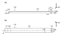
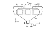
図9は、特許文献1に開示されている半導体装置の内部接続構造の一例を説明するために示す図である。特許文献1に開示されている半導体装置の内部接続構造は、図9に示すように、ダイパッド811、812,813に搭載されている半導体チップ821,822,823を、1つの接続子830によって共通接続するような内部接続構造となっており、このような内部接続構造において、半導体チップ821,822,823の配列方向と、接続子830の延出方向とが交差するような内部接続構造となっている。この場合、半導体チップ821,822,823の配列方向はx軸に沿った方向であり、接続子830の延出方向はy軸に沿った方向であるため、両者は直交関係にある。
FIG. 9 is a diagram shown for explaining an example of the internal connection structure of the semiconductor device disclosed in
複数の半導体チップを1つの接続子で接続する場合、図9に示すような内部接続構造とすることにより、複数の半導体チップを安定した状態で接続することができる。なお、図9においては、接続子830は、リードフレームのコネクタ部840に接続子830の基端部850のみが支持された状態となっている。このように、リードフレームのコネクタ部に基端部のみが支持された状態で当該リードフレームに取り付けられている接続子を、「片側支持の接続子」と呼ぶことにする。
When a plurality of semiconductor chips are connected with one connector, the plurality of semiconductor chips can be stably connected by adopting an internal connection structure as shown in FIG. In FIG. 9, the
特許文献1に開示されている半導体装置の内部接続構造においては、複数の半導体チップ821,822,823の配列方向と接続子830の延出方向とが交差するように接続子830を配置して、当該接続子830によって複数の半導体チップ821,822,823を共通接続しているが、半導体装置の種類によっては、片側支持の接続子を複数の半導体の配列方向に沿うように配置して、当該接続子によって複数の半導体チップを共通接続するような内部接続構造を採用するものもある。この場合の接続子は、複数の半導体の配列方向に沿うように配置されるため、長尺の接続子(長尺接続子という。)が用いられる。
In the internal connection structure of the semiconductor device disclosed in
図10は、長尺接続子によって複数の半導体チップを共通接続するような半導体装置900の内部接続構造について説明するために示す図である。なお、図10は半導体装置900の内部接続構造を側断面図として示している。なお、半導体装置900において用いられている長尺接続子910は、全体的には、細長い薄板状をなしており、図10に示すように、基端部911と、立ち上がり部912と、接続板部913とを有している。また、当該長尺接続子910は、基端部911がリードフレーム920のコネクタ部925に固定されている「片側支持の長尺接続子」である。
FIG. 10 is a diagram for explaining an internal connection structure of a
半導体装置900の内部接続構造は、このような長尺接続子910によって、リードフレーム920のダイパッド921、922,923にx軸に沿って配列された複数(3個とする。)の半導体チップ931,932,933を共通接続している。
また、長尺接続子910の接続板部913と各半導体チップ931,932,933とは半田付けによって接続され、長尺接続子810の接続板部913の下面と各半導体チップ931,932,933の上面との間には半田層950が形成されている。なお、以下では、「長尺接続子910の接続板部913と各半導体チップ931,932,933とを半田付する」というような表記を行う場合、「接続板部」を省略して、「長尺接続子と各半導体チップとを半田付けする」というように表記する場合もある。
The internal connection structure of the
The
なお、基端部911を延長した基端部延長線(図10における破線で示す。)と接続板部913とは平行となっている。また、長尺接続子910の接続板部913の長さL0は、図10に示すように、3個の半導体チップ931,932,933を共通接続したときに、長尺接続子910の先端部910aが、当該長尺接続子910の先端部910a側に位置する半導体チップ933を覆うことができる程度の長さとしている。
In addition, the base end part extension line (it shows with the broken line in FIG. 10) which extended the
このような片側支持の長尺接続子910を用いて、図10に示すように、3個の半導体チップ931,932,933を共通接続する場合、長尺接続子910の先端部910a側に位置する半導体チップほど、長尺接続子910の接続板部913の撓みによる当該接続板部913の重みが半導体チップに加わる。特に、長尺接続子910の最も先端側に位置する半導体チップ933においては、接続板部913の撓みがより大きくなり、当該接続板部913の重みが半導体チップ933に加わる。
When the three
このため、半導体チップ933と長尺接続子910の接続板部913との間隔t2は、適正間隔(半導体チップ931と長尺接続子910の接続板部913との間隔t1とする。)に比べて小さくなり、半導体チップ933に形成される半田層950が押し潰されて、半田が半導体チップ933の外周に回り込むことがある。その結果、図示しない他の部品や配線との絶縁距離が不足して短絡などが生じるおそれがある。また、半田層950の厚みが薄くなると、温度サイクルなどによる耐候性が劣化するといった課題が生じる。
For this reason, the interval t2 between the
本発明は、片側支持の長尺接続子を用いて直線上に配列された複数の半導体チップを半田付けにより共通接続する場合において、長尺接続子の接続板部の撓みを防止して当該長尺接続子の接続板部と各半導体チップとの間隔を適正間隔に保持することにより、長尺接続子と各半導体チップとの間の半田付けの状態を適切な状態とすることができる半導体装置の製造方法を提供することを目的とする。また、このような半導体装置の製造方法によって半導体装置を製造することにより、長尺接続子と各半導体チップとの間の半田付けの状態が適切な状態に保持されている半導体装置を提供することを目的とする。また、このような半導体装置の製造方法に用いるための半導体装置の製造用治具を提供することを目的とする。 In the case where a plurality of semiconductor chips arranged in a straight line are commonly connected by soldering using a single-side supported long connector, the present invention prevents the connection plate portion of the long connector from being bent. A semiconductor device capable of bringing the soldering state between the long connector and each semiconductor chip into an appropriate state by maintaining the distance between the connecting plate portion of the long connector and each semiconductor chip at an appropriate interval. It aims at providing the manufacturing method of. Further, by providing a semiconductor device by such a method for manufacturing a semiconductor device, a semiconductor device in which the state of soldering between the long connector and each semiconductor chip is maintained in an appropriate state is provided. With the goal. It is another object of the present invention to provide a semiconductor device manufacturing jig for use in such a method of manufacturing a semiconductor device.
[1]本発明の半導体装置の製造方法は、複数の半導体チップが直線上に沿った配列となるように前記複数の半導体チップを個々の半導体チップごとに搭載する複数のダイパッドを有するとともに、前記ダイパッドとは離隔した位置でかつ前記複数の半導体チップの配列方向に沿った位置に設けられるコネクタ部を有するリードフレームと、前記コネクタ部に基端部が固定され、前記基端部とは反対側の先端部と前記基端部との間の接続板部で前記複数の半導体素子を共通接続する長尺接続子とを備え、前記複数の半導体チップの各上面と前記長尺接続子の前記接続板部の下面とが半田付けによって接続されている内部接続構造を有する半導体装置の製造方法であって、前記長尺接続子として、前記接続板部を前記複数の半導体チップのうち当該長尺接続子の先端部の側に位置する半導体チップよりもさらに先方にまで延長することによって形成された延長部を有するとともに、前記延長部の下面に下方向に突出する突起部を有する長尺接続子を準備する工程と、前記リードフレームを当該リードフレームの下面側から支持するようにして載置するリードフレーム載置面を有するとともに、当該リードフレーム載置面に、前記長尺接続子の突起部を当接させるための突起当接部を有する台座を準備する工程と、前記長尺接続子の突起部を前記台座の突起当接部に当接させるように前記リードフレームを前記台座に載置した状態で前記複数の半導体チップの各上面と前記長尺接続子の前記接続板部の下面とを半田付けする工程とを有し、前記長尺接続子の突起部の高さ及び前記台座の突起当接部は、前記長尺接続子の突起部を前記台座の突起当接部に当接させるように前記リードフレームを前記台座に載置した状態としたときに、前記各半導体チップの各上面を結ぶ平面と前記長尺接続子の前記接続板部の下面とが平行となるように前記長尺接続子の突起部の突出長さ及び前記台座の突起当接部の高さが設定されていることを特徴とする。 [1] A method of manufacturing a semiconductor device according to the present invention includes a plurality of die pads for mounting the plurality of semiconductor chips for each semiconductor chip so that the plurality of semiconductor chips are arranged along a straight line. A lead frame having a connector portion provided at a position separated from the die pad and along the arrangement direction of the plurality of semiconductor chips, and a base end portion fixed to the connector portion, opposite to the base end portion A long connector that commonly connects the plurality of semiconductor elements at a connecting plate portion between the distal end portion and the base end portion, and the connection between each upper surface of the plurality of semiconductor chips and the long connector. A method of manufacturing a semiconductor device having an internal connection structure in which a lower surface of a plate portion is connected by soldering, wherein the connection plate portion is used as the long connector among the plurality of semiconductor chips. A length having an extension formed by extending further forward than the semiconductor chip located on the tip side of the long connector, and a protrusion protruding downward on the lower surface of the extension And a lead frame mounting surface for mounting the lead frame so as to support the lead frame from the lower surface side of the lead frame, and the long connector on the lead frame mounting surface. A step of preparing a pedestal having a protrusion abutting part for abutting the protruding part of the long connector, and the lead frame to the pedestal so as to abut the protruding part of the elongated connector against the protrusion abutting part of the pedestal Soldering the upper surface of each of the plurality of semiconductor chips and the lower surface of the connection plate portion of the long connector in a state of being placed on the height of the protrusion of the long connector, and Of the pedestal When the lead frame is placed on the pedestal so that the protruding portion of the long connector contacts the protruding contact portion of the pedestal, The protruding length of the protrusion of the long connector and the height of the protrusion contact portion of the pedestal are set so that the plane connecting the upper surface and the lower surface of the connecting plate portion of the long connector are parallel to each other. It is characterized by.
[2]本発明の半導体装置の製造方法においては、前記長尺接続子の突起部は、当該長尺接続子を下面側から見たときの形状が前記接続板部の幅方向に大きく、前記接続板部の長手方向に小さい細長形状をなしていることが好ましい。 [2] In the method for manufacturing a semiconductor device of the present invention, the protrusion of the long connector has a large shape in the width direction of the connection plate when the long connector is viewed from the lower surface side. It is preferable that the connecting plate portion has a small elongated shape in the longitudinal direction.
[3]本発明の半導体装置の製造方法においては、前記突起部における前記接続板部の幅方向の寸法は、前記接続板部の幅方向と同等又は当該接続板部の幅方向よりもわずかに短い長さとすることが好ましい。 [3] In the method for manufacturing a semiconductor device according to the present invention, the dimension in the width direction of the connection plate portion in the protrusion is equal to or slightly smaller than the width direction of the connection plate portion. A short length is preferred.
[4]本発明の半導体装置の製造方法においては、前記台座の前記突起当接部は、上方向に突出する凸部であることが好ましい。 [4] In the method for manufacturing a semiconductor device of the present invention, it is preferable that the protrusion contact portion of the pedestal is a protrusion protruding upward.
[5]本発明の半導体装置の製造方法においては、前記凸部の高さは、前記リードフレームの板厚以下とすることが好ましい。 [5] In the method for manufacturing a semiconductor device of the present invention, it is preferable that the height of the convex portion is equal to or less than the plate thickness of the lead frame.
[6]本発明の半導体装置は、複数の半導体チップが直線上に沿った配列となるように前記複数の半導体チップを個々の半導体チップごとに搭載する複数のダイパッドを有するとともに、前記ダイパッドとは離隔した位置でかつ前記複数の半導体チップの配列方向に沿った位置に設けられるコネクタ部を有するリードフレームと、前記コネクタ部に基端部が固定され、前記基端部とは反対側の先端部と前記基端部との間の接続板部で前記複数の半導体素子を共通接続する長尺接続子とを備え、前記複数の半導体チップの各上面と前記長尺接続子の前記接続板部の下面とが半田付けによって接続されている内部接続構造を有する半導体装置であって、当該半導体装置は、[1]〜[5]のいずれかの半導体装置の製造方法によって製造されたものであることを特徴とする。 [6] The semiconductor device of the present invention has a plurality of die pads for mounting the plurality of semiconductor chips for each individual semiconductor chip so that the plurality of semiconductor chips are arranged along a straight line. A lead frame having a connector portion provided at a position separated from each other and along the arrangement direction of the plurality of semiconductor chips, and a proximal end portion fixed to the connector portion, and a distal end portion opposite to the proximal end portion And a long connector for commonly connecting the plurality of semiconductor elements at a connection plate portion between the base end portion and the upper surface of the plurality of semiconductor chips and the connection plate portion of the long connector. A semiconductor device having an internal connection structure in which a lower surface is connected by soldering, and the semiconductor device is manufactured by the method for manufacturing a semiconductor device according to any one of [1] to [5]. And characterized in that.
[7]本発明の半導体装置の製造用治具は、[1]〜[5]のいずれかに記載の半導体装置の製造方法によって半導体装置を製造する際に用いるための半導体装置の製造用治具であって、前記リードフレームを当該リードフレームの下面側から支持するようにして載置するリードフレーム載置面を有するとともに、当該リードフレーム載置面に、前記長尺接続子の突起部を当接させるための突起当接部を有する台座を備えていることを特徴とする。 [7] A jig for manufacturing a semiconductor device according to the present invention is a jig for manufacturing a semiconductor device for use in manufacturing a semiconductor device by the method for manufacturing a semiconductor device according to any one of [1] to [5]. A lead frame mounting surface for mounting the lead frame so as to support the lead frame from the lower surface side of the lead frame, and a protrusion of the long connector on the lead frame mounting surface. A pedestal having a projecting contact portion for contacting is provided.
本発明の半導体装置の製造方法は、接続板部を延長することによって形成された延長部の下面側に下方向に突出する突起部を有する長尺接続子と、当該突起部を当接させるための突起当接部を有する台座とを用い、長尺接続子の突起部を台座の突起当接部に当接させるようにリードフレームを台座に載置した状態で、複数の半導体チップの各上面と長尺接続子の接続板部の下面と半田付けするようにしている。なお、長尺接続子の突起部の突出長さ及び台座の突起当接部の高さは、長尺接続子の突起部を台座の突起当接部に当接させるようにリードフレームを台座に載置した状態としたときに、各半導体チップの各上面を結ぶ平面と接続板部の下面とが平行となるように設定されている。 In the method for manufacturing a semiconductor device of the present invention, a long connector having a protrusion protruding downward on the lower surface side of an extension formed by extending a connection plate is brought into contact with the protrusion. Each of the upper surfaces of the plurality of semiconductor chips in a state where the lead frame is placed on the pedestal so that the protruding portion of the long connector contacts the protruding contact portion of the pedestal. And soldering to the lower surface of the connecting plate portion of the long connector. Note that the protrusion length of the protrusion of the long connector and the height of the protrusion contact portion of the pedestal are set so that the protrusion of the long connector contacts the protrusion contact portion of the pedestal. When placed, the plane connecting each upper surface of each semiconductor chip and the lower surface of the connecting plate portion are set to be parallel.
このため、本発明の半導体装置の製造方法によれば、片側支持の長尺接続子を用いて直線上に配列された複数の半導体チップを半田付けにより共通接続するような場合において、接続板部の撓みを防止して当該接続板部と各半導体チップとの間隔を適正間隔に保持することにより、長尺接続子と各半導体チップとの間の半田付けの状態を適切な状態とすることができる。 Therefore, according to the method for manufacturing a semiconductor device of the present invention, in the case where a plurality of semiconductor chips arranged in a straight line are commonly connected by soldering using a single-side supported long connector, the connection plate portion The soldering state between the long connector and each semiconductor chip can be made to be in an appropriate state by keeping the distance between the connection plate portion and each semiconductor chip at an appropriate interval by preventing the bending of the semiconductor chip. it can.
また、本発明の半導体装置は、前記半導体装置の製造方法によって製造されたものであるため、本発明の半導体装置によれば、前記本発明の半導体装置の製造方法によって得られる効果と同様の効果が得られる。また、本発明の半導体装置は、長尺接続子に突起部が存在しているため、半田付け工程の後に行われる樹脂封止工程によって樹脂封止された場合に、モールドロックの効果が得られ、耐久性に優れた半導体装置とすることができる。また、本発明の半導体装置は、長尺接続子に突起部が存在していることにより、長尺接続子の表面積が大きくなるため、放熱性向上の効果も得られる。 Further, since the semiconductor device of the present invention is manufactured by the method for manufacturing a semiconductor device, according to the semiconductor device of the present invention, the same effect as that obtained by the method for manufacturing a semiconductor device of the present invention is used. Is obtained. Further, since the semiconductor device of the present invention has a protrusion on the long connector, the effect of mold lock can be obtained when resin sealing is performed by a resin sealing process performed after the soldering process. Thus, a semiconductor device having excellent durability can be obtained. In addition, since the semiconductor device of the present invention has a protrusion on the long connector, the surface area of the long connector is increased, so that an effect of improving heat dissipation can also be obtained.
また、本発明の半導体装置の製造用治具を上記半導体装置の製造方法において用いることにより、半導体装置を製造する際の製造工程を容易かつ適切に行うことができる。 In addition, by using the semiconductor device manufacturing jig of the present invention in the semiconductor device manufacturing method, the manufacturing process for manufacturing the semiconductor device can be performed easily and appropriately.
以下、本発明の実施形態について説明する。 Hereinafter, embodiments of the present invention will be described.
[実施形態1]
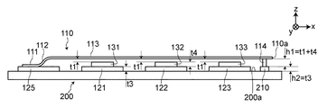
図1は、実施形態1に係る半導体装置10の内部接続構造を説明するために示す図である。なお、図1は半導体装置10の側断面図であり、樹脂封止工程を行う前の状態を示している。半導体装置10の内部接続構造は、基本的には、図10に示した半導体装置900と同様の内部接続構造となっているが、長尺接続子110の構成が図10に示した半導体装置900において用いられている長尺接続子910と少し異なっている。
[Embodiment 1]
FIG. 1 is a diagram for explaining the internal connection structure of the semiconductor device 10 according to the first embodiment. FIG. 1 is a side sectional view of the semiconductor device 10 and shows a state before the resin sealing step. The internal connection structure of the semiconductor device 10 is basically the same internal connection structure as the
実施形態1に係る半導体装置10において用いられる長尺接続子110の全体的な外観形状は、図10に示した長尺接続子810と同様に、細長い薄板状をなし、基端部111と、立ち上がり部112と、接続板部113とを有しており、基端部111がリードフレーム120のコネクタ部125に固定されている片側支持の長尺接続子である。なお、長尺接続子110においても、基端部111を延長した基端部延長線(図1における破線で示す。)と接続板部113とは平行となっている。
The overall appearance of the
このような長尺接続子110が図10に示した長尺接続子910と異なるのは、接続板部113を長尺接続子110の先端部110aの側に位置する半導体チップ133よりもさらに先方にまで延長することによって形成された延長部115を有することと、当該延長部115の下面に下方向に突出する突起部114を有することである。なお、延長部115のx軸方向長さL1(図1参照。)は、例えば、1つの半導体チップのx軸に沿った寸法と同程度でよい。また、突起部114の突出長さh1(突起部114の高さh1ともいう。)については後述する。
Such a
実施形態1に係る半導体装置10の内部接続構造は、このような長尺接続子110を用いて、リードフレーム120のダイパッド121、122,123に直線上に配列(x軸上に沿うように配列)された複数(3個とする。)の半導体チップ131,132,133を共通接続するような内部接続構造となっている。なお、半導体チップ131,132,133のそれぞれの厚みはそれぞれ同じ厚み(t4とする。)であるとする。
The internal connection structure of the semiconductor device 10 according to the first embodiment is arranged linearly on the
また、長尺接続子110の接続板部113と各半導体チップ131,132,133とは半田付けによって接続され、長尺接続子110の接続板部113の下面と各半導体チップ131,132,133の上面との間には半田層150が形成されている
The
図2は、実施形態1に係る半導体装置10において用いる長尺接続子110を説明するために示す図である。図2(a)は長尺接続子110の側面図であり、図2(b)は長尺接続子110を下方向(裏面)から見た平面図である。長尺接続子110は、上記したように、接続板部113を延長することにより形成された延長部115を有するとともに、当該延長部115の下面に下方向に突出する突起部114を有する。
FIG. 2 is a view for explaining the
突起部114を下面側から見たときの平面形状は、図2(b)に示すように、長尺接続子110の接続板部113の幅方向(y軸に沿った方向)に長く、当該長尺接続子110の接続板部113の長手方向(x軸に沿った方向)に短い細長形状(例えば細長い長円形)としている。なお、突起部114のy軸方向の寸法L2は、長尺接続子110の接続板部113の幅方向の寸法L3に可能な限り近い寸法が好ましい。なお、このような突起部114はプレス加工によって形成することができる。
The planar shape when the
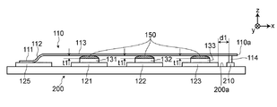
図3は、実施形態1に係る半導体装置10を製造する際に用いる台座200を説明するために示す図である。図3(a)は台座200の側断面図を示す図であり、図3(b)は台座200の一部を示す平面図であり、図3(c)は半導体チップ131,132,133がダイパッド121,122,123に搭載されているリードフレーム120を台座200に載置した状態を示す図である。なお、台座200は例えばカーボン製でなる。
FIG. 3 is a view for explaining the
台座200は、上面がリードフレーム載置面200aとなっており、当該リードフレーム載置面200aの所定位置(長尺接続子110の突起部114に対向する位置)に、長尺接続子110の突起部114を当接させるための突起当接部210を有している。この突起当接部210は、実施形態1においては、上方に突出した台状の凸部としている。このため、実施形態1においては、突起当接部210を凸部210ともいう。
The upper surface of the
なお、凸部210の台座200のリードフレーム載置面200aからの高さh2は、リードフレーム120の板厚t3以下とすることが好ましい。これは、台座200がカーボン製でなる場合、カーボンが脆い素材であるために、凸部210を必要以上に高くすると、凸部210が破損しやすくなるためである。このような凸部210は台座200を切削加工することによって形成することができる実施形態1においては、凸部210の高さh2は、リードフレーム120の板厚t3としている。
Note that the height h2 of the
このように構成された台座200は、半導体装置10を製造する際の半導体装置の製造用治具の1つとして用いられる。なお、半導体装置の製造用治具全体の図示及び説明は省略する。そして、このような台座200は半導体製造工程のうち、長尺接続子110と半導体チップ131,132,133とを半田付けする半田付け工程において用いられるものであり、当該半田付け工程の終了後おいては取り外される。
The
図4は、長尺接続子110と、半導体チップ131,132,133がダイパッド121,122,123に搭載されているリードフレーム120と、台座200との配置について説明するために示す図である。なお、図4は半田付け工程を行う前の状態を示しているが、長尺接続子110の基端部111はリードフレーム120のコネクタ部125に固定されている状態が示されている。
FIG. 4 is a view for explaining the arrangement of the
図4に示すような状態で、長尺接続子110の突起部114を台座200の凸部210に当接させるようにリードフレーム120を台座200に載置すると、長尺接続子110の接続板部113は撓むことがないため、長尺接続子110の接続板部113の下面と台座200のリードフレーム載置面200aとは平行となる。すなわち、半導体チップ131,132,133の各上面を結ぶ平面と長尺接続子110の接続板部113の下面とが平行となる。これにより、ダイパッド121,122,123に搭載されている各半導体チップ131,132,133の上面と長尺接続子110の接続板部113の下面との間隔は、どの半導体チップにおいても同じ間隔(この場合、適正間隔t1)となる。
In the state shown in FIG. 4, when the
このようにするには、長尺接続子110に設けられている突起部114の高さh1と台座200の凸部210の高さh2とを足した合計の高さ(h1+h2)が、h1+h2=t1+t3+t4となるように設定すればよい。すなわち、長尺接続子110に設けられている突起部114の高さh1と台座200の凸部210の高さh2とを足した合計の高さ(h1+h2)が、適正間隔t1とリードフレーム120の板厚t3と半導体チップ131,132,133のそれぞれの厚みt4とを足した値(t1+t3+t4)となるように設定すればよい。なお、実施形態1においては、台座200の凸部210の高さh2をリードフレーム120の板厚t3としているため、長尺接続子110の突出長さh1は、適正間隔t1に半導体チップの厚みt4を足した値(t1+t4)に設定すればよい。
To do this, the total height (h1 + h2) obtained by adding the height h1 of the
長尺接続子110の突起部114の高さh1と台座200の凸部210の高さh2をこのように設定することにより、長尺接続子110の接続板部113が下方向に撓むことがなくなり、半導体チップ131,132,133の上面と長尺接続子110の接続板部113の下面との間隔をどの半導体チップおいても適正間隔t1とすることができる。
By setting the height h1 of the
図5は、半田付け工程により長尺接続子110と半導体チップ131,132,133とを半田付けした状態を示す図である。図5に示すように、半導体チップ131,132,133がダイパッド121,122,123に搭載されたリードフレーム120を台座200に載置した状態とし、かつ、長尺接続子110の突起部114を台座200の凸部210に当接させた状態(図4参照。)で、長尺接続子110の接続板部113と半導体チップ131,132,133とを半田付けすると、長尺接続子110の接続板部113と半導体チップ131,132,133との間に形成される半田層150の厚みは、どの半導体チップにおいても適正な厚み(適正間隔t1に対応する厚み)とすることができる。
FIG. 5 is a diagram illustrating a state in which the
これは、図4において説明したように、長尺接続子110の突起部114と台座200の凸部210とが当接した状態となっていることにより、長尺接続子110の接続板部113が下方向に撓むことがなくなり、半導体チップ131,132,133の上面と長尺接続子110の接続板部113の下面との間隔をどの半導体チップおいても適正間隔t1とすることができるからである。これにより、半田層150の潰れを確実に防止することができ、それによって、半田層150の厚みを適正な厚みとすることができる。
As described with reference to FIG. 4, the
ところで、前述したように、長尺接続子110の突起部114の平面形状は、長尺接続子110の接続板部113の幅方向(y軸に沿った方向)に長く、当該長尺接続子110の接続板部113の長手方向(x軸に沿った方向)に短い細長形状としている。長尺接続子110の突起部114の平面形状をこのような形状としたのは、突起部114に近接する部品(例えば、半導体チップ133及びダイパッド123)との最短距離d1(図5参照。)を可能な限り大きくとることができるようにするとともに、当該突起部114を台座200の凸部210に当接させた状態としたときに、長尺接続子110の幅方向の安定感を持たせることができるようにするためである。
Incidentally, as described above, the planar shape of the
すなわち、長尺接続子110の突起部114の平面形状がx軸に沿った方向において短い細長形状であることにより、近接する部品と間の最短距離d1をより大きく確保することができる。仮に、長尺接続子110の突起部114の平面形状がx軸に沿った方向においても長い形状であると、突起部114と近接する部品との距離が近くなり過ぎる場合もあり、絶縁性などに課題が生じるおそれもある。これに対処するために、実施形態1においては、長尺接続子110の突起部114の平面形状がx軸に沿った方向に短い細長形状としている。
That is, since the planar shape of the
また、長尺接続子110の突起部114の平面形状がy軸に沿った方向において長い細長形状であることにより、当該突起部114を台座200の凸部210に当接させた状態としたときに、長尺接続子110のx軸に沿った中心軸m(図2(b)参照。)を中心とした回転力が当該長尺接続子110に働きにくくなり、それによって長尺接続子110の幅方向の水平度を保持しやすくなる。
In addition, when the planar shape of the
なお、図5に示すような半田付け工程がなされたあとは、台座200は取り外す。一方、長尺接続子110の突起部114は、図5に示すような半田付け工程がなされたあとにおいても切除する必要は特にない。むしろ、突起部114が存在していることにより、後に行われる樹脂樹脂封止工程によって樹脂封止された場合に、モールドロックの効果が得られる。また、突起部114が存在していることにより、長尺接続子110の表面積が大きくなるため、放熱性向上の効果も得られる。
Note that the
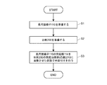
図6は、実施形態1に係る半導体装置10を製造するための製造工程の説明するフローチャートである。なお、図6に示すフローチャートは実施形態1に係る半導体装置10を製造する工程のうち、長尺接続子110と半導体チップ131,132,133とを半田付けする半田付け工程までを示すものある。
FIG. 6 is a flowchart illustrating a manufacturing process for manufacturing the semiconductor device 10 according to the first embodiment. Note that the flowchart shown in FIG. 6 shows the soldering process for soldering the
実施形態1に係る半導体装置10を製造する際の製造工程は、図6に示すように、長尺接続子として図2に示したような長尺接続子110を準備する工程(ステップS1)と、図3に示したような台座200を準備する工程(ステップS2)と、長尺接続子110の突起部114を台座200の突起当接部(凸部)210に当接させるようにリードフレーム120を台座200に載置した状態で半導体チップ131,132,133の各上面と長尺接続子110の接続板部113の下面とを図5に示すように半田付けする工程(ステップS3)とを有する。
As shown in FIG. 6, the manufacturing process for manufacturing the semiconductor device 10 according to the first embodiment is a process of preparing the
このような工程を実施することにより、長尺接続子110の接続板部113が下方向に撓むことがなくなり、半導体チップ131,132,133の上面と長尺接続子110の接続板部113の下面との間隔をどの半導体チップおいても適正間隔t1とすることができる。これにより、半田層150の潰れを確実に防止することができ、それによって、半田層150の厚みを適正な厚みとすることができる。
By performing such a process, the
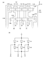
図7は、図6に示す半導体装置の製造工程を適用可能な半導体装置の一例を示す図である。図7(a)は半導体装置としての3相ブリッジダイオードの構成を模式的に示す図であり、図7(b)は図7(a)に示す3相ブリッジダイオードに対応する回路構成を示す図である。 FIG. 7 is a diagram illustrating an example of a semiconductor device to which the manufacturing process of the semiconductor device illustrated in FIG. 6 can be applied. FIG. 7A is a diagram schematically showing a configuration of a three-phase bridge diode as a semiconductor device, and FIG. 7B is a diagram showing a circuit configuration corresponding to the three-phase bridge diode shown in FIG. It is.
3相ブリッジダイオードは、図7に示すように、リードフレーム120のダイパッド121,122,123に搭載された3個のダイオードD1,D2,D3と、リードフレーム120のダイパッド124,125,126に搭載された3個のダイオードD4,D5,D6とを有している。
As shown in FIG. 7, the three-phase bridge diode is mounted on the three diodes D1, D2, D3 mounted on the
なお、ダイオードD1,D2,D3は、それぞれのカソード側がそれぞれ対応するダイパッド121,122,123に接続されており、ダイオードD4,D5,D6は、それぞれのアノード側がそれぞれ対応するダイパッド124,125,126に接続されている。そして、ダイオードD1を搭載しているダイパッド121とダイオードD4を搭載しているダイパッド124は一体となっており、交流端子Rとしてのリードが延出している。また、ダイオードD2を搭載しているダイパッド122とダイオードD5を搭載しているダイパッド125も一体となっており、交流端子Sとしてのリードが延出している。また、ダイオードD3を搭載しているダイパッド123とダイオードD6を搭載しているダイパッド126も一体となっており、交流端子Tとしてのリードが延出している。
The diodes D1, D2, and D3 are connected to the corresponding die
一方、ダイオードD1,D2,D3のアノード側は長尺接続子(長尺接続子110Aとする。)の接続板部113Aによって共通接続され、当該長尺接続子110Aの基端部111Aは、リードフレーム120のコネクタ部(コネクタ部125Aとする。)に接続されている。また、ダイオードD4,D5,D6のカソード側は長尺接続子(長尺接続子110Bとする。)の接続板部113Bによって共通接続され、当該長尺接続子110Bの基端部111Bは、リードフレーム120のコネクタ部(コネクタ部125Bとする。)に接続されている。これらコネクタ部125A,125Bには直流端子としてのリードがそれぞれ延出している。
On the other hand, the anodes of the diodes D1, D2, and D3 are commonly connected by a
このように構成された3相ブリッジダイオードは、図6において説明したと同様の工程を行うことによって半田付け工程までを実施することができる。すなわち、長尺接続子110A,110Bとしては、図2と同様の長尺接続子110を用いる。そして、リードフレーム120を図3に示すような台座200に載置した状態で、長尺接続子110Aの突起部(突起部114Aとする。)を台座200の凸部(210Aとする。)に当接させ、また、長尺接続子110Bの突起部(突起部114Bとする。)を台座200の凸部(210Bとする。)に当接させた状態として、図5に示すように半田付けを行う。
The three-phase bridge diode configured as described above can perform the soldering process by performing the same process as described in FIG. That is, as the
これにより、長尺接続子110A,110Bの接続板部113A,113Bが下方向に撓むことがなくなり、ダイオードD1,D2,D3の上面と長尺接続子110Aの接続板部113Aの下面との間隔をどのダイオードにおいても適正間隔t1とすることができる。また、ダイオードD4,D5,D6の上面と長尺接続子110Bの接続板部113Bの下面との間隔をどのダイオードにおいても適正間隔t1とすることができる。これにより、どのダイオードにおいても半田層の潰れを確実に防止することができ、それぞれの半田層の厚みを適正な厚みとすることができる。
As a result, the
ところで、図7に示す3相ブリッジダイオードにおいては、長尺接続子110Bは、基端部111Bが図示の右端側に存在し、接続板部113Bが図示の左方向に伸びているような配置となるため、長尺接続子110Bの突起部114B及び台座200の凸部210Bの位置は、長尺接続子110A及び台座200の凸部210Aとは左右方向においてそれぞれが逆の位置となる。
By the way, in the three-phase bridge diode shown in FIG. 7, the
なお、図7においては、台座200は、1個の3相ブリッジダイオードに対応した台座とした場合が示されているが、実際には、複数の3相ブリッジダイオードの各3相ブリッジダイオードに対応する複数のリードフレームが繋がった状態となっているため、台座200も複数の3相ブリッジダイオードに対応した大きさとすることが可能である。また、台座200は、各長尺接続子110A.110Bにそれぞれ対応するように個別に設けるようにしてもよい。
In FIG. 7, the
[実施形態2]
図8は、実施形態2に係る半導体装置20を製造する際の半田付け工程を説明するために示す図である。なお、図8は実施形態1の説明で用いた図5に対応する図であり、長尺接続子110の接続板部113と半導体チップ131,132,133とを半田付けした状態を示す図である。図8が図5と異なるのは、長尺接続子110の突起部114及び台座200の突起当接部210のみであり、その他の構成は図5と同じであるので同一構成要素には同一符号が付されている。
[Embodiment 2]
FIG. 8 is a view for explaining a soldering process when manufacturing the
前述の実施形態1においては、台座200は突起当接部210としての凸部(凸部210)を有し、長尺接続子110の突起部114を台座200の凸部210に当接させるようにしたが、実施形態2においては、台座200には突起当接部210としての凸部(凸部210)は存在せずに、長尺接続子110の突起部114の高さを台座200の凸部210の高さh2の分だけ高くしている。すなわち、実施形態2においては、台座200のリードフレーム載置面200aを突起当接部210とし、長尺接続子110の突起部114の高さをt1+t3+t4としている。なお、台座200のリードフレーム載置面200aを突起当接部210とするということは、台座200における突起当接部210の高さをゼロとするということである。
In the first embodiment described above, the
長尺接続子110及び台座200をこのような構成とすることによっても、実施形態1と同様、長尺接続子110の突起部114が台座200の突起当接部210(台座200のリードフレーム載置面200a)に当接することにより、長尺接続子110の接続板部113と台座200のリードフレーム載置面200aとが平行となる。すなわち、半導体チップ131,132,133の各上面を結ぶ平面と長尺接続子110の接続板部113の下面とが平行となる。このため、長尺接続子110の接続板部113が下方向に撓むことがなくなり、半導体チップ131,132,133の上面と長尺接続子110の接続板部113の下面との間隔をどの半導体チップおいても適正間隔t1とすることができる。
Even when the
また、実施形態2において示すような長尺接続子110と台座200とを用いることによっても図7において説明した3相ブリッジダイオードの製造が可能であることは勿論である。
Of course, the three-phase bridge diode described in FIG. 7 can also be manufactured by using the
なお、本発明は上述の実施形態に限られるものではなく、本発明の要旨を逸脱しない範囲で種々変形実施可能となるものである。たとえば、下記に示すような変形実施も可能である。 The present invention is not limited to the above-described embodiment, and various modifications can be made without departing from the spirit of the present invention. For example, the following modifications are possible.
(1)上記各実施形態においては、長尺接続子110の突起部114の平面形状を図2に示すような細長形状とした場合を例示したが、近接する半導体チップなどとの距離を適切に確保することができ、かつ、長尺接続子110の幅方向の傾きの安定性などが確保できれば、長尺接続子110の突起部114の平面形状は特に限定されるものではない。
(1) In each of the above embodiments, the case where the planar shape of the
(2)上記各実施形態においては、本発明の半導体装置の製造方法を3相ブリッジダイオードに適用した場合を例示したが、本発明は3相ブリッジダイオードに限らず、片側支持の長尺接続子によって直線上に配列された複数の半導体チップを共通接続するような内部接続構造を有する半導体装置には広く適用可能である。 (2) In each of the above embodiments, the semiconductor device manufacturing method of the present invention is applied to a three-phase bridge diode. However, the present invention is not limited to a three-phase bridge diode, and is a one-side supported long connector. Thus, the present invention can be widely applied to semiconductor devices having an internal connection structure in which a plurality of semiconductor chips arranged on a straight line are commonly connected.
(3)上記各実施形態においては、長尺接続子110によって共通接続する半導体チップの数を3個とした場合を例示したが、3個に限られるものではなく、片側支持の長尺接続子が撓む可能性があれば、2個の半導体チップを共通接続する場合にも適用することができ、また、4個以上の半導体チップを共通接続する場合においても適用可能である。
(3) In each of the above embodiments, the case where the number of semiconductor chips commonly connected by the
(4)上記各実施形態においては、台座はカーボン製としたが、これに限られるものではなく、他の素材を用いることも可能である。 (4) In the above embodiments, the pedestal is made of carbon. However, the pedestal is not limited to this, and other materials can be used.
10,20・・・半導体装置、110,110A,110B・・・長尺接続子、111,111A,111B・・・基端部、112・・・立ち上がり部、113,113A,113B・・・接続板部、114,114A,114B・・・突起部、115・・・延長部、120・・・リードフレーム、121,122,123,124,125,126・・・ダイパッド、125,125A,125B・・・コネクタ部、131,132,133・・・半導体チップ、150・・・半田層、200・・・台座、200a・・・リードフレーム載置面、210,210A,210B・・・突起当接部(凸部)、D1,D2,D3,D4,D5,D6・・・ダイオード、h1・・・突起部114の突出長さ(高さ)、h2・・・凸部210の高さ、L1・・・延長部115のx軸方向長さL1、L2・・・突起部114のy軸方向の寸法、L3・・・接続板部113の幅方向の寸法、t1・・・適正間隔、t3・・・リードフレーム120の板厚、t4・・・半導体チップの厚み
DESCRIPTION OF
Claims (7)
前記コネクタ部に基端部が固定され、前記基端部とは反対側の先端部と前記基端部との間の接続板部で前記複数の半導体素子を共通接続する長尺接続子と、
を備え、前記複数の半導体チップの各上面と前記長尺接続子の前記接続板部の下面とが半田付けによって接続されている内部接続構造を有する半導体装置の製造方法であって、
前記長尺接続子として、前記接続板部を前記複数の半導体チップのうち当該長尺接続子の先端部の側に位置する半導体チップよりもさらに先方にまで延長することによって形成された延長部を有するとともに、前記延長部の下面に下方向に突出する突起部を有する長尺接続子を準備する工程と、
前記リードフレームを当該リードフレームの下面側から支持するようにして載置するリードフレーム載置面を有するとともに、当該リードフレーム載置面に、前記長尺接続子の突起部を当接させるための突起当接部を有する台座を準備する工程と、
前記長尺接続子の突起部を前記台座の突起当接部に当接させるように前記リードフレームを前記台座に載置した状態で前記複数の半導体チップの各上面と前記長尺接続子の前記接続板部の下面とを半田付けする工程と、
を有し、
前記長尺接続子の突起部及び前記台座の突起当接部は、前記長尺接続子の突起部を前記台座の突起当接部に当接させるように前記リードフレームを前記台座に載置した状態としたときに、前記各半導体チップの各上面を結ぶ平面と前記長尺接続子の前記接続板部の下面とが平行となるように前記長尺接続子の突起部の突出長さ及び前記台座の突起当接部の高さが設定されていることを特徴とする半導体装置の製造方法。 The plurality of semiconductor chips have a plurality of die pads for mounting the plurality of semiconductor chips for each semiconductor chip so that the plurality of semiconductor chips are arranged along a straight line, and are separated from the die pad and the plurality of semiconductor chips. A lead frame having a connector portion provided at a position along the arrangement direction of
A base end portion fixed to the connector portion, and a long connector for commonly connecting the plurality of semiconductor elements at a connecting plate portion between the tip end portion and the base end portion opposite to the base end portion,
A method of manufacturing a semiconductor device having an internal connection structure in which each upper surface of the plurality of semiconductor chips and a lower surface of the connection plate portion of the long connector are connected by soldering,
As the long connector, an extension portion formed by extending the connection plate portion further forward than the semiconductor chip located on the tip portion side of the long connector among the plurality of semiconductor chips. And preparing a long connector having a protrusion protruding downward on the lower surface of the extension, and
The lead frame has a lead frame placement surface for placing the lead frame so as to be supported from the lower surface side of the lead frame, and the protrusion of the long connector is brought into contact with the lead frame placement surface. Preparing a pedestal having a protrusion contact portion;
Each upper surface of the plurality of semiconductor chips and the long connector are mounted in a state where the lead frame is placed on the pedestal so that the protruding portion of the long connector contacts the protruding contact portion of the pedestal. Soldering the lower surface of the connecting plate part;
Have
The lead connector is placed on the pedestal so that the protrusion of the long connector and the protrusion contact portion of the pedestal are in contact with the protrusion contact portion of the pedestal. The projection length of the projection of the long connector and the projection length of the long connector so that the plane connecting the upper surfaces of the semiconductor chips and the lower surface of the connection plate of the long connector are parallel to each other when in the state A method of manufacturing a semiconductor device, characterized in that the height of the protrusion contact portion of the pedestal is set.
前記長尺接続子の突起部は、当該長尺接続子を下面側から見たときの形状が前記接続板部の幅方向に長く、前記接続板部の長手方向に短い細長形状をなしていることを特徴とする半導体装置の製造方法。 In the manufacturing method of the semiconductor device according to claim 1 or 2,
The protrusion of the long connector has an elongated shape when the long connector is viewed from the lower surface side and is long in the width direction of the connection plate portion and short in the longitudinal direction of the connection plate portion. A method for manufacturing a semiconductor device.
前記突起部における前記接続板部の幅方向の寸法は、前記接続板部の幅方向と同等又は当該接続板部の幅方向よりもわずかに短い長さとすることを特徴とする半導体装置の製造方法。 In the manufacturing method of the semiconductor device according to claim 2,
The method of manufacturing a semiconductor device, wherein a dimension in the width direction of the connection plate portion in the protrusion is equal to or slightly shorter than the width direction of the connection plate portion. .
前記台座の前記突起当接部は、上方向に突出する凸部であることを特徴とする半導体装置の製造方法。 In the manufacturing method of the semiconductor device in any one of Claims 1-3,
The method for manufacturing a semiconductor device, wherein the protrusion contact portion of the base is a convex portion protruding upward.
前記凸部の高さは、前記リードフレームの板厚以下とすることを特徴とする半導体装置の製造方法。 In the manufacturing method of the semiconductor device according to claim 4,
The method of manufacturing a semiconductor device, wherein the height of the convex portion is equal to or less than a plate thickness of the lead frame.
前記コネクタ部に基端部が固定され、前記基端部とは反対側の先端部と前記基端部との間の接続板部で前記複数の半導体素子を共通接続する長尺接続子と、
を備え、前記複数の半導体チップの各上面と前記長尺接続子の前記接続板部の下面とが半田付けによって接続されている内部接続構造を有する半導体装置であって、
当該半導体装置は、請求項1〜5のいずれかの半導体装置の製造方法によって製造されたものであることを特徴とする半導体装置。 The plurality of semiconductor chips have a plurality of die pads for mounting the plurality of semiconductor chips for each semiconductor chip so that the plurality of semiconductor chips are arranged along a straight line, and are separated from the die pad and the plurality of semiconductor chips. A lead frame having a connector portion provided at a position along the arrangement direction of
A base end portion fixed to the connector portion, and a long connector for commonly connecting the plurality of semiconductor elements at a connecting plate portion between the tip end portion and the base end portion opposite to the base end portion,
A semiconductor device having an internal connection structure in which each upper surface of the plurality of semiconductor chips and a lower surface of the connection plate portion of the long connector are connected by soldering,
The semiconductor device is manufactured by the method for manufacturing a semiconductor device according to claim 1.
前記リードフレームを当該リードフレームの下面側から支持するようにして載置するリードフレーム載置面を有するとともに、当該リードフレーム載置面に、前記長尺接続子の突起部を当接させるための突起当接部を有する台座を備えていることを特徴とする半導体装置の製造用治具。 A semiconductor device manufacturing jig for use in manufacturing a semiconductor device by the semiconductor device manufacturing method according to claim 1,
The lead frame has a lead frame placement surface for placing the lead frame so as to be supported from the lower surface side of the lead frame, and the protrusion of the long connector is brought into contact with the lead frame placement surface. A jig for manufacturing a semiconductor device, comprising a pedestal having a protrusion contact portion.
Priority Applications (1)
| Application Number | Priority Date | Filing Date | Title |
|---|---|---|---|
| JP2011243981A JP5820696B2 (en) | 2011-11-07 | 2011-11-07 | Semiconductor device manufacturing method and semiconductor device manufacturing jig |
Applications Claiming Priority (1)
| Application Number | Priority Date | Filing Date | Title |
|---|---|---|---|
| JP2011243981A JP5820696B2 (en) | 2011-11-07 | 2011-11-07 | Semiconductor device manufacturing method and semiconductor device manufacturing jig |
Publications (2)
| Publication Number | Publication Date |
|---|---|
| JP2013102005A true JP2013102005A (en) | 2013-05-23 |
| JP5820696B2 JP5820696B2 (en) | 2015-11-24 |
Family
ID=48622374
Family Applications (1)
| Application Number | Title | Priority Date | Filing Date |
|---|---|---|---|
| JP2011243981A Active JP5820696B2 (en) | 2011-11-07 | 2011-11-07 | Semiconductor device manufacturing method and semiconductor device manufacturing jig |
Country Status (1)
| Country | Link |
|---|---|
| JP (1) | JP5820696B2 (en) |
Cited By (1)
| Publication number | Priority date | Publication date | Assignee | Title |
|---|---|---|---|---|
| JP2016149512A (en) * | 2015-02-13 | 2016-08-18 | 新電元工業株式会社 | Semiconductor device manufacturing method, semiconductor device and manufacturing jig |
Citations (7)
| Publication number | Priority date | Publication date | Assignee | Title |
|---|---|---|---|---|
| JPS606253U (en) * | 1983-06-27 | 1985-01-17 | 新電元工業株式会社 | Bridge type semiconductor device |
| JPH0566976U (en) * | 1992-02-18 | 1993-09-03 | 新電元工業株式会社 | Semiconductor device |
| JPH1187407A (en) * | 1997-09-08 | 1999-03-30 | Nippon Telegr & Teleph Corp <Ntt> | Integrated circuit |
| JP2006202885A (en) * | 2005-01-19 | 2006-08-03 | Mitsubishi Electric Corp | Semiconductor device |
| JP2010530630A (en) * | 2007-06-21 | 2010-09-09 | コミサリア、ア、レネルジ、アトミク、エ、オ、エネルジ、アルテルナティブ | Method for generating a set of chips mechanically interconnected by a flexible connection |
| JP2011142172A (en) * | 2010-01-06 | 2011-07-21 | Mitsubishi Electric Corp | Power semiconductor device |
| JP2013004943A (en) * | 2011-06-22 | 2013-01-07 | Renesas Electronics Corp | Semiconductor device and manufacturing method of the same |
-
2011
- 2011-11-07 JP JP2011243981A patent/JP5820696B2/en active Active
Patent Citations (7)
| Publication number | Priority date | Publication date | Assignee | Title |
|---|---|---|---|---|
| JPS606253U (en) * | 1983-06-27 | 1985-01-17 | 新電元工業株式会社 | Bridge type semiconductor device |
| JPH0566976U (en) * | 1992-02-18 | 1993-09-03 | 新電元工業株式会社 | Semiconductor device |
| JPH1187407A (en) * | 1997-09-08 | 1999-03-30 | Nippon Telegr & Teleph Corp <Ntt> | Integrated circuit |
| JP2006202885A (en) * | 2005-01-19 | 2006-08-03 | Mitsubishi Electric Corp | Semiconductor device |
| JP2010530630A (en) * | 2007-06-21 | 2010-09-09 | コミサリア、ア、レネルジ、アトミク、エ、オ、エネルジ、アルテルナティブ | Method for generating a set of chips mechanically interconnected by a flexible connection |
| JP2011142172A (en) * | 2010-01-06 | 2011-07-21 | Mitsubishi Electric Corp | Power semiconductor device |
| JP2013004943A (en) * | 2011-06-22 | 2013-01-07 | Renesas Electronics Corp | Semiconductor device and manufacturing method of the same |
Cited By (1)
| Publication number | Priority date | Publication date | Assignee | Title |
|---|---|---|---|---|
| JP2016149512A (en) * | 2015-02-13 | 2016-08-18 | 新電元工業株式会社 | Semiconductor device manufacturing method, semiconductor device and manufacturing jig |
Also Published As
| Publication number | Publication date |
|---|---|
| JP5820696B2 (en) | 2015-11-24 |
Similar Documents
| Publication | Publication Date | Title |
|---|---|---|
| JP4815245B2 (en) | Power semiconductor module having terminal elements arranged in a brazing manner | |
| JP6044321B2 (en) | Semiconductor module | |
| TWI362724B (en) | Semiconductor device and packaging structure therefor | |
| JP2018170348A (en) | Semiconductor device and method for manufacturing the same | |
| JP2009064854A (en) | Lead frame, semiconductor device, and manufacturing method of semiconductor device | |
| JP4673610B2 (en) | Surface mount type light emitting diode | |
| JP2010506399A (en) | Electronic devices and lead frames | |
| JP5820696B2 (en) | Semiconductor device manufacturing method and semiconductor device manufacturing jig | |
| JP2013016266A (en) | Connector | |
| JP4111199B2 (en) | Semiconductor package and method for mounting the same on a circuit board | |
| JP6319477B1 (en) | Module, module manufacturing method, package | |
| US9318423B2 (en) | Leadless package type power semiconductor module | |
| JP2018082069A (en) | Semiconductor device and semiconductor device manufacturing method | |
| JP4331993B2 (en) | Power semiconductor device | |
| JP5217013B2 (en) | Power conversion device and manufacturing method thereof | |
| TWI571995B (en) | Apparatus having multi-connect lead, chip package having multi-connect lead and method for conserving external pins of lead-frame substructure | |
| JP5256518B2 (en) | Semiconductor device | |
| JP2006229030A (en) | Lead frame and semiconductor device using same | |
| KR20090122757A (en) | Double pcb and manufacturing method thereof | |
| JP2014007017A (en) | Connector | |
| US8134839B2 (en) | Junction structure of substrate and joining method thereof | |
| JP5180495B2 (en) | Semiconductor device and manufacturing method thereof | |
| JPWO2018211681A1 (en) | Chip module manufacturing method | |
| US11309273B2 (en) | Electronic module | |
| JP6418530B2 (en) | Semiconductor device manufacturing method and manufacturing jig |
Legal Events
| Date | Code | Title | Description |
|---|---|---|---|
| A621 | Written request for application examination |
Free format text: JAPANESE INTERMEDIATE CODE: A621 Effective date: 20140717 |
|
| A977 | Report on retrieval |
Free format text: JAPANESE INTERMEDIATE CODE: A971007 Effective date: 20150616 |
|
| A131 | Notification of reasons for refusal |
Free format text: JAPANESE INTERMEDIATE CODE: A131 Effective date: 20150804 |
|
| A521 | Request for written amendment filed |
Free format text: JAPANESE INTERMEDIATE CODE: A523 Effective date: 20150827 |
|
| TRDD | Decision of grant or rejection written | ||
| A01 | Written decision to grant a patent or to grant a registration (utility model) |
Free format text: JAPANESE INTERMEDIATE CODE: A01 Effective date: 20150924 |
|
| A61 | First payment of annual fees (during grant procedure) |
Free format text: JAPANESE INTERMEDIATE CODE: A61 Effective date: 20151005 |
|
| R150 | Certificate of patent or registration of utility model |
Ref document number: 5820696 Country of ref document: JP Free format text: JAPANESE INTERMEDIATE CODE: R150 |