JP2013050680A - Driving circuit, display, and method of driving the display - Google Patents
Driving circuit, display, and method of driving the display Download PDFInfo
- Publication number
- JP2013050680A JP2013050680A JP2011189927A JP2011189927A JP2013050680A JP 2013050680 A JP2013050680 A JP 2013050680A JP 2011189927 A JP2011189927 A JP 2011189927A JP 2011189927 A JP2011189927 A JP 2011189927A JP 2013050680 A JP2013050680 A JP 2013050680A
- Authority
- JP
- Japan
- Prior art keywords
- period
- bit
- sub
- subblock
- pixel
- Prior art date
- Legal status (The legal status is an assumption and is not a legal conclusion. Google has not performed a legal analysis and makes no representation as to the accuracy of the status listed.)
- Pending
Links
Images


Classifications
-
- G—PHYSICS
- G09—EDUCATION; CRYPTOGRAPHY; DISPLAY; ADVERTISING; SEALS
- G09G—ARRANGEMENTS OR CIRCUITS FOR CONTROL OF INDICATING DEVICES USING STATIC MEANS TO PRESENT VARIABLE INFORMATION
- G09G3/00—Control arrangements or circuits, of interest only in connection with visual indicators other than cathode-ray tubes
- G09G3/20—Control arrangements or circuits, of interest only in connection with visual indicators other than cathode-ray tubes for presentation of an assembly of a number of characters, e.g. a page, by composing the assembly by combination of individual elements arranged in a matrix no fixed position being assigned to or needed to be assigned to the individual characters or partial characters
- G09G3/2007—Display of intermediate tones
- G09G3/2018—Display of intermediate tones by time modulation using two or more time intervals
- G09G3/2022—Display of intermediate tones by time modulation using two or more time intervals using sub-frames
-
- G—PHYSICS
- G09—EDUCATION; CRYPTOGRAPHY; DISPLAY; ADVERTISING; SEALS
- G09G—ARRANGEMENTS OR CIRCUITS FOR CONTROL OF INDICATING DEVICES USING STATIC MEANS TO PRESENT VARIABLE INFORMATION
- G09G2310/00—Command of the display device
- G09G2310/02—Addressing, scanning or driving the display screen or processing steps related thereto
- G09G2310/0264—Details of driving circuits
- G09G2310/027—Details of drivers for data electrodes, the drivers handling digital grey scale data, e.g. use of D/A converters
Landscapes
- Engineering & Computer Science (AREA)
- Physics & Mathematics (AREA)
- Computer Hardware Design (AREA)
- General Physics & Mathematics (AREA)
- Theoretical Computer Science (AREA)
- Control Of Indicators Other Than Cathode Ray Tubes (AREA)
- Liquid Crystal Display Device Control (AREA)
- Control Of El Displays (AREA)
- Liquid Crystal (AREA)
- Electroluminescent Light Sources (AREA)
Abstract
Description
本技術は、パルス幅変調(PWM)で階調表示を行う駆動回路およびそれを備えた表示装置に関する。また、本技術は、上記の表示装置の駆動方法に関する。 The present technology relates to a drive circuit that performs gradation display by pulse width modulation (PWM) and a display device including the drive circuit. The present technology also relates to a method for driving the display device.
PWMで階調表示を行うデジタル駆動の表示装置では、5ビット(32階調)の場合を例にとると、例えば、図5に示したような階調表示法が用いられる。具体的には、図5に示したように、例えば数ms幅の1ビットのデータを単位として、期間の比が1:2:4:8:16の5つのデータを用意し、これら5つのデータの組み合わせにより32階調が表現される。 In a digitally driven display device that performs gradation display by PWM, for example, a gradation display method as shown in FIG. 5 is used in the case of 5 bits (32 gradations). Specifically, as shown in FIG. 5, for example, five data having a period ratio of 1: 2: 4: 8: 16 are prepared in units of 1-bit data having a width of several ms. 32 gradations are expressed by the combination of data.
図6は、従来の一般的なデジタル駆動における順次走査の信号データと、走査線に印加される選択パルスとの関係を表したものである。ここでは、説明の都合上、走査線が3本の場合を示している。図6からわかるように、従来の一般的なデジタル駆動の表示装置では、階調データの各ビット(本例では、1bit〜5bit)に対応し、かつ対応ビットの重みに応じた期間となるサブフィールドSF1〜SF5で1フレーム期間(1F)が分割されている。そして、各サブフィールドSF1〜SF5に対応するビットに従って画素の電気光学素子がオンまたはオフされることで、1F中のオン期間またはオフ期間の割合が段階的に制御される。さらに、走査線を介した画素へのデータ書込みは、サブフィールドSF1〜SF5ごとに線順次走査で行われる。なお、上記のデジタル駆動に関する情報は、例えば、以下の特許文献1などに記載されている。
FIG. 6 shows the relationship between sequential scanning signal data in conventional general digital driving and a selection pulse applied to a scanning line. Here, for convenience of explanation, a case where there are three scanning lines is shown. As can be seen from FIG. 6, in the conventional general digital drive display device, the sub-corresponding to each bit of the gradation data (1 bit to 5 bit in this example) and corresponding to the weight of the corresponding bit. One frame period (1F) is divided by fields SF1 to SF5. Then, the ratio of the on period or the off period in 1F is controlled stepwise by turning on or off the electro-optic elements of the pixels according to the bits corresponding to the subfields SF1 to SF5. Further, data writing to the pixels via the scanning lines is performed by line-sequential scanning for each of the subfields SF1 to SF5. Note that the above-described information related to digital driving is described in, for example,
しかし、上記の階調表示法では、最小ビット(1bit)の転送速度で、信号データの転送速度が律束されるので、階調数を容易に増やすことができない。そこで、例えば、特許文献2では、複数のサブフィールドが1つのサブブロックにまとめられ、複数のサブブロックで1フレーム期間が分割され、サブブロック単位で走査線が間引き走査されることが提案されている。
However, in the above gradation display method, the transfer rate of signal data is regulated by the transfer rate of the minimum bit (1 bit), and therefore the number of gradations cannot be easily increased. Therefore, for example,
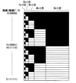
図7は、上記の間引き走査の一例を模式的に表したものである。図7(A)に示したように、1フレーム期間が7つのサブブロックSB1〜SB7で分割され、各サブブロックSB1〜SB7が図8に示した3つのサブフィールドで構成されている。図7(B)〜(H)に示したように、各走査線1〜7はサブブロック単位で間引き走査されている。さらに、全てのサブブロックSB1〜SB7で各走査線1〜7が間引き走査されることにより、各サブフィールドに対応するビットに従って、各走査線1〜7に接続された画素がオンまたはオフされる。
FIG. 7 schematically shows an example of the thinning scanning. As shown in FIG. 7A, one frame period is divided into seven sub-blocks SB1 to SB7, and each sub-block SB1 to SB7 is composed of the three sub-fields shown in FIG. As shown in FIGS. 7B to 7H, the
図7に記載の階調表示法では、転送速度がサブブロックごとに均一となっており、しかも、従来の階調表示法よりも、転送速度を大幅に低減することができる。そのため、階調数が、最小ビットの転送速度に律束されることがないので、階調数を容易に増やすことができる。しかし、図7に記載の階調表示法では、階調数が走査線の数によって制限を受ける。そのため、階調数を増やすために、走査線の数を増やさなければならなくなる事態が起こり得る。 In the gradation display method shown in FIG. 7, the transfer speed is uniform for each sub-block, and the transfer speed can be significantly reduced as compared with the conventional gradation display method. Therefore, since the number of gradations is not limited by the transfer rate of the minimum bit, the number of gradations can be easily increased. However, in the gradation display method shown in FIG. 7, the number of gradations is limited by the number of scanning lines. Therefore, there may occur a situation where the number of scanning lines has to be increased in order to increase the number of gradations.
本技術はかかる問題点に鑑みてなされたものであり、その第1の目的は、走査線の数を増やさなくても、階調数を増やすことの可能な駆動回路およびそれを備えた表示装置を提供することにある。また、第2の目的は、走査線の数を増やさなくても、階調数を増やすことの可能な表示装置の駆動方法を提供することにある。 The present technology has been made in view of such problems, and a first object thereof is a drive circuit capable of increasing the number of gradations without increasing the number of scanning lines, and a display device including the drive circuit. Is to provide. A second object is to provide a driving method of a display device capable of increasing the number of gradations without increasing the number of scanning lines.
本技術による駆動回路は、電気光学素子を含むメモリ内蔵の画素が行列状に配置され、画素行ごとに走査線が設けられた表示装置における各画素を駆動する回路である。駆動回路は、分割部と、オンオフ期間制御部とを含んでいる。分割部は、階調データの各ビットに対応し、かつ対応ビットの重みに応じた期間となる複数のサブフィールドからなる複数のサブブロックで1フレーム期間を分割するようになっている。オンオフ期間制御部は、各サブフィールドに対応するビットに従って画素の電気光学素子をオンまたはオフすることで、1フレーム期間中のオン期間またはオフ期間の割合を制御するようになっている。オンオフ期間制御部は、さらに、サブブロック単位で、当該サブブロックに含まれるサブフィールドの数より1だけ少ない数の走査線を選択するとともに、選択した一の走査線を再度、同一サブブロック期間中に選択するようになっている。 The drive circuit according to the present technology is a circuit that drives each pixel in a display device in which pixels with built-in memory including electro-optic elements are arranged in a matrix and a scanning line is provided for each pixel row. The drive circuit includes a dividing unit and an on / off period control unit. The dividing unit divides one frame period by a plurality of sub-blocks that correspond to each bit of the gradation data and have a plurality of sub-fields having a period corresponding to the weight of the corresponding bit. The on / off period control unit controls the ratio of the on period or the off period in one frame period by turning on or off the electro-optic element of the pixel according to the bit corresponding to each subfield. The on / off period control unit further selects, in subblock units, the number of scanning lines that is one less than the number of subfields included in the subblock, and again selects the selected one scanning line during the same subblock period. To choose.
本技術による表示装置は、電気光学素子を含むメモリ内蔵の画素が行列状に配置され、画素行ごとに走査線が設けられた表示領域と、各画素を駆動する駆動回路とを備えている。この表示装置において、駆動回路は、上記の分割部と同一の構成要素の分割部と、上記のオンオフ期間制御部と同一の構成要素のオンオフ期間制御部とを備えている。 A display device according to an embodiment of the present technology includes a display area in which pixels having a built-in memory including electro-optic elements are arranged in a matrix, a scanning line is provided for each pixel row, and a drive circuit that drives each pixel. In this display device, the drive circuit includes a division unit having the same components as the division unit and an on / off period control unit having the same components as the on / off period control unit.
本技術による表示装置の駆動方法は、電気光学素子を含むメモリ内蔵の画素が行列状に配置され、画素行ごとに走査線が設けられた表示装置の駆動方法である。この駆動方法は、以下の3つのステップを含んでいる。
(A)階調データの各ビットに対応し、かつ対応ビットの重みに応じた期間となる複数のサブフィールドからなる複数のサブブロックで1フレーム期間を分割する分割ステップ
(B)各サブフィールドに対応するビットに従って画素の電気光学素子をオンまたはオフすることで、1フレーム期間中のオン期間またはオフ期間の割合を制御するオンオフ期間制御ステップ
(C)オンオフ期間制御ステップにおいて、サブブロック単位で、当該サブブロックに含まれるサブフィールドの数より1だけ少ない数の走査線を選択するとともに、選択した一の走査線を再度、同一サブブロック期間中に選択するステップ
The driving method of the display device according to the present technology is a driving method of the display device in which pixels with built-in memory including electro-optic elements are arranged in a matrix and a scanning line is provided for each pixel row. This driving method includes the following three steps.
(A) Dividing step of dividing one frame period by a plurality of sub-blocks composed of a plurality of sub-fields corresponding to each bit of gradation data and having a period corresponding to the weight of the corresponding bit. (B) In each sub-field In an on / off period control step (C) on / off period control step for controlling the ratio of the on period or the off period in one frame period by turning on or off the electro-optic element of the pixel according to the corresponding bit, Selecting a number of scanning lines that is one less than the number of subfields included in the sub-block and selecting the selected scanning line again during the same sub-block period
本技術による駆動回路、表示装置、および表示装置の駆動方法では、サブブロック単位で、当該サブブロックに含まれるサブフィールドの数より1だけ少ない数の走査線が選択されとともに、選択した一の走査線が再度、同一サブブロック期間中に選択される。これにより、サブブロックの期間よりも短い期間で、再選択する直前のサブフィールドに対応するビットとは異なるビットに従ったオンオフ駆動に切り換えることができる。 In the driving circuit, the display device, and the driving method of the display device according to the present technology, the number of scanning lines that is smaller by one than the number of subfields included in the subblock is selected for each subblock, and one selected scan is performed. The line is again selected during the same sub-block period. Thereby, it is possible to switch to on / off driving according to a bit different from the bit corresponding to the subfield immediately before reselection in a period shorter than the period of the subblock.
本技術による駆動回路、表示装置、および表示装置の駆動方法によれば、サブブロックの期間よりも短い期間で、再選択する直前のサブフィールドに対応するビットとは異なるビットに従ったオンオフ駆動に切り換えることができるようにしたので、走査線の数を増やさなくても、階調数を増やすことができる。 According to the driving circuit, the display device, and the driving method of the display device according to the present technology, on-off driving according to a bit different from the bit corresponding to the subfield immediately before the reselection is performed in a period shorter than the subblock period. Since switching can be performed, the number of gradations can be increased without increasing the number of scanning lines.
以下、発明を実施するための形態について、図面を参照して詳細に説明する。なお、説明は以下の順序で行う。
1.実施の形態(表示装置)
2.変形例(表示装置)
DESCRIPTION OF EMBODIMENTS Hereinafter, embodiments for carrying out the invention will be described in detail with reference to the drawings. The description will be given in the following order.
1. Embodiment (display device)
2. Modified example (display device)
<1.実施の形態>
[構成]
図1は、本技術による一実施の形態に係る表示装置1の概略構成を表したものである。この表示装置1は、表示パネル10と、表示パネル10を駆動する周辺回路20とを備えている。
<1. Embodiment>
[Constitution]
FIG. 1 illustrates a schematic configuration of a
(表示パネル10)
表示パネル10は、行方向に延在する複数の走査線WSLと、列方向に延在する複数のデータ線DTLとを有しており、走査線WSLとデータ線DTLとが互いに交差する箇所に対応して画素11を有している。表示パネル10内の複数の画素11は、表示パネル10の画素領域10A全面に渡って行方向および列方向に2次元配置されている。画素11は、表示パネル10上の画面を構成する最小単位の点に対応するものである。表示パネル10がカラー表示パネルである場合には、画素11は、例えば赤、緑または青などの単色の光を発する副画素に相当し、表示パネル10がモノクロ表示パネルである場合には、画素11は、単色光(例えば白色光)を発する画素に相当する。
(Display panel 10)
The
画素11は、図示しないが、電気光学素子を含むメモリ内蔵の画素である。電気光学素子の種類としては、例えば、液晶セルや、有機EL(Electro Luminescence)セルなどが挙げられる。メモリの種類としては、例えば、SRAM(Static Random Access Memory)やDRAM(Dynamic Random Access Memory)などが挙げられる。画素11は、対応する1本の走査線WSLが選択されたとき、対応するデータ線DTLに供給された信号データ(ビット)の書込みに応じて発光状態または消光状態となり、その後、当該走査線WSLが非選択となっても、書込みによる発光状態または消光状態が継続するようになっている。そのため、周辺回路20は、画素11が発光状態となっている期間(点灯期間)、または画素11が消光状態となっている期間(消灯期間)の、1フレーム期間における割合を制御することにより、階調表示を実現している。
Although not shown, the pixel 11 is a pixel with a built-in memory including an electro-optical element. Examples of the electro-optical element include a liquid crystal cell and an organic EL (Electro Luminescence) cell. Examples of the memory type include SRAM (Static Random Access Memory) and DRAM (Dynamic Random Access Memory). When one corresponding scanning line WSL is selected, the pixel 11 enters a light emitting state or a quenching state according to the writing of the signal data (bit) supplied to the corresponding data line DTL, and then the scanning line WSL. Even if is not selected, the light emission state or the extinction state by writing continues. Therefore, the
画素11の点灯期間または消灯期間の単位として「サブフィールド」という概念がある。「サブフィールド」とは、画素11の階調を規定する階調データの各ビットに対応し、かつ当該対応ビットの重みに応じた期間の単位を指している。一般に、例えば、5ビットからなる階調データによって32階調を表現する場合、例えば、図5に示したように、例えば数ms幅の1ビットのデータを単位として、期間の比が1:2:4:8:16の5つのデータが用意され、これら5つのデータの組み合わせにより32階調が表現される。上記の階調表示法では、図6(A)に示したように、階調データの各ビット(1bit〜5bit)に対応し、かつ対応ビットの重みに応じた期間となるサブフィールドSF1〜SF5で、信号データが規定される。 There is a concept of “subfield” as a unit of the lighting period or extinguishing period of the pixel 11. The “subfield” refers to a unit of a period corresponding to each bit of the gradation data defining the gradation of the pixel 11 and corresponding to the weight of the corresponding bit. In general, for example, when 32 gradations are expressed by gradation data consisting of 5 bits, for example, as shown in FIG. 5, the ratio of periods is 1: 2 in units of 1-bit data having a width of several ms, for example. : 5: 8: 16 are prepared, and 32 gradations are expressed by a combination of these five data. In the above gradation display method, as shown in FIG. 6A, subfields SF1 to SF5 correspond to each bit (1 bit to 5 bits) of the gradation data and have a period corresponding to the weight of the corresponding bit. Thus, the signal data is defined.
本実施の形態では、複数のサブフィールドを1つのサブブロックにまとめ、複数のサブブロックで1フレーム期間を分割し、サブブロック単位で走査線を間引き走査する階調表示法が適用されている。 In this embodiment, a gradation display method is applied in which a plurality of subfields are combined into one subblock, one frame period is divided by the plurality of subblocks, and scanning lines are thinned out in units of subblocks.
図2は、上記の階調表示法の一例を模式的に表したものである。図2(A)に示したように、1フレーム期間が7つのサブブロックSB1〜SB7で分割され、各サブブロックSB1〜SB7が図3に示した4つのサブフィールドで構成されている。各サブフィールドは、階調データの各ビットに対応し、かつ対応ビットの重みに応じた期間となっている。具体的には、期初のサブフィールドは、階調データの1ビット目に対応しており、期初のサブフィールドの期間は、1ビット目の重みに対応して幅0.5となっている。2番目のサブフィールドは、階調データの2ビット目に対応しており、2番目のサブフィールドの期間は、2ビット目の重みに対応して幅1となっている。3番目のサブフィールドは、階調データの4ビット目に対応しており、3番目のサブフィールドの期間は、4ビット目の重みに対応して幅3.5となっている。4番目のサブフィールドは、階調データの3ビット目に対応しており、4番目のサブフィールドの期間は、3ビット目の重みに対応して幅2となっている。各サブブロックSB1〜SB7において、幅の最も大きなサブフィールドが、4番目ではなく、3番目に配置されている。 FIG. 2 schematically shows an example of the gradation display method. As shown in FIG. 2A, one frame period is divided into seven sub-blocks SB1 to SB7, and each sub-block SB1 to SB7 is composed of the four sub-fields shown in FIG. Each subfield has a period corresponding to each bit of the gradation data and corresponding to the weight of the corresponding bit. Specifically, the initial subfield corresponds to the first bit of the gradation data, and the initial subfield period has a width of 0.5 corresponding to the weight of the first bit. The second subfield corresponds to the second bit of the gradation data, and the period of the second subfield has a width of 1 corresponding to the weight of the second bit. The third subfield corresponds to the fourth bit of the gradation data, and the period of the third subfield has a width of 3.5 corresponding to the weight of the fourth bit. The fourth subfield corresponds to the third bit of the gradation data, and the period of the fourth subfield has a width of 2 corresponding to the weight of the third bit. In each of the sub-blocks SB1 to SB7, the subfield having the largest width is arranged in the third, not the fourth.
図2(B)〜(H)に示したように、各走査線1〜7はサブブロック単位で間引き走査されている。さらに、全てのサブブロックSB1〜SB7で各走査線1〜7が間引き走査されることにより、各サブフィールドに対応するビットに従って、各走査線1〜7に接続された画素がオンまたはオフされる。各サブブロックSB1〜SB7での走査では、サブブロックSB1〜SB7ごとに、当該サブブロックに含まれるサブフィールドの数より1だけ少ない数の走査線が選択されるとともに、選択した一の走査線が再度、同一サブブロック期間中に選択されている。間引き走査の走査速度は、走査線の選択本数に依っており、全てのサブブロックSB1〜SB7において互いに等しくなっている。また、走査線の再選択のタイミングは、常に、幅の最も大きなサブフィールドの開始のタイミングに一致(または同期)している。
As shown in FIGS. 2B to 2H, the
例えば、サブブロックSB1においては、3本の走査線1,5,7が選択されるとともに、選択された3本の走査線1,5,7のうち走査線1が再度、サブブロックSB1期間中に選択されている。また、例えば、サブブロックSB2においては、3本の走査線1,2,6が選択されるとともに、選択された3本の走査線1,2,6のうち走査線2が再度、サブブロックSB2期間中に選択されている。また、例えば、サブブロックSB3においては、3本の走査線2,3,7が選択されるとともに、選択された3本の走査線2,3,7のうち走査線3が再度、サブブロックSB3期間中に選択されている。また、例えば、サブブロックSB4においては、3本の走査線1,3,4が選択されるとともに、選択された3本の走査線1,3,4のうち走査線4が再度、サブブロックSB4期間中に選択されている。また、例えば、サブブロックSB5においては、3本の走査線2,4,5が選択されるとともに、選択された3本の走査線2,4,5のうち走査線5が再度、サブブロックSB5期間中に選択されている。また、例えば、サブブロックSB6においては、3本の走査線3,5,6が選択されるとともに、選択された3本の走査線3,5,6のうち走査線6が再度、サブブロックSB6期間中に選択されている。また、例えば、サブブロックSB7においては、3本の走査線4,6,7が選択されるとともに、選択された3本の走査線4,6,7のうち走査線7が再度、サブブロックSB7期間中に選択されている。
For example, in the sub-block SB1, three
走査線の再選択のタイミングは、いずれのサブブロックSB1〜SB7においても、3番目のサブフィールドの開始のタイミングに一致(または同期)している。また、再選択される走査線は、いずれのサブブロックSB1〜SB7においても、1番目に選択され、その後、3番目に再選択されている。ここで、走査線が再度、同一サブフレーム期間中に選択されたときに、当初のビットとは異なるビットが画素に書き込まれる。つまり、再選択によってオンオフ駆動の切り換えがなされる区間の最短期間は、図2(B)〜(H)に示したように、期初のサブフィールドおよび2番目のサブフィールドのそれぞれの期間の合計に相当する。なお、図2(B)〜(H)では、再選択によってオンオフ駆動の切り換えがなされる区間のビットが、常に1(白)となっているが、図示しないが、0(黒)となっていてもよい。 The scanning line reselection timing coincides (or synchronizes) with the start timing of the third subfield in any of the sub-blocks SB1 to SB7. Further, the reselected scanning line is selected first in any of the sub-blocks SB1 to SB7, and then reselected third. Here, when the scanning line is selected again during the same subframe period, a bit different from the original bit is written into the pixel. In other words, as shown in FIGS. 2B to 2H, the shortest period in which the on / off drive is switched by reselection is the sum of the periods of the initial subfield and the second subfield. Equivalent to. In FIGS. 2B to 2H, the bit in the section where the on / off drive is switched by reselection is always 1 (white), but it is 0 (black) although not shown. May be.
現フレームの信号データの各画素行における書込みは、各サブブロックSB1〜SB7の期初に各走査線が順次選択されるのに対応して開始される。例えば、サブブロックSB1において、走査線が1,7,1,5の順にまびき選択されたときに、走査線1の選択に対応して現フレームの信号データが書き込まれ、走査線5,7の選択に対応して前フレームの信号データが書きこまれる。
The writing of the signal data of the current frame in each pixel row is started in response to the sequential selection of each scanning line at the beginning of each sub-block SB1 to SB7. For example, in the sub-block SB1, when the scanning lines are selected in the order of 1, 7, 1, 5, the signal data of the current frame is written in response to the selection of the
(周辺回路20)
次に、周辺回路20の構成についての説明を行う。周辺回路20は、例えば、図1に示したように、変換回路30、コントローラ40、垂直駆動回路50および水平駆動回路60を有している。
(Peripheral circuit 20)
Next, the configuration of the
コントローラ40は、図示しない上位装置から供給される同期信号20Bから、変換回路30、垂直駆動回路50、および水平駆動回路60の動作タイミングを制御する制御信号40A,40B,40Cを生成するものである。同期信号20Bとしては、例えば、垂直同期信号、水平同期信号、ドットクロック信号などが挙げられる。制御信号40A,40B,40Cとしては、例えば、クロック信号、ラッチ信号、フレーム開始信号、サブフィールド開始信号などが挙げられる。
The
変換回路30は、例えば、図4に示したように、フレームメモリ31、書込回路32、読出回路33およびデコーダ34を含んでいる。フレームメモリ31は、少なくとも表示領域10Aの解像度よりも多い記憶容量を有する映像表示用メモリであり、例えば、行アドレスと、列アドレスと、行アドレスおよび列アドレスと関連付けられた各画素11の階調データとを記憶することができるようになっている。書込回路32は、同期信号20B利用して、映像信号20Aの書込アドレスWadを生成するとともに、同期信号20Bに同期してフレームメモリ31に出力するようになっている。書込みアドレスWadは、例えば、行アドレスおよび列アドレスを含んでいる。読出回路33は、制御信号20Cに基づいて、読出アドレスRadを生成し、フレームメモリ31に出力するようになっている。デコーダ34は、フレームメモリ31から出力された階調データを信号データ30Aとして出力するようになっている。
The
垂直駆動回路50は、制御信号40Cから特定されるアドレスデータに基づいて、各画素11を行単位で選択するための走査パルスを走査線WSLに出力するようになっている。垂直駆動回路50は、例えば、図2(B)〜(H)に示したように、1フレーム期間を7つのサブブロックSB1〜SB7で分割し、各サブブロックSB1〜SB7を図3に示した4つのサブフィールドで分割している。垂直駆動回路50は、例えば、図2(B)〜(H)に示したように、各走査線1〜7をサブブロック単位で間引き走査するようになっている。垂直駆動回路50は、各サブブロックSB1〜SB7での走査において、サブブロックSB1〜SB7ごとに、当該サブブロックに含まれるサブフィールドの数より1だけ少ない数の走査線を選択するとともに、選択した一の走査線を再度、同一サブブロック期間中に選択するようになっている。
The
垂直駆動回路50は、走査線の再選択のタイミングを、いずれのサブブロックSB1〜SB7においても、3番目のサブフィールドの開始のタイミングに一致(または同期)させている。また、垂直駆動回路50は、再選択される走査線を、いずれのサブブロックSB1〜SB7においても、1番目に選択し、その後、3番目に再選択するようになっている。
The
水平駆動回路60は、制御信号40Bと、信号データ30Aとに基づいて、各サブフィールドに対応するビットに従って画素11の電気光学素子をオンまたはオフすることで、1F中のオン期間またはオフ期間の割合を段階的に制御するようになっている。水平駆動回路60は、例えば、図2(A)に示したように、各サブブロックSB1〜SB7のサブブフィールドに対応する階調データを各データ線DTLに出力するようになっている。水平駆動回路60は、垂直駆動回路50が走査線を再度、同一サブフレーム期間中に選択したときに、当初のビットとは異なるビットを、データ線DTLを介して画素に書き込むようになっている。
The
[効果]
次に、従来の一般的なデジタル駆動と対比しつつ、本実施の形態の表示装置1の効果について説明する。
[effect]
Next, the effects of the
従来の一般的なPWMのデジタル駆動では、5ビット(32階調)の場合を例にとると、例えば、図5に示したような階調表示法が用いられる。具体的には、図5に示したように、例えば数ms幅の1ビットのデータを単位として、期間の比が1:2:4:8:16の5つのデータを用意し、これら5つのデータの組み合わせにより32階調が表現される。 In the conventional general PWM digital drive, for example, in the case of 5 bits (32 gradations), a gradation display method as shown in FIG. 5 is used. Specifically, as shown in FIG. 5, for example, five data having a period ratio of 1: 2: 4: 8: 16 are prepared in units of 1-bit data having a width of several ms. 32 gradations are expressed by the combination of data.
図6は、従来の一般的なデジタル駆動における順次走査の信号データと、走査線に印加される選択パルスとの関係を表したものである。ここでは、説明の都合上、走査線が3本の場合を示している。図6からわかるように、従来の一般的なデジタル駆動の表示装置では、階調データの各ビット(本例では、1bit〜5bit)に対応し、かつ対応ビットの重みに応じた期間となるサブフィールドSF1〜SF5で1フレーム期間(1F)が分割されている。そして、各サブフィールドSF1〜SF5に対応するビットに従って画素の電気光学素子がオンまたはオフされることで、1F中のオン期間またはオフ期間の割合が段階的に制御される。さらに、走査線を介した画素へのデータ書込みは、サブフィールドSF1〜SF5ごとに線順次走査で行われる。 FIG. 6 shows the relationship between sequential scanning signal data in conventional general digital driving and a selection pulse applied to a scanning line. Here, for convenience of explanation, a case where there are three scanning lines is shown. As can be seen from FIG. 6, in the conventional general digital drive display device, the sub-corresponding to each bit of the gradation data (1 bit to 5 bit in this example) and corresponding to the weight of the corresponding bit. One frame period (1F) is divided by fields SF1 to SF5. Then, the ratio of the on period or the off period in 1F is controlled stepwise by turning on or off the electro-optic elements of the pixels according to the bits corresponding to the subfields SF1 to SF5. Further, data writing to the pixels via the scanning lines is performed by line-sequential scanning for each of the subfields SF1 to SF5.
しかし、上記の階調表示法では、最小ビット(1bit)の転送速度で、信号データの転送速度が律束されるので、階調数を容易に増やすことができない。そこで、例えば、複数のサブフィールドを1つのサブブロックにまとめ、複数のサブブロックで1フレーム期間を分割し、サブブロック単位で走査線を間引き走査することが考えられる。 However, in the above gradation display method, the transfer rate of signal data is regulated by the transfer rate of the minimum bit (1 bit), and therefore the number of gradations cannot be easily increased. Therefore, for example, it is conceivable that a plurality of subfields are combined into one subblock, one frame period is divided by the plurality of subblocks, and scanning lines are thinned out in units of subblocks.
図7は、上記の間引き走査の一例を模式的に表したものである。図7(A)に示したように、1フレーム期間が7つのサブブロックSB1〜SB7で分割され、各サブブロックSB1〜SB7が図8に示した3つのサブフィールドで構成されている。図7(B)〜(H)に示したように、各走査線1〜7はサブブロック単位で間引き走査されている。さらに、全てのサブブロックSB1〜SB7で各走査線1〜7が間引き走査されることにより、各サブフィールドに対応するビットに従って、各走査線1〜7に接続された画素がオンまたはオフされる。
FIG. 7 schematically shows an example of the thinning scanning. As shown in FIG. 7A, one frame period is divided into seven sub-blocks SB1 to SB7, and each sub-block SB1 to SB7 is composed of the three sub-fields shown in FIG. As shown in FIGS. 7B to 7H, the
図7に記載の階調表示法では、転送速度がサブブロックごとに均一となっており、しかも、従来の階調表示法よりも、転送速度を大幅に低減することができる。そのため、階調数が、最小ビットの転送速度に律束されることがないので、階調数を容易に増やすことができる。しかし、図7に記載の階調表示法では、階調数が走査線の数によって制限を受ける。そのため、階調数を増やすために、走査線の数を増やさなければならなくなる事態が起こり得る。 In the gradation display method shown in FIG. 7, the transfer speed is uniform for each sub-block, and the transfer speed can be significantly reduced as compared with the conventional gradation display method. Therefore, since the number of gradations is not limited by the transfer rate of the minimum bit, the number of gradations can be easily increased. However, in the gradation display method shown in FIG. 7, the number of gradations is limited by the number of scanning lines. Therefore, there may occur a situation where the number of scanning lines has to be increased in order to increase the number of gradations.
一方、本実施の形態では、サブブロック単位で、当該サブブロックに含まれるサブフィールドの数より1だけ少ない数の走査線が選択されとともに、選択した一の走査線が再度、同一サブブロック期間中に選択される。これにより、サブブロックの期間よりも短い期間で、再選択する直前のサブフィールドに対応するビットとは異なるビットに従ったオンオフ駆動に切り換えることができる。その結果、走査線の数を増やさなくても、階調数を増やすことができる。 On the other hand, in the present embodiment, the number of scanning lines that is one less than the number of subfields included in the subblock is selected in units of subblocks, and the selected one scanning line is again in the same subblock period. Selected. Thereby, it is possible to switch to on / off driving according to a bit different from the bit corresponding to the subfield immediately before reselection in a period shorter than the period of the subblock. As a result, the number of gradations can be increased without increasing the number of scanning lines.
<2.変形例>
以上、実施の形態を挙げて本技術を説明したが、本技術は上記実施の形態に限定されるものではなく、種々変形が可能である。
<2. Modification>
While the present technology has been described with reference to the embodiment, the present technology is not limited to the above-described embodiment, and various modifications can be made.
例えば、上記実施の形態では、走査線の再選択は、1サブフレーム期間中に1回だけとなっていたが、例えば、図7、図8に示したように、1サブフレーム期間中に2回となっていてもよい。走査線の再選択を1サブフレーム期間中に2回行った場合には、走査線の再選択を行わなかった場合と比べてビット数を2つ増やすことができる。 For example, in the above-described embodiment, scanning line reselection is performed only once during one subframe period. For example, as shown in FIGS. It may be times. When scanning line reselection is performed twice during one subframe period, the number of bits can be increased by two compared to when scanning line reselection is not performed.
また、上記実施の形態等では、変換回路30、垂直駆動回路50および水平駆動回路60の駆動をコントローラ40が制御していたが、他の回路がこれらの駆動を制御するようにしてもよい。また、変換回路30、垂直駆動回路50および水平駆動回路60の制御は、ハードウェア(回路)で行われていてもよいし、ソフトウェア(プログラム)で行われていてもよい。
In the above embodiment and the like, the
1…表示装置、10…表示パネル、10A…画素領域、11…画素、20…周辺回路、20A…映像信号、20B…同期信号、30…変換回路、30A…信号データ、31…フレームメモリ、32…書込回路、33…読出回路、34…デコーダ、40…コントローラ、40A,40B,40C…制御信号、50…垂直駆動回路、60…水平駆動回路、DTL…データ線、WSL…走査線。
DESCRIPTION OF
Claims (4)
階調データの各ビットに対応し、かつ対応ビットの重みに応じた期間となる複数のサブフィールドからなる複数のサブブロックで1フレーム期間を分割する分割部と、
各サブフィールドに対応するビットに従って画素の電気光学素子をオンまたはオフすることで、1フレーム期間中のオン期間またはオフ期間の割合を制御するオンオフ期間制御部と
を備え、
前記オンオフ期間制御部は、前記サブブロック単位で、当該サブブロックに含まれるサブフィールドの数より1だけ少ない数の走査線を選択するとともに、選択した一の走査線を再度、同一サブブロック期間中に選択するようになっている
駆動回路。 A drive circuit that drives each pixel in a display device in which pixels with built-in memory including electro-optic elements are arranged in a matrix and a scanning line is provided for each pixel row,
A dividing unit that divides one frame period by a plurality of sub-blocks that include a plurality of sub-fields that correspond to each bit of gradation data and have a period according to the weight of the corresponding bit;
An on / off period control unit for controlling the ratio of the on period or the off period in one frame period by turning on or off the electro-optic element of the pixel according to the bit corresponding to each subfield,
The on / off period control unit selects one scan line less than the number of subfields included in the subblock in the subblock unit, and again selects the selected one scan line during the same subblock period. The drive circuit that is supposed to be selected.
請求項1に記載の駆動回路。 The drive circuit according to claim 1, wherein the on / off period control unit writes a bit different from an initial bit to a pixel when the selected one scanning line is selected again during the same sub-block period.
各画素を駆動する駆動回路と
を備え、
前記駆動回路は、
階調データの各ビットに対応し、かつ対応ビットの重みに応じた期間となる複数のサブフィールドからなる複数のサブブロックで1フレーム期間を分割する分割部と、
各サブフィールドに対応するビットに従って画素の電気光学素子をオンまたはオフすることで、1フレーム期間中のオン期間またはオフ期間の割合を制御するオンオフ期間制御部と
を有し、
前記オンオフ期間制御部は、前記サブブロック単位で、当該サブブロックに含まれるサブフィールドの数より1だけ少ない数の走査線を選択するとともに、選択した一の走査線を再度、同一サブブロック期間中に選択するようになっている
表示装置。 A display area in which pixels with a built-in memory including electro-optic elements are arranged in a matrix and a scanning line is provided for each pixel row;
A drive circuit for driving each pixel, and
The drive circuit is
A dividing unit that divides one frame period by a plurality of sub-blocks that include a plurality of sub-fields that correspond to each bit of gradation data and have a period according to the weight of the corresponding bit;
An on / off period control unit that controls the ratio of the on period or the off period in one frame period by turning on or off the electro-optic element of the pixel according to the bit corresponding to each subfield;
The on / off period control unit selects one scan line less than the number of subfields included in the subblock in the subblock unit, and again selects the selected one scan line during the same subblock period. A display device that is adapted to be selected.
階調データの各ビットに対応し、かつ対応ビットの重みに応じた期間となる複数のサブフィールドからなる複数のサブブロックで1フレーム期間を分割する分割ステップと、
各サブフィールドに対応するビットに従って画素の電気光学素子をオンまたはオフすることで、1フレーム期間中のオン期間またはオフ期間の割合を制御するオンオフ期間制御ステップと
を含み、
前記オンオフ期間制御ステップにおいて、前記サブブロック単位で、当該サブブロックに含まれるサブフィールドの数より1だけ少ない数の走査線を選択するとともに、選択した一の走査線を再度、同一サブブロック期間中に選択する
表示装置の駆動方法。 A method of driving a display device in which pixels with built-in memory including electro-optic elements are arranged in a matrix and a scanning line is provided for each pixel row,
A division step of dividing one frame period by a plurality of sub-blocks composed of a plurality of sub-fields corresponding to each bit of gradation data and having a period according to the weight of the corresponding bit;
An on / off period control step of controlling a ratio of an on period or an off period in one frame period by turning on or off an electro-optic element of a pixel according to a bit corresponding to each subfield,
In the on / off period control step, the number of scanning lines smaller by one than the number of subfields included in the subblock is selected for each subblock, and the selected one scanning line is again selected in the same subblock period. Select a display device drive method.
Priority Applications (2)
| Application Number | Priority Date | Filing Date | Title |
|---|---|---|---|
| JP2011189927A JP2013050680A (en) | 2011-08-31 | 2011-08-31 | Driving circuit, display, and method of driving the display |
| US13/567,666 US9858852B2 (en) | 2011-08-31 | 2012-08-06 | Driving circuit, display, and method of driving the display |
Applications Claiming Priority (1)
| Application Number | Priority Date | Filing Date | Title |
|---|---|---|---|
| JP2011189927A JP2013050680A (en) | 2011-08-31 | 2011-08-31 | Driving circuit, display, and method of driving the display |
Publications (2)
| Publication Number | Publication Date |
|---|---|
| JP2013050680A true JP2013050680A (en) | 2013-03-14 |
| JP2013050680A5 JP2013050680A5 (en) | 2014-09-25 |
Family
ID=47743053
Family Applications (1)
| Application Number | Title | Priority Date | Filing Date |
|---|---|---|---|
| JP2011189927A Pending JP2013050680A (en) | 2011-08-31 | 2011-08-31 | Driving circuit, display, and method of driving the display |
Country Status (2)
| Country | Link |
|---|---|
| US (1) | US9858852B2 (en) |
| JP (1) | JP2013050680A (en) |
Cited By (1)
| Publication number | Priority date | Publication date | Assignee | Title |
|---|---|---|---|---|
| CN116386519A (en) * | 2023-05-09 | 2023-07-04 | 集创北方(成都)科技有限公司 | LED driving circuit, driving method, chip and display device |
Families Citing this family (4)
| Publication number | Priority date | Publication date | Assignee | Title |
|---|---|---|---|---|
| TWI633532B (en) * | 2017-07-24 | 2018-08-21 | 中國大陸商晶門科技(深圳)有限公司 | Method and apparatus of grayscale image generation in monochrome display |
| US10643519B2 (en) | 2017-07-24 | 2020-05-05 | Solomon Systech (Shenzhen) Limited | Method and apparatus of grayscale image generation in monochrome display |
| KR102395792B1 (en) * | 2017-10-18 | 2022-05-11 | 삼성디스플레이 주식회사 | Display device and driving method thereof |
| JP2022010676A (en) * | 2020-06-29 | 2022-01-17 | セイコーエプソン株式会社 | Circuit arrangement, electro-optical device, and electronic apparatus |
Citations (4)
| Publication number | Priority date | Publication date | Assignee | Title |
|---|---|---|---|---|
| JP2004004501A (en) * | 2002-04-09 | 2004-01-08 | Sharp Corp | Driving device for electro-optical device, display device using the same, driving method for the same, and method for setting weight of the same |
| JP2006030946A (en) * | 2004-06-14 | 2006-02-02 | Sharp Corp | Display apparatus |
| JP2008058921A (en) * | 2006-08-30 | 2008-03-13 | Samsung Sdi Co Ltd | Driving method of organic electric field light emitting display apparatus |
| US20080191977A1 (en) * | 2007-02-12 | 2008-08-14 | Samsung Electronics Co., Ltd. | Method and apparatus for digitally driving an AMOLED |
Family Cites Families (9)
| Publication number | Priority date | Publication date | Assignee | Title |
|---|---|---|---|---|
| US5614924A (en) * | 1994-06-01 | 1997-03-25 | Sharp Kabushiki Kaisha | Ferroelectric liquid crystal display device and a driving method of effecting gradational display therefor |
| JP3834086B2 (en) | 1995-11-06 | 2006-10-18 | シャープ株式会社 | Matrix type display device and driving method thereof |
| KR100289534B1 (en) * | 1998-09-16 | 2001-05-02 | 김순택 | A method for displaying gray scale of PDP and an apparatus for the same |
| JP3524778B2 (en) | 1998-10-06 | 2004-05-10 | シャープ株式会社 | Operation method of display device |
| TW536689B (en) * | 2001-01-18 | 2003-06-11 | Sharp Kk | Display, portable device, and substrate |
| KR100712126B1 (en) * | 2005-01-24 | 2007-04-27 | 삼성에스디아이 주식회사 | Liquid Crystal Display Device |
| JP5002914B2 (en) | 2005-06-10 | 2012-08-15 | ソニー株式会社 | Display device and driving method of display device |
| JP4985020B2 (en) * | 2007-03-27 | 2012-07-25 | セイコーエプソン株式会社 | Liquid crystal device, driving method thereof, and electronic apparatus |
| JP2010026086A (en) * | 2008-07-16 | 2010-02-04 | Seiko Epson Corp | Driving device and method for electrooptical device, electrooptical device, and electronic equipment |
-
2011
- 2011-08-31 JP JP2011189927A patent/JP2013050680A/en active Pending
-
2012
- 2012-08-06 US US13/567,666 patent/US9858852B2/en active Active
Patent Citations (4)
| Publication number | Priority date | Publication date | Assignee | Title |
|---|---|---|---|---|
| JP2004004501A (en) * | 2002-04-09 | 2004-01-08 | Sharp Corp | Driving device for electro-optical device, display device using the same, driving method for the same, and method for setting weight of the same |
| JP2006030946A (en) * | 2004-06-14 | 2006-02-02 | Sharp Corp | Display apparatus |
| JP2008058921A (en) * | 2006-08-30 | 2008-03-13 | Samsung Sdi Co Ltd | Driving method of organic electric field light emitting display apparatus |
| US20080191977A1 (en) * | 2007-02-12 | 2008-08-14 | Samsung Electronics Co., Ltd. | Method and apparatus for digitally driving an AMOLED |
Cited By (2)
| Publication number | Priority date | Publication date | Assignee | Title |
|---|---|---|---|---|
| CN116386519A (en) * | 2023-05-09 | 2023-07-04 | 集创北方(成都)科技有限公司 | LED driving circuit, driving method, chip and display device |
| CN116386519B (en) * | 2023-05-09 | 2023-10-24 | 集创北方(成都)科技有限公司 | LED driving circuit, driving method, chip and display device |
Also Published As
| Publication number | Publication date |
|---|---|
| US9858852B2 (en) | 2018-01-02 |
| US20130050299A1 (en) | 2013-02-28 |
Similar Documents
| Publication | Publication Date | Title |
|---|---|---|
| JP4968857B2 (en) | Pixel driving apparatus and pixel driving method | |
| JP5395328B2 (en) | Display device | |
| JP5046355B2 (en) | Display control apparatus and display control method for video signal | |
| KR100858614B1 (en) | Organic light emitting display and driving method the same | |
| JP5849538B2 (en) | Driving circuit, display device, and driving method of display device | |
| KR100826508B1 (en) | Method for digital driving active matrix organic light emitting diodes and apparutus thereof | |
| US7479972B2 (en) | Display device | |
| JP2013050679A (en) | Driving circuit, display, and method of driving the display | |
| JP2006276410A (en) | Apparatus and method for driving light-emitting display panel | |
| JP5755045B2 (en) | Display device | |
| JP2013050682A (en) | Driving circuit, display, and method of driving the display | |
| JP2007148400A (en) | Driving method of display device | |
| JP2013050680A (en) | Driving circuit, display, and method of driving the display | |
| JP2006039039A (en) | Drive unit and drive method of self-luminous display panel and electronic equipment comprising drive unit | |
| JP2008116894A (en) | Method of driving display panel | |
| JP2005275003A (en) | Display device | |
| JP2013050680A5 (en) | ||
| JP2005004148A (en) | Driving method of display panel | |
| JP2009053576A (en) | Active matrix type display device | |
| JP2006065093A (en) | Device and method for driving spontaneous light emission display panel, and electronic equipment equipped with same driving device | |
| JP2018112711A (en) | Display driver, display device and image processing circuit | |
| JP2004170807A (en) | Display controlling device, display system and display controlling method | |
| JP5281760B2 (en) | Active matrix display device | |
| JP2005234486A (en) | Device and method for driving light self-emissive display panel | |
| JP2005062283A (en) | Method and device for driving spontaneous light emission display panel |
Legal Events
| Date | Code | Title | Description |
|---|---|---|---|
| A521 | Request for written amendment filed |
Free format text: JAPANESE INTERMEDIATE CODE: A523 Effective date: 20140812 |
|
| A621 | Written request for application examination |
Free format text: JAPANESE INTERMEDIATE CODE: A621 Effective date: 20140812 |
|
| A977 | Report on retrieval |
Free format text: JAPANESE INTERMEDIATE CODE: A971007 Effective date: 20150525 |
|
| A131 | Notification of reasons for refusal |
Free format text: JAPANESE INTERMEDIATE CODE: A131 Effective date: 20150602 |
|
| A521 | Request for written amendment filed |
Free format text: JAPANESE INTERMEDIATE CODE: A523 Effective date: 20150716 |
|
| A131 | Notification of reasons for refusal |
Free format text: JAPANESE INTERMEDIATE CODE: A131 Effective date: 20150825 |
|
| A521 | Request for written amendment filed |
Free format text: JAPANESE INTERMEDIATE CODE: A523 Effective date: 20151014 |
|
| A02 | Decision of refusal |
Free format text: JAPANESE INTERMEDIATE CODE: A02 Effective date: 20151117 |