JP5046355B2 - Display control apparatus and display control method for video signal - Google Patents
Display control apparatus and display control method for video signal Download PDFInfo
- Publication number
- JP5046355B2 JP5046355B2 JP2005371437A JP2005371437A JP5046355B2 JP 5046355 B2 JP5046355 B2 JP 5046355B2 JP 2005371437 A JP2005371437 A JP 2005371437A JP 2005371437 A JP2005371437 A JP 2005371437A JP 5046355 B2 JP5046355 B2 JP 5046355B2
- Authority
- JP
- Japan
- Prior art keywords
- moving image
- image display
- display area
- lighting
- pixel
- Prior art date
- Legal status (The legal status is an assumption and is not a legal conclusion. Google has not performed a legal analysis and makes no representation as to the accuracy of the status listed.)
- Active
Links
- 238000000034 method Methods 0.000 title claims description 28
- 239000003990 capacitor Substances 0.000 claims description 18
- 239000011159 matrix material Substances 0.000 claims description 7
- 238000006243 chemical reaction Methods 0.000 claims description 5
- 230000007423 decrease Effects 0.000 claims 2
- 230000003247 decreasing effect Effects 0.000 claims 1
- 238000010586 diagram Methods 0.000 description 13
- 230000006870 function Effects 0.000 description 7
- 230000007274 generation of a signal involved in cell-cell signaling Effects 0.000 description 4
- 230000001186 cumulative effect Effects 0.000 description 2
- 230000004044 response Effects 0.000 description 2
- 238000009825 accumulation Methods 0.000 description 1
- 238000005401 electroluminescence Methods 0.000 description 1
- 239000000284 extract Substances 0.000 description 1
- 230000001360 synchronised effect Effects 0.000 description 1
Images


Classifications
-
- G—PHYSICS
- G09—EDUCATION; CRYPTOGRAPHY; DISPLAY; ADVERTISING; SEALS
- G09G—ARRANGEMENTS OR CIRCUITS FOR CONTROL OF INDICATING DEVICES USING STATIC MEANS TO PRESENT VARIABLE INFORMATION
- G09G3/00—Control arrangements or circuits, of interest only in connection with visual indicators other than cathode-ray tubes
- G09G3/20—Control arrangements or circuits, of interest only in connection with visual indicators other than cathode-ray tubes for presentation of an assembly of a number of characters, e.g. a page, by composing the assembly by combination of individual elements arranged in a matrix no fixed position being assigned to or needed to be assigned to the individual characters or partial characters
- G09G3/2007—Display of intermediate tones
- G09G3/2018—Display of intermediate tones by time modulation using two or more time intervals
- G09G3/2022—Display of intermediate tones by time modulation using two or more time intervals using sub-frames
- G09G3/2025—Display of intermediate tones by time modulation using two or more time intervals using sub-frames the sub-frames having all the same time duration
-
- G—PHYSICS
- G09—EDUCATION; CRYPTOGRAPHY; DISPLAY; ADVERTISING; SEALS
- G09G—ARRANGEMENTS OR CIRCUITS FOR CONTROL OF INDICATING DEVICES USING STATIC MEANS TO PRESENT VARIABLE INFORMATION
- G09G3/00—Control arrangements or circuits, of interest only in connection with visual indicators other than cathode-ray tubes
- G09G3/20—Control arrangements or circuits, of interest only in connection with visual indicators other than cathode-ray tubes for presentation of an assembly of a number of characters, e.g. a page, by composing the assembly by combination of individual elements arranged in a matrix no fixed position being assigned to or needed to be assigned to the individual characters or partial characters
- G09G3/22—Control arrangements or circuits, of interest only in connection with visual indicators other than cathode-ray tubes for presentation of an assembly of a number of characters, e.g. a page, by composing the assembly by combination of individual elements arranged in a matrix no fixed position being assigned to or needed to be assigned to the individual characters or partial characters using controlled light sources
- G09G3/30—Control arrangements or circuits, of interest only in connection with visual indicators other than cathode-ray tubes for presentation of an assembly of a number of characters, e.g. a page, by composing the assembly by combination of individual elements arranged in a matrix no fixed position being assigned to or needed to be assigned to the individual characters or partial characters using controlled light sources using electroluminescent panels
- G09G3/32—Control arrangements or circuits, of interest only in connection with visual indicators other than cathode-ray tubes for presentation of an assembly of a number of characters, e.g. a page, by composing the assembly by combination of individual elements arranged in a matrix no fixed position being assigned to or needed to be assigned to the individual characters or partial characters using controlled light sources using electroluminescent panels semiconductive, e.g. using light-emitting diodes [LED]
- G09G3/3208—Control arrangements or circuits, of interest only in connection with visual indicators other than cathode-ray tubes for presentation of an assembly of a number of characters, e.g. a page, by composing the assembly by combination of individual elements arranged in a matrix no fixed position being assigned to or needed to be assigned to the individual characters or partial characters using controlled light sources using electroluminescent panels semiconductive, e.g. using light-emitting diodes [LED] organic, e.g. using organic light-emitting diodes [OLED]
- G09G3/3216—Control arrangements or circuits, of interest only in connection with visual indicators other than cathode-ray tubes for presentation of an assembly of a number of characters, e.g. a page, by composing the assembly by combination of individual elements arranged in a matrix no fixed position being assigned to or needed to be assigned to the individual characters or partial characters using controlled light sources using electroluminescent panels semiconductive, e.g. using light-emitting diodes [LED] organic, e.g. using organic light-emitting diodes [OLED] using a passive matrix
-
- G—PHYSICS
- G09—EDUCATION; CRYPTOGRAPHY; DISPLAY; ADVERTISING; SEALS
- G09G—ARRANGEMENTS OR CIRCUITS FOR CONTROL OF INDICATING DEVICES USING STATIC MEANS TO PRESENT VARIABLE INFORMATION
- G09G3/00—Control arrangements or circuits, of interest only in connection with visual indicators other than cathode-ray tubes
- G09G3/20—Control arrangements or circuits, of interest only in connection with visual indicators other than cathode-ray tubes for presentation of an assembly of a number of characters, e.g. a page, by composing the assembly by combination of individual elements arranged in a matrix no fixed position being assigned to or needed to be assigned to the individual characters or partial characters
- G09G3/22—Control arrangements or circuits, of interest only in connection with visual indicators other than cathode-ray tubes for presentation of an assembly of a number of characters, e.g. a page, by composing the assembly by combination of individual elements arranged in a matrix no fixed position being assigned to or needed to be assigned to the individual characters or partial characters using controlled light sources
- G09G3/30—Control arrangements or circuits, of interest only in connection with visual indicators other than cathode-ray tubes for presentation of an assembly of a number of characters, e.g. a page, by composing the assembly by combination of individual elements arranged in a matrix no fixed position being assigned to or needed to be assigned to the individual characters or partial characters using controlled light sources using electroluminescent panels
- G09G3/32—Control arrangements or circuits, of interest only in connection with visual indicators other than cathode-ray tubes for presentation of an assembly of a number of characters, e.g. a page, by composing the assembly by combination of individual elements arranged in a matrix no fixed position being assigned to or needed to be assigned to the individual characters or partial characters using controlled light sources using electroluminescent panels semiconductive, e.g. using light-emitting diodes [LED]
- G09G3/3208—Control arrangements or circuits, of interest only in connection with visual indicators other than cathode-ray tubes for presentation of an assembly of a number of characters, e.g. a page, by composing the assembly by combination of individual elements arranged in a matrix no fixed position being assigned to or needed to be assigned to the individual characters or partial characters using controlled light sources using electroluminescent panels semiconductive, e.g. using light-emitting diodes [LED] organic, e.g. using organic light-emitting diodes [OLED]
- G09G3/3225—Control arrangements or circuits, of interest only in connection with visual indicators other than cathode-ray tubes for presentation of an assembly of a number of characters, e.g. a page, by composing the assembly by combination of individual elements arranged in a matrix no fixed position being assigned to or needed to be assigned to the individual characters or partial characters using controlled light sources using electroluminescent panels semiconductive, e.g. using light-emitting diodes [LED] organic, e.g. using organic light-emitting diodes [OLED] using an active matrix
- G09G3/3233—Control arrangements or circuits, of interest only in connection with visual indicators other than cathode-ray tubes for presentation of an assembly of a number of characters, e.g. a page, by composing the assembly by combination of individual elements arranged in a matrix no fixed position being assigned to or needed to be assigned to the individual characters or partial characters using controlled light sources using electroluminescent panels semiconductive, e.g. using light-emitting diodes [LED] organic, e.g. using organic light-emitting diodes [OLED] using an active matrix with pixel circuitry controlling the current through the light-emitting element
-
- G—PHYSICS
- G09—EDUCATION; CRYPTOGRAPHY; DISPLAY; ADVERTISING; SEALS
- G09G—ARRANGEMENTS OR CIRCUITS FOR CONTROL OF INDICATING DEVICES USING STATIC MEANS TO PRESENT VARIABLE INFORMATION
- G09G3/00—Control arrangements or circuits, of interest only in connection with visual indicators other than cathode-ray tubes
- G09G3/20—Control arrangements or circuits, of interest only in connection with visual indicators other than cathode-ray tubes for presentation of an assembly of a number of characters, e.g. a page, by composing the assembly by combination of individual elements arranged in a matrix no fixed position being assigned to or needed to be assigned to the individual characters or partial characters
- G09G3/22—Control arrangements or circuits, of interest only in connection with visual indicators other than cathode-ray tubes for presentation of an assembly of a number of characters, e.g. a page, by composing the assembly by combination of individual elements arranged in a matrix no fixed position being assigned to or needed to be assigned to the individual characters or partial characters using controlled light sources
- G09G3/30—Control arrangements or circuits, of interest only in connection with visual indicators other than cathode-ray tubes for presentation of an assembly of a number of characters, e.g. a page, by composing the assembly by combination of individual elements arranged in a matrix no fixed position being assigned to or needed to be assigned to the individual characters or partial characters using controlled light sources using electroluminescent panels
- G09G3/32—Control arrangements or circuits, of interest only in connection with visual indicators other than cathode-ray tubes for presentation of an assembly of a number of characters, e.g. a page, by composing the assembly by combination of individual elements arranged in a matrix no fixed position being assigned to or needed to be assigned to the individual characters or partial characters using controlled light sources using electroluminescent panels semiconductive, e.g. using light-emitting diodes [LED]
- G09G3/3208—Control arrangements or circuits, of interest only in connection with visual indicators other than cathode-ray tubes for presentation of an assembly of a number of characters, e.g. a page, by composing the assembly by combination of individual elements arranged in a matrix no fixed position being assigned to or needed to be assigned to the individual characters or partial characters using controlled light sources using electroluminescent panels semiconductive, e.g. using light-emitting diodes [LED] organic, e.g. using organic light-emitting diodes [OLED]
- G09G3/3275—Details of drivers for data electrodes
- G09G3/3283—Details of drivers for data electrodes in which the data driver supplies a variable data current for setting the current through, or the voltage across, the light-emitting elements
-
- G—PHYSICS
- G09—EDUCATION; CRYPTOGRAPHY; DISPLAY; ADVERTISING; SEALS
- G09G—ARRANGEMENTS OR CIRCUITS FOR CONTROL OF INDICATING DEVICES USING STATIC MEANS TO PRESENT VARIABLE INFORMATION
- G09G2300/00—Aspects of the constitution of display devices
- G09G2300/08—Active matrix structure, i.e. with use of active elements, inclusive of non-linear two terminal elements, in the pixels together with light emitting or modulating elements
- G09G2300/0809—Several active elements per pixel in active matrix panels
- G09G2300/0842—Several active elements per pixel in active matrix panels forming a memory circuit, e.g. a dynamic memory with one capacitor
-
- G—PHYSICS
- G09—EDUCATION; CRYPTOGRAPHY; DISPLAY; ADVERTISING; SEALS
- G09G—ARRANGEMENTS OR CIRCUITS FOR CONTROL OF INDICATING DEVICES USING STATIC MEANS TO PRESENT VARIABLE INFORMATION
- G09G2310/00—Command of the display device
- G09G2310/02—Addressing, scanning or driving the display screen or processing steps related thereto
- G09G2310/0232—Special driving of display border areas
-
- G—PHYSICS
- G09—EDUCATION; CRYPTOGRAPHY; DISPLAY; ADVERTISING; SEALS
- G09G—ARRANGEMENTS OR CIRCUITS FOR CONTROL OF INDICATING DEVICES USING STATIC MEANS TO PRESENT VARIABLE INFORMATION
- G09G2310/00—Command of the display device
- G09G2310/02—Addressing, scanning or driving the display screen or processing steps related thereto
- G09G2310/0243—Details of the generation of driving signals
- G09G2310/0251—Precharge or discharge of pixel before applying new pixel voltage
-
- G—PHYSICS
- G09—EDUCATION; CRYPTOGRAPHY; DISPLAY; ADVERTISING; SEALS
- G09G—ARRANGEMENTS OR CIRCUITS FOR CONTROL OF INDICATING DEVICES USING STATIC MEANS TO PRESENT VARIABLE INFORMATION
- G09G2320/00—Control of display operating conditions
- G09G2320/02—Improving the quality of display appearance
- G09G2320/0261—Improving the quality of display appearance in the context of movement of objects on the screen or movement of the observer relative to the screen
-
- G—PHYSICS
- G09—EDUCATION; CRYPTOGRAPHY; DISPLAY; ADVERTISING; SEALS
- G09G—ARRANGEMENTS OR CIRCUITS FOR CONTROL OF INDICATING DEVICES USING STATIC MEANS TO PRESENT VARIABLE INFORMATION
- G09G2320/00—Control of display operating conditions
- G09G2320/06—Adjustment of display parameters
- G09G2320/0626—Adjustment of display parameters for control of overall brightness
-
- G—PHYSICS
- G09—EDUCATION; CRYPTOGRAPHY; DISPLAY; ADVERTISING; SEALS
- G09G—ARRANGEMENTS OR CIRCUITS FOR CONTROL OF INDICATING DEVICES USING STATIC MEANS TO PRESENT VARIABLE INFORMATION
- G09G2320/00—Control of display operating conditions
- G09G2320/10—Special adaptations of display systems for operation with variable images
- G09G2320/103—Detection of image changes, e.g. determination of an index representative of the image change
Description
この発明は、表示すべき映像信号の平均輝度レベル(APL=Average Picture Level)を求めて、この平均輝度レベルに基づいて映像表示装置における表示輝度を制御する例えばPLE(Peak Luminance Enhancement)制御手段を備えた映像信号の表示制御装置および表示制御方法に関する。 The present invention provides, for example, PLE (Peak Luminance Enhancement) control means for obtaining an average luminance level (APL = Average Picture Level) of a video signal to be displayed and controlling display luminance in the video display device based on the average luminance level. The present invention relates to a video signal display control apparatus and a display control method.
例えばPDP(プラズマディスプレイパネル)などにおいては、画像表示を行うにあたっては、前記したPLE制御が実行される。このPLE制御はフィールドもしくはフレーム画面全体に対応する映像信号の前記平均輝度レベルを算出し、この平均輝度レベルに基づいて実際に画像表示させるための表示輝度レベルを制御するように動作する。 For example, in a PDP (plasma display panel) or the like, the PLE control described above is executed when performing image display. This PLE control operates to calculate the average luminance level of the video signal corresponding to the entire field or frame screen, and to control the display luminance level for actual image display based on the average luminance level.
この場合、前記PLE制御では同じ輝度レベルの映像信号であっても、平均輝度レベルが小さい場合(画像全体が暗い場合)には、表示輝度レベルを高く設定して高輝度な表示が行われるように制御される。これに対して平均輝度レベルが大きい場合(画像全体が明るい場合)には、表示輝度レベルを下げて電力消費量を抑制するように制御される。このようにしてPLE制御が行われることにより、低消費電力化を実現させることができると共に、コントラストの良好な画像を表示させることが可能となる。 In this case, even in the case of video signals having the same luminance level in the PLE control, when the average luminance level is small (when the entire image is dark), the display luminance level is set high so that high luminance display is performed. Controlled. On the other hand, when the average luminance level is large (when the entire image is bright), the display luminance level is lowered to control the power consumption. By performing the PLE control in this manner, it is possible to realize low power consumption and display an image with good contrast.
前記したように、表示すべき映像信号の平均輝度レベルAPLを求め、このAPLにより表示輝度レベルを制御するPLE制御手段を備えた表示装置は、次に示す特許文献1および2などに示されている。
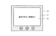
ところで、前記した表示装置によって表示される映像画面には、動画表示領域と非動画(静止画)表示領域が共存する場合がある。図1および図2はその一例を示したものであり、符号Aで示す全体の領域は表示装置によって表示される映像の全体画面を示しており、符号Bで示す領域は動画表示領域を示している。 By the way, a moving image display area and a non-moving image (still image) display area may coexist on the video screen displayed by the display device. FIG. 1 and FIG. 2 show an example thereof. The entire area indicated by reference numeral A indicates the entire screen of the video displayed by the display device, and the area indicated by reference numeral B indicates the moving image display area. Yes.
すなわち、図1および図2に示した例においては、動画表示領域Bの外側にCとして示した非動画表示領域が額縁状に形成され、前記額縁状の非動画表示領域Cの下側の領域には、例えばアイコンなどの固定パターンが表示された例を示している。 That is, in the example shown in FIG. 1 and FIG. 2, a non-moving image display area indicated as C is formed outside the moving image display area B in a frame shape, and the area below the frame-shaped non-moving image display area C Shows an example in which a fixed pattern such as an icon is displayed.
前記図1および図2に示したようにレイアウトされた表示画面Aにおいて、前記したPLE制御を行った場合には、このPLE制御はフィールドもしくはフレーム画面全体に対応する平均輝度レベル(APL)に基づいて、全体画面の表示輝度レベルを制御するように動作するので、例えば図1に示したように動画表示領域Bの画面が全体に明るい場合には、全体画面の表示輝度レベルが下げられて、Cとして示す非動画表示領域は暗く表示されるように制御される。 When the above-described PLE control is performed on the display screen A laid out as shown in FIGS. 1 and 2, the PLE control is based on the average luminance level (APL) corresponding to the entire field or frame screen. Therefore, when the screen of the moving image display area B is bright as a whole as shown in FIG. 1, for example, the display brightness level of the entire screen is lowered. The non-moving image display area indicated by C is controlled to be displayed darkly.
また、図2に示したように動画表示領域Bの画面が全体に暗い場合には、全体画面の表示輝度レベルが上げられて、Cとして示す非動画表示領域は明るく表示されるように制御される。すなわち、非動画表示領域Cは、動画表示領域Bの輝度レベルに応じて、その都度表示輝度レベルが制御されるために、ユーザに対しては非動画表示領域において、ちらつきが発生しているような見苦しさを感じさせる結果を招来させる。 Also, as shown in FIG. 2, when the screen of the moving image display area B is entirely dark, the display brightness level of the entire screen is increased, and the non-moving image display area indicated by C is controlled to be displayed brightly. The That is, since the display luminance level of the non-moving image display area C is controlled each time according to the luminance level of the moving image display area B, flickering appears in the non-moving image display area for the user. It brings about results that make you feel unsightly.
この発明は、動画表示領域と非動画表示領域が存在する画像を表示する表示手段において、PLE制御を実行するように構成した場合に発生する前記した技術的な問題点を解消できるようにした映像信号の表示制御装置および表示制御方法を提供することを課題とするものである。 According to the present invention, in the display means for displaying an image having a moving image display area and a non-moving image display area, an image capable of solving the above-described technical problems that occur when PLE control is executed is provided. It is an object of the present invention to provide a signal display control device and a display control method.
前記した課題を解決するためになされたこの発明にかかる表示制御装置における好ましい第1の基本形態は、請求項1に記載のとおり、複数のデータ線と複数の走査線の各交差位置に画素が配置され、入力映像信号に基づいて前記画素を選択的に点灯駆動させることで画像を表示する映像信号の表示制御装置であって、表示される前記画像内の非動画表示領域を検知することによって、表示される前記画像内の前記非動画表示領域以外の領域を動画表示領域として設定する動画表示領域設定手段と、前記動画表示領域設定手段により設定された動画表示領域における点灯する画素の割合である点灯率を算出する点灯率算出手段と、前記動画表示領域における点灯率に応じて、前記動画表示領域における発光輝度を可変制御する輝度制御手段を具備し、前記輝度制御手段は、前記点灯率算出手段により算出された前記動画表示領域における点灯率が大きくなる場合には、前記動画表示領域の発光輝度を下げ、前記点灯率が小さくなる場合には、前記動画表示領域の発光輝度を上げるように、発光輝度の可変制御を行い、前記非動画表示領域に対しては点灯率に応じた前記可変制御を行わないように構成される。
また、前記した課題を解決するためになされたこの発明にかかる表示制御装置における好ましい第2の基本形態は、請求項2に記載のとおり、複数のデータ線と複数の走査線の各交差位置に画素が配置され、入力映像信号に基づいて前記画素を選択的に点灯駆動させることで画像を表示する映像信号の表示制御装置であって、予め定められた前記各画素に対応する表示領域を指定することにより、もしくは前記各画素に対応する入力映像信号の時間変化を検出することにより、表示される前記画像内の動画表示領域を設定する動画表示領域設定手段と、前記動画表示領域設定手段により設定された動画表示領域における点灯する画素の割合である点灯率を算出する点灯率算出手段と、前記動画表示領域における点灯率に応じて、前記動画表示領域における発光輝度を可変制御する輝度制御手段を具備し、前記輝度制御手段は、前記点灯率算出手段により算出された前記動画表示領域における点灯率が大きくなる場合には、前記動画表示領域の発光輝度を下げ、前記点灯率が小さくなる場合には、前記動画表示領域の発光輝度を上げるように、発光輝度の可変制御を行い、表示される前記画像内の前記動画表示領域以外の非動画表示領域に対しては点灯率に応じた前記可変制御を行わないように構成される。
The first basic mode of the display control apparatus according to the present invention, which has been made to solve the above-described problems, is that, as described in
A second preferred basic form of the display control apparatus according to the present invention, which has been made to solve the above-mentioned problems, is as described in
また、前記した課題を解決するためになされたこの発明にかかる表示制御方法における好ましい第1の基本態様は、請求項12に記載のとおり、複数のデータ線と複数の走査線の各交差位置に画素が配置され、入力映像信号に基づいて前記画素を選択的に点灯駆動させることで画像を表示する映像信号の表示制御方法であって、複数のデータ線と複数の走査線の各交差位置に画素が配置され、入力映像信号に基づいて前記画素を選択的に点灯駆動させることで画像を表示する映像信号の表示制御方法であって、表示される前記画像内の非動画表示領域を検知することによって、表示される前記画像内の前記非動画表示領域以外の領域を動画表示領域として設定する動画表示領域設定動作と、前記動画表示領域設定動作により設定された動画表示領域における点灯する画素の割合である点灯率を算出する点灯率算出動作と、前記動画表示領域における点灯率が大きくなる場合には、前記動画表示領域の発光輝度を下げ、前記点灯率が小さくなる場合には、前記動画表示領域の発光輝度を上げるように、発光輝度の可変制御を行う輝度制御動作と、が実行され、前記輝度制御動作においては、非動画表示領域に対しては点灯率に応じた前記可変制御を行わないようになされる点に特徴を有する。
さらに、前記した課題を解決するためになされたこの発明にかかる表示制御方法における好ましい第2の基本態様は、請求項13に記載のとおり、複数のデータ線と複数の走査線の各交差位置に画素が配置され、入力映像信号に基づいて前記画素を選択的に点灯駆動させることで画像を表示する映像信号の表示制御方法であって、予め定められた前記各画素に対応する表示領域を指定することにより、もしくは前記各画素に対応する入力映像信号の時間変化を検出することにより、表示される前記画像内の動画表示領域を設定する動画表示領域設定動作と、前記動画表示領域設定動作により設定された動画表示領域における点灯する画素の割合である点灯率を算出する点灯率算出動作と、前記動画表示領域における点灯率が大きくなる場合には、前記動画表示領域の発光輝度を下げ、前記点灯率が小さくなる場合には、前記動画表示領域の発光輝度を上げるように、発光輝度の可変制御を行う輝度制御動作と、が実行され、前記輝度制御動作においては、表示される前記画像内の前記動画表示領域以外の非動画表示領域に対しては点灯率に応じた前記可変制御を行わないようになされる点に特徴を有する。
In addition, a preferable first basic aspect of the display control method according to the present invention, which has been made to solve the above-described problems, is as described in
Furthermore, a second preferred basic aspect of the display control method according to the present invention, which has been made to solve the above-mentioned problems, is as set forth in
以下、この発明にかかる映像信号の表示制御装置および表示制御方法について、図に示す実施の形態に基づいて説明する。なお、以下においては有機EL(エレクトロルミネッセンス)素子に代表される発光素子を表示画素として用いた表示パネルを点灯制御する例に基づいて説明する。 A video signal display control apparatus and display control method according to the present invention will be described below based on the embodiments shown in the drawings. The following description is based on an example in which lighting control is performed on a display panel using a light emitting element typified by an organic EL (electroluminescence) element as a display pixel.
図3は、その第1の形態を示したものであり、これはアクティブマトリクス型表示パネルを対象とした表示制御装置の例を示している。 FIG. 3 shows the first embodiment, which shows an example of a display control device intended for an active matrix display panel .
図3に示すようにコントローラ回路1にはアナログ/デジタル(A/D)変換部2および映像信号メモリ(以下、VRAMとも言う。)3が接続されており、アナログ映像信号による入力映像信号は、コントローラ回路1およびA/D変換部2に供給されるように構成されている。
As shown in FIG. 3, an analog / digital (A / D)
前記コントローラ回路1はアナログ映像信号中における水平および垂直同期信号に基づいて、前記A/D変換部2に対するクロック信号CK、前記VRAM3に対する書き込み信号Wおよび読み出し信号Rを生成する。
The
前記A/D変換部2は、コントローラ回路1から供給されるクロック信号CKに基づいて、入力されるアナログ映像信号をサンプリングし、これを1画素ごとの映像データに変換してVRAM3に供給するように作用する。前記VRAM3は前記コントローラ回路1からの書き込み信号WによってA/D変換部2から供給される映像データをVRAM3に順次書き込むように動作する。
The A /
前記VRAM3としては例えばフレームメモリが用いられており、前記した書き込み動作によって、後述する表示パネルにおける一画面分の映像信号の書き込みが行われる。また、VRAM3に書き込まれた映像信号は前記コントローラ回路1からの読み出し信号Rを受けて読み出され、動画表示領域設定手段4および輝度制御手段6に供給されるように構成されている。なお、図3においては、動画表示領域設定手段は、動画領域設定手段4と表記している。
For example, a frame memory is used as the
前記動画表示領域設定手段4としては、後述する表示パネルにおける画像の表示形態によって、二つの異なった機能を備えた構成を適宜採用することができる。その一つは、例えば図1および図2に示したように表示画面Aにおける動画表示領域Bと非動画表示領域Cとが常に定められて、各領域が変化しない場合である。この場合においては前記動画表示領域設定手段4としては、予め定められた動画表示領域を前記各画素単位で指定するように構成される。すなわち、動画表示領域設定手段4は予め定められた動画表示領域Bに対応するVRAM3からの映像データを抽出して、後述する点灯率算出手段5に供給するように動作する。
As the moving image display area setting means 4, a configuration having two different functions can be appropriately employed depending on an image display form on a display panel described later. For example, as shown in FIGS. 1 and 2, for example, a moving image display area B and a non-moving image display area C on the display screen A are always defined, and each area does not change. In this case, the moving image display area setting means 4 is configured to designate a predetermined moving image display area for each pixel. That is, the moving image display
また他の一つは、図1および図2に示した表示画面Aにおいて、動画表示領域Bと非動画表示領域Cとが入力映像信号によって変化する場合である。この場合においては、前記動画表示領域設定手段4としては、前記各画素に対応する入力映像信号の時間変化を検出することにより前記動画表示領域を検知し、その都度、動画表示領域を前記各画素単位で指定するように構成される。すなわち、この場合の動画表示領域設定手段4は、入力映像信号の時間変化の検出により設定される動画表示領域Bに対応するVRAM3からの映像信号を抽出して、後述する点灯率算出手段5に供給するように動作する。
The other is a case where the moving image display area B and the non-moving image display area C are changed by the input video signal on the display screen A shown in FIGS. 1 and 2. In this case, the moving image display area setting means 4 detects the moving image display area by detecting a time change of the input video signal corresponding to each pixel, and each time the moving image display area is set to each pixel. Configured to specify in units. That is, the moving image display area setting means 4 in this case extracts the video signal from the
なお、前記動画表示領域設定手段4は、前記した後者の場合において、非動画表示領域(静止画領域)を検知することによって、前記静止画領域以外の領域すなわち動画表示領域を設定するようにしてもよい。 In the latter case, the moving image display area setting means 4 detects a non-moving image display area (still image area) to set an area other than the still image area, that is, a moving image display area. Also good.
前記動画表示領域設定手段4からの動画表示領域に対応するVRAM3からの映像信号は点灯率算出手段5に供給され、この点灯率算出手段5は動画表示領域に対応する映像信号に基づいて画素単位の点灯率を算出するように動作する。なお、前記点灯率算出手段5は、動画表示領域に対応するすでに説明した映像信号の平均輝度レベル(APL)を算出する機能と同等の結果を得ることができる。
The video signal from the
前記点灯率算出手段5によって得られる動画表示領域における点灯率のデータは、輝度制御手段6に供給される。この輝度制御手段6には前記したとおりVRAM3から読み出された映像データが供給されるように構成されており、前記輝度制御手段6はVRAM3から読み出された映像信号のうち、動画表示に対応する映像信号の階調値を前記点灯率に基づいて変更する映像信号の変換処理を実行する。
The data of the lighting rate in the moving image display area obtained by the lighting
すなわち、輝度制御手段6はVRAM3から読み出された映像信号のうち、動画表示に寄与する映像信号を前記点灯率算出手段5により算出された画素の点灯率に応じた輝度に対応する階調値に変換する処理を実行するように動作する。これにより、後述する表示パネルに配列された動画表示領域における各画素の発光輝度を制御するPLE制御が実現される。そして、輝度制御手段6はPLE制御による階調制御が施された前記映像信号を、後述するデータドライバにおいて駆動可能な信号形態に変換して出力する。
That is, the
なお、前記したコントローラ回路1は、映像信号中における前記水平および垂直同期信号に基づいて、後述する走査ドライバ13およびデータドライバ14に対するシフトクロック信号やスタートパルス等を生成し、それぞれのドライバ13,14に供給するように構成されている。
The
図3に示す符号11は前記した有機EL素子からなる発光素子をそれぞれに含む多数の画素12をマトリクス状に配列した表示パネルを示している。この表示パネル11には、走査ドライバ13、データドライバ14にそれぞれ接続される走査線21、データ線22が互いに直交する方向に配列されており、これらの交差位置に前記発光素子を含む画素12がそれぞれ配置されている。なお、前記各画素12には、電源供給回路16より画素の点灯駆動用電圧が電源供給線24を介して、それぞれ供給されるように構成されている。
図4は前記した表示パネル11に配置された1つの画素に対応する回路構成を示すものであり、これは発光素子として有機EL素子を用いる場合の最も基本的な画素構成を示している。この画素12には前記データドライバ14からの映像信号に対応したデータ信号Vdataが、表示パネルに配列されたデータ線22を介して制御用TFT、すなわちデータ書き込みトランジスタTr1のソースに供給されるように構成されている。
FIG. 4 shows a circuit configuration corresponding to one pixel arranged on the
前記データ書き込みトランジスタTr1のゲートには、走査ドライバ13に接続された走査線21を介して走査信号Select(これを書き込みパルスとも言う。)が供給されるように構成されている。前記データ書き込みトランジスタTr1のドレインは、点灯駆動用TFT、すなわち点灯駆動トランジスタTr2のゲートに接続されると共に、電荷保持用キャパシタC1の一方の端子に接続されている。
A scanning signal Select (also referred to as a writing pulse) is supplied to the gate of the data writing transistor Tr1 through a
また、点灯駆動トランジスタTr2のソースは、前記キャパシタC1の他方の端子に接続されると共に、電源供給線24を介して前記した電源供給回路16より駆動電圧Vccが供給されるように構成されている。前記点灯駆動トランジスタTr2のドレインは、発光素子としての有機EL素子E1のアノード端子に接続され、この有機EL素子E1のカソード端子は、表示パネルの基準電位点(グランド)に接続されている。
Further, the source of the lighting drive transistor Tr2 is connected to the other terminal of the capacitor C1, and the drive voltage Vcc is supplied from the
なお、図4に示す画素12の回路構成においては、データ書き込みトランジスタTr1がnチャンネル型TFTにより構成され、駆動トランジスタTr2がpチャンネル型TFTにより構成されている。そして、前記した構成による画素12は、図3に示したように行および列方向にマトリクス状に多数配置されて表示パネル11が構成されている。
In the circuit configuration of the
図4に示した画素12の構成において、制御トランジスタTr1のゲートには、アドレス期間において走査ドライバ13より走査信号としての書き込みパルスSelectが供給される。この時、データドライバ14から供給されるデータ信号Vdataが画素を点灯させるデータである場合においては、制御トランジスタTr1のソース・ドレインを介して、データ信号Vdataに対応した電流がキャパシタC1に流れ、キャパシタC1は充電される。
In the configuration of the
そして、その充電電圧が駆動トランジスタTr2のゲートに供給されて、トランジスタTr2はそのゲート電圧とドレインに供給される駆動電圧Vccに対応した電流を前記EL素子E1に流し、これによりEL素子E1は発光(点灯)する。 Then, the charging voltage is supplied to the gate of the driving transistor Tr2, and the transistor Tr2 supplies a current corresponding to the gate voltage and the driving voltage Vcc supplied to the drain to the EL element E1, whereby the EL element E1 emits light. (Light.
前記制御トランジスタTr1のゲートに対する前記書き込みパルスの印加が停止されると、トランジスタTr1はいわゆるカットオフとなる。しかしながら、キャパシタC1に蓄積された電荷により駆動トランジスタTr2のゲート電圧が保持され、これによりEL素子E1への駆動電流が維持される。 When application of the write pulse to the gate of the control transistor Tr1 is stopped, the transistor Tr1 becomes a so-called cutoff. However, the gate voltage of the drive transistor Tr2 is held by the electric charge accumulated in the capacitor C1, thereby maintaining the drive current to the EL element E1.
したがって、EL素子E1は次のアドレス動作に至る期間において、前記データ信号Vdataに対応した点灯状態を継続することができる。それ故、前記したアドレス期間において、データドライバ14から供給されるデータ信号Vdataに応じて画素の点灯もしくは消灯が制御され、これにより各画素の単位期間における点灯期間が個別に制御されて階調制御が実現される。
Therefore, the EL element E1 can continue the lighting state corresponding to the data signal Vdata during the period until the next address operation. Therefore, in the address period described above, the lighting or extinguishing of the pixels is controlled in accordance with the data signal Vdata supplied from the
図3および図4に示した実施の形態においては、前記したPLE制御による階調表現を実現させるために、1フレーム期間を複数のサブフレームに分割し、各サブフレームごとに画素の点灯または非点灯を制御することで、1フレーム期間内における画素の点灯期間の累計により階調制御を実現する制御手段が採用されている。 In the embodiment shown in FIGS. 3 and 4, one frame period is divided into a plurality of subframes in order to realize the gradation expression by the PLE control, and the pixel is turned on or off for each subframe. By controlling lighting, a control means is employed that realizes gradation control based on the total number of lighting periods of pixels within one frame period.
図5はその階調制御の一例を示すものであり、この例においては説明を簡素化するために1フレーム期間を7つのサブフレームに分割し、サブフレーム期間の単純な累計により“階調0”〜“階調7”の8階調を表現する単純サブフレーム法を示している。この例においてはサブフレーム期間ごとに、そのサブフレーム期間の開始時に、前記したデータドライバ14より画素を点灯または非点灯に制御するデータ信号Vdataが供給される。
FIG. 5 shows an example of the gradation control. In this example, in order to simplify the explanation, one frame period is divided into seven subframes, and “
ここで1つのフレーム期間を構成する第1〜第7のサブフレームの全てにおいて、画素を非点灯に制御するデータ信号が供給された場合には、図5に示すように“階調0”が実現される。また、第1〜第7のサブフレームの全てにおいて、画素を点灯状態に制御するデータ信号が供給された場合には、図5に示すように“階調7”が実現される。
Here, in all of the first to seventh sub-frames constituting one frame period, when a data signal for controlling the pixel to be non-lighted is supplied, as shown in FIG. Realized. Further, in all of the first to seventh subframes, when a data signal for controlling the pixel to be in a lighting state is supplied, “
前記した輝度制御手段6はすでに説明したとおり、動画表示領域に対応する画素の点灯率に応じて、動画表示領域の画素の階調を制御するものであり、点灯率が大きくなる場合には階調を低くする制御を実行するように動作する。これにより、動画表示領域に対応する画素の点灯率が例えば100%に近い状態である場合においては、入力される映像信号に基づく階調に対して、階調がn段(nは整数)下げるように動作する。したがって、前記点灯率が高い場合においては、動画表示領域における画素の1フレーム期間における点灯期間は縮小され、当該画素の発光輝度は抑制される。この結果、低消費電力化を実現させることができる。 As described above, the luminance control means 6 controls the gradation of the pixels in the moving image display area in accordance with the lighting rate of the pixels corresponding to the moving image display area. It operates to execute control to lower the key. Thereby, when the lighting rate of the pixel corresponding to the moving image display area is in a state close to 100%, for example, the gradation is lowered by n stages (n is an integer) with respect to the gradation based on the input video signal. To work. Therefore, when the lighting rate is high, the lighting period in one frame period of the pixel in the moving image display area is reduced, and the light emission luminance of the pixel is suppressed. As a result, low power consumption can be realized.
一方、動画表示領域に対応する画素の点灯率が小さくなる場合には、入力される映像信号に基づく階調に対して、動画表示領域の階調をn段(nは整数)上げるように動作する。これにより、動画表示領域における画素の1フレーム期間における累積点灯期間が拡大され、動画表示領域におけるコントラストの良好な画像を表示させることが可能となる。なお、前記した実施の形態によると、非動画(静止画)領域においてはPLE動作は実行されないので、非動画領域の階調は入力映像信号に基づく階調で表示される。 On the other hand, when the lighting rate of the pixel corresponding to the moving image display area is small, the gradation of the moving image display area is increased by n stages (n is an integer) with respect to the gradation based on the input video signal. To do. Thereby, the cumulative lighting period in one frame period of the pixels in the moving image display area is expanded, and an image with good contrast in the moving image display area can be displayed. According to the embodiment described above, since the PLE operation is not executed in the non-moving image (still image) region, the gradation of the non-moving image region is displayed with a gradation based on the input video signal.
次に、前記した図3および図4に示した表示制御装置の構成を利用して、他のPLE制御動作を実現させることもできる。 Next, other PLE control operations can be realized using the configuration of the display control apparatus shown in FIGS .
この実施の形態における前記輝度制御手段6は、動画表示領域に対応する各データ線に供給するデータドライバ14からの出力電圧値を、点灯率算出手段5により得られる動画表示領域における画素の点灯率に応じて可変制御するように構成した点に特徴を有する。
In this embodiment, the luminance control means 6 uses the output voltage value from the
この場合における図4に示す画素構成におけるデータ書き込みトランジスタTr1および点灯駆動トランジスタTr2はアナログ動作(定電流駆動)領域にて動作するように設定される。そして、各走査線21に対応するそれぞれのアドレス期間において、動画表示領域に対応する各データ線に供給するデータドライバ14からのデータ信号Vdataの電圧値が、前記点灯率算出手段5により得られる点灯率に応じて可変制御されるように構成される。
In this case, the data writing transistor Tr1 and the lighting drive transistor Tr2 in the pixel configuration shown in FIG. 4 are set to operate in the analog operation (constant current drive) region. Then, in each address period corresponding to each
この結果、各走査線21に対応するそれぞれのアドレス期間において、各画素の電荷保持用キャパシタC1に書き込まれる電圧値は、前記データ信号Vdataの電圧値に対応したものとなる。そして、点灯駆動トランジスタTr2は電荷保持用キャパシタC1に書き込まれた電圧値に対応した駆動電流を、前記EL素子E1に供給するように動作する。したがって、動画表示領域に対応する各画素12の輝度は、前記した点灯率算出手段5により得られる点灯率に応じて可変制御されるPLE動作が実現される。
As a result, in each address period corresponding to each
この場合、各走査線21に対応するそれぞれのアドレス期間において、非動画表示領域に対応する各データ線に供給されるデータドライバ14からのデータ信号Vdataの電圧値は、前記点灯率に関係なく入力映像信号に基づいて制御される。したがって、非動画領域における画素の発光輝度が、前記点灯率による影響を受ける問題を回避することができる。
In this case, in each address period corresponding to each
図6は、この発明にかかる他の表示制御装置の例を示すものである。なお、図6に示す構成において、すでに説明した図3に示す各部と同様の機能を果たす部分を同一符号で示しており、したがってその詳細な説明は省略する。また、図6に示す表示制御装置の構成においても、表示パネル11に配列された各画素12の構成は、図4に示した構成を採用することができる。
6, Ru der shows an example of such other display control device according to the present invention. In the configuration shown in FIG. 6, parts that perform the same functions as the parts shown in FIG. 3 already described are denoted by the same reference numerals, and thus detailed description thereof is omitted. Also in the configuration of the display control device shown in FIG. 6, the configuration shown in FIG. 4 can be adopted as the configuration of each
この図6に示す実施の形態における輝度制御手段6は、動画表示領域に対応する画素に接続された電源供給線24に対して、点灯率算出手段5により得られる動画表示領域における画素の点灯率に応じて可変される駆動電圧を供給し、非動画表示領域に対応する画素に接続された電源供給線24に対しては、予め定められた値の駆動電圧を供給するように構成した点に特徴を有する。
The luminance control means 6 in the embodiment shown in FIG. 6 has the pixel lighting rate in the moving image display area obtained by the lighting rate calculation means 5 for the
このために前記電源供給回路16には、輝度制御手段6からの輝度制御(PLE制御)データによって出力値が可変される可変電圧源EV1と、予め定められた値の電圧が出力される固定電圧源EF1が備えられている。そして、前記可変電圧源EV1もしくは固定電圧源EF1からの駆動電圧を、各電源供給線24に対して選択的に供給するための選択手段としてのスイッチS1,S2,……が各電源供給線24に対応して備えられている。
For this purpose, the
また、図6に示すように動画表示領域設定手段4により設定される動画表示領域の情報データが、コントローラ回路1に供給されるように構成されている。そして、前記コントローラ回路1は前記動画表示領域の情報データを受けて、電源供給回路16における前記各スイッチS1,S2,……を、前記可変電圧源EV1もしくは固定電圧源EF1側に択一的に接続するように制御する。
Further, as shown in FIG. 6, the moving image display area information data set by the moving image display
すなわち、前記動画表示領域設定手段4からの動画表示領域の情報に基づいて、動画表示領域の画素に対応する電源供給線24には、前記各スイッチS1,S2,……を介して可変電圧源EV1からの駆動電圧が供給されるように動作し、非動画表示領域の画素に対応する電源供給線24には、前記各スイッチS1,S2,……を介して固定電圧源EF1からの駆動電圧が供給されるように動作する。
That is, based on the information on the moving image display area from the moving image display area setting means 4, the
したがって、動画表示領域の各画素12には、輝度制御手段6からの輝度制御データによって出力値が可変される可変電圧源EV1からの駆動電圧が供給され、これにより、動画表示領域に対応する各画素12の輝度は、前記した点灯率算出手段5により得られる点灯率に応じて可変制御されるPLE動作が実現される。一方、非動画表示領域の各画素12には、固定電圧源EF1からの駆動電圧が供給されるので、非動画表示領域に対応する各画素12は一定の輝度に保つことができる。
Therefore, each
なお、図6に示した実施の形態によると、表示パネル11における電源供給線24の配列方向によって、動画表示領域および非動画表示領域が区画されることになる。すなわち、図6に示した表示パネル11のように電源供給線24の配列方向が縦方向である場合には、図7に示したように画面Aにおいて、動画表示領域Bおよび非動画表示領域Cが縦方向の線で区画されることになる。
According to the embodiment shown in FIG. 6, the moving image display area and the non-moving image display area are divided according to the arrangement direction of the
したがって、図6に示す走査線21、データ線22、電源供給線24の配列関係を、表示パネル11上においてそのまま例えば90度回転させた状態に配列することで、図8に示すように画面Aにおいて、動画表示領域Bおよび非動画表示領域Cが横方向の線で区画されるように構成させることができる。
Therefore, by arranging the arrangement relationship of the
図9は、この発明にかかる他の表示制御装置の例を示すものであり、これはパッシブマトリクス型表示パネルを対象とした表示制御装置の例を示している。 FIG. 9 shows an example of another display control device according to the present invention, which shows an example of a display control device intended for a passive matrix display panel .
この図9に示す表示制御装置の構成においても、すでに説明した図6に示した構成と同様にコントローラ回路1、A/D変換部2、VRAM3、動画表示領域設定手段4、点灯率算出手段5、輝度制御手段6が具備されるが、図9においてはコントローラ回路1、輝度制御手段6を除き、前記他の構成は省略して示している。
Also in the configuration of the display control apparatus shown in FIG. 9, the
この図9に示す実施の形態における輝度制御手段6は、動画表示領域に対応する画素に接続されたデータ線に対して、点灯率算出手段5により得られる動画表示領域における画素の点灯率に応じて可変される駆動電流を供給し、非動画表示領域に対応する画素に接続されたデータ線に対しては、予め定められた値の駆動電流を供給するように構成した点に特徴を有する。 The luminance control means 6 in the embodiment shown in FIG. 9 responds to the lighting rate of the pixels in the moving image display area obtained by the lighting rate calculation means 5 for the data lines connected to the pixels corresponding to the moving image display area. It is characterized in that a driving current having a predetermined value is supplied to a data line connected to a pixel corresponding to a non-moving picture display region.
図9に示す表示パネル31には、n本のデータ線としての陽極線A1〜Anが縦方向(列方向)に配列され、m本の走査線としての陰極線K1〜Kmが横方向(行方向)に配列され、各々の交差した部分(計n×m箇所)に、ダイオードのシンボルマークで示した画素を構成する有機EL素子E11〜Enmが各陽極線と走査線との間に接続されて配置されている。そして、各陽極線A1〜Anはデータドライバとしての陽極線ドライブ回路32に接続され、各陰極線K1〜Kmは同じく走査ドライバとしての陰極線走査回路33に接続されてそれぞれ駆動される。
In the
前記陽極線ドライブ回路32には、駆動電圧VHを利用して動作する第1群の定電流源Ia1〜Ianが備えられている。この第1群の定電流源Ia1〜Ianには、前記輝度制御手段6からのPLE制御に基づく信号が供給される。これにより第1群の定電流源Ia1〜Ianは、すでに説明した点灯率算出手段5により得られる動画表示領域における画素の点灯率に応じて、その出力電流値(駆動電流値)が制御されるように動作する。
The anode
一方、陽極線ドライブ回路32には、第2群の定電流源Ib1〜Ibnが備えられており、これは予め定められた値の駆動電流を供給するように構成されている。そして、前記第1群または第2群の定電流源、もしくは基準電位点としてのグランドを選択することができる選択手段としてのドライブスイッチSa1〜Sanが各陽極線A1〜Anに対応して備えられており、このドライブスイッチSa1〜Sanは、コントローラ回路1からの指令信号によって切り換えられるように構成されている。
On the other hand, the anode
また、前記陰極線走査回路33には、各陰極線K1〜Kmに対応して走査スイッチSk1〜Skmが備えられ、コントローラ回路1からの指令信号によって、非走査選択電位として機能するクロストーク発光を防止するための逆バイアス電圧源VMまたは走査選択電位として機能するグランド電位のうちのいずれか一方を、対応する陰極線に接続するように作用する。
The cathode
これにより、陰極線を所定の周期で基準電位点(グランド電位)に設定しながら、所望の陽極線A1〜Anに第1群または第2群の定電流源を接続することにより、前記各EL素子を選択的に発光させるように作用する。 Accordingly, each of the EL elements can be obtained by connecting the first group or the second group of constant current sources to desired anode lines A1 to An while setting the cathode line to a reference potential point (ground potential) at a predetermined cycle. Acts to selectively emit light.
なお、図9に示す実施の形態においては、コントローラ回路1より陰極線走査回路33に対して走査同期信号が供給され、これにより各陰極線K1〜Kmを順次グランド電位(走査選択電位)に設定する動作が繰り返される。またコントローラ回路1より陽極線ドライブ回路32に対して走査同期信号に同期して走査ラインごとにドライブ制御信号が供給される。
In the embodiment shown in FIG. 9, a scanning synchronization signal is supplied from the
すなわち、コントローラ回路1には、図6に基づいてすでに説明したように動画表示領域設定手段4により設定される動画表示領域の情報データが供給される。コントローラ回路1は、これに基づいて動画表示領域の画素を点灯させる場合においては第1群の定電流源Ia1〜Ianを選択するようにドライブスイッチSa1〜Sanを制御し、非動画表示領域の画素を点灯させる場合においては第2群の定電流源Ib1〜Ibnを選択するようにドライブスイッチSa1〜Sanを制御する。さらに画素を非点灯にする場合には基準電位(グランド電位)を選択するようにドライブスイッチSa1〜Sanを制御する。
That is, the
したがって、動画表示領域の各画素(EL素子)には、輝度制御手段6からの輝度制御(PLE制御)データによって定電流値が可変される第1群の定電流源Ia1〜Ianからの駆動電流が供給される。これにより、動画表示領域に対応する各画素の輝度は、すでに説明した点灯率算出手段5により得られる点灯率に応じて可変制御されるPLE動作が実現される。一方、非動画表示領域の各画素には、第1群の定電流源Ia1〜Ianからの一定の駆動電流が供給されるので、非動画表示領域に対応する各画素の輝度を一定の輝度に保つことができる。 Therefore, the driving current from the first group of constant current sources Ia1 to Ian whose constant current value is varied by the luminance control (PLE control) data from the luminance control means 6 is applied to each pixel (EL element) in the moving image display area. Is supplied. Thereby, the PLE operation is realized in which the luminance of each pixel corresponding to the moving image display area is variably controlled according to the lighting rate obtained by the lighting rate calculation means 5 described above. On the other hand, each pixel in the non-moving picture display area is supplied with a constant driving current from the first group of constant current sources Ia1 to Ian, so that the brightness of each pixel corresponding to the non-moving picture display area is made constant. Can keep.
なお、図9に示した実施の形態においても、表示パネル31におけるデータ線としての陽極線A1〜Anの配列方向によって、動画表示領域および非動画表示領域が区画されることになる。すなわち、図9に示した表示パネル31のように陽極線A1〜Anの配列方向が縦方向である場合には、図7に示したように画面Aにおいて、動画表示領域Bおよび非動画表示領域Cが縦方向の線で区画されることになる。
In the embodiment shown in FIG. 9 as well, the moving image display region and the non-moving image display region are divided according to the arrangement direction of the anode lines A1 to An as the data lines in the
したがって、図9に示す直交関係にあるデータ線A1〜An、走査線K1〜Kmの配列関係を、表示パネル31上においてそのまま例えば90度回転させた状態に配列することで、図8に示すように画面Aにおいて、動画表示領域Bおよび非動画表示領域Cが横方向の線で区画されるように構成せることができる。
Therefore, by arranging the arrangement relationship of the data lines A1 to An and the scanning lines K1 to Km in the orthogonal relationship shown in FIG. 9 as it is, for example, rotated by 90 degrees on the
図10〜図13は、この発明にかかるさらに他の表示制御装置の例を示すものであり、これはSES(Simultaneous Erasing Scan)駆動方式を採用したアクティブマトリクス型表示パネルを対象とした表示制御装置の例を示している。 10 to 13 show another example of the display control device according to the present invention, which is a display control device for an active matrix display panel adopting a SES (Simultaneous Erasing Scan) driving method. An example is shown.
なお、図10に示す構成においては、すでに説明した図6に示す各部と同様の機能を果たす部分を同一符号で示しており、したがってその詳細な説明は省略する。 In the configuration shown in FIG. 10, portions that perform the same functions as those shown in FIG. 6 already described are denoted by the same reference numerals, and thus detailed description thereof is omitted.
この図10〜図13に示す実施の形態においては、動画表示領域に対応する点灯対象にされる画素を、1フレームもしくは1サブフレーム期間の途中において非点灯(消灯)状態に制御する消灯走査手段が具備される。そして、輝度制御手段6は前記消灯走査手段における消灯動作のタイミングを、点灯率算出手段5により得られる動画表示領域における画素の点灯率に応じて制御するようにした点に特徴を有する。 In the embodiment shown in FIGS. 10 to 13, a light-off scanning unit that controls a pixel to be turned on corresponding to a moving image display area to a non-lighting (light-off) state during one frame or one subframe period. Is provided. The brightness control means 6 is characterized in that the timing of the turn-off operation in the turn-off scanning means is controlled in accordance with the lighting rate of the pixels in the moving image display area obtained by the lighting rate calculation means 5.
前記した動作を実現させるために図10に示した構成においては、すでに説明した図6に示す構成に対して消去タイミング信号生成手段8および前記した消灯走査手段として機能する消去ドライバ15が具備されている。前記消去タイミング信号生成手段8は、コントローラ回路1からの同期信号、および輝度制御手段6からの輝度制御(PLE制御)データによって、消去制御信号(消去パルス)の出力タイミングを調整するように動作するものである。なお、この消去タイミング信号生成手段8については、図13に基づいて後で詳しく説明する。
In order to realize the above-described operation, the configuration shown in FIG. 10 is provided with an erase timing signal generating means 8 and an erase
一方、前記消去ドライバ15は消去タイミング信号生成手段8からのタイミング信号を受けて、1フレームもしくは1サブフレーム期間の途中において、画素12を消灯動作させるように機能する。すなわち表示パネル11には、各画素12の走査線21に対応して消去信号線23が配列されており、この消去信号線23に消去パルスを供給することにより、当該消去信号線23に対応する画素を消灯させるように動作する。
On the other hand, the erase
図11は前記したSES駆動方式において好適に採用される画素の構成例を示したものである。この図11に示す画素の構成例は、図4に示した画素の構成に加えてTFTによる消去用トランジスタTr3がさらに具備されている。そして、消去用トランジスタTr3のソースおよびドレインは電荷保持用キャパシタC1の両端にそれぞれ接続されており、そのゲートには表示パネル11に配列された前記消去信号線23を介して消去ドライバ15より消去パルスEraseが供給されるように構成されている。
FIG. 11 shows a configuration example of a pixel that is preferably employed in the above-described SES driving method. The configuration example of the pixel shown in FIG. 11 further includes an erasing transistor Tr3 using a TFT in addition to the configuration of the pixel shown in FIG. The source and drain of the erasing transistor Tr3 are respectively connected to both ends of the charge holding capacitor C1, and the erasing pulse is supplied to the gate of the erasing transistor Tr3 from the erasing
前記した画素の構成において、トランジスタTr1およびTr2の働きは、図4に示した例と同様である。一方、消去トランジスタTr3のゲートには、前記EL素子E1の点灯期間の途中(この実施の形態においては、1サブフレーム期間の途中)のタイミングにおいて、前記消去ドライバ15よりトランジスタTr3をオンさせる消去パルスEraseが消去信号線23を介して供給される。
In the pixel configuration described above, the functions of the transistors Tr1 and Tr2 are the same as in the example shown in FIG. On the other hand, at the gate of the erasing transistor Tr3, an erasing pulse for turning on the transistor Tr3 by the erasing
これにより、キャパシタC1にチャージされている電荷は瞬時にして消去(放電)される。この結果、駆動トランジスタTr2はカットオフ状態となり、EL素子E1は直ちに消灯される。換言すれば、消去ドライバ15からの消去パルスEraseの出力タイミングを制御することで、EL素子E1の1サブフレームにおける点灯期間が制御され、これにより多階調表現を実現させることができる。
Thereby, the electric charge charged in the capacitor C1 is erased (discharged) instantaneously. As a result, the drive transistor Tr2 is cut off, and the EL element E1 is immediately turned off. In other words, by controlling the output timing of the erase pulse Erase from the erase
図12は、図10および図11に示した構成によってなされる動画表示領域のPLE制御を説明するものである。このPLE制御を実現させるにあたって、この実施の形態においては1フレーム期間を複数のサブフレームに分割し、このサブフレームの選択による1フレーム期間内における画素の点灯期間の累計により階調制御を実現する制御手段が採用されている。 FIG. 12 illustrates the PLE control of the moving image display area performed by the configuration shown in FIGS. 10 and 11. In realizing this PLE control, in this embodiment, one frame period is divided into a plurality of subframes, and gradation control is realized by the total number of lighting periods of pixels within one frame period by selecting this subframe. Control means are employed.
すなわち図12に示す例は、説明を簡素化するために1フレーム期間を7つのサブフレーム(SF1〜SF7)に分割し、1フレーム期間における各サブフレームを選択することで、8つの階調表現(100%非点灯も1つの階調と見なすことができ、7+1の階調表現)を実現する例を示している。 That is, in the example shown in FIG. 12, one frame period is divided into seven subframes (SF1 to SF7) to simplify the description, and each gray level is expressed by selecting each subframe in one frame period. In this example, 100% non-lighting can be regarded as one gradation, and 7 + 1 gradation expression is realized.
図12(a)および(b)は、前記輝度制御手段6からの輝度制御データに基づいて、サブフレームごとの点灯期間と非点灯期間の割合を制御する例を示したものであり、(a)はサブフレームごとの点灯期間の割合が大きく、また(b)はサブフレームごとの点灯期間の割合が小さい場合を示している。なお、前記(a)および(b)は共に階調特性のガンマ値が同一で、ディマー特性が変更される例を示している。 FIGS. 12A and 12B show an example of controlling the ratio of the lighting period and the non-lighting period for each subframe based on the luminance control data from the luminance control means 6. ) Shows a case where the ratio of the lighting period for each subframe is large, and (b) shows a case where the ratio of the lighting period for each subframe is small. Note that (a) and (b) show examples in which the gamma values of the gradation characteristics are the same and the dimmer characteristics are changed.
ここで、動画表示領域における画素の点灯率が低い場合においては、動画表示領域において図12(a)に示す点灯制御が実行され、動画表示領域における画素の点灯率が高い場合においては動画表示領域において図12(b)に示す点灯制御が実行されるように制御される。要するに画素の点灯率の程度に応じて、サブフレームごとの点灯期間の割合が図12(a)と(b)の間で変化するように制御される。これにより、特に画素の点灯率が高い場合においては1フレーム期間内における画素の点灯期間の累計が低く抑えられ、各画素に供給される駆動電流値を抑制させることができる。 Here, when the lighting rate of the pixel in the moving image display area is low, the lighting control shown in FIG. 12A is executed in the moving image display area, and when the lighting rate of the pixel in the moving image display area is high, the moving image display area In FIG. 12, the lighting control shown in FIG. 12B is executed. In short, the ratio of the lighting period for each subframe is controlled so as to change between FIGS. 12A and 12B in accordance with the degree of lighting rate of the pixels. Thereby, especially when the lighting rate of the pixel is high, the cumulative number of lighting periods of the pixel within one frame period can be suppressed low, and the drive current value supplied to each pixel can be suppressed.
図12(c)および(d)は、図12(b)に示した点灯制御を実現させる場合の前記した書き込みパルスおよび消去パルスの発生タイミングを説明するものである。すなわち、図12に示す例においては、各サブフレームのスタートに同期して(c)に示す書き込みパルスが発生し、これにより画素は点灯状態にされる。そして、そのサブフレームの経過途中において(d)として示す消去パルスが発生し、これにより画素は非点灯状態にされる。 FIGS. 12C and 12D are diagrams for explaining the generation timing of the write pulse and the erase pulse when the lighting control shown in FIG. 12B is realized. In other words, in the example shown in FIG. 12, the write pulse shown in (c) is generated in synchronization with the start of each subframe, whereby the pixel is turned on. Then, in the middle of the subframe, an erasing pulse shown as (d) is generated, whereby the pixel is turned off.
ここで、例えば“階調8”を実現しようとした場合には、1フレーム期間において、画素は図12(a)または(b)に示す一連の点灯パターンが実行される。また例えば“階調5”を実現しようとした場合には、図12(a)または(b)に示すSf1〜Sf4の期間において点灯駆動動作が実行され、それ以降の各サブフレームの期間Sf5〜Sf7は全て消灯状態にされる。これにより、1フレーム期間における画素の点灯期間の累計にしたがった発光輝度を得ることができる。
Here, for example, when “
図12(d)に示す消去パルスは、次に説明する図13に示す消去タイミング信号生成手段8によって生成することができる。図13における符号8aはサブフレームカウンタを、符号8bは論理演算ユニットを、さらに符号8cは輝度設定テーブルを示している。すなわち、サブフレームカウンタ8aはコントローラ1からの同期信号に基づいて、サブフレームに同期した制御信号を論理演算ユニット8bに供給するように動作する。
The erase pulse shown in FIG. 12D can be generated by the erase timing signal generating means 8 shown in FIG. In FIG. 13, reference numeral 8a denotes a subframe counter,
また、前記輝度設定テーブル8cには、前記輝度制御手段6からの輝度制御(PLE制御)データが供給され、この輝度制御データに基づいて適切な輝度設定テーブルが選択される。なお、選択された輝度設定テーブル8cには、各サブフレームごとの点灯期間がパラメータとして格納されている。 The luminance setting table 8c is supplied with luminance control (PLE control) data from the luminance control means 6, and an appropriate luminance setting table is selected based on the luminance control data. In the selected luminance setting table 8c, the lighting period for each subframe is stored as a parameter.
そして、サブフレームカウンタ8aより、点灯制御されるべきサブフレームナンバが論理演算ユニット8bに供給された場合、論理演算ユニット8bは選択されたテーブルをアクセスし、サブフレームナンバに対応して格納されている点灯時間のパラメータに基づいて、消去パルスの出力タイミング信号を生成するように動作する。
When the subframe number to be lit is supplied from the subframe counter 8a to the
これは図12(d)に示したように動画表示領域の画素の点灯率にそれぞれ対応してサブフレームごとの消去パルスの出力タイミング信号として生成される。このタイミング信号は前記した消去ドライバ15に供給され、消去ドライバ15からは前記したとおり、各サブフレームごとに消去パルスを出力するように動作する。
As shown in FIG. 12D, this is generated as an output timing signal of an erase pulse for each subframe corresponding to the lighting rate of the pixels in the moving image display area. This timing signal is supplied to the above-described erase
前記した実施の形態によると、特定のガンマ特性を持たせた状態で、動画表示領域の画素の点灯率に基づいてPLE制御を行うように動作する。なお、前記した消去ドライバ15は動画表示領域に対応して消去動作を実行し、これにより動画表示領域の輝度制御が実行される。換言すれば、非動画表示領域においては消去ドライバ15による消去動作は実行されず、非動画表示領域に対応する画素においては、入力映像信号に基づく階調になされる。
According to the above-described embodiment, the PLE control is performed based on the lighting rate of the pixels in the moving image display area with a specific gamma characteristic. The erasing
なお、図10〜図13に示した実施の形態においても、表示パネル11に配列された消去信号線23の配列方向によって、動画表示領域および非動画表示領域が区画されることになる。すなわち、図10に示した表示パネル11のように消去信号線23の配列方向が横方向である場合には、図8に示したように画面Aにおいて、動画表示領域Bおよび非動画表示領域Cは横方向の線で区画されることになる。
10 to 13, the moving image display area and the non-moving image display area are divided according to the arrangement direction of the erasing
したがって、図10に示す走査線21、データ線22、消去信号線23の配列関係を、表示パネル11上においてそのまま例えば90度回転させた状態に配列することで、図7に示すように画面Aにおいて、動画表示領域Bおよび非動画表示領域Cが縦方向の線で区画されるように構成させることができる。
Therefore, by arranging the arrangement relationship of the
1 コントローラ回路
2 A/D変換部
3 映像信号メモリ
4 動画表示領域設定手段
5 点灯率算出手段
6 輝度制御手段
8 消去タイミング信号生成手段
11,31 表示パネル
12 画素
13,33 走査ドライバ
13,32 データドライバ
15 消去ドライバ(消灯走査手段)
16 電源供給回路
21 走査線
22 データ線
23 消去信号線
24 電源供給線
A 映像画面
B 動画表示領域
C 非動画(静止画)表示領域
C1 電荷保持用キャパシタ
E1,E11〜Enm EL素子(発光素子)
EF1 固定電圧源
EV1 可変電圧源
Ia1〜Ian 定電流源(第1群)
Ib1〜Ibn 定電流源(第2群)
Tr1 データ書き込みトランジスタ
Tr2 点灯駆動トランジスタ
Tr3 消去用トランジスタ
DESCRIPTION OF
16
EF1 fixed voltage source EV1 variable voltage source Ia1 to Ian constant current source (first group)
Ib1 to Ibn constant current source (second group)
Tr1 data writing transistor Tr2 lighting drive transistor Tr3 erasing transistor
Claims (18)
表示される前記画像内の非動画表示領域を検知することによって、表示される前記画像内の前記非動画表示領域以外の領域を動画表示領域として設定する動画表示領域設定手段と、前記動画表示領域設定手段により設定された動画表示領域における点灯する画素の割合である点灯率を算出する点灯率算出手段と、前記動画表示領域における点灯率に応じて、前記動画表示領域における発光輝度を可変制御する輝度制御手段を具備し、
前記輝度制御手段は、前記点灯率算出手段により算出された前記動画表示領域における点灯率が大きくなる場合には、前記動画表示領域の発光輝度を下げ、前記点灯率が小さくなる場合には、前記動画表示領域の発光輝度を上げるように、発光輝度の可変制御を行い、前記非動画表示領域に対しては点灯率に応じた前記可変制御を行わないように構成されたことを特徴とする映像信号の表示制御装置。 A display control device for a video signal in which a pixel is arranged at each intersection of a plurality of data lines and a plurality of scanning lines, and an image is displayed by selectively driving the pixel based on an input video signal,
Moving image display area setting means for setting a region other than the non-moving image display area in the displayed image as a moving image display area by detecting a non-moving image display area in the displayed image, and the moving image display area A lighting rate calculating means for calculating a lighting rate that is a ratio of pixels to be lit in the moving image display area set by the setting means, and variably controlling the light emission luminance in the moving image display area according to the lighting rate in the moving image display area. With brightness control means ,
The brightness control unit lowers the light emission luminance of the moving image display area when the lighting rate in the moving image display area calculated by the lighting rate calculation unit increases, and when the lighting rate decreases, A video that is configured to perform variable control of light emission luminance so as to increase the light emission luminance of a moving image display area, and not to perform the variable control according to the lighting rate for the non-moving image display area. Signal display control device.
予め定められた前記各画素に対応する表示領域を指定することにより、もしくは前記各画素に対応する入力映像信号の時間変化を検出することにより、表示される前記画像内の動画表示領域を設定する動画表示領域設定手段と、前記動画表示領域設定手段により設定された動画表示領域における点灯する画素の割合である点灯率を算出する点灯率算出手段と、前記動画表示領域における点灯率に応じて、前記動画表示領域における発光輝度を可変制御する輝度制御手段を具備し、
前記輝度制御手段は、前記点灯率算出手段により算出された前記動画表示領域における点灯率が大きくなる場合には、前記動画表示領域の発光輝度を下げ、前記点灯率が小さくなる場合には、前記動画表示領域の発光輝度を上げるように、発光輝度の可変制御を行い、表示される前記画像内の前記動画表示領域以外の非動画表示領域に対しては点灯率に応じた前記可変制御を行わないように構成されたことを特徴とする映像信号の表示制御装置。 A display control device for a video signal in which a pixel is arranged at each intersection of a plurality of data lines and a plurality of scanning lines, and an image is displayed by selectively driving the pixel based on an input video signal ,
A moving image display area in the displayed image is set by designating a predetermined display area corresponding to each pixel or by detecting a time change of an input video signal corresponding to each pixel. According to the moving image display area setting means, the lighting rate calculating means for calculating the lighting rate that is the ratio of the pixels to be lit in the moving image display area set by the moving image display area setting means, and the lighting rate in the moving image display area, Comprising luminance control means for variably controlling the light emission luminance in the moving image display area;
The brightness control unit lowers the light emission luminance of the moving image display area when the lighting rate in the moving image display area calculated by the lighting rate calculation unit increases, and when the lighting rate decreases, Variable control of the light emission luminance is performed so as to increase the light emission luminance of the moving image display region, and the variable control according to the lighting rate is performed on the non-moving image display region other than the moving image display region in the displayed image. A display control device for video signals, characterized in that the display control device is configured so as not to exist .
前記データ書き込みトランジスタのソースは前記データ線に、ドレインは前記点灯駆動トランジスタのゲートにそれぞれ接続され、前記点灯駆動トランジスタのソースは電源供給線に、ドレインは前記発光素子にそれぞれ接続され、前記キャパシタの一方の端子は前記データ書き込みトランジスタのドレイン及び前記点灯駆動トランジスタのゲートに、他方の端子は前記点灯駆動トランジスタのソース及び前記電源供給線にそれぞれ接続され、 前記輝度制御手段は、動画表示領域に対応する各データ線に供給するデータドライバからの出力電圧値を、前記点灯率に応じて可変制御するように構成したことを特徴とする請求項1または請求項2に記載された映像信号の表示制御装置。 The pixel includes a data writing transistor, a lighting drive transistor, a capacitor, and a light emitting element.
The source of the data writing transistor is connected to the data line, the drain is connected to the gate of the lighting driving transistor, the source of the lighting driving transistor is connected to the power supply line, the drain is connected to the light emitting element, and the capacitor One terminal is connected to the drain of the data write transistor and the gate of the lighting driving transistor, and the other terminal is connected to the source of the lighting driving transistor and the power supply line, and the luminance control means corresponds to the moving image display area. 3. The video signal display control according to claim 1, wherein an output voltage value from a data driver supplied to each data line is variably controlled in accordance with the lighting rate. apparatus.
前記データ書き込みトランジスタのソースは前記データ線に、ドレインは前記点灯駆動トランジスタのゲートにそれぞれ接続され、前記点灯駆動トランジスタのソースは電源供給線に、ドレインは前記発光素子にそれぞれ接続され、前記キャパシタの一方の端子は前記データ書き込みトランジスタのドレイン及び前記点灯駆動トランジスタのゲートに、他方の端子は前記点灯駆動トランジスタのソース及び前記電源供給線にそれぞれ接続され、 前記輝度制御手段は、前記動画表示領域に対応する画素に接続された前記電源供給線に対して、前記点灯率に応じて可変される駆動電圧を供給し、
非動画表示領域に対応する画素に接続された電源供給線に対しては、予め定められた値の駆動電圧を供給するように構成したことを特徴とする請求項1または請求項2に記載された映像信号の表示制御装置。 The pixel includes a data writing transistor, a lighting drive transistor, a capacitor, and a light emitting element.
The source of the data writing transistor is connected to the data line, the drain is connected to the gate of the lighting driving transistor, the source of the lighting driving transistor is connected to the power supply line, the drain is connected to the light emitting element, and the capacitor One terminal is connected to the drain of the data writing transistor and the gate of the lighting driving transistor, the other terminal is connected to the source of the lighting driving transistor and the power supply line, and the luminance control means is connected to the moving image display area. respect are connected to the corresponding pixel the power supply line to supply a driving voltage that is variable according to the lighting rate,
3. The power supply line connected to the pixel corresponding to the non-moving image display area is configured to supply a driving voltage having a predetermined value. Video signal display control device.
前記データ線は、各データ線に対して駆動電流を供給する定電流源を備えた輝度制御手段に接続され、
前記輝度制御手段は、前記動画表示領域に対応する画素に接続された前記データ線に対して、前記点灯率に応じて可変される駆動電流を供給し、非動画表示領域に対応する画素に接続された前記データ線に対しては、予め定められた値の駆動電流を供給するように構成したことを特徴とする請求項1または請求項2に記載された映像信号の表示制御装置。 The display control device is a display control device for a passive matrix display panel in which each pixel is connected between a data line and a scanning line,
The data lines are connected to luminance control means having a constant current source for supplying a drive current to each data line,
The luminance control means supplies a drive current that is variable according to the lighting rate to the data line connected to the pixel corresponding to the moving image display area, and connects to the pixel corresponding to the non-moving image display area. 3. The video signal display control apparatus according to claim 1, wherein a drive current having a predetermined value is supplied to the data line.
前記輝度制御手段は前記消灯走査手段における消灯動作のタイミングを、前記点灯率に応じて制御することで前記画素の点灯期間を可変制御するように構成したことを特徴とする請求項1または請求項2に記載された映像信号の表示制御装置。 A turn-off scanning means for controlling a pixel to be turned on corresponding to the moving image display area to a non-lighted (turned off) state in the middle of one frame or one subframe period;
The brightness control unit is configured to variably control the lighting period of the pixel by controlling the timing of the extinguishing operation in the extinguishing scanning unit according to the lighting rate. 2. A display control apparatus for video signals described in 2.
表示される前記画像内の非動画表示領域を検知することによって、表示される前記画像内の前記非動画表示領域以外の領域を動画表示領域として設定する動画表示領域設定動作と、前記動画表示領域設定動作により設定された動画表示領域における点灯する画素の割合である点灯率を算出する点灯率算出動作と、前記動画表示領域における点灯率が大きくなる場合には、前記動画表示領域の発光輝度を下げ、前記点灯率が小さくなる場合には、前記動画表示領域の発光輝度を上げるように、発光輝度の可変制御を行う輝度制御動作と、が実行され、
前記輝度制御動作においては、非動画表示領域に対しては点灯率に応じた前記可変制御を行わないようになされることを特徴とする映像信号の表示制御方法。 A video signal display control method in which a pixel is arranged at each intersection position of a plurality of data lines and a plurality of scanning lines, and an image is displayed by selectively lighting the pixel based on an input video signal,
A moving image display region setting operation for setting a region other than the non-moving image display region in the displayed image as a moving image display region by detecting a non-moving image display region in the displayed image; and the moving image display region A lighting rate calculation operation for calculating a lighting rate that is a ratio of pixels to be lit in the moving image display region set by the setting operation, and when the lighting rate in the moving image display region becomes large, the light emission luminance of the moving image display region is When the lighting rate is decreased , a brightness control operation for performing variable control of the light emission brightness is performed so as to increase the light emission brightness of the moving image display area ,
In the brightness control operation, the variable control according to the lighting rate is not performed on the non-moving image display area .
予め定められた前記各画素に対応する表示領域を指定することにより、もしくは前記各画素に対応する入力映像信号の時間変化を検出することにより、表示される前記画像内の動画表示領域を設定する動画表示領域設定動作と、前記動画表示領域設定動作により設定された動画表示領域における点灯する画素の割合である点灯率を算出する点灯率算出動作と、前記動画表示領域における点灯率が大きくなる場合には、前記動画表示領域の発光輝度を下げ、前記点灯率が小さくなる場合には、前記動画表示領域の発光輝度を上げるように、発光輝度の可変制御を行う輝度制御動作と、が実行され、
前記輝度制御動作においては、表示される前記画像内の前記動画表示領域以外の非動画表示領域に対しては点灯率に応じた前記可変制御を行わないようになされることを特徴とする映像信号の表示制御方法。 A video signal display control method in which a pixel is arranged at each intersection position of a plurality of data lines and a plurality of scanning lines, and an image is displayed by selectively lighting the pixel based on an input video signal ,
A moving image display area in the displayed image is set by designating a predetermined display area corresponding to each pixel or by detecting a time change of an input video signal corresponding to each pixel. When the moving image display area setting operation, the lighting rate calculating operation for calculating the lighting rate that is the ratio of the pixels to be lit in the moving image display area set by the moving image display area setting operation, and the lighting rate in the moving image display area are increased A brightness control operation for performing variable control of the light emission brightness so as to increase the light emission brightness of the video display area when the light emission brightness of the video display area is lowered and the lighting rate is reduced. ,
In the brightness control operation, the video signal is configured such that the variable control according to the lighting rate is not performed on a non-moving image display area other than the moving image display area in the displayed image. Display control method.
前記データ書き込みトランジスタのソースは前記データ線に、ドレインは前記点灯駆動トランジスタのゲートにそれぞれ接続され、前記点灯駆動トランジスタのソースは電源供給線に、ドレインは前記発光素子にそれぞれ接続され、前記キャパシタの一方の端子は前記データ書き込みトランジスタのドレイン及び前記点灯駆動トランジスタのゲートに、他方の端子は前記点灯駆動トランジスタのソース及び前記電源供給線にそれぞれ接続され、 前記動画表示領域に対応する各データ線に供給するデータドライバからの出力電圧値を、前記点灯率に応じて可変制御する動作を実行することにより、前記動画表示領域の発光輝度の可変制御を行うことを特徴する請求項12または請求項13に記載された映像信号の表示制御方法。 The pixel includes a data writing transistor, a lighting drive transistor, a capacitor, and a light emitting element.
The source of the data writing transistor is connected to the data line, the drain is connected to the gate of the lighting driving transistor, the source of the lighting driving transistor is connected to the power supply line, the drain is connected to the light emitting element, and the capacitor One terminal is connected to the drain of the data write transistor and the gate of the lighting driving transistor, and the other terminal is connected to the source of the lighting driving transistor and the power supply line, and to each data line corresponding to the moving image display area. 14. The variable control of the light emission luminance of the moving image display area is performed by executing an operation of variably controlling an output voltage value from a supplied data driver according to the lighting rate. The display control method of the video signal described in 1.
前記データ書き込みトランジスタのソースは前記データ線に、ドレインは前記点灯駆動トランジスタのゲートにそれぞれ接続され、前記点灯駆動トランジスタのソースは電源供給線に、ドレインは前記発光素子にそれぞれ接続され、前記キャパシタの一方の端子は前記データ書き込みトランジスタのドレイン及び前記点灯駆動トランジスタのゲートに、他方の端子は前記点灯駆動トランジスタのソース及び前記電源供給線にそれぞれ接続され、 前記動画表示領域に対応する画素に接続された前記電源供給線に対して、前記点灯率に応じて可変される駆動電圧を供給し、非動画表示領域に対応する画素に接続された電源供給線に対しては、予め定められた値の駆動電圧を供給する動作を実行することにより、前記動画表示領域の発光輝度の可変制御を行うことを特徴する請求項12または請求項13に記載された映像信号の表示制御方法。 The pixel includes a data writing transistor, a lighting drive transistor, a capacitor, and a light emitting element.
The source of the data writing transistor is connected to the data line, the drain is connected to the gate of the lighting driving transistor, the source of the lighting driving transistor is connected to the power supply line, the drain is connected to the light emitting element, and the capacitor One terminal is connected to the drain of the data writing transistor and the gate of the lighting driving transistor, and the other terminal is connected to the source of the lighting driving transistor and the power supply line, and is connected to a pixel corresponding to the moving image display area. against the power supply line, said supply a drive voltage is varied depending on the lighting rate, for non-video display area connected to the pixels corresponding the power supply line, the predetermined value By performing the operation of supplying the driving voltage, the light emission luminance of the moving image display area can be changed. The display control method according to the video signal to claim 12 or claim 13 characterized in that the control.
前記データ線は、各データ線に対して駆動電流を供給する定電流源を備えた輝度制御手段に接続され、
前記動画表示領域に対応する画素に接続された前記データ線に対して、前記点灯率に応じて可変される駆動電流を供給し、非動画表示領域に対応する画素に接続された前記データ線に対しては、予め定められた値の駆動電流を供給する動作を実行することにより、前記動画表示領域の発光輝度の可変制御を行うことを特徴する請求項12または請求項13に記載された映像信号の表示制御方法。 A display control method for a passive matrix display panel in which each pixel is connected between a data line and a scanning line,
The data lines are connected to luminance control means having a constant current source for supplying a drive current to each data line,
A drive current that is varied according to the lighting rate is supplied to the data line connected to the pixel corresponding to the moving image display area, and the data line connected to the pixel corresponding to the non-moving image display area is supplied to the data line 14. The video according to claim 12, wherein variable control of light emission luminance of the moving image display area is performed by executing an operation of supplying a drive current having a predetermined value. Signal display control method.
Priority Applications (3)
| Application Number | Priority Date | Filing Date | Title |
|---|---|---|---|
| JP2005371437A JP5046355B2 (en) | 2005-12-26 | 2005-12-26 | Display control apparatus and display control method for video signal |
| US12/095,034 US20090284502A1 (en) | 2005-12-26 | 2006-12-07 | Image signal display control apparatus and image signal display control method |
| PCT/JP2006/324426 WO2007074615A1 (en) | 2005-12-26 | 2006-12-07 | Display device for video signal and display control method for video signal |
Applications Claiming Priority (1)
| Application Number | Priority Date | Filing Date | Title |
|---|---|---|---|
| JP2005371437A JP5046355B2 (en) | 2005-12-26 | 2005-12-26 | Display control apparatus and display control method for video signal |
Publications (3)
| Publication Number | Publication Date |
|---|---|
| JP2007171727A JP2007171727A (en) | 2007-07-05 |
| JP2007171727A5 JP2007171727A5 (en) | 2008-12-04 |
| JP5046355B2 true JP5046355B2 (en) | 2012-10-10 |
Family
ID=38217836
Family Applications (1)
| Application Number | Title | Priority Date | Filing Date |
|---|---|---|---|
| JP2005371437A Active JP5046355B2 (en) | 2005-12-26 | 2005-12-26 | Display control apparatus and display control method for video signal |
Country Status (3)
| Country | Link |
|---|---|
| US (1) | US20090284502A1 (en) |
| JP (1) | JP5046355B2 (en) |
| WO (1) | WO2007074615A1 (en) |
Families Citing this family (16)
| Publication number | Priority date | Publication date | Assignee | Title |
|---|---|---|---|---|
| JP5125010B2 (en) * | 2006-07-20 | 2013-01-23 | ソニー株式会社 | Solid-state imaging device and control system |
| KR101470644B1 (en) * | 2008-09-11 | 2014-12-08 | 엘지디스플레이 주식회사 | Organic Light Emitting Diode Display And Driving Method Thereof |
| JP4857351B2 (en) * | 2009-02-06 | 2012-01-18 | キヤノン株式会社 | Image display device |
| JP5618493B2 (en) * | 2009-03-27 | 2014-11-05 | キヤノン株式会社 | Luminance correction apparatus and control method thereof |
| JP5340083B2 (en) * | 2009-08-28 | 2013-11-13 | キヤノン株式会社 | Image display apparatus and brightness control method thereof |
| WO2012156942A1 (en) * | 2011-05-17 | 2012-11-22 | Ignis Innovation Inc. | Systems and methods for display systems with dynamic power control |
| US9606607B2 (en) | 2011-05-17 | 2017-03-28 | Ignis Innovation Inc. | Systems and methods for display systems with dynamic power control |
| JP2014209209A (en) * | 2013-03-28 | 2014-11-06 | 株式会社半導体エネルギー研究所 | Display device |
| JP6314902B2 (en) * | 2015-04-30 | 2018-04-25 | 日亜化学工業株式会社 | Display device, lighting control circuit, and lighting driving method of display device |
| JP2016212180A (en) * | 2015-05-01 | 2016-12-15 | 株式会社Jvcケンウッド | Light source driving device, light source driving method, and display |
| CN106097967A (en) * | 2016-08-25 | 2016-11-09 | 深圳市华星光电技术有限公司 | A kind of OLED PWM driving method |
| US10916191B2 (en) * | 2017-02-13 | 2021-02-09 | Samsung Display Co., Ltd. | Display device and method of driving the same |
| US20190130879A1 (en) * | 2017-11-02 | 2019-05-02 | Raydium Semiconductor Corporation | Display Driving Circuit And Operating Method Thereof |
| TW201928934A (en) * | 2017-12-26 | 2019-07-16 | 瑞鼎科技股份有限公司 | Display driving circuit and brightness control method applied to organic light-emitting diode panel |
| US10764975B2 (en) * | 2018-03-30 | 2020-09-01 | Facebook Technologies, Llc | Pulse-width-modulation control of micro light emitting diode |
| JP7247156B2 (en) | 2020-11-24 | 2023-03-28 | 株式会社Jvcケンウッド | Light source driving device, light source driving method and display device |
Family Cites Families (20)
| Publication number | Priority date | Publication date | Assignee | Title |
|---|---|---|---|---|
| JPH08205049A (en) * | 1995-01-20 | 1996-08-09 | Fujitsu General Ltd | Video display device |
| EP0856829B1 (en) * | 1997-01-31 | 2008-09-24 | Hitachi, Ltd. | Image displaying system and information processing apparatus with control of display attributes specific for a defined display region |
| JPH10326091A (en) * | 1997-01-31 | 1998-12-08 | Hitachi Ltd | Control method for information processor in picture display system and recording medium for program for executing the method |
| JPH10222125A (en) * | 1997-02-06 | 1998-08-21 | Fujitsu General Ltd | Plasma display device |
| US6369781B2 (en) * | 1997-10-03 | 2002-04-09 | Mitsubishi Denki Kabushiki Kaisha | Method of driving plasma display panel |
| JP2994632B1 (en) * | 1998-09-25 | 1999-12-27 | 松下電器産業株式会社 | Drive pulse control device for PDP display to prevent light emission center fluctuation |
| JP3215388B2 (en) * | 1999-05-10 | 2001-10-02 | 松下電器産業株式会社 | Image display device and image display method |
| TWI249630B (en) * | 1999-05-10 | 2006-02-21 | Matsushita Electric Ind Co Ltd | Image display device and method for displaying image |
| JP2001136412A (en) * | 1999-11-08 | 2001-05-18 | Fujitsu General Ltd | Gamma correction circuit for a plurality of video display devices |
| JP2001228846A (en) * | 2000-02-18 | 2001-08-24 | Fujitsu General Ltd | Device for preventing display burning |
| JP2001290463A (en) * | 2000-04-10 | 2001-10-19 | Mitsubishi Electric Corp | Driving device for plasma display panel and plasma display device |
| JP4397097B2 (en) * | 2000-04-18 | 2010-01-13 | パナソニック株式会社 | Plasma display device |
| JP2002323872A (en) * | 2001-04-24 | 2002-11-08 | Nec Corp | Method for driving plasma display panel and plasma display device |
| JP3658362B2 (en) * | 2001-11-08 | 2005-06-08 | キヤノン株式会社 | Video display device and control method thereof |
| JP4218249B2 (en) * | 2002-03-07 | 2009-02-04 | 株式会社日立製作所 | Display device |
| EP1437705A1 (en) * | 2003-01-10 | 2004-07-14 | Deutsche Thomson-Brandt Gmbh | Method for optimizing brightness in a display device and apparatus for implementing the method |
| JP4079102B2 (en) * | 2003-05-22 | 2008-04-23 | ソニー株式会社 | Display device and image display method |
| JP4194567B2 (en) * | 2004-02-27 | 2008-12-10 | キヤノン株式会社 | Image display device |
| US20050212726A1 (en) * | 2004-03-16 | 2005-09-29 | Pioneer Plasma Display Corporation | Method, display apparatus and burn-in reduction device for reducing burn-in on display device |
| JP4523785B2 (en) * | 2004-03-25 | 2010-08-11 | パナソニック株式会社 | Display device |
-
2005
- 2005-12-26 JP JP2005371437A patent/JP5046355B2/en active Active
-
2006
- 2006-12-07 US US12/095,034 patent/US20090284502A1/en not_active Abandoned
- 2006-12-07 WO PCT/JP2006/324426 patent/WO2007074615A1/en active Application Filing
Also Published As
| Publication number | Publication date |
|---|---|
| US20090284502A1 (en) | 2009-11-19 |
| JP2007171727A (en) | 2007-07-05 |
| WO2007074615A1 (en) | 2007-07-05 |
Similar Documents
| Publication | Publication Date | Title |
|---|---|---|
| JP5046355B2 (en) | Display control apparatus and display control method for video signal | |
| JP4937353B2 (en) | Active matrix display device | |
| TWI423207B (en) | Display device and driving control method for the same | |
| JP5201705B2 (en) | Display control apparatus and display control method for video signal | |
| KR100826508B1 (en) | Method for digital driving active matrix organic light emitting diodes and apparutus thereof | |
| US20060082525A1 (en) | Drive device for light-emitting display panel and electronic machine on which the device is mounted | |
| WO2003052728A1 (en) | Digitally driven type display device | |
| KR20040042867A (en) | Display device and driving method of the same | |
| JP2003271099A (en) | Display device and driving method for the display device | |
| JP4772351B2 (en) | Image display device, image display monitor, and television receiver | |
| JP2005031643A (en) | Light emitting device and display device | |
| US20060077128A1 (en) | Plasma display device and method for driving the same | |
| JP2012053447A (en) | Display device and method for driving the same | |
| JP2004070057A (en) | Device and method for driving light emitting display panel | |
| JP2008191353A (en) | Image display and its display method | |
| JP4854182B2 (en) | Display device | |
| JP5071954B2 (en) | Driving device and driving method of light emitting display panel | |
| JP2007086349A (en) | Device and method for driving light emitting display panel | |
| CN114078435A (en) | Display driver and display device using the same | |
| JP2007249196A (en) | El display device and driving method of el display device | |
| JP4595300B2 (en) | Electro-optical device and electronic apparatus | |
| JP2007241039A (en) | Driving device and method of display panel | |
| JP4397576B2 (en) | Driving method of display device | |
| JP4128601B2 (en) | Display device and driving method of display device | |
| JP4662012B2 (en) | Display and driving method thereof |
Legal Events
| Date | Code | Title | Description |
|---|---|---|---|
| A521 | Request for written amendment filed |
Free format text: JAPANESE INTERMEDIATE CODE: A523 Effective date: 20081017 |
|
| A621 | Written request for application examination |
Free format text: JAPANESE INTERMEDIATE CODE: A621 Effective date: 20081017 |
|
| A131 | Notification of reasons for refusal |
Free format text: JAPANESE INTERMEDIATE CODE: A131 Effective date: 20110916 |
|
| A521 | Request for written amendment filed |
Free format text: JAPANESE INTERMEDIATE CODE: A523 Effective date: 20111114 |
|
| TRDD | Decision of grant or rejection written | ||
| A01 | Written decision to grant a patent or to grant a registration (utility model) |
Free format text: JAPANESE INTERMEDIATE CODE: A01 Effective date: 20120713 |
|
| A01 | Written decision to grant a patent or to grant a registration (utility model) |
Free format text: JAPANESE INTERMEDIATE CODE: A01 |
|
| A61 | First payment of annual fees (during grant procedure) |
Free format text: JAPANESE INTERMEDIATE CODE: A61 Effective date: 20120713 |
|
| FPAY | Renewal fee payment (event date is renewal date of database) |
Free format text: PAYMENT UNTIL: 20150727 Year of fee payment: 3 |
|
| R150 | Certificate of patent or registration of utility model |
Ref document number: 5046355 Country of ref document: JP Free format text: JAPANESE INTERMEDIATE CODE: R150 Free format text: JAPANESE INTERMEDIATE CODE: R150 |
|
| R250 | Receipt of annual fees |
Free format text: JAPANESE INTERMEDIATE CODE: R250 |