JP2013012020A - Touch panel - Google Patents
Touch panel Download PDFInfo
- Publication number
- JP2013012020A JP2013012020A JP2011144034A JP2011144034A JP2013012020A JP 2013012020 A JP2013012020 A JP 2013012020A JP 2011144034 A JP2011144034 A JP 2011144034A JP 2011144034 A JP2011144034 A JP 2011144034A JP 2013012020 A JP2013012020 A JP 2013012020A
- Authority
- JP
- Japan
- Prior art keywords
- substrate
- touch panel
- reflection
- conductive layer
- light
- Prior art date
- Legal status (The legal status is an assumption and is not a legal conclusion. Google has not performed a legal analysis and makes no representation as to the accuracy of the status listed.)
- Pending
Links
Images


Classifications
-
- G—PHYSICS
- G06—COMPUTING; CALCULATING OR COUNTING
- G06F—ELECTRIC DIGITAL DATA PROCESSING
- G06F3/00—Input arrangements for transferring data to be processed into a form capable of being handled by the computer; Output arrangements for transferring data from processing unit to output unit, e.g. interface arrangements
- G06F3/01—Input arrangements or combined input and output arrangements for interaction between user and computer
- G06F3/048—Interaction techniques based on graphical user interfaces [GUI]
- G06F3/0487—Interaction techniques based on graphical user interfaces [GUI] using specific features provided by the input device, e.g. functions controlled by the rotation of a mouse with dual sensing arrangements, or of the nature of the input device, e.g. tap gestures based on pressure sensed by a digitiser
- G06F3/0488—Interaction techniques based on graphical user interfaces [GUI] using specific features provided by the input device, e.g. functions controlled by the rotation of a mouse with dual sensing arrangements, or of the nature of the input device, e.g. tap gestures based on pressure sensed by a digitiser using a touch-screen or digitiser, e.g. input of commands through traced gestures
-
- G—PHYSICS
- G06—COMPUTING; CALCULATING OR COUNTING
- G06F—ELECTRIC DIGITAL DATA PROCESSING
- G06F3/00—Input arrangements for transferring data to be processed into a form capable of being handled by the computer; Output arrangements for transferring data from processing unit to output unit, e.g. interface arrangements
- G06F3/01—Input arrangements or combined input and output arrangements for interaction between user and computer
- G06F3/03—Arrangements for converting the position or the displacement of a member into a coded form
- G06F3/041—Digitisers, e.g. for touch screens or touch pads, characterised by the transducing means
- G06F3/044—Digitisers, e.g. for touch screens or touch pads, characterised by the transducing means by capacitive means
- G06F3/0445—Digitisers, e.g. for touch screens or touch pads, characterised by the transducing means by capacitive means using two or more layers of sensing electrodes, e.g. using two layers of electrodes separated by a dielectric layer
-
- G—PHYSICS
- G06—COMPUTING; CALCULATING OR COUNTING
- G06F—ELECTRIC DIGITAL DATA PROCESSING
- G06F3/00—Input arrangements for transferring data to be processed into a form capable of being handled by the computer; Output arrangements for transferring data from processing unit to output unit, e.g. interface arrangements
- G06F3/01—Input arrangements or combined input and output arrangements for interaction between user and computer
- G06F3/03—Arrangements for converting the position or the displacement of a member into a coded form
- G06F3/041—Digitisers, e.g. for touch screens or touch pads, characterised by the transducing means
- G06F3/044—Digitisers, e.g. for touch screens or touch pads, characterised by the transducing means by capacitive means
- G06F3/0446—Digitisers, e.g. for touch screens or touch pads, characterised by the transducing means by capacitive means using a grid-like structure of electrodes in at least two directions, e.g. using row and column electrodes
-
- G—PHYSICS
- G06—COMPUTING; CALCULATING OR COUNTING
- G06F—ELECTRIC DIGITAL DATA PROCESSING
- G06F2203/00—Indexing scheme relating to G06F3/00 - G06F3/048
- G06F2203/041—Indexing scheme relating to G06F3/041 - G06F3/045
- G06F2203/04103—Manufacturing, i.e. details related to manufacturing processes specially suited for touch sensitive devices
-
- G—PHYSICS
- G06—COMPUTING; CALCULATING OR COUNTING
- G06F—ELECTRIC DIGITAL DATA PROCESSING
- G06F3/00—Input arrangements for transferring data to be processed into a form capable of being handled by the computer; Output arrangements for transferring data from processing unit to output unit, e.g. interface arrangements
- G06F3/01—Input arrangements or combined input and output arrangements for interaction between user and computer
- G06F3/03—Arrangements for converting the position or the displacement of a member into a coded form
- G06F3/041—Digitisers, e.g. for touch screens or touch pads, characterised by the transducing means
- G06F3/0412—Digitisers structurally integrated in a display
Landscapes
- Engineering & Computer Science (AREA)
- General Engineering & Computer Science (AREA)
- Theoretical Computer Science (AREA)
- Human Computer Interaction (AREA)
- Physics & Mathematics (AREA)
- General Physics & Mathematics (AREA)
- Position Input By Displaying (AREA)
Abstract
Description
本発明は、主に各種電子機器の操作に用いられるタッチパネルに関するものである。 The present invention relates to a touch panel used mainly for operating various electronic devices.
近年、携帯電話や電子カメラ等の各種電子機器の高機能化や多様化が進むなか、液晶表示素子等の表示素子の前面に光透過性のタッチパネルを装着し、このタッチパネルを通して背面の表示素子の表示を見ながら、指等でタッチパネルに触れ操作することによって、機器の様々な機能の切換えを行うものが増えており、使い易く確実な操作を行えるものが求められている。 In recent years, as various types of electronic devices such as mobile phones and electronic cameras have become highly functional and diversified, a light-transmissive touch panel is mounted on the front surface of a display element such as a liquid crystal display element, and the display element on the back side is attached through this touch panel. The number of devices that switch various functions of devices by touching the touch panel with a finger or the like while viewing the display is increasing, and there is a demand for a device that can be used easily and reliably.
このような従来のタッチパネルについて、図5及び図6を用いて説明する。 Such a conventional touch panel will be described with reference to FIGS.
なお、これらの図面は構成を判り易くするために、部分的に寸法を拡大して表している。 These drawings are partially enlarged in size for easy understanding of the configuration.
図5は従来のタッチパネルの断面図、図6は同分解斜視図であり、同図において、1はフィルム状で光透過性の上基板で、上面には酸化インジウム錫等の光透過性で略帯状の、複数の上導電層2が前後方向に配列形成されると共に、一端が上導電層2端部に連結され他端が上基板1の外周右端に延出する銅や銀等の複数の上電極3が、上導電層2とは直交方向の左右方向に延出形成されている。
FIG. 5 is a cross-sectional view of a conventional touch panel, and FIG. 6 is an exploded perspective view. In FIG. 5, 1 is a film-like upper substrate that is light-transmissive, and the upper surface is substantially light-transmissive such as indium tin oxide. A plurality of upper
また、4は同じくフィルム状で光透過性の下基板で、上面には酸化インジウム錫等の光透過性で略帯状の複数の下導電層5が、上導電層2とは直交方向の左右方向に配列形成されると共に、一端が下導電層5端部に連結され他端が下基板4の外周右端に延出する上電極3と同様の複数の下電極6が、下導電層5と平行方向の左右方向に延出形成されている。
Similarly, 4 is a film-like, light-transmitting lower substrate, and a plurality of light-transmitting, substantially band-like lower
さらに、7はフィルム状で光透過性のカバー基板で、下基板4上面に上基板1、上基板1上面にカバー基板7が重ねられると共に、これらが各々接着層8によって貼り合わされて、タッチパネルが構成されている。
Further,
そして、このように構成されたタッチパネルが、液晶表示素子等の表示素子の前面に配置されて電子機器に装着されると共に、外周右端に延出した複数の上電極3や下電極6が、フレキシブル配線板やコネクタ(図示せず)等を介して、機器の電子回路(図示せず)に電気的に接続される。
The touch panel configured as described above is disposed on the front surface of a display element such as a liquid crystal display element and attached to an electronic device, and a plurality of upper electrodes 3 and
以上の構成において、電子回路から複数の上電極3と下電極6へ順次電圧が印加された状態で、タッチパネル背面の表示素子の表示に応じて、カバー基板7上面を指等で触れて操作すると、この操作した箇所の上導電層2と下導電層5の間の静電容量が変化するため、これによって操作された箇所を電子回路が検出し、機器の様々な機能の切換えが行われる。
In the above configuration, when a voltage is sequentially applied from the electronic circuit to the plurality of upper electrodes 3 and the
つまり、例えば複数のメニュー等が背面の表示素子に表示された状態で、所望のメニュー上のカバー基板7上面に指等を触れると、この指に電荷の一部が導電して、操作した箇所のタッチパネルの上導電層2と下導電層5の間の容量が変化し、これを電子回路が検出することによって、所望のメニューの選択等が行われるように構成されているものであった。
That is, for example, when a finger or the like is touched on the upper surface of the
なお、この出願の発明に関連する先行技術文献情報としては、例えば、特許文献1が知られている。
As prior art document information related to the invention of this application, for example,
しかしながら、上記従来のタッチパネルにおいては、上基板1や下基板4上面に、互いに直交方向に形成された略帯状の複数の上導電層2や下導電層5、接着層8が形成されているが、これらの屈折率は上導電層2や下導電層5が2前後の屈折率に対し、上基板1や下基板4が1.4〜1.7、接着層8が1.4〜1.5と各々屈折率が異なるため、図5に示すように、上方から入射した太陽光や電灯等の外部光の反射が、例えば上基板1上面と、上導電層2上面での反射光とでは異なるものとなる。
However, in the conventional touch panel described above, a plurality of substantially strip-like upper
このため、略帯状の複数の上導電層2や下導電層5の輪郭が、うっすらとではあるが見えてしまい、これによってタッチパネル背面の表示素子の表示が、見づらいものとなってしまう場合があるという課題があった。
For this reason, the outlines of the substantially upper strip-like upper
本発明は、このような従来の課題を解決するものであり、良好な視認性が得られ、確実な操作が可能なタッチパネルを提供することを目的とする。 The present invention solves such a conventional problem, and an object of the present invention is to provide a touch panel that can obtain good visibility and can be reliably operated.
上記目的を達成するために本発明は、上基板と下基板の上面、あるいは透光板上面または下面に設けられた接着層を、所定の色素顔料を分散した反射低減接着層で形成してタッチパネルを構成したものであり、反射低減接着層が所定色の光を吸収し、上方から入射した太陽光や電灯等の外部光の反射を低減できるため、タッチパネル背面の表示素子の表示が見易く、容易で確実な操作が可能なタッチパネルを得ることができるという作用を有するものである。 In order to achieve the above object, the present invention provides a touch panel in which an adhesive layer provided on the upper surface of the upper substrate and the lower substrate, or the upper surface or the lower surface of the translucent plate is formed of a reflection reducing adhesive layer in which a predetermined pigment is dispersed. The reflection-reducing adhesive layer absorbs light of a predetermined color and can reduce the reflection of external light such as sunlight and electric light incident from above, making the display on the back of the touch panel easy to see and easy Thus, a touch panel capable of reliable operation can be obtained.
以上のように本発明によれば、良好な視認性が得られ、確実な操作が可能なタッチパネルを実現することができるという有利な効果が得られる。 As described above, according to the present invention, it is possible to obtain an advantageous effect that a good visibility can be obtained and a touch panel capable of reliable operation can be realized.
以下、本発明の実施の形態について、図1〜図4を用いて説明する。 Hereinafter, embodiments of the present invention will be described with reference to FIGS.
なお、これらの図面は構成を判り易くするために、部分的に寸法を拡大して表している。 These drawings are partially enlarged in size for easy understanding of the configuration.
また、背景技術の項で説明した構成と同一構成の部分には同一符号を付して、詳細な説明を簡略化する。 Further, the same reference numerals are given to the same components as those described in the background art section, and the detailed description will be simplified.
(実施の形態1)
実施の形態1を用いて、本発明の特に請求項1記載の発明について説明する。
(Embodiment 1)
The first aspect of the present invention will be described with reference to the first embodiment.
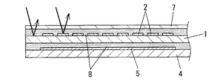
図1は本発明の第1の実施の形態によるタッチパネルの断面図、図2は同分解斜視図であり、同図において、1はポリエチレンテレフタレートやポリエーテルサルホン、ポリカーボネート等のフィルム状で光透過性の上基板で、上面には酸化珪素や酸化チタン、酸化ジルコニウム等の無機酸化物の、光透過性で単層または複数層に形成された反射変換層12が設けられている。
FIG. 1 is a cross-sectional view of a touch panel according to a first embodiment of the present invention, FIG. 2 is an exploded perspective view thereof, and 1 is a light transmission in the form of a film of polyethylene terephthalate, polyethersulfone, polycarbonate or the like. The upper surface is provided with a
そして、この反射変換層12上面には、酸化インジウム錫や酸化錫等の光透過性で略帯状の複数の上導電層2が、スパッタ法等によって前後方向に配列形成されると共に、一端が上導電層2端部に連結され他端が上基板1の外周右端に延出する、酸化インジウム錫等の上に蒸着等によって銅や銀等が重ねられた複数の上電極3が、上導電層2とは直交方向の左右方向に延出形成されている。
On the upper surface of the
さらに、上基板1上面には、アクリルやゴム等にキノフタロン系やアゾ系、キノン系、キサンテン系、フタロシアニン系、トリフェニルメタン系、ポリメチン系、アズレニウム系、スクアリウム系、金属錯体等の所定の色素顔料を分散した反射低減接着層13が、印刷や塗布等によって形成されている。
Further, on the upper surface of the
また、4は上基板1と同様のフィルム状で光透過性の下基板で、上面には反射変換層12と同様の反射変換層15が設けられると共に、この反射変換層15上面には、酸化インジウム錫や酸化錫等の光透過性で略帯状の複数の下導電層5が、上導電層2とは直交方向の左右方向に配列形成されている。
そして、一端が下導電層5端部に連結され他端が下基板4の外周右端に延出する上電極3と同様の複数の下電極6が、下導電層5と平行方向の左右方向に延出形成されると共に、下基板4上面には反射低減接着層13と同様の、反射低減接着層16が形成されている。
A plurality of
なお、複数の上導電層2と下導電層5は、複数の方形部が帯状に連結されて形成されると共に、これらの間には、略方形の複数の空隙部が設けられ、上基板1と下基板4が積重された状態では、各々の方形部が各々の空隙部に上下で交互に重なるように形成されている。
The plurality of upper
さらに、7はフィルム状で光透過性のカバー基板で、下基板4上面に上基板1、上基板1上面にカバー基板7が重ねられると共に、これらが反射低減接着層13や16によって貼り合わされて、タッチパネルが構成されている。
Further,
そして、このように構成されたタッチパネルが、液晶表示素子等の表示素子の前面に配置されて電子機器に装着されると共に、外周右端に延出した複数の上電極3や下電極6が、フレキシブル配線板やコネクタ(図示せず)等を介して、機器の電子回路(図示せず)に電気的に接続される。
The touch panel configured as described above is disposed on the front surface of a display element such as a liquid crystal display element and attached to an electronic device, and a plurality of upper electrodes 3 and
以上の構成において、電子回路から複数の上電極3と下電極6へ順次電圧が印加された状態で、タッチパネル背面の表示素子の表示に応じて、カバー基板7上面を指等で触れて操作すると、この操作した箇所の上導電層2と下導電層5の間の静電容量が変化するため、これによって操作された箇所を電子回路が検出し、機器の様々な機能の切換えが行われる。
In the above configuration, when a voltage is sequentially applied from the electronic circuit to the plurality of upper electrodes 3 and the
つまり、例えば複数のメニュー等が背面の表示素子に表示された状態で、所望のメニュー上のカバー基板7上面に指等を触れると、この指に電荷の一部が導電して、操作した箇所のタッチパネルの上導電層2と下導電層5の間の容量が変化し、これを電子回路が検出することによって、所望のメニューの選択等が行われるように構成されている。
That is, for example, when a finger or the like is touched on the upper surface of the
そして、この時、上基板1や下基板4上面に形成された反射変換層12や15、反射低減接着層13や16によって、上方から入射した太陽光や電灯等の外部光の反射が低減されると共に、略帯状の複数の上導電層2や下導電層5の輪郭が見えることを防ぎ、タッチパネル背面の表示素子の表示が見易く、容易で確実な操作が行えるようになっている。
At this time, the
すなわち、先ず、上基板1や下基板4上面に設けられた、所定の色素顔料を分散した反射低減接着層13や16によって、これらに分散された所定の色素顔料が、上方から入射した太陽光や電灯等の外部光の所定色の光を吸収して、上基板1や下基板4上面、上導電層2や下導電層5上面での外部光の反射を低減できるように構成されている。
That is, first, by the reflection reducing
また、上基板1や下基板4上面に設けられた単層または複数層の、反射変換層12や15の屈折率を1.4〜2に形成し、上導電層2や下導電層5の屈折率を2前後に近似したものとすることによって、図1に示すように、例えば反射変換層12上面と、上導電層2上面での反射光の差を少なくし、略帯状の複数の上導電層2や下導電層5の輪郭が見えることを防ぐようになっている。
Further, the refractive index of the single layer or multiple layers of the
ただ、このような酸化インジウム錫等の上導電層2や下導電層5、無機酸化物の反射変換層12や15は、一般に厚さが数十〜数百nm前後の薄膜状に形成されているため、上記のように反射光の差は少なくできるが、反射光が所定の色調、例えば赤色等を帯びた反射光になり易く、これによってタッチパネル背面の視認性が阻害されてしまう場合がある。
However, the upper
しかし、本発明においては、上基板1や下基板4上面には反射低減接着層13や16が設けられているため、この所定の色調を帯びた反射光も、反射低減接着層13や16内に分散された所定の色素顔料によって吸収され、上記のような所定の色調の反射光による、タッチパネル背面の表示素子の表示の見えづらさを防止できるようになっている。
However, in the present invention, since the reflection reducing
また、反射低減接着層13や16内に分散する色素顔料としては、上述したように様々なものがあるが、上方から入射する外部光や、上導電層2や下導電層5上面、反射変換層12や15上面での反射に合わせ、所定の光の波長に応じて、これらの選定を行うことができる。
In addition, as described above, there are various pigments dispersed in the reflection reducing
つまり、波長が400nm付近の青色光を吸収する場合には、キノフタロン系やアゾ系、キノン系、金属錯体等の黄色の色素顔料、波長が630〜640nm付近の黄色光を吸収する場合には、キサンテン系やフタロシアニン系、トリフェニルメタン系、アゾ系、キノン系、ポリメチン系、金属錯体等の青色の色素顔料、波長が710〜750nm付近の赤色光を吸収する場合には、フタロシアニン系やアズレニウム系、トリフェニルメタン系、キノン系、ポリメチン系、スクアリウム系、金属錯体等の緑色の色素顔料を分散することで、外部光の反射を低減し、タッチパネル背面の表示素子の表示を見易いものとすることが可能となる。 That is, when absorbing blue light having a wavelength of around 400 nm, yellow pigments such as quinophthalone, azo, quinone, and metal complexes, and absorbing yellow light having a wavelength of around 630 to 640 nm, Blue pigments such as xanthene, phthalocyanine, triphenylmethane, azo, quinone, polymethine, metal complexes, etc. When absorbing red light with a wavelength of around 710 to 750 nm, phthalocyanine or azulenium Disperse green pigments such as triphenylmethane, quinone, polymethine, squalium, metal complexes, etc., to reduce reflection of external light and make the display on the back of the touch panel easy to see Is possible.
なお、反射低減接着層13や16によって、上記の波長が400nm付近、630〜640nm付近、710〜750nm付近では透過率が5〜20%前後低下するが、波長が380〜780nmの可視光全体としては、85〜90%前後の透過率を得ることができるようになっている。
Incidentally, the reflection reducing
また、以上の説明では、上基板1と下基板4の両方の上面に反射低減接着層13と16を形成した構成について説明したが、いずれか一方、例えば上基板1の上面のみに反射低減接着層13を設けた構成としても、本発明の実施は可能である。
In the above description, the configuration in which the reflection reducing
このように本実施の形態によれば、上基板1や下基板4の上面に設けられた接着層を、所定の色素顔料を分散した反射低減接着層13や16で形成することによって、反射低減接着層13や16が所定色の光を吸収し、上方から入射した太陽光や電灯等の外部光の反射を低減できるため、タッチパネル背面の表示素子の表示が見易く、容易で確実な操作が可能なタッチパネルを得ることができるものである。
As described above, according to the present embodiment, the adhesive layer provided on the upper surface of the
(実施の形態2)
実施の形態2を用いて、本発明の特に請求項2記載の発明について説明する。
(Embodiment 2)
A second embodiment of the present invention, particularly the invention according to
なお、実施の形態1の構成と同一構成の部分には同一符号を付して、詳細な説明を省略する。
In addition, the same code | symbol is attached | subjected to the part of the structure same as the structure of
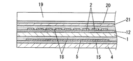
図3は本発明の第2の実施の形態によるタッチパネルの断面図であり、同図において、上基板1上面に無機酸化物の反射変換層12が形成されると共に、この反射変換層12上面に酸化インジウム錫等の光透過性で略帯状の複数の上導電層2や、酸化インジウム錫等の上に銅や銀等が重ねられた複数の上電極3(図示せず)が延出形成されていることは、実施の形態1の場合と同様である。
FIG. 3 is a cross-sectional view of a touch panel according to a second embodiment of the present invention. In FIG. 3, an inorganic oxide
そして、下基板4上面には同じく反射変換層15が形成され、この上面に下導電層5が上導電層2とは直交方向に配列形成されていることや、上電極3と同様の複数の下電極6(図示せず)が延出形成されていることも、実施の形態1の場合と同様であるが、上基板1や下基板4上面には、アクリルやゴム等の接着層18が設けられている。
Similarly, a
また、19はガラスやアクリル等の板状、またはポリカーボネート等のフィルム状で光透過性の透光板で、この上面には、アクリルやゴム等にキノフタロン系やアゾ系、キノン系、キサンテン系、フタロシアニン系、トリフェニルメタン系、ポリメチン系、アズレニウム系、スクアリウム系、金属錯体等の所定の色素顔料を分散した反射低減接着層20が、印刷や塗布等によって形成されている。
Further, 19 is a light-transmitting light-transmitting plate in the form of a plate such as glass or acrylic, or a film such as polycarbonate. On this upper surface, quinophthalone, azo, quinone, xanthene, A reflection-reducing
さらに、21はポリエチレンテレフタレートやポリカーボネート等のフィルム状で光透過性のカバーシートで、下基板4上面に上基板1、上基板1上面に透光板19、透光板19上面にカバーシート21が重ねられると共に、これらが接着層18や反射低減接着層20によって貼り合わされて、タッチパネルが構成されている。
Furthermore, 21 is a film-like light-transmitting cover sheet such as polyethylene terephthalate or polycarbonate. The
なお、このように構成されたタッチパネルが、液晶表示素子等の表示素子の前面に配置されて電子機器に装着され、複数の上電極3や下電極6が、機器の電子回路(図示せず)に電気的に接続されることは、実施の形態1の場合と同様である。
In addition, the touch panel comprised in this way is arrange | positioned in the front surface of display elements, such as a liquid crystal display element, and is mounted | worn with an electronic device, and the several upper electrode 3 and the
また、以上の構成において、タッチパネル背面の表示素子に複数のメニュー等が表示された状態で、所望のメニュー上のカバーシート21上面を指等で触れて操作すると、この指に電荷の一部が導電して、操作した箇所のタッチパネルの上導電層2と下導電層5の間の容量が変化し、これを電子回路が検出して、所望のメニューの選択等の機器の様々な機能の切換えが行われることも、実施の形態1の場合と同様である。
In the above configuration, when a plurality of menus and the like are displayed on the display element on the back surface of the touch panel, when the upper surface of the
さらに、この時、上基板1や下基板4上面に設けられた単層または複数層の、反射変換層12や15によって、図3に示すように、例えば反射変換層12上面と、上導電層2上面での反射光の差を少なくし、略帯状の複数の上導電層2や下導電層5の輪郭が見えることを防ぐように形成されていることも、実施の形態1の場合と同様であるが、同時に、透光板19上面に形成された反射低減接着層20によって、外部光や反射変換層12や15の所定の色調を帯びた反射光を低減できるようになっている。
Further, at this time, the single layer or plural layers of the reflective conversion layers 12 and 15 provided on the upper surfaces of the
つまり、本実施の形態においては、透光板19上面に設けられた所定の色素顔料を分散した反射低減接着層20によって、上方から入射した太陽光や電灯等の外部光の所定色の光を、反射低減接着層20に分散された所定の色素顔料が吸収して、上導電層2や下導電層5上面等での外部光の反射を低減すると共に、反射変換層12や15からの所定の色調を帯びた反射光も反射低減接着層20が吸収することで、タッチパネル背面の表示素子の表示が見易く、容易で確実な操作が行えるように構成されている。
In other words, in the present embodiment, the reflection-reducing
なお、以上の説明では、透光板19上面に反射低減接着層20を形成した構成について説明したが、図4の断面図に示すように、透光板19下面に反射低減接着層20を設け、カバーシート21を介して上基板1に貼付した構成としても、本発明の実施は可能である。
In the above description, the configuration in which the reflection reducing
また、以上の説明では、複数の上電極3や下電極6を、酸化インジウム錫等の上にスパッタ法や蒸着等によって、銅や銀等を重ねて形成した構成として説明したが、銀やカーボン等を印刷して、上電極3や下電極6を形成した構成としてもよい。
In the above description, the plurality of upper electrodes 3 and
このように本実施の形態によれば、上基板1の上面に配設された透光板19の上面または下面に設けられた接着層を、所定の色素顔料を分散した反射低減接着層20で形成することによって、反射低減接着層20が所定色の光を吸収し、上方から入射した太陽光や電灯等の外部光の反射を低減できるため、タッチパネル背面の表示素子の表示が見易く、容易で確実な操作が可能なタッチパネルを得ることができるものである。
As described above, according to the present embodiment, the adhesive layer provided on the upper surface or the lower surface of the
本発明によるタッチパネルは、良好な視認性が得られ、確実な操作が可能なものを得ることができるという有利な効果を有し、主に各種電子機器の操作用として有用である。 The touch panel according to the present invention has an advantageous effect that good visibility can be obtained and a reliable operation can be obtained, and is mainly useful for operation of various electronic devices.
1 上基板
2 上導電層
3 上電極
4 下基板
5 下導電層
6 下電極
7 カバー基板
12、15 反射変換層
13、16、20 反射低減接着層
18 接着層
19 透光板
21 カバーシート
DESCRIPTION OF
Claims (2)
Priority Applications (3)
| Application Number | Priority Date | Filing Date | Title |
|---|---|---|---|
| JP2011144034A JP2013012020A (en) | 2011-06-29 | 2011-06-29 | Touch panel |
| US13/524,470 US9033524B2 (en) | 2011-06-29 | 2012-06-15 | Touch panel |
| CN2012102253119A CN102866799A (en) | 2011-06-29 | 2012-06-29 | Touch panel |
Applications Claiming Priority (1)
| Application Number | Priority Date | Filing Date | Title |
|---|---|---|---|
| JP2011144034A JP2013012020A (en) | 2011-06-29 | 2011-06-29 | Touch panel |
Publications (2)
| Publication Number | Publication Date |
|---|---|
| JP2013012020A true JP2013012020A (en) | 2013-01-17 |
| JP2013012020A5 JP2013012020A5 (en) | 2014-08-07 |
Family
ID=47390422
Family Applications (1)
| Application Number | Title | Priority Date | Filing Date |
|---|---|---|---|
| JP2011144034A Pending JP2013012020A (en) | 2011-06-29 | 2011-06-29 | Touch panel |
Country Status (3)
| Country | Link |
|---|---|
| US (1) | US9033524B2 (en) |
| JP (1) | JP2013012020A (en) |
| CN (1) | CN102866799A (en) |
Cited By (1)
| Publication number | Priority date | Publication date | Assignee | Title |
|---|---|---|---|---|
| JP2016515743A (en) * | 2013-04-20 | 2016-05-30 | ティーピーケイ タッチ ソリューションズ(シアメン)インコーポレーテッド | Touch panel and manufacturing method thereof |
Families Citing this family (2)
| Publication number | Priority date | Publication date | Assignee | Title |
|---|---|---|---|---|
| KR101976637B1 (en) * | 2012-10-11 | 2019-05-10 | 엘지이노텍 주식회사 | Touch panel and method for manufacturing the same |
| CN107533395A (en) * | 2015-07-31 | 2018-01-02 | 惠普发展公司有限责任合伙企业 | Touch-screen light absorbing layer |
Citations (7)
| Publication number | Priority date | Publication date | Assignee | Title |
|---|---|---|---|---|
| JP2000305715A (en) * | 1999-04-23 | 2000-11-02 | Sharp Corp | Resistance film type touch panel and liquid crystal display device with resistance film type touch panel |
| JP2002268569A (en) * | 2001-03-14 | 2002-09-20 | Mitsui Chemicals Inc | Optical filter |
| JP2002307594A (en) * | 2001-04-17 | 2002-10-23 | Nof Corp | Transmissive hue correction material and use thereof |
| JP2010020682A (en) * | 2008-07-14 | 2010-01-28 | Brother Ind Ltd | Color correction sheet and display device using the color correction sheet |
| JP2010027052A (en) * | 2008-07-18 | 2010-02-04 | Samsung Corning Precision Glass Co Ltd | Contact input detecting display filter and display equipped with the same |
| JP2010027391A (en) * | 2008-07-18 | 2010-02-04 | Nitto Denko Corp | Transparent conductive film and touch panel |
| JP2010208169A (en) * | 2009-03-11 | 2010-09-24 | Gunze Ltd | Transparent planar article and transparent touch switch |
Family Cites Families (5)
| Publication number | Priority date | Publication date | Assignee | Title |
|---|---|---|---|---|
| JP5116004B2 (en) | 2006-08-03 | 2013-01-09 | 日東電工株式会社 | Transparent conductive laminate and touch panel provided with the same |
| JP4667471B2 (en) * | 2007-01-18 | 2011-04-13 | 日東電工株式会社 | Transparent conductive film, method for producing the same, and touch panel provided with the same |
| JP2009093397A (en) | 2007-10-09 | 2009-04-30 | Panasonic Corp | Touch panel and input device using the same |
| CN101452351B (en) | 2007-12-03 | 2010-11-17 | 义强科技股份有限公司 | High luminous transmittance touch control device |
| CN101498972B (en) | 2008-02-01 | 2012-07-18 | 台达电子工业股份有限公司 | Touching control panel |
-
2011
- 2011-06-29 JP JP2011144034A patent/JP2013012020A/en active Pending
-
2012
- 2012-06-15 US US13/524,470 patent/US9033524B2/en active Active
- 2012-06-29 CN CN2012102253119A patent/CN102866799A/en active Pending
Patent Citations (7)
| Publication number | Priority date | Publication date | Assignee | Title |
|---|---|---|---|---|
| JP2000305715A (en) * | 1999-04-23 | 2000-11-02 | Sharp Corp | Resistance film type touch panel and liquid crystal display device with resistance film type touch panel |
| JP2002268569A (en) * | 2001-03-14 | 2002-09-20 | Mitsui Chemicals Inc | Optical filter |
| JP2002307594A (en) * | 2001-04-17 | 2002-10-23 | Nof Corp | Transmissive hue correction material and use thereof |
| JP2010020682A (en) * | 2008-07-14 | 2010-01-28 | Brother Ind Ltd | Color correction sheet and display device using the color correction sheet |
| JP2010027052A (en) * | 2008-07-18 | 2010-02-04 | Samsung Corning Precision Glass Co Ltd | Contact input detecting display filter and display equipped with the same |
| JP2010027391A (en) * | 2008-07-18 | 2010-02-04 | Nitto Denko Corp | Transparent conductive film and touch panel |
| JP2010208169A (en) * | 2009-03-11 | 2010-09-24 | Gunze Ltd | Transparent planar article and transparent touch switch |
Cited By (2)
| Publication number | Priority date | Publication date | Assignee | Title |
|---|---|---|---|---|
| JP2016515743A (en) * | 2013-04-20 | 2016-05-30 | ティーピーケイ タッチ ソリューションズ(シアメン)インコーポレーテッド | Touch panel and manufacturing method thereof |
| KR101763783B1 (en) | 2013-04-20 | 2017-08-01 | 티피케이 터치 솔루션즈 (씨아먼) 인코포레이티드 | Touch control panel and manufacturing method therefor |
Also Published As
| Publication number | Publication date |
|---|---|
| US9033524B2 (en) | 2015-05-19 |
| US20130003182A1 (en) | 2013-01-03 |
| CN102866799A (en) | 2013-01-09 |
Similar Documents
| Publication | Publication Date | Title |
|---|---|---|
| US9429988B2 (en) | Touch screen panel | |
| US9188802B2 (en) | Display device integrated with touch screen | |
| JP6324656B2 (en) | Touch panel substrate and display device | |
| US8643629B2 (en) | Color filter with touch screen function and liquid crystal display device | |
| US9419612B2 (en) | Touch panel | |
| CN103150049A (en) | Touch screen panel with frame free of chromatic aberration and manufacturing method thereof | |
| US10496232B2 (en) | Capacitive touch panel | |
| US20120292170A1 (en) | Touch panel | |
| JP6707836B2 (en) | Sensor electrode base material for touch panel integrated organic electroluminescence display device, touch panel integrated organic electroluminescence display device, and method for manufacturing touch panel integrated organic electroluminescence display device | |
| JP2013161203A (en) | Touch panel sensor substrate and display unit equipped with the same | |
| JP2013008272A (en) | Decorative transparent protection substrate integrated touch panel and manufacturing method thereof | |
| TWI401498B (en) | Flat display touch panel and fabricating method of the same | |
| JP2012068287A (en) | Color filter substrate and method of manufacturing the same | |
| JP2013214173A (en) | Capacitance-type film sensor, and sensor module and cover module using the same | |
| JP6361106B2 (en) | Substrate with transparent conductive film, touch panel substrate, touch panel integrated front protective plate for display device, and display device | |
| JP5869007B2 (en) | Capacitive touch panel substrate and display device | |
| US9207815B2 (en) | Input device and method of manufacturing the same | |
| JP2014179063A (en) | Touch panel | |
| JP2013077305A (en) | Display device and electronic apparatus | |
| JP2013012020A (en) | Touch panel | |
| KR102281616B1 (en) | Touch screen panel and method of manufacturing the same | |
| TWI472984B (en) | Touch panel and touch-controlled display device | |
| US11061504B2 (en) | Input sensing unit and display device including the same | |
| JP2013206198A (en) | Touch sensor | |
| JP2013171128A (en) | Wired front face protective plate for display device, method for manufacturing the same, and display device |
Legal Events
| Date | Code | Title | Description |
|---|---|---|---|
| A521 | Request for written amendment filed |
Free format text: JAPANESE INTERMEDIATE CODE: A523 Effective date: 20140625 |
|
| A621 | Written request for application examination |
Free format text: JAPANESE INTERMEDIATE CODE: A621 Effective date: 20140625 |
|
| RD01 | Notification of change of attorney |
Free format text: JAPANESE INTERMEDIATE CODE: A7421 Effective date: 20140714 |
|
| A711 | Notification of change in applicant |
Free format text: JAPANESE INTERMEDIATE CODE: A711 Effective date: 20141007 |
|
| A977 | Report on retrieval |
Free format text: JAPANESE INTERMEDIATE CODE: A971007 Effective date: 20150330 |
|
| A131 | Notification of reasons for refusal |
Free format text: JAPANESE INTERMEDIATE CODE: A131 Effective date: 20150331 |
|
| A02 | Decision of refusal |
Free format text: JAPANESE INTERMEDIATE CODE: A02 Effective date: 20150728 |